US11218029B2 - Detecting apparatus, power receiving apparatus, power transmitting apparatus, and contactless power supply system - Google Patents
Detecting apparatus, power receiving apparatus, power transmitting apparatus, and contactless power supply system Download PDFInfo
- Publication number
- US11218029B2 US11218029B2 US16/019,708 US201816019708A US11218029B2 US 11218029 B2 US11218029 B2 US 11218029B2 US 201816019708 A US201816019708 A US 201816019708A US 11218029 B2 US11218029 B2 US 11218029B2
- Authority
- US
- United States
- Prior art keywords
- coil
- detector
- coils
- receiver
- power supply
- Prior art date
- Legal status (The legal status is an assumption and is not a legal conclusion. Google has not performed a legal analysis and makes no representation as to the accuracy of the status listed.)
- Expired - Fee Related, expires
Links
Images


Classifications
-
- H—ELECTRICITY
- H02—GENERATION; CONVERSION OR DISTRIBUTION OF ELECTRIC POWER
- H02J—ELECTRIC POWER NETWORKS; CIRCUIT ARRANGEMENTS OR SYSTEMS FOR SUPPLYING OR DISTRIBUTING ELECTRIC POWER; SYSTEMS FOR STORING ELECTRIC ENERGY
- H02J50/00—Circuit arrangements or systems for wireless supply or distribution of electric power
- H02J50/60—Circuit arrangements or systems for wireless supply or distribution of electric power responsive to the presence of foreign objects, e.g. detection of living beings
-
- H—ELECTRICITY
- H02—GENERATION; CONVERSION OR DISTRIBUTION OF ELECTRIC POWER
- H02J—ELECTRIC POWER NETWORKS; CIRCUIT ARRANGEMENTS OR SYSTEMS FOR SUPPLYING OR DISTRIBUTING ELECTRIC POWER; SYSTEMS FOR STORING ELECTRIC ENERGY
- H02J50/00—Circuit arrangements or systems for wireless supply or distribution of electric power
- H02J50/10—Circuit arrangements or systems for wireless supply or distribution of electric power using inductive coupling
- H02J50/12—Circuit arrangements or systems for wireless supply or distribution of electric power using inductive coupling of the resonant type
-
- G—PHYSICS
- G01—MEASURING; TESTING
- G01N—INVESTIGATING OR ANALYSING MATERIALS BY DETERMINING THEIR CHEMICAL OR PHYSICAL PROPERTIES
- G01N27/00—Investigating or analysing materials by the use of electric, electrochemical, or magnetic means
-
- G—PHYSICS
- G01—MEASURING; TESTING
- G01N—INVESTIGATING OR ANALYSING MATERIALS BY DETERMINING THEIR CHEMICAL OR PHYSICAL PROPERTIES
- G01N27/00—Investigating or analysing materials by the use of electric, electrochemical, or magnetic means
- G01N27/72—Investigating or analysing materials by the use of electric, electrochemical, or magnetic means by investigating magnetic variables
-
- G—PHYSICS
- G01—MEASURING; TESTING
- G01V—GEOPHYSICS; GRAVITATIONAL MEASUREMENTS; DETECTING MASSES OR OBJECTS; TAGS
- G01V3/00—Electric or magnetic prospecting or detecting; Measuring magnetic field characteristics of the earth, e.g. declination, deviation
- G01V3/08—Electric or magnetic prospecting or detecting; Measuring magnetic field characteristics of the earth, e.g. declination, deviation operating with magnetic or electric fields produced or modified by objects or geological structures or by detecting devices
- G01V3/10—Electric or magnetic prospecting or detecting; Measuring magnetic field characteristics of the earth, e.g. declination, deviation operating with magnetic or electric fields produced or modified by objects or geological structures or by detecting devices using induction coils
- G01V3/101—Electric or magnetic prospecting or detecting; Measuring magnetic field characteristics of the earth, e.g. declination, deviation operating with magnetic or electric fields produced or modified by objects or geological structures or by detecting devices using induction coils by measuring the impedance of the search coil; by measuring features of a resonant circuit comprising the search coil
-
- G—PHYSICS
- G01—MEASURING; TESTING
- G01V—GEOPHYSICS; GRAVITATIONAL MEASUREMENTS; DETECTING MASSES OR OBJECTS; TAGS
- G01V3/00—Electric or magnetic prospecting or detecting; Measuring magnetic field characteristics of the earth, e.g. declination, deviation
- G01V3/08—Electric or magnetic prospecting or detecting; Measuring magnetic field characteristics of the earth, e.g. declination, deviation operating with magnetic or electric fields produced or modified by objects or geological structures or by detecting devices
- G01V3/10—Electric or magnetic prospecting or detecting; Measuring magnetic field characteristics of the earth, e.g. declination, deviation operating with magnetic or electric fields produced or modified by objects or geological structures or by detecting devices using induction coils
- G01V3/104—Electric or magnetic prospecting or detecting; Measuring magnetic field characteristics of the earth, e.g. declination, deviation operating with magnetic or electric fields produced or modified by objects or geological structures or by detecting devices using induction coils using several coupled or uncoupled coils
- G01V3/105—Electric or magnetic prospecting or detecting; Measuring magnetic field characteristics of the earth, e.g. declination, deviation operating with magnetic or electric fields produced or modified by objects or geological structures or by detecting devices using induction coils using several coupled or uncoupled coils forming directly coupled primary and secondary coils or loops
-
- H—ELECTRICITY
- H02—GENERATION; CONVERSION OR DISTRIBUTION OF ELECTRIC POWER
- H02J—ELECTRIC POWER NETWORKS; CIRCUIT ARRANGEMENTS OR SYSTEMS FOR SUPPLYING OR DISTRIBUTING ELECTRIC POWER; SYSTEMS FOR STORING ELECTRIC ENERGY
- H02J50/00—Circuit arrangements or systems for wireless supply or distribution of electric power
- H02J50/40—Circuit arrangements or systems for wireless supply or distribution of electric power using two or more transmitting or receiving devices
-
- H—ELECTRICITY
- H02—GENERATION; CONVERSION OR DISTRIBUTION OF ELECTRIC POWER
- H02J—ELECTRIC POWER NETWORKS; CIRCUIT ARRANGEMENTS OR SYSTEMS FOR SUPPLYING OR DISTRIBUTING ELECTRIC POWER; SYSTEMS FOR STORING ELECTRIC ENERGY
- H02J50/00—Circuit arrangements or systems for wireless supply or distribution of electric power
- H02J50/70—Circuit arrangements or systems for wireless supply or distribution of electric power involving the reduction of electric, magnetic or electromagnetic leakage fields
-
- H—ELECTRICITY
- H02—GENERATION; CONVERSION OR DISTRIBUTION OF ELECTRIC POWER
- H02J—ELECTRIC POWER NETWORKS; CIRCUIT ARRANGEMENTS OR SYSTEMS FOR SUPPLYING OR DISTRIBUTING ELECTRIC POWER; SYSTEMS FOR STORING ELECTRIC ENERGY
- H02J50/00—Circuit arrangements or systems for wireless supply or distribution of electric power
- H02J50/80—Circuit arrangements or systems for wireless supply or distribution of electric power involving the exchange of data, concerning supply or distribution of electric power, between transmitting devices and receiving devices
-
- H02J7/025—
-
- H—ELECTRICITY
- H02—GENERATION; CONVERSION OR DISTRIBUTION OF ELECTRIC POWER
- H02J—ELECTRIC POWER NETWORKS; CIRCUIT ARRANGEMENTS OR SYSTEMS FOR SUPPLYING OR DISTRIBUTING ELECTRIC POWER; SYSTEMS FOR STORING ELECTRIC ENERGY
- H02J7/00—Circuit arrangements for charging or discharging batteries or for supplying loads from batteries
- H02J7/40—Circuit arrangements for charging or discharging batteries or for supplying loads from batteries characterised by the exchange of charge or discharge related data
- H02J7/42—Circuit arrangements for charging or discharging batteries or for supplying loads from batteries characterised by the exchange of charge or discharge related data with electronic devices having internal batteries, e.g. mobile phones
-
- H04B5/0037—
-
- H04B5/0087—
-
- H—ELECTRICITY
- H04—ELECTRIC COMMUNICATION TECHNIQUE
- H04B—TRANSMISSION
- H04B5/00—Near-field transmission systems, e.g. inductive or capacitive transmission systems
- H04B5/20—Near-field transmission systems, e.g. inductive or capacitive transmission systems characterised by the transmission technique; characterised by the transmission medium
- H04B5/24—Inductive coupling
- H04B5/26—Inductive coupling using coils
- H04B5/263—Multiple coils at either side
-
- H—ELECTRICITY
- H04—ELECTRIC COMMUNICATION TECHNIQUE
- H04B—TRANSMISSION
- H04B5/00—Near-field transmission systems, e.g. inductive or capacitive transmission systems
- H04B5/70—Near-field transmission systems, e.g. inductive or capacitive transmission systems specially adapted for specific purposes
- H04B5/79—Near-field transmission systems, e.g. inductive or capacitive transmission systems specially adapted for specific purposes for data transfer in combination with power transfer
Definitions
- the present disclosure relates to a magnetic coupling element that magnetically couples with another magnetic coupling element or foreign matter, and to an apparatus (magnetic coupling apparatus) and system (magnetic coupling system) utilizing such a magnetic coupling element.
- the present disclosure relates to a detecting apparatus, a power receiving apparatus, a power transmitting apparatus, and a contactless power supply system configured to detect the presence of foreign matter (such as metal, a magnetized body, or magnet) which may generate heat due to magnetic flux between a contactless power supplying apparatus and an electronic device constituting a contactless power supply system.
- foreign matter such as metal, a magnetized body, or magnet
- CE consumer electronics
- a CE device such as a mobile phone or portable music player
- a contactless manner referred to as contactless power supply systems or contactless power transfer systems, for example.
- charging is initiated not by inserting (connecting) the connector of an AC adapter or other power supply apparatus into a CE device, but rather by simply placing an electronic device (the secondary device) onto a charging tray (the primary device). In other words, a terminal connection between the electronic device and the charging tray is unnecessary.
- Electromagnetic induction is established as a technique for supplying power in a contactless manner as above. Meanwhile, contactless power supply systems using a technique called magnetic resonance which utilizes the resonance phenomenon have been gaining attention recently.
- Contactless power supply systems using magnetic resonance are advantageous in that the principle of the resonance phenomenon may be utilized to transfer power between devices separated by greater distances than those of electromagnetic induction. Additionally, there is an advantage in that the transfer efficiency (power supply efficiency) does not fall significantly even if the axis alignment between the power source (transmitter coil) and power recipient (receiver coil) is somewhat poor.
- magnetic resonance-based systems and electromagnetic induction-based systems are alike in that both are contactless power supply systems (magnetic coupling systems) utilizing a power source (transmitter coil; a magnetic coupling element) and a power recipient (receiver coil; a magnetic coupling element).
- one important element in contactless power supply systems is the thermal regulation of foreign matter, such as metals, magnetized bodies, and magnets, which may generate heat due to magnetic flux. If foreign matter becomes interposed in the gap between the transmitter coil and the receiver coil when supplying power in a contactless manner, there is a risk of causing the foreign matter to generate heat due to the magnetic flux passing through that foreign matter. This risk is not limited to electromagnetic induction-based or magnetic resonance-based systems. Such heat generation in foreign matter may lead to currents being produced in a foreign metal due to the magnetic flux passing through the foreign metal (eddy currents, current loops, circular currents), or to hysteresis loss being produced in a foreign magnetized body or foreign magnet due to the magnetic flux passing through the foreign magnetized body or foreign magnet.
- JP 2008-206231A proposes a method of detecting foreign metal according to the modulation rate (information on amplitude and phase changes) during communication between the transmitter and receiver
- JP 2001-275280A proposes a method of detecting foreign metal according to eddy current loss (foreign matter detection according to DC-DC efficiency).
- JP 2008-206231A and JP 2001-275280A do not take into account the effects of a metal housing at the receiver.
- some kind of metal such as a metal housing or metal components
- JP 2001-275280A it is indeterminate whether eddy current loss occurs because of the metal housing of the portable device, or because foreign metal is present between the transmitter and receiver. In this way, it can hardly be said that the techniques proposed in JP 2008-206231A and JP 2001-275280A are able to accurately detect foreign metal.
- an embodiment according to the embodiment of the present disclosure detects foreign matter in close proximity to a detector coil (in other words, a magnetic coupling element) without providing an additional sensor, and furthermore improves detection accuracy.
- a detecting apparatus including one or a plurality of magnetic coupling elements that include a plurality of coils, and a detector that measures an electrical parameter related to the one or plurality of magnetic coupling elements or to a circuit that at least includes the one or plurality of magnetic coupling elements, and determines from a change in the electrical parameter whether a foreign matter that generates heat due to magnetic flux is present.
- the plurality of coils are electrically connected such that magnetic flux produced from at least one or more of the plurality of coils and magnetic flux produced from remaining coils of the plurality of coils have approximately opposing orientations.
- FIG. 1 is a schematic circuit diagram accompanying an explanation of Q factor measurement used as an example of foreign metal detection according to an embodiment of the present disclosure
- FIG. 2 is a diagrammatic exterior illustration of a contactless power supply system according to the first embodiment of the present disclosure
- FIG. 3 is a block diagram illustrating an exemplary configuration of a contactless power supply system according to the first embodiment of the present disclosure
- FIGS. 4A, 4B and 4C are circuit diagrams illustrating exemplary configurations of a resonant circuit
- FIG. 5 is a schematic diagram of an exemplary diagrammatic configuration of a transmitter coil and a receiver coil in a contactless power supply system according to the first embodiment of the present disclosure
- FIGS. 6A and 6B are explanatory diagrams illustrating an exemplary detailed configuration of a detector coil and receiver coil according to the first embodiment of the present disclosure, where FIG. 6A is an exemplary perspective view configuration and FIG. 6B is an exemplary plan view configuration of the detector coil and receiver coil in the case where the difference between the inner dimension of the detector coil and the inner dimension of the receiver coil is ⁇ 4 mm;
- FIGS. 7A and 7B are plan views illustrating an exemplary detailed configuration of a detector coil and receiver coil according to the first embodiment of the present disclosure, where FIG. 7A illustrates an exemplary plan view configuration of the detector coil and receiver coil in the case where the difference between the inner dimension of the detector coil and the inner dimension of the receiver coil is 0 mm, and FIG. 7B is an exemplary plan view configuration of the detector coil and receiver coil in the case where the difference between the inner dimension of the detector coil and the inner dimension of the receiver coil is +4 mm;
- FIGS. 8A and 8B are plan views illustrating an exemplary detailed configuration of a detector coil and receiver coil according to a first comparative example, where FIG. 8A illustrates an exemplary detailed configuration of the detector coil and receiver coil in the case where the difference between the inner dimension of the detector coil and the inner dimension of the receiver coil is ⁇ 4 mm, and FIG. 8B is an exemplary detailed configuration of the detector coil and receiver coil in the case where the difference between the inner dimension of the detector coil and the inner dimension of the receiver coil is 0 mm;
- FIG. 9 is a graph of examples illustrating to what degree the detector coil Q factor changes depending on the presence or absence of a receiver coil in the case of modifying the inner dimension of the detector coil;
- FIG. 10A is a diagrammatic cross-section view regarding a spiral-shaped coil and the distribution of magnetic field lines produced from that coil
- FIG. 10B is a diagrammatic cross-section view regarding a figure 8-shaped coil according to an embodiment of the present disclosure and the distribution of magnetic field lines from that coil;
- FIG. 11A is a waveform diagram illustrating an example of a waveform of voltage (voltage waveform) produced in an LC resonator (resonant circuit) including a detector coil and a resonant capacitor C 3 in the case where a spiral-shaped detector coil is disposed inside the receiver coil illustrated in FIG. 8A
- FIG. 11B is a waveform diagram illustrating an example of a waveform of voltage (voltage waveform) produced in an LC resonator including a detector coil and a resonant capacitor C 3 in the case where a figure 8-shaped detector coil is disposed inside the receiver coil illustrated in FIG. 6B ;
- FIG. 12 is a graph illustrating an example of the difference in the power supply efficiency of a contactless power supply system according to whether or not a foreign matter detecting apparatus is present;
- FIG. 13A is a performance mapping illustrating exemplary foreign metal detection accuracy for the case of using a figure 8-shaped coil as a detector coil
- FIG. 13B is a performance mapping illustrating exemplary foreign metal detection accuracy for the case of using a spiral-shaped coil as a detector coil
- FIG. 14 is a plan view illustrating an exemplary configuration of a figure 8-shaped detector coil according to a first modification of the first embodiment of the present disclosure
- FIG. 15 is a plan view illustrating an exemplary configuration of a square grid-shaped detector coil according to the second embodiment of the present disclosure
- FIG. 16 is a plan view illustrating an exemplary configuration of a square grid-shaped detector coil according to a first modification of the second embodiment of the present disclosure
- FIG. 17 is a plan view illustrating an exemplary configuration of a lattice-shaped detector coil according to the third embodiment of the present disclosure.
- FIG. 18 is a plan view illustrating an example of a detector coil unit in which two figure 8-shaped detector coils are disposed according to the fourth embodiment of the present disclosure
- FIG. 19 is a plan view illustrating an example of a detector coil unit in which two figure 8-shaped detector coils are disposed according to a first modification of the fourth embodiment of the present disclosure
- FIGS. 20A, 20B and 20C are explanatory diagrams for exemplary detector coil arrangements according to the fifth embodiment of the present disclosure, where FIGS. 20A, 20B, and 20C are plan views illustrating an example of a receiver coil, an example in which multiple detector coils are disposed on top of the receiver coil, and an example in which some detector coils are disposed in the center of the receiver coil, respectively;
- FIGS. 21A, 21B and 21C are explanatory diagrams for exemplary detector coil arrangements according to the sixth embodiment of the present disclosure, where FIGS. 21A, 21B, and 21C are plan views illustrating an example of a receiver coil and foreign metal, an example in which multiple detector coils are disposed on top of the receiver coil, and an example in which multiple detector coils are additionally disposed on top of the multiple detector coils in FIG. 21B , respectively; and
- FIGS. 22A and 22B are explanatory diagrams for exemplary detector coil arrangements according to a first modification of the sixth embodiment of the present disclosure, where FIGS. 22A and 22B are plan views illustrating an example in which multiple detector coils are disposed on top of the receiver coil, and an example in which multiple detector coils are additionally disposed on top of the multiple detector coils in FIG. 22A , respectively.
- a magnetic coupling system that detects foreign matter on the basis of an electrical parameter for a circuit at a transmitter or a receiver when charging a component such as a battery in the receiver (secondary device) with power supplied from the transmitter (primary device).
- an electrical parameter is measured for a circuit in a transmitter or a receiver, the circuit at least including one or multiple magnetic coupling elements which magnetically couple with an external element and which are realized with multiple coils. The presence of foreign matter in close proximity to the magnetic coupling element is then determined on the basis of the electrical parameter measurement results.
- the above circuit at least including a magnetic coupling element is a resonant circuit
- the above electrical parameter is the quality factor (Q factor).
- the Q factor is an index expressing the relationship between energy storage and loss, and is typically used as a factor expressing the sharpness of the resonance peak (in other words, the resonance strength) in a resonant circuit.
- FIG. 1 is a schematic circuit diagram accompanying an explanation of Q factor measurement used for foreign metal detection according to an embodiment of the present disclosure.
- the circuit illustrated in FIG. 1 is an example of a basic circuit layout (for the case of magnetic coupling) illustrating the principle of Q factor measurement.
- the circuit is provided with a signal source 1 , which includes an alternating current (AC) power source 2 that produces an AC signal (sine wave) and a resistive element 3 , as well as a capacitor 4 and a coil 5 .
- the resistive element 3 is an illustration of the internal resistance (output impedance) of the AC power source 2 .
- the capacitor 4 and the coil 5 are connected to the signal source 1 so as to form a series resonant circuit (one example of a resonant circuit).
- the resonant circuit resonates at a given frequency (the resonant frequency) according to the capacitance value (C value) of the capacitor 4 and the inductance value (L value) of the coil 5 .
- FIG. 1 illustrates a circuit provided with a series resonant circuit realized with a coil 5 and a capacitor 4 , various layouts are conceivable for the detailed configuration, insofar as resonant circuit functionality is provided.
- the magnetic field lines will pass through the metal fragment, and eddy currents will be produced in the metal fragment.
- the metal fragment and the coil 5 are magnetically coupled and it appears as though a resistive load has been attached to the coil 5 , changing the Q factor of the coil (resonant circuit). Measuring the Q factor thus leads to detection of foreign metal near the coil 5 (in other words, a magnetically coupled state).
- V 1 the voltage across the ends of the coil 5 and the capacitor 4 constituting the series resonant circuit (an example of voltage applied to a resonant circuit)
- V 2 the voltage across the ends of the coil 5
- the Q factor of the series resonant circuit is expressed as in Eq. 1, where R is the effective resistance value (series resistance value) for the frequency f of the circuit, L is the inductance value, and C is the capacitance value.
- the voltage V 2 is obtained by multiplying the voltage V 1 by a factor of approximately Q. It is established that the series resistance value R and the inductance value L indicated in Eq. 1 change as metal approaches or due to the effects of eddy currents produced in the metal. For example, if a metal fragment approaches the coil 5 , the effective resistance value R increases, and the Q factor drops. In other words, since the Q factor of the resonant circuit and the resonant frequency change greatly due to the effects of metal present in the vicinity of the coil 5 , by detecting such change it is possible to detect a metal fragment present near the coil 5 . Additionally, such Q factor measurement may be applied to the detection of foreign metal interposed between a transmitter (primary device) and a receiver (secondary device).
- detector coil that electromagnetically or magnetically couples with an external element to measure the Q factor of the circuit using an AC signal at a different frequency than the frequency of the AC signal flowing through the transmitter coil and the receiver coil.
- AC signals for contactless power supply are separable from AC signals for Q factor measurement, and thus it becomes possible to measure the Q factor while contactless power supply is in operation.
- accurate detection of foreign metal or other matter may be conducted even while contactless power supply is in operation.
- the detector coil may be greatly affected by the magnetic flux (lines of magnetic force; a magnetic field) for contactless power supply in the case of using a typical spiral-shaped coil 5 as the detector coil that electromagnetically or magnetically couples with an external element.
- AC signals for Q factor measurement utilized in foreign matter detection may overlap AC signals for contactless power supply, producing unwanted noise due to the contactless power supply.
- foreign metal detection accuracy may decrease greatly.
- the above detector coil is readily affected by the transmitter coil and receiver coil used for contactless power supply, as well as by elements such as magnetic materials and metal inside the electronic device housing.
- the Q factor of the detector coil which is used as the basis value for determining the presence of foreign metal, may decrease greatly.
- foreign metal detection accuracy may change greatly depending on the configuration of the power source (transmitter) and power recipient (receiver) in the contactless power supply system.
- the inventors propose a magnetic coupling element that improves foreign matter detection accuracy by obtaining more exact information for foreign matter detection, as well as a foreign matter detecting apparatus using such a magnetic coupling element.
- FIG. 2 illustrates an exemplary diagrammatic configuration of a contactless power supply system given as a magnetic coupling system according to the first embodiment of the present disclosure
- FIG. 3 illustrates an exemplary block configuration of a contactless power supply system according to the first embodiment of the present disclosure.
- the contactless power supply system 100 illustrated in FIG. 2 is a system that transfers (supplies) power in a contactless manner using a magnetic field (in the present embodiment, using magnetic resonance).
- the contactless power supply system 100 is equipped with a power supply apparatus 10 (the primary device) and one or multiple electronic devices (secondary devices) given as power recipient devices.
- a power supply apparatus 10 the primary device
- secondary devices the electronic devices
- an electronic device 20 A in the form of a mobile phone handset and an electronic device 20 B in the form of a digital still camera are provided as power recipient devices, for example.
- a power recipient device is not limited to this example, and may be any electronic device able to receive power from the power supply apparatus 10 in a contactless manner.
- the contactless power supply system 100 is configured such that power is transferred from the power supply apparatus 10 to the electronic devices 20 A and 20 B by placing the electronic devices 20 A and 20 B onto or in proximity to a power supply surface (transmitter surface) S 1 of the power supply apparatus 10 .
- the power supply apparatus 10 has a mat shape (or tray shape) with the surface area of the power supply surface S 1 being greater than devices such as the power recipient electronic devices 20 A and 20 B, in consideration of the case of transferring power to multiple electronic devices 20 A and 20 B simultaneously or in a time division (successively).
- the power supply apparatus 10 is an apparatus (such as a charging tray) that transfers power to electronic devices 20 A and 20 B using a magnetic field. As illustrated in FIG. 3 , for example, the power supply apparatus 10 is equipped with a power transmitting apparatus 11 that transfers power using power supplied from a power source 9 external to the power supply apparatus 10 .
- the external power source 9 may be, for example, an electric utility from which power is supplied via a plug socket, otherwise called a power outlet.
- the power transmitting apparatus 11 includes a transmitter 12 , a high-frequency power generator circuit 13 , a detector circuit 14 , an impedance matching circuit 15 , a controller circuit 16 , and a resonant capacitor (capacitive element) C 1 , for example.
- the power transmitting apparatus 11 in this example takes a block configuration enabling the contactless power supply system 100 to conduct unidirectional communication using load modulation.
- the configuration is not limited thereto in cases where unidirectional communication using a technique other than load modulation or bidirectional communication is considered.
- the transmitter 12 includes components such as a transmitter coil (primary coil) L 1 discussed later ( FIG. 5 ).
- the transmitter 12 uses the transmitter coil L 1 and the resonant capacitor C 1 to transfer power to the electronic devices 20 A and 20 B (specifically, to a receiver 22 discussed later) using a magnetic field.
- the transmitter 12 includes functionality for emitting a magnetic field (magnetic flux) from the power supply surface S 1 towards the electronic devices 20 A and 20 B. A detailed configuration of the transmitter 12 will be discussed later.
- the high-frequency power generator circuit 13 is a circuit that uses power supplied from the power source 9 external to the power supply apparatus 10 to generate given high-frequency power (an AC signal) for the purpose of power transfer, for example.
- the detector circuit 14 is a circuit that includes functionality for detecting (demodulating) a modulated signal from a load modulator circuit 29 discussed later.
- the detector circuit 14 supplies detection results to the controller circuit 16 .
- the impedance matching circuit 15 is a circuit that matches impedance during power transfer. In so doing, efficiency during power transfer (the transfer efficiency) is improved. Note that, depending on the configuration of components such as the transmitter coil L 1 and a receiver coil L 2 discussed later, or the resonant capacitors C 1 and C 2 , it may also be configured such that the impedance matching circuit 15 is not provided. Also, if decreased transfer efficiency is not a concern, it may be configured such that the impedance matching circuit 15 is not provided.
- the resonant capacitor C 1 is a capacitive element constituting part of the transmitter coil L 1 of the transmitter 12 as well as the LC resonator (resonant circuit), and is disposed with respect to the transmitter coil L 1 so as to form an electrical series connection, parallel connection, or a combined series and parallel connection.
- a resonant frequency (first resonant frequency) f 1 whose frequency is approximately equal or near that of the high-frequency power generated in the high-frequency power generator circuit 13 .
- the capacitance value of the resonant capacitor C 1 is also set so as to obtain such a resonant frequency f 1 .
- the resonant capacitor C 1 is not provided if the above resonant frequency f 1 is realized by resonant operation using a potential difference across the windings in the transmitter coil L 1 or a parasitic capacitance component (stray capacitance component) realized by a potential difference between the transmitter coil L 1 and the receiver coil L 2 discussed later. Also, if decreased transfer efficiency is not a concern, it may be similarly configured such that the resonant capacitor C 1 is not provided.
- the controller circuit 16 is a circuit that receives detection results from the detector circuit 14 and controls components such as the high-frequency power generator circuit 13 , the impedance matching circuit 15 , the resonant capacitor C 1 , and the transmitter 12 .
- the controller circuit 16 in the power transmitting apparatus 11 is able to confirm the presence of foreign metal, making it possible to restrict or stop power transfer under control by the controller circuit 16 .
- the controller circuit 16 also receives detection results from the detector circuit 14 and applies pulse-width modulation control (PWM control) to the high-frequency power generator circuit 13 and switching control to the impedance matching circuit 15 , the resonant capacitor C 1 , and the transmitter 12 .
- PWM control pulse-width modulation control
- Such control by the controller circuit 16 also enables automatic control for maintaining a high transfer efficiency (power supply efficiency).
- Electronic devices such as stationary electronic devices typified by televisions or portable electronic devices typified by mobile phones and digital cameras, including rechargeable batteries, are applicable as the electronic devices 20 A and 20 B.
- the electronic device 20 A and the electronic device 20 B are provided with similar functionality with respect to power supply, and in the description hereinafter, the electronic device 20 A will be described as a representative example.
- the electronic device 20 A is equipped with a power receiving apparatus 21 and a load 27 that performs given action (action that elicits functionality as an electronic device) on the basis of power supplied from the power receiving apparatus 21 .
- the electronic device 20 A is also equipped with a foreign matter detecting apparatus 31 for detecting the presence of foreign metal between (in the gap between) the transmitter 12 and the receiver 22 .
- the power receiving apparatus 21 includes a receiver 22 , a resonant capacitor (capacitive element) C 2 , an impedance matching circuit 23 , a rectifier circuit 24 , a voltage stabilizer circuit 25 , a controller circuit 26 , a battery 28 , and a load modulator circuit 29 .
- the power receiving apparatus 21 in this example takes a block configuration enabling the contactless power supply system 100 to conduct unidirectional communication using load modulation.
- the configuration is not limited thereto in cases where unidirectional communication using a technique other than load modulation or bidirectional communication is considered.
- the receiver 22 includes components such as a receiver coil (secondary coil) L 2 discussed later ( FIG. 5 ).
- the receiver 22 includes functionality for using the receiver coil L 2 and the resonant capacitor C 2 to receive power transferred from the transmitter 12 in the power supply apparatus 10 .
- a detailed configuration of the receiver 22 will be discussed later.
- the resonant capacitor C 2 is a capacitive element constituting part of the receiver coil L 2 of the receiver 22 as well as the LC resonator (resonant circuit), and is disposed with respect to the receiver coil L 2 so as to form an electrical series connection, parallel connection, or a combined series and parallel connection.
- a resonant frequency (second resonant frequency) f 2 whose frequency is approximately equal or near that of the high-frequency power generated in the high-frequency power generator circuit 13 of the power transmitting apparatus 11 .
- the LC resonator including the transmitter coil L 1 and the resonant capacitor C 1 in the power transmitting apparatus 11 and the LC resonator including the receiver coil L 2 and the resonant capacitor C 2 in the power receiving apparatus 21 resonate with each other at approximately equal resonant frequencies (f 1 ⁇ f 2 ).
- the capacitance value of the resonant capacitor C 2 is also set so as to obtain such a resonant frequency f 2 .
- the resonant capacitor C 2 is also not provided if the above resonant frequency f 1 is realized by resonant operation using a potential difference across the windings in the receiver coil L 2 or a parasitic capacitance component realized by a potential difference between the transmitter coil L 1 and the receiver coil L 2 . Also, if decreased transfer efficiency is not a concern, it may also be configured such that the resonant frequency f 2 and the resonant frequency f 1 differ from each other (f 2 ⁇ f 1 ), and the resonant capacitor C 2 is not provided.
- the impedance matching circuit 23 is a circuit that matches impedance during power transfer, similarly to the impedance matching circuit 15 in the above power transmitting apparatus 11 . Note that, depending on the configuration of components such as the transmitter coil L 1 and the receiver coil L 2 discussed later, or the resonant capacitors C 1 and C 2 , it may also be configured such that the impedance matching circuit 23 is also not provided. Also, if decreased transfer efficiency is not a concern, it may be similarly configured such that the impedance matching circuit 23 is also not provided.
- the rectifier circuit 24 is a circuit that rectifies the power (AC power) supplied from the receiver 22 to generate direct current (DC) power. Note that a smoothing circuit (not illustrated) for smoothing rectified power is often provided between the rectifier circuit 24 and the voltage stabilizer circuit 25 discussed later.
- the voltage stabilizer circuit 25 is a circuit that conducts given voltage stabilization on the basis of DC power supplied from the rectifier circuit 24 , and charges the battery 28 or a battery (not illustrated) in the load 27 .
- the battery 28 stores power in response to being charged by the voltage stabilizer circuit 25 , and may be realized using a rechargeable battery (secondary cell) such as a lithium-ion battery, for example. Note that the battery 28 may also be omitted in cases where only the battery in the load 27 is used, for example.
- a rechargeable battery secondary cell
- the battery 28 may also be omitted in cases where only the battery in the load 27 is used, for example.
- the load modulator circuit 29 is a circuit for applying load modulation, and changes in the power state due to load modulation may be detected with the detector circuit 14 in the power transmitting apparatus 11 . In other words, if given the load modulator circuit 29 and the controller circuit 26 discussed later, it becomes possible to transmit information in the power receiving apparatus 21 to the power transmitting apparatus 11 without providing a special communication apparatus in the electronic device 20 A.
- the controller circuit 26 is a circuit for controlling charging operation with respect to the battery 28 or the battery (not illustrated) in the load 27 .
- the controller circuit 26 is also a circuit for controlling load modulation in the load modulator circuit 29 , and applies control enabling the power transmitting apparatus 11 to recognize that foreign metal has been detected by having changes in the power state due to such load modulation be detected with the detector circuit 14 in the power transmitting apparatus 11 .
- the controller circuit 26 may apply charging control to restrict or stop power transfer to the power receiving apparatus 21 in the electronic device 20 A.
- the foreign matter detecting apparatus 31 includes a detector coil L 3 , a resonant capacitor C 3 , a foreign matter detector circuit 32 , and a controller circuit 33 .
- the foreign matter detector circuit 32 and the controller circuit 33 may constitute a detector.
- the detector coil L 3 is an example of a magnetic coupling element for detecting foreign metal, and is provided separately from the transmitter coil L 1 and the receiver coil L 2 . Further details will be discussed later ( FIGS. 4A, 4B, 4C, 6A, 6B, 7A, 7B, 14-19, and 20A, 20B, 20C, 21A, 21B, 21C, 22A and 22B ).
- the resonant capacitor C 3 is a capacitor connected to the detector coil L 3 in an electrical series configuration (see FIG. 4A ), or a capacitor connected to the detector coil L 3 in a combined electrical series and parallel configuration (resonant capacitors C 3 - 1 and C 3 - 2 ) (see FIGS. 4B and 4C ). By connecting the resonant capacitor C 3 , the detector coil L 3 resonates at a given frequency f 3 (LC resonance).
- the resonant capacitor C 3 may be connected to the detector coil L 3 in an electrical parallel configuration (not illustrated).
- the foreign matter detector circuit 32 is a circuit for measuring the Q factor of the detector coil L 3 or the Q factor of the LC resonator including the detector coil L 3 and the resonant capacitor C 3 by using an AC signal whose frequency (f 3 , where f 3 ⁇ f 2 and f 3 ⁇ f 2 ) differs from the frequencies (f 1 and f 2 , where f 1 ⁇ f 2 ) of the AC signals flowing through the transmitter coil L 1 and the receiver coil L 2 .
- the Q factor of the detector coil L 3 or the Q factor of the LC resonator including the detector coil L 3 and the resonant capacitor C 3 may be computed by measuring voltage values at the two locations (the voltage value V 1 and the voltage value V 2 ) illustrated in FIGS. 4A, 4B, and 4C as described earlier with the foreign matter detector circuit 32 , and then taking their ratio (V 2 /V 1 ), for example.
- the frequency characteristics related to properties such as the impedance and admittance are able to be measured with the foreign matter detector circuit 32 , it is also possible to compute the Q factor of the detector coil L 3 or the LC resonator from the ratio of the peak frequency at which the frequency characteristics reach a peak versus the frequency width where that peak value is halved (WHM) (thus, peak frequency/WHM).
- the Q factor from the ratio of the real part versus the imaginary part of the impedance of the resonant circuit.
- the real part and the imaginary part of the impedance may be computed using an auto-balancing bridge circuit and a vector ratio detector, for example.
- the controller circuit 33 is a circuit that controls the foreign matter detector circuit 32 , while also determining the presence of foreign metal between (in the gap between) the transmitter 12 and the receiver 22 from the measurement results by the foreign matter detector circuit 32 .
- the controller circuit 33 is also a circuit for transmitting the determination result to the controller circuit 26 of the power receiving apparatus 21 .
- the controller circuit 33 may, for example, compare a measured Q factor to a threshold value saved in memory (not illustrated) in advance, and determine that foreign metal is present near the detector coil in the case where the measured Q factor is less than the threshold value.
- FIG. 5 is a schematic illustration of an exemplary diagrammatic configuration of the transmitter 12 and the receiver 22 in a contactless power supply system according to the first embodiment of the present disclosure.
- the transmitter 12 includes at least one (in this case, one) transmitter coil L 1
- the receiver 22 includes at least one (in this case, one) receiver coil L 2 . It is possible for the transmitter coil L 1 and the receiver coil L 2 to be magnetically coupled to each other. Note that it may also be configured such that the transmitter 12 and the receiver 22 includes one or multiple coils or one or multiple LC resonators including coils and capacitors in addition to the transmitter coil L 1 and the receiver coil L 2 .
- These coils are not limited to being open coils (conductive coils) shaped like conductive wire (material) wound multiple times, but may also be open loops (conductive loops) shaped like conductive wire wound one time.
- the coil or loop used as such a conductive coil or conductive loop may be a coil (wound coil) or loop (wound loop) in which conductive wire is wound, or a coil (patterned coil) or loop (patterned loop) formed by a conductive pattern on a printed substrate (printed circuit board) or flexible printed substrate (flexible printed circuit board), for example. Also, it is possible to form such a patterned coil and patterned loop by printing or depositing conductive material, or by machining a conductive metal plate or sheet, for example.
- FIG. 5 simultaneously illustrates an exemplary distribution of magnetic field lines produced from the transmitter coil L 1 at a given phase.
- the transmitter coil L 1 is a coil for transferring power using magnetic flux (lines of magnetic force; a magnetic field).
- the transmitter coil L 1 is a coil for producing magnetic flux (lines of magnetic force; a magnetic field).
- the receiver coil L 2 is a coil for receiving power from the magnetic flux (lines of magnetic force; a magnetic field) transferred from the transmitter 12 .
- FIGS. 6A and 6B are illustrations of an exemplary detailed configuration of the detector coil L 3 and the receiver coil L 2 according to the first embodiment of the present disclosure, where FIG. 6A is an exemplary perspective view configuration and FIG. 6B is an exemplary plan view configuration (exemplary X-Y plan view configuration).
- the receiver coil L 2 illustrated in FIGS. 6A and 6B are spiral-shaped coils.
- the transmitter coil L 1 and the receiver coil L 2 are spiral-shaped coils, helical coils, or coils with a combined spiral and helical shape, for example.
- the transmitter coil L 1 and the receiver coil L 2 are not limited thereto.
- the detector coil L 3 illustrated in FIGS. 6A and 6B are figure 8-shaped coils realized by a combination of a spiral-shaped coil L 31 and a spiral-shaped coil L 32 that distributes magnetic flux of approximately the opposite orientation of the orientation of the magnetic flux from the coil L 31 .
- the detector coil L 3 is simply a spiral-shaped coil, helical coil, or a coil with a combined spiral and helical shape, foreign metal detection accuracy may greatly decrease.
- the detector coil L 3 is desirable for the detector coil L 3 to be a coil able to distribute magnetic flux (magnetic field lines; a magnetic field) over a surface with approximately opposing orientations, such as a figure 8-shaped, square grid-shaped, or lattice-shaped coil as discussed later.
- a detector coil with such a shape yields advantages such as enabling decreased magnetic flux leakage from the detector coil, decreased change in the electrical properties (such as the Q factor and L value) of the detector coil due to external factors, and a decrease in unwanted noise occurring in the detector coil. For this reason, it is possible to greatly improve foreign metal detection accuracy.
- the coil or loop used as the detector coil L 3 may be a coil (wound coil) or loop (wound loop) in which conductive wire is wound, or a coil (patterned coil) or loop (patterned loop) formed by a conductive pattern on a printed substrate (printed circuit board) or flexible printed substrate (flexible printed circuit board), for example. Also, it is possible to form such a patterned coil and patterned loop by printing or depositing conductive material, or by machining a conductive metal plate or sheet, for example.
- the receiver coil L 2 and the detector coil L 3 may be disposed in the same plane, the receiver coil L 2 and the detector coil L 3 may also be disposed in different planes. However, for the sake of the packaging area with respect to the electronic device 20 A ( 20 B), in many cases it is desirable to form the receiver 22 (receiver coil L 2 ) and the detector coil L 3 in the same plane. In the example in FIGS. 6A and 6B , the receiver coils L 2 and the detector coil L 3 are not disposed in the same plane for the sake of comparison as illustrated in FIG. 9 , discussed later.
- the inner dimension (the dimension of the innermost perimeter) of the detector coils L 3 is smaller than the inner dimension C (the dimension of the innermost perimeter) of the receiver coil L 2
- the outer dimension B (the dimension of the outermost perimeter) of the detector coil L 3 is smaller than the inner dimension C (the dimension of the innermost perimeter) of the receiver coil L 2 .
- FIGS. 6A and 6B compared the inner dimension A and the outer dimension B along the shorter edge of the figure 8-shaped detector coil L 3 to the inner dimension C along the shorter edge of the receiver coil L 2
- the dimensions may also be compared using the respective inner dimensions and outer dimensions along the longer edge (such as the inner dimension A′ along the longer edge of the detector coil L 3 , for example). It is further desirable if the inner dimension and outer dimension along both the shorter edge and the longer edge of the detector coil are smaller than the inner dimensions along both the shorter edge and the longer edge of the receiver coil.
- the configuration is not limited thereto in applications where foreign metal detection accuracy is not demanded.
- the detector coil L 3 is electrically insulated from (i.e., not connected to an electrical contact point or other element in) the transmitter 12 (transmitter coil L 1 ) and the receiver 22 (receiver coil L 2 ), the configuration is not limited thereto.
- magnetic shielding material 41 is disposed between the housing 40 of the electronic device, and the receiver coil L 2 and detector coil L 3 .
- the magnetic shielding material 41 is provided for the purpose of decreasing magnetic flux leakage from the receiver coil L 2 and raising the Q factors of the receiver coil L 2 and the detector coil L 3 , but may also be omitted as appropriate.
- the magnetic shielding material 41 herein may be realized with magnetic material such as ferrite, conductive metal such as metal, or a combination of magnetic material and conductive metal, for example.
- FIGS. 7A and 7B illustrate different examples of the difference between the inner dimension of the detector coil L 3 and the inner dimension of the receiver coil L 2 in the exemplary detailed configuration of the detector coil L 3 and the receiver coil L 2 in FIGS. 6A and 6B .
- FIG. 7A illustrates an exemplary detailed configuration of the detector coil L 3 and the receiver coil L 2 in the case where the difference between the inner dimension A of the detector coil L 3 and the inner dimension C of the receiver coil L 2 is 0 mm.
- FIG. 7B illustrates an exemplary detailed configuration of the detector coil L 3 and the receiver coil L 2 in the case where the difference between the inner dimension A of the detector coil L 3 and the inner dimension C of the receiver coil L 2 is +4 mm.
- the high-frequency power generator circuit 13 supplies given high-frequency power (an AC signal) for transferring power to the transmitter coil L 1 and the resonant capacitor C 1 (LC resonator) in the transmitter 12 .
- a magnetic field is produced in the transmitter coil L 1 in the transmitter 12 .
- an electronic device 20 A given as a power recipient (charging target) is placed (or brought near) the top surface (power supply surface S 1 ) of the power supply apparatus 10 , the transmitter coil L 1 in the power supply apparatus 10 and the receiver coil L 2 in the electronic device 20 A come into proximity near the power supply surface S 1 .
- a receiver coil L 2 is placed near a transmitter coil L 1 producing a magnetic field (magnetic flux), electromotive force, induced by the magnetic flux produced from the transmitter coil L 1 , is produced in the receiver coil L 2 .
- the transmitter coil L 1 and the receiver coil L 2 are respectively linked by electromagnetic induction or magnetic resonance, and a magnetic field is produced.
- power (indicated as the contactless power supply P 1 in FIG. 3 ) is transferred from the transmitter coil L 1 (primary coil; power supply apparatus 10 ; transmitter 12 ) to the receiver coil L 2 (secondary coil; electronic device 20 A; receiver 22 ).
- resonant operation using the transmitter coil L 1 and the resonant capacitor C 1 is conducted in the power supply apparatus 10 (at a resonant frequency f 1 ), while resonant operation using the receiver coil L 2 and the resonant capacitor C 2 is conducted in the electronic device 20 A (at a resonant frequency f 2 , where f 2 ⁇ f 1 ).
- AC power received by the receiver coil L 2 in the electronic device 20 A is supplied to the rectifier circuit 24 and the voltage stabilizer circuit 25 , and the following charging operation is performed. Namely, after the AC power is converted into given DC power by the rectifier circuit 24 , voltage stabilization based on the DC power is performed by the voltage stabilizer circuit 25 , and the battery 28 or a battery (not illustrated) in the load 27 is charged. In so doing, charging operation based on power received by the receiver 22 is performed in the electronic device 20 A.
- a terminal connection to an AC adapter is unnecessary when charging the electronic device 20 A, and charging may be easily initiated (contactless power supply may be performed) by simply placing the electronic device 20 A onto (or in proximity to) the power supply surface S 1 of the power supply apparatus 10 . This leads to a reduced burden on the user.
- the Q factor of a detector coil L 3 or an LC resonator including the detector coil L 3 and a resonant capacitor C 3 is measured using an AC signal whose frequency (f 3 , where f 3 ⁇ f 2 and f 3 ⁇ f 2 ) differs from the frequencies (f 1 and f 2 ) of the AC signals flowing through the transmitter coil L 1 and the receiver coil L 2 .
- the foreign matter detecting apparatus 31 is also able to determine the presence of foreign metal between (in the gap between) the transmitter 12 and the receiver 22 from the magnitude of change in this Q factor.
- a determination result by the foreign matter detecting apparatus 31 which indicates the presence or absence of foreign metal is transmitted from the power receiving apparatus 21 in the electronic device 20 A to the power transmitting apparatus 11 in the power supply apparatus 10 by a communication technique such as load modulation.
- control for restricting or stopping power transfer is applied by the controller circuit 16 in the power transmitting apparatus 11 or the controller circuit 26 in the power receiving apparatus 21 , for example.
- control for restricting or stopping power transfer is applied by the controller circuit 16 in the power transmitting apparatus 11 or the controller circuit 26 in the power receiving apparatus 21 , for example.
- FIGS. 8A and 8B are plan views illustrating an exemplary detailed configuration of a detector coil and receiver coil according to comparative examples.
- FIG. 8A illustrates an exemplary detailed configuration (exemplary X-Y plan view configuration) of a detector coil L 4 according to a first comparative example and the receiver coil L 2 , in the case where the difference between the inner dimension of the detector coil L 4 and the inner dimension of the receiver coil L 2 is ⁇ 4 mm.
- FIG. 8B illustrates an exemplary detailed configuration (exemplary X-Y plan view configuration) of a detector coil L 4 according to a second comparative example and the receiver coil L 2 , in the case where the difference between the inner dimension of the detector coil L 4 and the inner dimension of the receiver coil L 2 is 0 mm.
- these detector coils L 4 are simple spiral-shaped coils.
- data related to the detector coil Q factor is acquired by applying electromagnetic field analysis to an analysis model of a detector coil and a receiver coil like those illustrated in FIGS. 8A and 8B (see FIG. 9 ).
- the graph in FIG. 9 illustrates to what degree the Q factor of the detector coil L 4 changes depending on the presence or absence of the receiver coil L 2 in the case of modifying the inner dimension of the detector coil L 4 .
- factors such as the conductive wire type, thickness, width, and the length of the gap between conductive wires constituting the detector coil L 4 are not modified.
- FIG. 8A is an exemplary detailed configuration of a detector coil and a receiver coil in the case where the difference between the inner dimension of the detector coil and the inner dimension of the receiver coil is ⁇ 4 mm in the graph in FIG. 9 .
- FIG. 8B is an exemplary detailed configuration of a detector coil and a receiver coil in the case where the difference between the inner dimension of the detector coil and the inner dimension of the receiver coil is 0 mm in FIG. 9 .
- FIG. 9 demonstrates that in the case of using a spiral-shaped detector coil L 4 , the Q factor of the detector coil L 4 changes greatly depending on whether or not the receiver coil L 2 is present. In other words, FIG. 9 demonstrates that the Q factor of the detector coil L 4 decreases greatly when the receiver coil L 2 is present. This indicates that in the case of using a spiral-shaped detector coil L 4 , there is significant magnetic flux leakage from the detector coil L 4 , and the electrical properties (such as the Q factor and L value) of the detector coil L 4 change greatly due to external factors (such as the metal material or magnetic material constituting the transmitter coil L 1 , the receiver coil L 2 , the magnetic shielding material 41 , the power supply apparatus 10 , and the electronic device 20 A ( 20 B)).
- external factors such as the metal material or magnetic material constituting the transmitter coil L 1 , the receiver coil L 2 , the magnetic shielding material 41 , the power supply apparatus 10 , and the electronic device 20 A ( 20 B)
- FIG. 9 demonstrates that foreign metal detection accuracy is greatly decreased in the case of using a spiral-shaped coil as the detector coil. Furthermore, FIG. 9 also demonstrates that as the inner dimension A of the detector coil L 4 becomes smaller with respect to the inner dimension C of the receiver coil L 2 (for example, if the difference between the detector coil inner dimension A and the receiver coil inner dimension C becomes less than or equal to 0 mm), the amount of decrease in the Q factor of the detector coil L 4 due to the presence of the receiver coil L 2 also becomes smaller (see the right side of FIG. 9 ).
- FIGS. 6A, 6B, 7A and 7B a figure 8-shaped detector coil L 3 is used, as illustrated in FIGS. 6A, 6B, 7A and 7B . All other parameters are basically the same as those of the first comparative example and the second comparative example.
- FIG. 9 illustrates to what degree the Q factor of the detector coil L 3 changes depending on the presence or absence of the receiver coil L 2 in the case of modifying the inner dimension of the detector coil L 3 .
- factors such as the conductive wire type, thickness, width, and the length of the gap between conductive wires constituting the detector coil L 3 are not modified.
- FIG. 9 demonstrates that in the case of using a figure 8-shaped detector coil L 3 , although the Q factor of the detector coil L 3 does change slightly depending on whether or not the receiver coil L 2 is present, the magnitude of that change is significantly smaller than in the case of using the spiral-shaped detector coil L 4 .
- FIG. 9 demonstrates that although the Q factor of the detector coil L 3 does change slightly due to the presence of the receiver coil L 2 , the magnitude of that change is significantly smaller than in the case of using the spiral-shaped detector coil L 4 .
- FIG. 9 demonstrates that in the case of using a figure 8-shaped coil as the detector coil, foreign metal detection accuracy is greatly improved compared to the case of using a spiral-shaped coil. Furthermore, FIG. 9 also demonstrates that as the inner dimension A of the detector coil L 3 becomes smaller with respect to the inner dimension C of the receiver coil L 2 (for example, if the difference between the detector coil inner dimension A and the receiver coil inner dimension C becomes less than or equal to 0 mm), the amount of decrease in the Q factor of the detector coil L 3 due to the presence of the receiver coil L 2 also becomes smaller.
- FIG. 9 demonstrates that the Q factor of the detector coil L 3 is greatest (maximized) in the case where the difference between the detector coil inner dimension A and the receiver coil inner dimension C is ⁇ 4 mm, and in the case where the difference between the detector coil inner dimension A and the receiver coil inner dimension C is 0 mm.
- FIG. 9 demonstrates that it is desirable for the inner dimension A of the detector coil L 3 to be smaller than the inner dimension C of the receiver coil L 2 .
- FIG. 9 demonstrates that it is desirable for the outer dimension B of the detector coil L 3 also to be smaller than the inner dimension C of the receiver coil L 2 .
- the configuration is not limited thereto in the case where it is desirable to extend the foreign metal detection range even if the foreign metal detection accuracy drops.
- FIG. 10A is a diagrammatic cross-section view regarding a spiral-shaped coil (the detector coil L 4 , for example) at a given time (phase) and the distribution of magnetic field lines produced from that coil.
- FIG. 10B is a diagrammatic cross-section view regarding a figure 8-shaped coil (the detector coil L 3 , for example) at a given time (phase) and the distribution of magnetic field lines from that coil.
- the distribution of magnetic field lines differs greatly between a spiral-shaped coil and a figure 8-shaped coil.
- the figure 8-shaped coil discussed above is configured to be able to distribute magnetic flux (magnetic field lines; a magnetic field) over a surface such that the magnetic flux from the two coils (the coils L 31 and L 32 , for example) constituting the figure 8-shaped coil have approximately opposing orientations.
- magnetic field lines are distributed so as to form a loop inside the coil.
- the magnetic field lines are less likely to be distributed farther compared to a spiral-shaped coil.
- the figure 8-shaped detector coil L 3 yields less magnetic flux leakage from the detector coil L 3 , and the electrical properties (such as the Q factor and L value) of the detector coil L 3 change less due to external factors (such as the metal material or magnetic material constituting the transmitter coil L 1 , the receiver coil L 2 , the magnetic shielding material 41 , the power supply apparatus 10 , and the electronic device 20 A ( 20 B)) compared to the spiral-shaped detector coil L 4 .
- FIG. 11A illustrates a waveform 45 a of voltage produced in an LC resonator including the detector coil L 4 and the resonant capacitor C 3 by causing actual contactless power supply operation using the power transmitting apparatus 11 and the power receiving apparatus 21 , in the case where the detector coil L 4 is provided inside the receiver coil L 2 as illustrated in FIG. 8A .
- voltage values (V 1 and V 2 ) are measured at two locations in an LC resonator including the detector coil L 4 and the resonant capacitor C 3 using an AC signal whose frequency (f 3 , where f 3 ⁇ f 2 and f 3 ⁇ f 2 ) differs from the frequencies (f 1 and f 2 , where f 1 ⁇ f 2 ) of the AC signals flowing through the transmitter coil L 1 and the receiver coil L 2 .
- the Q factor is then calculated from the ratio of these two voltage values.
- FIG. 11A demonstrates that in the case of using the spiral-shaped detector coil L 4 , an extremely large voltage unnecessary for foreign matter detection is produced due to the contactless power supply frequencies (f 1 and f 2 ).
- the voltage waveform 45 a has an effective value of 690 mV, and a peak-to-peak (p-p) value of 2.25 V.
- This voltage becomes a large source of unwanted noise when measuring voltage values at two locations in the LC resonator including the detector coil L 4 and the resonant capacitor C 3 .
- the foreign metal detection accuracy decreases greatly due to this unwanted noise.
- FIG. 11B illustrates a waveform 46 a of voltage produced in an LC resonator including the detector coil L 3 and the resonant capacitor C 3 by causing actual contactless power supply operation using the power transmitting apparatus 11 and the power receiving apparatus 21 , in the case where the detector coil L 3 is provided inside the receiver coil L 2 as illustrated in FIG. 6A .
- FIG. 11B demonstrates that, compared to the case of using the spiral-shaped detector coil L 4 , almost no voltage is produced due to the contactless power supply frequencies (f 1 and f 2 , where f 1 ⁇ f 2 ) in the case of using the figure 8-shaped detector coil L 3 .
- the voltage waveform 46 a has an effective value of 27.7 mV, and a peak-to-peak (p-p) value of 390 mV.
- FIG. 12 illustrates the difference in the power supply efficiency of a contactless power supply system 100 according to whether or not a foreign matter detecting apparatus 31 is present.
- the detector coil L 3 in the foreign matter detecting apparatus 31 is disposed inside the receiver coil L 2 in a relationship like that illustrated in FIGS. 6A and 6B .
- FIG. 12 demonstrates that there is almost no change in the power supply efficiency of a contactless power supply system 100 according to whether or not a foreign matter detecting apparatus 31 (the detector coil L 3 and the resonant capacitor C 3 ) is present.
- the detector coil L 3 has less magnetic flux leakage from the detector coil L 3 , and the electrical properties (such as the Q factor and L value) of the detector coil L 3 exhibit little change due to external factors (such as the metal material or magnetic material constituting the transmitter coil L 1 , the receiver coil L 2 , the magnetic shielding material 41 , the power supply apparatus 10 , and the electronic device 20 A ( 20 B)).
- FIGS. 13A and 13B illustrate the foreign metal detection accuracy of a detector coil.
- FIG. 13A is a performance mapping illustrating exemplary foreign metal detection accuracy for the case of using a figure 8-shaped coil as a detector coil. Note that in FIG. 13A , the Q factor of the detector coil is assumed to be 100% in the case of packaging the detector coil inside the electronic device 20 A.
- a figure 8-shaped detector coil is disposed on top of the transmitter 12 (transmitter coil L 1 ) of the power supply apparatus 10 , the detector coil is somewhat affected by the transmitter 12 (the transmitter coil L 1 , magnetic material, and internal metal, for example), and thus the Q factor of the detector coil drops somewhat (Q factor 47 b ) compared to when the power supply apparatus 10 is not present (Q factor 47 a ). However, since the drop in the Q factor of the detector coil is significantly greater in the case where foreign metal is disposed (Q factor 47 c ), foreign metal may be accurately detected.
- FIG. 13B is a performance mapping illustrating exemplary foreign metal detection accuracy for the case of using a spiral-shaped coil as a detector coil. Note that in FIG. 13B , the Q factor of the detector coil is assumed to be 100% in the case of packaging the detector coil inside the electronic device 20 A.
- a spiral-shaped detector coil is disposed on top of the transmitter 12 (transmitter coil L 1 ) of the power supply apparatus 10 , the detector coil is greatly affected by the transmitter 12 (the transmitter coil L 1 , magnetic material, and internal metal, for example), and thus the Q factor of the detector coil drops significantly (Q factor 48 b ) compared to when the power supply apparatus 10 is not present (Q factor 48 a ). For this reason, the Q factor of the detector coil does not change significantly even when foreign metal is disposed (Q factors 48 b and 48 c ), and thus the foreign metal detection accuracy worsens considerably in the case of using a spiral-shaped coil as the detector coil.
- applying a figure 8-shaped coil to the detector coil in a contactless power supply system equipped with a foreign matter detecting apparatus greatly improves factors such as magnetic flux leakage from the detector coil, change in the electrical properties (electrical parameters) due to external factors, and unwanted noise produced in the detector coil.
- factors such as magnetic flux leakage from the detector coil, change in the electrical properties (electrical parameters) due to external factors, and unwanted noise produced in the detector coil.
- the present embodiment is described using an example of detecting foreign matter while contactless power supply is in operation.
- an embodiment of the present disclosure is not limited only to such cases, and various modifications are possible.
- contactless power supply operation may be suspended or that power supplied by contactless power supply may be restricted while detecting foreign matter.
- the frequency of the AC signal flowing through the detector coil differ from the frequencies of the AC signals flowing through the transmitter coil and the receiver coil.
- foreign matter detection may be conducted using an AC signal whose frequency is approximately equal to the frequencies (f 1 ⁇ f 2 ) of the AC signals used for contactless power supply operation.
- the detector coil the same as the transmitter coil or the receiver coil.
- FIG. 14 Although the foregoing first embodiment is described only for the case of using a continuous figure 8-shaped detector coil as illustrated in FIGS. 6 and 7 , a figure 8-shaped detector coil (magnetic coupling element) like that illustrated in FIG. 14 may also be used.
- a figure 8-shaped detector coil L 3 ′ includes spiral-shaped coils L 31 and L 32 , with one end of the coil L 31 being electrically connected (joined) in series to one end of the coil L 32 using solder or a connector, for example.
- the coils L 31 and L 32 are connected such that the magnetic flux (magnetic field lines) produced from the coil L 31 and the magnetic flux (magnetic field lines) produced from the coil L 32 have approximately opposing orientations, as illustrated by FIG. 10B and the example in FIG. 14 .
- connection may also be an electrical parallel connection or a combined series and parallel connection.
- voltage may be measured using a lead 51 from the coil L 31 and a lead 52 from the coil L 32 .
- voltage may be measured between the junction 53 of the coil L 31 and the lead 51 or between the junction 53 of the coil L 32 and the coil L 32 , taking the junction 53 between the coil L 31 and the coil L 32 as a reference potential point.
- one or multiple magnetic coupling elements shaped like multiple coils electrically connected together in order to improve foreign matter detection accuracy, for example.
- one or multiple magnetic coupling elements shaped like multiple coils electrically connected together, in which the magnetic flux produced from at least one or more of these multiple coils and the magnetic flux produced from the remaining of these multiple coils have approximately opposing orientations.
- the configuration is not limited to a figure 8-shaped coil according to the first embodiment, and a square grid-shaped (in other words, a 2 ⁇ 2 lattice-shaped) coil may also be used as a detector coil (magnetic coupling element).
- a square grid-shaped coil in other words, a 2 ⁇ 2 lattice-shaped
- a detector coil magnetic coupling element
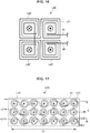
- FIG. 15 is a plan view illustrating an exemplary configuration of a square grid-shaped detector coil according to the second embodiment of the present disclosure.
- the square grid-shaped detector coil L 3 A includes four spiral-shaped coils L 31 to L 34 electrically connected (joined) in series.
- the coils L 33 and L 34 have a mostly similar configuration to the spiral-shaped coils L 31 and L 32 .
- the coil L 31 includes a lead 51
- the coil L 34 includes a lead 52 .
- the coil L 32 and the coil L 33 do not have leads, and are electrically connected to their respectively adjacent coils L 31 and L 34 .
- the coils L 31 to L 34 are connected such that the magnetic flux (magnetic field lines) produced from the coils L 31 and L 33 is of approximately opposite orientation to the magnetic flux (magnetic field lines) produced from the coils L 32 and L 34 at a given time (phase).
- connection may also be an electrical parallel connection or a combined series and parallel connection, similarly to the example in FIG. 14 .
- the relationship between the inner dimension A or the outer dimension B of the detector coil L 3 A and the receiver coil is likewise desirable for the relationship between the inner dimension A or the outer dimension B of the detector coil L 3 A and the receiver coil to be the relationship described in the first embodiment.
- a detector coil according to the second embodiment is a square grid-shaped coil including four coils. Increasing the number of coils compared to the figure 8-shaped coil according to the first embodiment increases the surface area occupied by the detector coil and increases the detection range. For example, in the case of a detector coil according to the second embodiment, the detection range may be doubled compared to a detector coil of the first embodiment.
- the decision to implement the first embodiment or the second embodiment may be determined according to whether detection accuracy or detection range is prioritized.
- FIG. 16 is a plan view illustrating an exemplary configuration of a square grid-shaped detector coil according to a first modification of the second embodiment of the present disclosure.
- the square grid-shaped detector coil L 3 B differs from the detector coil L 3 A in that the coils constituting the detector coil L 3 B are connected such that the magnetic flux (magnetic field lines) produced from the coils L 31 and L 34 ′ on which leads 51 and 52 are formed is of approximately opposite orientation to the magnetic flux (magnetic field lines) produced from the coils L 32 and L 33 ′ at a given time (phase).
- connection may also be an electrical parallel connection or a combined series and parallel connection, similarly to the example in FIG. 14 .
- the configuration is not limited to a square grid-shaped coil according to the above second embodiment, and a lattice-shaped coil may also be used as a detector coil (magnetic coupling element).
- a lattice-shaped coil may also be used as a detector coil (magnetic coupling element).
- an example applying a lattice-shaped coil to the detector coil will be described as a third embodiment of the present disclosure.
- FIG. 17 is a plan view illustrating an exemplary configuration of a lattice-shaped detector coil according to the third embodiment of the present disclosure.
- the lattice-shaped detector coil L 3 C is configured such that multiple coils are connected in an electrical series connection, parallel connection, or a combined series and parallel connection.
- the example in FIG. 17 is for the case of a detector coil that includes 21 spiral-shaped coils L 31 to L 321 connected in series.
- the coils L 31 to L 321 are disposed in a matrix parallel to the plane of the magnetic shielding material 41 , for example, with the coils from the coil L 31 to the coil L 321 being continuously connected in sequence.
- the coils L 31 to L 37 may be connected from left to right, with the coils L 38 to L 314 connected from right to left on the next row down, and the coils L 315 to L 321 connected from left to right one more row down.
- the coils L 31 to L 321 are connected such that the magnetic flux (magnetic field lines) produced from adjacent coils are of approximately opposing orientations at a given time (phase).
- a detector coil may be configured such that multiple coils such as spiral-shaped coils, helical coils, or coils with a combined spiral and helical shape (in other words, coils having a basic ring shape) are connected in an electrical series connection, parallel connection, or a combined series and parallel connection.
- these multiple coils constituting the detector coil it is desirable for these multiple coils constituting the detector coil to be connected such that the magnetic flux (magnetic field lines) produced from at least one or more of these multiple coils and the magnetic flux (magnetic field lines) produced from the remaining of these multiple coils have approximately opposing orientations at a given time (phase).
- the detector coil includes multiple coils
- the total magnetic flux (magnetic field lines) produced from at least one or more coils it is particularly desirable for the total magnetic flux (magnetic field lines) produced from at least one or more coils to be approximately equal to the total magnetic flux (magnetic field lines) of approximately opposite orientation produced from the remaining coils.
- issues such as magnetic flux leakage from the detector coil, changes in the electrical properties (electrical parameters) of the detector coil due to external factors, and unwanted noise occurring in the detector coil decrease particularly.
- the number of coils producing magnetic flux (magnetic field lines) of approximately opposite orientation is desirable for the number of coils producing magnetic flux (magnetic field lines) of approximately opposite orientation to be half the number of coils constituting the detector coil. In this case, since the magnetic flux distribution within the detector coil becomes approximately uniform, foreign metal detection accuracy stabilizes.
- At least one or more coils from among the multiple coils constituting the detector coil to have an inner dimension that is smaller than the inner dimension of the transmitter coil or the receiver coil.
- the overall inner dimension of the multiple coils constituting the detector coil may be smaller than the inner dimension of the transmitter coil or the receiver coil.
- the overall inner dimension of the multiple coils constituting the detector coil may be either the inner dimension A along the shorter edge or the inner dimension A′ along the longer edge, as illustrated in FIG. 17 .
- the overall outer dimension of the detector coil is smaller than the inner dimension of the transmitter coil or the receiver coil.
- the shape of the detector coil in order to effectively suppress unwanted noise produced in the detector coil, it is desirable for the shape of the detector coil to be an approximately symmetrical shape, such as by having approximate rotational symmetry, approximate line symmetry, or approximate point symmetry.
- the configuration is not limited thereto in the case where it is desirable to extend the foreign metal detection range even if the foreign metal detection accuracy drops.
- the number of coils constituting the detector coil is further increased compared to the second embodiment, and thus the detection range of the detector coil is significantly extended.
- an embodiment of the present disclosure is not limited to such a case, and may also be configured such that two or more detector coils (magnetic coupling elements) are multiply provided, as illustrated in FIGS. 18 and 19 , for example.
- the foreign matter detecting apparatus 31 may also be multiply provided.
- it may be configured such that one or multiple foreign matter detecting apparatus are able to switch among multiply disposed detector coils.
- FIG. 18 is a plan view of a detector coil unit 61 in which two figure 8-shaped detector coils are disposed according to the fourth embodiment of the present disclosure.
- detector coil unit 61 In the detector coil unit 61 in this example, two detector coils L 3 - 1 and L 3 - 2 are disposed adjacent to each other on the sides which are opposite the sides having their respective leads 51 and 52 .
- the detector coils L 3 - 1 and L 3 - 2 each have a configuration similar to the detector coil L 3 ′, with a single detector coil including two spiral-shaped coils.
- the detector coil unit 61 in this example obviously may also be configured using the detector coil L 3 .
- the respective conductive lines of the detector coil L 3 - 1 and the detector coil L 3 - 2 may also be disposed overlapping by a given amount.
- the detector coil L 3 - 1 and the detector coil L 3 - 2 in this way, their detection ranges overlap, which resolves the problem of a dead zone between the detector coil L 3 - 1 and the detector coil L 3 - 2 where foreign matter is not detected.
- FIG. 19 is a plan view illustrating a detector coil unit in which two figure 8-shaped detector coils are disposed according to a first modification of the fourth embodiment of the present disclosure.
- two detector coils L 3 - 1 and L 3 - 2 ′ are disposed adjacent to each other on the sides which are opposite the sides having their respective leads 51 and 52 .
- the coil L 31 ′ and the coil L 32 ′ of the detector coil L 3 - 2 ′ have a magnetic flux (magnetic field lines) orientation that is the reverse of the coil L 31 and the coil L 32 of the detector coil L 3 - 2 .
- the multiple detector coils illustrated in FIGS. 18 and 19 it is desirable for at least one or more coils from among the multiple coils constituting each detector coil to have an inner dimension that is smaller than the inner dimension of the transmitter coil or the receiver coil.
- the overall inner dimension of the multiple coils constituting the multiple detector coils is desirable for the overall inner dimension of the multiple coils constituting the multiple detector coils to be smaller than the inner dimension of the transmitter coil or the receiver coil.
- the overall outer dimension of the multiple detector coils is smaller than the inner dimension of the transmitter coil or the receiver coil.
- the above is for decreasing change in the electrical properties (such as the Q factor and L value) of the detector coil due to external factors.
- the multiple detector coils in order to effectively suppress unwanted noise produced in the multiple detector coils, it is desirable for the multiple detector coils to be disposed so as to form an approximately symmetrical shape, such as by having approximate rotational symmetry, approximate line symmetry, or approximate point symmetry.
- the configuration is not limited thereto in the case where it is desirable to extend the foreign metal detection range even if the foreign metal detection accuracy drops.
- a single foreign matter detecting apparatus is provided with respect to a detector coil unit having multiple detector coils (magnetic coupling elements), such that multiple detector coils may be used by switching among them in a time division. Also, multiple foreign matter detecting apparatus may be provided such that one of the multiple detector coils may be used as a main detector coil while using the remaining detector coils as auxiliary detector coils.
- the outer dimension across one or multiple detector coils made up of multiple coils is greater than the inner dimension of the receiver coil (or the transmitter coil)
- a magnetic or other material may be disposed between all or at least part of the one or multiple detector coils and the receiver coil (or the transmitter coil). This is in order to mitigate drops in the Q factor of the one or multiple detector coils in the case where the one or multiple detector coils are disposed on top of the winding part or the pattern part of the receiver coil (or the transmitter coil).
- FIGS. 20A, 20B and 20C are explanatory diagrams for an exemplary detector coil arrangement according to the fifth embodiment of the present disclosure.
- FIGS. 20A, 20B, and 20C are plan views illustrating an example of a receiver coil, an example in which multiple detector coils are disposed on top of the receiver coil, and an example in which some detector coils are disposed in the center of the receiver coil, respectively.
- a receiver coil L 2 is disposed on top of magnetic shielding material 41 ( FIG. 20A ), with detector coils L 3 - 1 to L 3 - 4 , for example, disposed on top of the receiver coil L 2 via magnetic material 65 .
- the receiver coil L 2 is formed by multiply winding conductive wire in a spiral shape (such as an approximately circular shape, an approximately elliptical shape, or an approximately rectangular shape) in the same plane.
- conductive wire is wound in an approximately square spiral.
- magnetic material 65 of approximately the same size as the horizontal and vertical Feret diameters (projection widths) of the detector coils L 3 - 1 to L 3 - 4 .
- the detector coils L 3 - 1 to L 3 - 4 are disposed on top of the respective magnetic material 65 .
- the detector coils L 3 - 1 to L 3 - 4 may be four continuously connected figure 8-shaped coils, or split into multiple detector coils, as illustrated in FIGS. 15 to 19 .
- a receiver 22 A′ may also be configured by disposing detector coils in the center of the receiver coil L 2 , as illustrated in FIG. 20C .
- all detector coils may also be disposed outside the same plane as the receiver coil L 2 .
- FIGS. 21A, 21B and 21C are explanatory diagrams for an exemplary detector coil (magnetic coupling element) arrangement according to the sixth embodiment of the present disclosure.
- FIGS. 21A, 21B, and 21C are plan views illustrating an example of a receiver coil and foreign metal, an example in which multiple detector coils are disposed on top of the receiver coil, and an example in which multiple detector coils are additionally disposed on top of the multiple detector coils in FIG. 21B , respectively.
- 10 figure 8-shaped detector coils L 3 - 1 - 1 to L 3 - 10 - 1 are disposed on top of the receiver coil L 2 .
- the overall horizontal and vertical Feret diameters of these 10 detector coils are greater than the receiver coil L 2 .
- the detector coils are alternately shaded and unshaded in order to distinguish between adjacent figure 8-shaped detector coils.
- a receiver 22 B′ is configured by disposing 10 detector coils L 3 - 1 - 1 to L 3 - 10 - 1 (the first layer) on top of the receiver coil L 2 , and additionally disposing 10 more detector coils L 3 - 1 - 2 to L 3 - 10 - 2 (the second layer) on top of the first layer.
- the problem of a dead zone between adjacent detector coils may be resolved by disposing the second layer of detector coils shifted by 1 ⁇ 2 pitch with respect to the first layer of detector coils. Also, if the figure 8-shaped detector coils in the first layer are arranged vertically (in the Y direction) and the detector coils in the second layer are arranged horizontally (in the X direction), it is possible to detect magnetic flux changes in a different direction than the first layer of detector coils, thus reliably resolving the dead zone problem and improving foreign metal detection accuracy.
- the foregoing sixth embodiment it is possible to detect foreign metal over a wide range of the receiver coil. Also, by disposing the detector coils in two or more layers, it becomes possible to resolve the problem of dead zones where foreign metal is not detected.
- FIGS. 22A and 22B are explanatory diagrams for exemplary detector coil arrangements according to a first modification of the sixth embodiment of the present disclosure.
- FIGS. 22A and 22B are plan views illustrating an example in which multiple detector coils are disposed on top of the receiver coil, and an example in which multiple detector coils are additionally disposed on top of the multiple detector coils in FIG. 22A , respectively.
- detector coils are disposed in the horizontal and vertical directions of the receiver 22 B according to the sixth embodiment illustrated in FIGS. 21A, 21B and 21C , detector coils are disposed in the diagonal direction of the receiver coil in the example illustrated in FIGS. 22A and 22B .
- nine figure 8-shaped detector coils L 3 - 1 - 1 to L 3 - 9 - 1 are disposed on top of the receiver coil L 2 in the diagonal direction of the approximately square receiver coil L 2 .
- the overall horizontal and vertical Feret diameters of these nine detector coils are greater than the receiver coil L 2 .
- the detector coils are alternately unshaded, shaded gray, and shaded black in order to distinguish between adjacent figure 8-shaped detector coils.
- a receiver 22 C′ is configured by disposing a first layer of detector coils L 3 - 1 - 1 to L 3 - 9 - 1 on top of the receiver coil L 2 , and disposing a second layer of detector coils L 3 - 1 - 2 to L 3 - 9 - 2 on top of the first layer.
- the second layer of detector coils L 3 - 1 - 2 to L 3 - 9 - 2 are disposed in a different diagonal direction than that of the first layer of detector coils L 3 - 1 - 1 to L 3 - 9 - 1 .
- a second layer of detector coils is disposed in a different diagonal direction that that of the first layer of detector coils, thereby making it possible to detect magnetic flux changes in a different direction than the first layer of detector coils, and thus reliably resolving the dead zone problem and improving foreign metal detection accuracy.
- an embodiment of the present disclosure is not limited to such a case, and may also be configured such that a foreign matter detecting apparatus including one or more detector coils is provided in a power supply apparatus given as a primary device.
- the receiver coil described in the foregoing first embodiment may be substituted with a transmitter coil, and the transmitter coil may be substituted with a receiver coil.
- a foreign matter detecting apparatus including one or more detector coils may also be disposed in both a primary device and a secondary device.
- a foreign matter detecting apparatus including one or more detector coils is provided in another apparatus separate from a primary device and a secondary device.
- the foreign matter detecting apparatus including one or more detector coils described in the foregoing embodiments is provided in at least one of a primary device, a secondary device given as a power recipient device, or another apparatus separate from the primary device and the secondary device.
- a system such as a foreign matter detecting apparatus, for example
- a system that detects the presence of foreign matter from change in the Q factor of a magnetic coupling element (detector coil), or from change in the Q factor of an LC resonator (resonant circuit) that at least includes a magnetic coupling element.
- the above system is not limited to such an example, and may also be a foreign matter detection system that detects the presence of foreign matter using a separate technique related to a magnetic coupling element.
- an electrical property includes a power value, a voltage value, a current value, a power factor, an energy efficiency, a power supply efficiency, a charging efficiency, an energy loss, the amplitude, phase, period, pulse width, or duty cycle of a detection signal, an impedance value, a mutual inductance value, a coupling coefficient, a magnetic flux magnitude, a magnetic flux density, a capacitance value, a self-inductance value, a resonant frequency, a carrier wave frequency, a signal wave frequency, a modulation factor, a signal level, a noise level, and a temperature, for example.
- an embodiment of the present disclosure is not limited to such a case, and may also be configured such that multiple (two or more) transmitter coils or receiver coils are provided, for example.
- LC resonators resonant circuits
- LC resonator resonant circuit
- each coil is taken to be spiral-shaped (planar) or helically wound in the direction of thickness
- each coil may also have an alpha-winding shape in which a spiral-shaped coil folds back on itself in two layers, or spiral shapes with additional layers, for example.
- the transmitter coil and receiver coil may also be configured with a coil whose shape enables reduced magnetic flux leakage, such as a figure 8 shape, a square grid shape, or a lattice shape.
- the detector coil may also be integrated with a transmitter coil or a receiver coil, and a contactless power supply coil such as a transmitter coil or a receiver coil may be jointly used as a detector coil.
- a coil used for purposes other than contactless power supply such as an induction heating coil or a wireless communication coil may also be jointly used as a detector coil.
- the magnetic coupling element is taken to be a detector coil
- the magnetic coupling element it is also conceivable for the magnetic coupling element to be a coil such as a coil for contactless power supply (a transmitter coil or a receiver coil), an induction heating coil, or a wireless communication coil, such that these coils are also used for the purpose of detecting foreign matter.
- material such as magnetic material or metal material may also be provided in the transmitter of the power transmitting apparatus, in the receiver of the power receiving apparatus, and in the vicinity of the one or more detector coils, for the purpose of mitigating unwanted magnetic flux (magnetic field lines; magnetic field) leakage and improving transfer efficiency (power supply efficiency), for example.
- the respective resonant capacitors are not limited to the case of using fixed capacitance values, and may also be configured with variable electrostatic capacitance values (such as a configuration that uses switches or other components to switch among connection pathways for multiple capacitive elements, for example). Configuring the resonant capacitors in this way makes it possible to control (optimize) the resonant frequency by adjusting the electrostatic capacitance values.
- a power supply apparatus power transmitting apparatus
- an electronic apparatus power receiving apparatus
- communication functionality some kind of detection functionality
- control functionality display functionality
- functionality for authenticating a secondary device functionality for determining that a secondary device is on top of a primary device
- functionality for detecting the presence of foreign matter according to a different technique than that according to an embodiment of the present disclosure for example.
- a modulation technique other than load modulation may also be used for communication functionality, or components such as a wireless communication antenna or wireless communication coil may be provided to communicate according to a technique other than modulation.
- a modulation technique other than load modulation may also be used for communication functionality, or components such as a wireless communication antenna or wireless communication coil may be provided to communicate according to a technique other than modulation.
- the contactless power supply functionality the power transmitting apparatus and the power receiving apparatus
- the foreign matter detection functionality the foreign matter detecting apparatus
- the contactless power supply functionality (the power transmitting apparatus and the power receiving apparatus) and the foreign matter detection functionality (the foreign matter detecting apparatus)
- the foreign matter detection functionality (the foreign matter detecting apparatus)
- it may also be configured such that portions of the various components (such as parts, units, and circuits) used in the description of the foregoing embodiments are not provided.
- the power supply apparatus is not limited to such consumer charging trays, and is applicable as a charging device for various types of electronic devices. Moreover, it is not strictly necessary for the power supply apparatus to be a tray, and may also be a stand for an electronic device, such as a cradle, for example.
- the power recipient device is not limited thereto, and may also be a power recipient device other than an electronic device (such as an electric car or other vehicle, for example).
- present technology may also be configured as below.
- a detecting apparatus including:
- a detector that measures an electrical parameter related to the one or plurality of magnetic coupling elements or to a circuit that at least includes the one or plurality of magnetic coupling elements, and determines from a change in the electrical parameter whether a foreign matter that generates heat due to magnetic flux is present
- the plurality of coils are electrically connected such that magnetic flux produced from at least one or more of the plurality of coils and magnetic flux produced from remaining coils of the plurality of coils have approximately opposing orientations.
- the electrical parameter is a Q factor of the one or plurality of magnetic coupling elements or of a circuit that at least includes the one or plurality of magnetic coupling elements.
- a dimension of an innermost perimeter of at least one or more coils from among the plurality of coils included in the one or plurality of magnetic coupling elements is smaller than a dimension of an innermost perimeter of a contactless power supply coil used for contactless power supply.
- a dimension of an outermost perimeter of at least one or more coils from among the plurality of coils included in the one or plurality of magnetic coupling elements is smaller than the dimension of the innermost perimeter of the contactless power supply coil.
- a center point of the one or plurality of magnetic coupling elements and a center point of the contactless power supply coil are positioned on approximately a same axis.
- a total area of regions inside innermost perimeters of the plurality of coils included in the one or plurality of magnetic coupling elements is smaller than an area of a region inside the innermost perimeter of the contactless power supply coil.
- a total area of regions inside outermost perimeters of the plurality of coils included in the one or plurality of magnetic coupling elements is smaller than an area of a region inside the innermost perimeter of the contactless power supply coil.
- a total magnetic flux of approximately a same orientation and a total magnetic flux of approximately an opposite orientation that are produced from the plurality of coils included in the one or plurality of magnetic coupling elements are approximately identical.
- a number of the plurality of coils included in the one or plurality of magnetic coupling elements is even.
- the plurality of coils included in at least one magnetic coupling element from among the one or plurality of magnetic coupling elements are disposed in a figure 8 shape, a square grid shape, or a lattice shape.
- the plurality of coils included in the one or plurality of magnetic coupling elements are electrically connected in a series connection, a parallel connection, or a combined series and parallel connection.
- the one or plurality of magnetic coupling elements are disposed in a symmetrical shape having any of rotational symmetry, line symmetry, or point symmetry.
- the one or plurality of magnetic coupling elements and a contactless power supply coil used for contactless power supply are disposed on approximately a same plane.
- a contactless power supply coil used for contactless power supply is a transmitter coil provided in a power source device, or a receiver coil provided in a power recipient device.
- the circuit that at least includes the one or plurality of magnetic coupling elements is a resonant circuit.
- a power receiving apparatus including:
- a detector that measures an electrical parameter related to the one or plurality of magnetic coupling elements or to a circuit that at least includes the one or plurality of magnetic coupling elements, and determines from a change in the electrical parameter whether a foreign matter that generates heat due to magnetic flux is present
- the plurality of coils are electrically connected such that magnetic flux produced from at least one or more of the plurality of coils and magnetic flux produced from remaining coils of the plurality of coils have approximately opposing orientations.
- a power transmitting apparatus including:
- a detector that measures an electrical parameter related to the one or plurality of magnetic coupling elements or to a circuit that at least includes the one or plurality of magnetic coupling elements, and determines from a change in the electrical parameter whether a foreign matter that generates heat due to magnetic flux is present
- the plurality of coils are electrically connected such that magnetic flux produced from at least one or more of the plurality of coils and magnetic flux produced from remaining coils of the plurality of coils have approximately opposing orientations.
- a contactless power supply system including:
- At least one of the power transmitting apparatus or the power receiving apparatus includes
- the plurality of coils are electrically connected such that magnetic flux produced from at least one or more of the plurality of coils and magnetic flux produced from remaining coils of the plurality of coils have approximately opposing orientations.
- the series of operations in the foregoing embodiments may be executed in hardware, and may also be executed in software.
- a program constituting such software may be executed by a computer built into special-purpose hardware, or alternatively, by a computer onto which programs for executing various functions are installed.
- a program constituting the desired software may be installed and executed on a general-purpose personal computer.
- a recording medium storing program code of software that realizes the functionality of the foregoing embodiments may also be supplied to a system or apparatus. It is furthermore obvious that the functionality is realized by a computer (or CPU or other control apparatus) in such a system or apparatus retrieving and executing the program code stored in the recording medium.
- the recording medium used to supply program code in this case may be a flexible disk, hard disk, optical disc, magneto-optical disc, CD-ROM, CD-R, magnetic tape, non-volatile memory card, or ROM, for example.
- the functionality of the foregoing embodiments may realized by a computer executing retrieved program code.
- some or all of the actual operations may be conducted on the basis of instructions from such program code by an OS or other software running on the computer. This also encompasses cases where the functionality of the foregoing embodiments is realized by such operations.
- processing steps stating operations in a time series obviously encompass operations conducted in a time series following the described order, but also encompass operations executed in parallel or individually (by parallel processing or object-orientated processing, for example), without strictly being processed in a time series.
Landscapes
- Engineering & Computer Science (AREA)
- Computer Networks & Wireless Communication (AREA)
- Power Engineering (AREA)
- Physics & Mathematics (AREA)
- Life Sciences & Earth Sciences (AREA)
- Remote Sensing (AREA)
- General Physics & Mathematics (AREA)
- Chemical & Material Sciences (AREA)
- Electromagnetism (AREA)
- Signal Processing (AREA)
- Geophysics (AREA)
- General Life Sciences & Earth Sciences (AREA)
- Geology (AREA)
- Environmental & Geological Engineering (AREA)
- Electrochemistry (AREA)
- Pathology (AREA)
- Immunology (AREA)
- General Health & Medical Sciences (AREA)
- Biochemistry (AREA)
- Analytical Chemistry (AREA)
- Health & Medical Sciences (AREA)
- Chemical Kinetics & Catalysis (AREA)
- Charge And Discharge Circuits For Batteries Or The Like (AREA)
Abstract
Description
-
- one or a plurality of magnetic coupling elements that include a plurality of coils, and
- a detector that measures an electrical parameter related to the one or plurality of magnetic coupling elements or to a circuit that at least includes the one or plurality of magnetic coupling elements, and determines from a change in the electrical parameter whether a foreign matter that generates heat due to magnetic flux is present, and
Claims (9)
Priority Applications (1)
| Application Number | Priority Date | Filing Date | Title |
|---|---|---|---|
| US16/019,708 US11218029B2 (en) | 2012-03-14 | 2018-06-27 | Detecting apparatus, power receiving apparatus, power transmitting apparatus, and contactless power supply system |
Applications Claiming Priority (5)
| Application Number | Priority Date | Filing Date | Title |
|---|---|---|---|
| JP2012-057537 | 2012-03-14 | ||
| JP2012057537A JP5967989B2 (en) | 2012-03-14 | 2012-03-14 | Detecting device, power receiving device, power transmitting device, and non-contact power feeding system |
| US13/790,981 US9360442B2 (en) | 2012-03-14 | 2013-03-08 | Detecting apparatus, power receiving apparatus, power transmitting apparatus, and contactless power supply system |
| US15/153,530 US10027183B2 (en) | 2012-03-14 | 2016-05-12 | Detecting apparatus, power receiving apparatus, power transmitting apparatus, and contactless power supply system |
| US16/019,708 US11218029B2 (en) | 2012-03-14 | 2018-06-27 | Detecting apparatus, power receiving apparatus, power transmitting apparatus, and contactless power supply system |
Related Parent Applications (1)
| Application Number | Title | Priority Date | Filing Date |
|---|---|---|---|
| US15/153,530 Continuation US10027183B2 (en) | 2012-03-14 | 2016-05-12 | Detecting apparatus, power receiving apparatus, power transmitting apparatus, and contactless power supply system |
Publications (2)
| Publication Number | Publication Date |
|---|---|
| US20180309327A1 US20180309327A1 (en) | 2018-10-25 |
| US11218029B2 true US11218029B2 (en) | 2022-01-04 |
Family
ID=60304887
Family Applications (1)
| Application Number | Title | Priority Date | Filing Date |
|---|---|---|---|
| US16/019,708 Expired - Fee Related US11218029B2 (en) | 2012-03-14 | 2018-06-27 | Detecting apparatus, power receiving apparatus, power transmitting apparatus, and contactless power supply system |
Country Status (2)
| Country | Link |
|---|---|
| US (1) | US11218029B2 (en) |
| CN (1) | CN107370249B (en) |
Families Citing this family (16)
| Publication number | Priority date | Publication date | Assignee | Title |
|---|---|---|---|---|
| US11324081B2 (en) * | 2017-01-27 | 2022-05-03 | Mitsubishi Electric Corporation | Inductive heating cooker |
| CN109143382B (en) * | 2018-06-19 | 2020-12-08 | 华为技术有限公司 | A detection coil, detection device and detection system |
| JP7383890B2 (en) * | 2019-03-20 | 2023-11-21 | オムロン株式会社 | Contactless power supply device |
| EP3734801B1 (en) * | 2019-05-03 | 2024-12-18 | Delta Electronics (Thailand) Public Co., Ltd. | A sensor arrangement for a foreign object detection device |
| CN111679327A (en) * | 2020-06-03 | 2020-09-18 | 国网黑龙江省电力有限公司电力科学研究院 | A magnetic structure wireless charging disk metal detection probe |
| JP7347451B2 (en) | 2021-01-13 | 2023-09-20 | 株式会社豊田中央研究所 | Detection device, management device and detection method |
| JP2022115189A (en) * | 2021-01-28 | 2022-08-09 | Tdk株式会社 | Position detection system and power transmission system |
| US11444492B2 (en) | 2021-02-10 | 2022-09-13 | Nucurrent, Inc. | Wireless power transfer systems for kitchen appliances |
| US11942797B2 (en) | 2021-02-10 | 2024-03-26 | Nucurrent, Inc. | Virtual AC power signal transfer using wireless power transfer system |
| US11289952B1 (en) * | 2021-02-10 | 2022-03-29 | Nucurrent, Inc. | Slotted communications in virtual AC power signal transfer with variable slot width |
| AU2022252126B2 (en) * | 2021-03-30 | 2024-09-05 | Apple Inc. | Magnetics configurations for wireless power transfer and communications in electronic device |
| US12395017B2 (en) * | 2021-03-30 | 2025-08-19 | Apple Inc. | Wireless power systems with shared inductive-loss scaling factors |
| CN113253353B (en) * | 2021-04-15 | 2024-05-14 | 哈尔滨工业大学 | Detection coil structure based on interlayer coupling and metal object detection system |
| CN115410507B (en) * | 2021-05-28 | 2025-06-24 | 重庆京东方智慧电子系统有限公司 | Display device and control method thereof |
| JP7505451B2 (en) * | 2021-06-17 | 2024-06-25 | 株式会社豊田中央研究所 | DETECTION APPARATUS, MANAGEMENT APPARATUS, AND DETECTION METHOD |
| US20250337280A1 (en) * | 2024-04-30 | 2025-10-30 | Oura Health Oy | Wireless charging for a wearable device |
Citations (41)
| Publication number | Priority date | Publication date | Assignee | Title |
|---|---|---|---|---|
| US3866462A (en) * | 1972-07-25 | 1975-02-18 | Cermo | Surface stress measuring apparatus |
| US4816765A (en) | 1986-11-27 | 1989-03-28 | U.S. Philips Corporation | Magnetic resonance imaging apparatus comprising a quadrature coil system |
| US5344384A (en) * | 1992-12-11 | 1994-09-06 | Electromagnetic Bracing Systems, Inc. | Magnetotherapy apparatus |
| US5952973A (en) * | 1996-04-01 | 1999-09-14 | Honda Giken Kogyo Kabushiki Kaisha | Planar antenna module |
| US6072251A (en) * | 1997-04-28 | 2000-06-06 | Ultratech Stepper, Inc. | Magnetically positioned X-Y stage having six degrees of freedom |
| JP2001275280A (en) | 2000-03-27 | 2001-10-05 | Sharp Corp | Non-contact power and signal transmission device |
| US6441514B1 (en) * | 1997-04-28 | 2002-08-27 | Ultratech Stepper, Inc. | Magnetically positioned X-Y stage having six degrees of freedom |
| US6480614B1 (en) | 1997-07-09 | 2002-11-12 | Fps, Inc. | Planar acoustic transducer |
| US20060049928A1 (en) | 2004-09-03 | 2006-03-09 | Sokymat Automotive Gmbh | Arrangement of a magnetic coupling coil and a transponder circuit on a vehicle wheel |
| US20070120636A1 (en) | 2005-11-28 | 2007-05-31 | Industrial Technology Research Institute | Magnetic coupling device for contactless energy transmission systems |
| US20070145830A1 (en) | 2005-12-27 | 2007-06-28 | Mobilewise, Inc. | System and method for contact free transfer of power |
| US20080024255A1 (en) | 2006-07-26 | 2008-01-31 | Sumida Corporation | Magnetic Element |
| JP2008206231A (en) | 2007-02-16 | 2008-09-04 | Seiko Epson Corp | Power reception control device, power transmission control device, non-contact power transmission system, power reception device, power transmission device, and electronic device |
| US20080224656A1 (en) * | 2005-09-12 | 2008-09-18 | Koninklijke Philips Electronics, N.V. | Device For Recharging Batteries |
| US20080252151A1 (en) | 2007-04-03 | 2008-10-16 | Nikon Corporation | Two degree of freedom movers with overlapping coils |
| US20090082989A1 (en) * | 2007-09-24 | 2009-03-26 | General Electric Company | System and method for improving the distortion tolerance of an electromagnetic tracking system |
| US20090079387A1 (en) | 2007-09-26 | 2009-03-26 | Seiko Epson Corporation | Power transmission control device, power transmitting device, power-transmitting-side device, and non-contact power transmission system |
| JP2009076513A (en) | 2007-09-19 | 2009-04-09 | Yoshi Takaishi | Shield structure for planar coil |
| JP2010164472A (en) | 2009-01-16 | 2010-07-29 | Yamatake Corp | High-frequency oscillation type proximity sensor |
| US20100244579A1 (en) * | 2009-03-26 | 2010-09-30 | Seiko Epson Corporation | Coil unit, and power transmission device and power reception device using the coil unit |
| WO2010118191A1 (en) | 2009-04-08 | 2010-10-14 | Access Business Group International Llc | Selectable coil array |
| US20100328045A1 (en) | 2009-06-29 | 2010-12-30 | Sony Corporation | Noncontact communication apparatus and noncontact communication method |
| US20110025133A1 (en) * | 2008-04-03 | 2011-02-03 | Koninklijke Philips Electronics N.V. | Wireless power transmission system |
| US20110050382A1 (en) * | 2009-08-25 | 2011-03-03 | Access Business Group International Llc | Flux concentrator and method of making a magnetic flux concentrator |
| JP2011072074A (en) | 2009-09-24 | 2011-04-07 | Panasonic Electric Works Co Ltd | Noncontact charging system |
| US20110090036A1 (en) * | 2008-05-14 | 2011-04-21 | Keio University | Inductor element, integrated circuit device, and three-dimensional circuit device |
| US20110101788A1 (en) | 2008-09-12 | 2011-05-05 | University Of Pittsburgh - Of The Commonwealth System Of Higher Education | Wireless Energy Transfer System |
| US7990139B2 (en) * | 2006-05-17 | 2011-08-02 | Hitachi Metals, Ltd. | Two-axis geo-magnetic field sensor with elimination of eefect of external offset magnetic fields |
| US20110309994A1 (en) * | 2010-01-19 | 2011-12-22 | Murata Manufacturing Co., Ltd. | Antenna device and communication terminal apparatus |
| US20120007437A1 (en) * | 2007-08-28 | 2012-01-12 | Access Business Group International Llc | Inductive power supply |
| US20120049991A1 (en) * | 2010-08-25 | 2012-03-01 | Access Business Group International Llc | Wireless power supply system and multi-layer shim assembly |
| US20120256494A1 (en) | 2008-09-27 | 2012-10-11 | Kesler Morris P | Tunable wireless energy transfer for medical applications |
| US20130024059A1 (en) | 2011-07-21 | 2013-01-24 | Ut-Battelle, Llc | Wireless power transfer electric vehicle supply equipment installation and validation tool |
| JP2013046526A (en) | 2011-08-25 | 2013-03-04 | Panasonic Corp | Non-contact power feeding system metallic foreign matter detection method, non-contact power feeding device, and power receiving device and non-contact power feeding system installed in electric equipment |
| WO2013036947A2 (en) | 2011-09-09 | 2013-03-14 | Witricity Corporation | Foreign object detection in wireless energy transfer systems |
| US20130119927A1 (en) | 2011-01-18 | 2013-05-16 | Mojo Mobility, Inc. | Methods for improved transfer efficiency in a multi-dimensional inductive charger |
| US20130207763A1 (en) | 2011-06-24 | 2013-08-15 | General Electric Company | Cooling device for electrical device and method of cooling an electrical device |
| US20130274594A1 (en) * | 2012-04-17 | 2013-10-17 | Stephan Biber | Shim Coil Arrangement for an Extremity of a Patient |
| US20140176287A1 (en) * | 2011-08-31 | 2014-06-26 | Murata Manufacturing Co., Ltd. | Laminated common mode choke coil and high frequency component |
| US8957549B2 (en) | 2008-09-27 | 2015-02-17 | Witricity Corporation | Tunable wireless energy transfer for in-vehicle applications |
| US9106203B2 (en) | 2008-09-27 | 2015-08-11 | Witricity Corporation | Secure wireless energy transfer in medical applications |
Family Cites Families (3)
| Publication number | Priority date | Publication date | Assignee | Title |
|---|---|---|---|---|
| JP5049018B2 (en) * | 2007-01-09 | 2012-10-17 | ソニーモバイルコミュニケーションズ株式会社 | Non-contact charger |
| JP4743173B2 (en) * | 2007-06-29 | 2011-08-10 | セイコーエプソン株式会社 | Power transmission control device, power transmission device, non-contact power transmission system, and electronic device |
| JP5533337B2 (en) * | 2010-06-25 | 2014-06-25 | ソニー株式会社 | Non-contact charging communication system |
-
2013
- 2013-03-06 CN CN201710346678.9A patent/CN107370249B/en not_active Expired - Fee Related
-
2018
- 2018-06-27 US US16/019,708 patent/US11218029B2/en not_active Expired - Fee Related
Patent Citations (44)
| Publication number | Priority date | Publication date | Assignee | Title |
|---|---|---|---|---|
| US3866462A (en) * | 1972-07-25 | 1975-02-18 | Cermo | Surface stress measuring apparatus |
| US4816765A (en) | 1986-11-27 | 1989-03-28 | U.S. Philips Corporation | Magnetic resonance imaging apparatus comprising a quadrature coil system |
| US5344384A (en) * | 1992-12-11 | 1994-09-06 | Electromagnetic Bracing Systems, Inc. | Magnetotherapy apparatus |
| US5952973A (en) * | 1996-04-01 | 1999-09-14 | Honda Giken Kogyo Kabushiki Kaisha | Planar antenna module |
| US6072251A (en) * | 1997-04-28 | 2000-06-06 | Ultratech Stepper, Inc. | Magnetically positioned X-Y stage having six degrees of freedom |
| US6441514B1 (en) * | 1997-04-28 | 2002-08-27 | Ultratech Stepper, Inc. | Magnetically positioned X-Y stage having six degrees of freedom |
| US6480614B1 (en) | 1997-07-09 | 2002-11-12 | Fps, Inc. | Planar acoustic transducer |
| JP2001275280A (en) | 2000-03-27 | 2001-10-05 | Sharp Corp | Non-contact power and signal transmission device |
| US20060049928A1 (en) | 2004-09-03 | 2006-03-09 | Sokymat Automotive Gmbh | Arrangement of a magnetic coupling coil and a transponder circuit on a vehicle wheel |
| US20080224656A1 (en) * | 2005-09-12 | 2008-09-18 | Koninklijke Philips Electronics, N.V. | Device For Recharging Batteries |
| US20070120636A1 (en) | 2005-11-28 | 2007-05-31 | Industrial Technology Research Institute | Magnetic coupling device for contactless energy transmission systems |
| US20070145830A1 (en) | 2005-12-27 | 2007-06-28 | Mobilewise, Inc. | System and method for contact free transfer of power |
| US7990139B2 (en) * | 2006-05-17 | 2011-08-02 | Hitachi Metals, Ltd. | Two-axis geo-magnetic field sensor with elimination of eefect of external offset magnetic fields |
| US20080024255A1 (en) | 2006-07-26 | 2008-01-31 | Sumida Corporation | Magnetic Element |
| JP2008206231A (en) | 2007-02-16 | 2008-09-04 | Seiko Epson Corp | Power reception control device, power transmission control device, non-contact power transmission system, power reception device, power transmission device, and electronic device |
| US20080252151A1 (en) | 2007-04-03 | 2008-10-16 | Nikon Corporation | Two degree of freedom movers with overlapping coils |
| US20120007437A1 (en) * | 2007-08-28 | 2012-01-12 | Access Business Group International Llc | Inductive power supply |
| JP2009076513A (en) | 2007-09-19 | 2009-04-09 | Yoshi Takaishi | Shield structure for planar coil |
| US20090082989A1 (en) * | 2007-09-24 | 2009-03-26 | General Electric Company | System and method for improving the distortion tolerance of an electromagnetic tracking system |
| US20090079387A1 (en) | 2007-09-26 | 2009-03-26 | Seiko Epson Corporation | Power transmission control device, power transmitting device, power-transmitting-side device, and non-contact power transmission system |
| US20110025133A1 (en) * | 2008-04-03 | 2011-02-03 | Koninklijke Philips Electronics N.V. | Wireless power transmission system |
| US20110090036A1 (en) * | 2008-05-14 | 2011-04-21 | Keio University | Inductor element, integrated circuit device, and three-dimensional circuit device |
| US20110101788A1 (en) | 2008-09-12 | 2011-05-05 | University Of Pittsburgh - Of The Commonwealth System Of Higher Education | Wireless Energy Transfer System |
| US9106203B2 (en) | 2008-09-27 | 2015-08-11 | Witricity Corporation | Secure wireless energy transfer in medical applications |
| US8957549B2 (en) | 2008-09-27 | 2015-02-17 | Witricity Corporation | Tunable wireless energy transfer for in-vehicle applications |
| US20120256494A1 (en) | 2008-09-27 | 2012-10-11 | Kesler Morris P | Tunable wireless energy transfer for medical applications |
| JP2010164472A (en) | 2009-01-16 | 2010-07-29 | Yamatake Corp | High-frequency oscillation type proximity sensor |
| US20100244579A1 (en) * | 2009-03-26 | 2010-09-30 | Seiko Epson Corporation | Coil unit, and power transmission device and power reception device using the coil unit |
| WO2010118191A1 (en) | 2009-04-08 | 2010-10-14 | Access Business Group International Llc | Selectable coil array |
| US20100328045A1 (en) | 2009-06-29 | 2010-12-30 | Sony Corporation | Noncontact communication apparatus and noncontact communication method |
| US20110050382A1 (en) * | 2009-08-25 | 2011-03-03 | Access Business Group International Llc | Flux concentrator and method of making a magnetic flux concentrator |
| US20120146580A1 (en) | 2009-09-24 | 2012-06-14 | Panasonic Corporation | Noncontact charger system |
| JP2011072074A (en) | 2009-09-24 | 2011-04-07 | Panasonic Electric Works Co Ltd | Noncontact charging system |
| US20110309994A1 (en) * | 2010-01-19 | 2011-12-22 | Murata Manufacturing Co., Ltd. | Antenna device and communication terminal apparatus |
| US20120049991A1 (en) * | 2010-08-25 | 2012-03-01 | Access Business Group International Llc | Wireless power supply system and multi-layer shim assembly |
| US20130119927A1 (en) | 2011-01-18 | 2013-05-16 | Mojo Mobility, Inc. | Methods for improved transfer efficiency in a multi-dimensional inductive charger |
| US20130207763A1 (en) | 2011-06-24 | 2013-08-15 | General Electric Company | Cooling device for electrical device and method of cooling an electrical device |
| US20130024059A1 (en) | 2011-07-21 | 2013-01-24 | Ut-Battelle, Llc | Wireless power transfer electric vehicle supply equipment installation and validation tool |
| JP2013046526A (en) | 2011-08-25 | 2013-03-04 | Panasonic Corp | Non-contact power feeding system metallic foreign matter detection method, non-contact power feeding device, and power receiving device and non-contact power feeding system installed in electric equipment |
| US20130093257A1 (en) * | 2011-08-25 | 2013-04-18 | Panasonic Corporation | Method for detecting metal foreign object in contactless power supply system, contactless power supply device, power reception device, and contactless power supply system |
| US20140176287A1 (en) * | 2011-08-31 | 2014-06-26 | Murata Manufacturing Co., Ltd. | Laminated common mode choke coil and high frequency component |
| WO2013036947A2 (en) | 2011-09-09 | 2013-03-14 | Witricity Corporation | Foreign object detection in wireless energy transfer systems |
| US20130069441A1 (en) | 2011-09-09 | 2013-03-21 | Witricity Corporation | Foreign object detection in wireless energy transfer systems |
| US20130274594A1 (en) * | 2012-04-17 | 2013-10-17 | Stephan Biber | Shim Coil Arrangement for an Extremity of a Patient |
Non-Patent Citations (9)
| Title |
|---|
| Advisory Action for U.S. Appl. No. 15/153,530, dated Sep. 21, 2017, 03 pages. |
| Final Rejection for U.S. Appl. No. 15/153,530, dated Jul. 3, 2017, 11 pages. |
| Non-Final Rejection for U.S. Appl. No. 13/790,981, dated Sep. 11, 2015, 09 pages. |
| Non-Final Rejection for U.S. Appl. No. 15/153,530, dated Jan. 27, 2017, 10 pages. |
| Non-Final Rejection for U.S. Appl. No. 15/153,530, dated Oct. 20, 2017, 12 pages. |
| Notice of Allowance and Fees Due for U.S. Appl. No. 13/790,981, dated Feb. 12, 2016, 07 pages. |
| Notice of Allowance and Fees Due for U.S. Appl. No. 15/153,530, dated Mar. 26, 2018, 07 pages. |
| Office Action for CN Patent Application No. 201310070594.9, dated Jul. 12, 2016, 11 pages of Office Action and 7 pages of English Translation. |
| Office Action for JP Patent Application No. 2016-133024, dated Jul. 4, 2017, 04 pages of Office Action and 04 pages of English Translation. |
Also Published As
| Publication number | Publication date |
|---|---|
| CN107370249B (en) | 2020-06-09 |
| CN107370249A (en) | 2017-11-21 |
| US20180309327A1 (en) | 2018-10-25 |
Similar Documents
| Publication | Publication Date | Title |
|---|---|---|
| US10027183B2 (en) | Detecting apparatus, power receiving apparatus, power transmitting apparatus, and contactless power supply system | |
| US11218029B2 (en) | Detecting apparatus, power receiving apparatus, power transmitting apparatus, and contactless power supply system | |
| US11953646B2 (en) | Detecting apparatus, power receiving apparatus, power transmitting apparatus, and contactless power supply system | |
| JP6466557B2 (en) | Detection device and power transmission device | |
| US9979233B2 (en) | Apparatus and method for changing magnetic flux density and receiving wireless power | |
| EP3093958B1 (en) | Foreign object detecting device, wireless power transmitting apparatus, and wireless power transfer system | |
| JP6964693B2 (en) | Wireless power transmission device | |
| JP5832693B2 (en) | Secondary coil of receiver for contactless charging system | |
| JP6122402B2 (en) | Power transmission device and wireless power transmission system | |
| JP2014225963A (en) | Detector, power supply system and control method of detector | |
| JP2014225962A (en) | Detector, power supply system and control method of detector | |
| US10855118B2 (en) | Electric shielding structures | |
| JP2019097383A (en) | Power reception device and power transmission system |
Legal Events
| Date | Code | Title | Description |
|---|---|---|---|
| FEPP | Fee payment procedure |
Free format text: ENTITY STATUS SET TO UNDISCOUNTED (ORIGINAL EVENT CODE: BIG.); ENTITY STATUS OF PATENT OWNER: LARGE ENTITY |
|
| STPP | Information on status: patent application and granting procedure in general |
Free format text: APPLICATION DISPATCHED FROM PREEXAM, NOT YET DOCKETED |
|
| STPP | Information on status: patent application and granting procedure in general |
Free format text: DOCKETED NEW CASE - READY FOR EXAMINATION |
|
| STPP | Information on status: patent application and granting procedure in general |
Free format text: NON FINAL ACTION MAILED |
|
| STPP | Information on status: patent application and granting procedure in general |
Free format text: FINAL REJECTION MAILED |
|
| STPP | Information on status: patent application and granting procedure in general |
Free format text: ADVISORY ACTION MAILED |
|
| STPP | Information on status: patent application and granting procedure in general |
Free format text: NON FINAL ACTION MAILED |
|
| STPP | Information on status: patent application and granting procedure in general |
Free format text: RESPONSE TO NON-FINAL OFFICE ACTION ENTERED AND FORWARDED TO EXAMINER |
|
| STPP | Information on status: patent application and granting procedure in general |
Free format text: NOTICE OF ALLOWANCE MAILED -- APPLICATION RECEIVED IN OFFICE OF PUBLICATIONS |
|
| STPP | Information on status: patent application and granting procedure in general |
Free format text: PUBLICATIONS -- ISSUE FEE PAYMENT VERIFIED |
|
| STCF | Information on status: patent grant |
Free format text: PATENTED CASE |
|
| FEPP | Fee payment procedure |
Free format text: MAINTENANCE FEE REMINDER MAILED (ORIGINAL EVENT CODE: REM.); ENTITY STATUS OF PATENT OWNER: LARGE ENTITY |
|
| LAPS | Lapse for failure to pay maintenance fees |
Free format text: PATENT EXPIRED FOR FAILURE TO PAY MAINTENANCE FEES (ORIGINAL EVENT CODE: EXP.); ENTITY STATUS OF PATENT OWNER: LARGE ENTITY |
|
| STCH | Information on status: patent discontinuation |
Free format text: PATENT EXPIRED DUE TO NONPAYMENT OF MAINTENANCE FEES UNDER 37 CFR 1.362 |
|
| FP | Lapsed due to failure to pay maintenance fee |
Effective date: 20260104 |