US11217533B2 - Semiconductor device with metal structure under an active layer - Google Patents
Semiconductor device with metal structure under an active layer Download PDFInfo
- Publication number
- US11217533B2 US11217533B2 US16/784,256 US202016784256A US11217533B2 US 11217533 B2 US11217533 B2 US 11217533B2 US 202016784256 A US202016784256 A US 202016784256A US 11217533 B2 US11217533 B2 US 11217533B2
- Authority
- US
- United States
- Prior art keywords
- metal structure
- semiconductor
- semiconductor fins
- layer
- fins
- Prior art date
- Legal status (The legal status is an assumption and is not a legal conclusion. Google has not performed a legal analysis and makes no representation as to the accuracy of the status listed.)
- Active, expires
Links
Images


Classifications
-
- H01L23/535—
-
- H—ELECTRICITY
- H10—SEMICONDUCTOR DEVICES; ELECTRIC SOLID-STATE DEVICES NOT OTHERWISE PROVIDED FOR
- H10W—GENERIC PACKAGES, INTERCONNECTIONS, CONNECTORS OR OTHER CONSTRUCTIONAL DETAILS OF DEVICES COVERED BY CLASS H10
- H10W20/00—Interconnections in chips, wafers or substrates
- H10W20/20—Interconnections within wafers or substrates, e.g. through-silicon vias [TSV]
-
- H01L21/823431—
-
- H01L21/823475—
-
- H01L21/823481—
-
- H01L27/0886—
-
- H—ELECTRICITY
- H10—SEMICONDUCTOR DEVICES; ELECTRIC SOLID-STATE DEVICES NOT OTHERWISE PROVIDED FOR
- H10D—INORGANIC ELECTRIC SEMICONDUCTOR DEVICES
- H10D84/00—Integrated devices formed in or on semiconductor substrates that comprise only semiconducting layers, e.g. on Si wafers or on GaAs-on-Si wafers
- H10D84/01—Manufacture or treatment
- H10D84/0123—Integrating together multiple components covered by H10D12/00 or H10D30/00, e.g. integrating multiple IGBTs
- H10D84/0126—Integrating together multiple components covered by H10D12/00 or H10D30/00, e.g. integrating multiple IGBTs the components including insulated gates, e.g. IGFETs
- H10D84/0149—Manufacturing their interconnections or electrodes, e.g. source or drain electrodes
-
- H—ELECTRICITY
- H10—SEMICONDUCTOR DEVICES; ELECTRIC SOLID-STATE DEVICES NOT OTHERWISE PROVIDED FOR
- H10D—INORGANIC ELECTRIC SEMICONDUCTOR DEVICES
- H10D84/00—Integrated devices formed in or on semiconductor substrates that comprise only semiconducting layers, e.g. on Si wafers or on GaAs-on-Si wafers
- H10D84/01—Manufacture or treatment
- H10D84/0123—Integrating together multiple components covered by H10D12/00 or H10D30/00, e.g. integrating multiple IGBTs
- H10D84/0126—Integrating together multiple components covered by H10D12/00 or H10D30/00, e.g. integrating multiple IGBTs the components including insulated gates, e.g. IGFETs
- H10D84/0151—Manufacturing their isolation regions
-
- H—ELECTRICITY
- H10—SEMICONDUCTOR DEVICES; ELECTRIC SOLID-STATE DEVICES NOT OTHERWISE PROVIDED FOR
- H10D—INORGANIC ELECTRIC SEMICONDUCTOR DEVICES
- H10D84/00—Integrated devices formed in or on semiconductor substrates that comprise only semiconducting layers, e.g. on Si wafers or on GaAs-on-Si wafers
- H10D84/01—Manufacture or treatment
- H10D84/0123—Integrating together multiple components covered by H10D12/00 or H10D30/00, e.g. integrating multiple IGBTs
- H10D84/0126—Integrating together multiple components covered by H10D12/00 or H10D30/00, e.g. integrating multiple IGBTs the components including insulated gates, e.g. IGFETs
- H10D84/0158—Integrating together multiple components covered by H10D12/00 or H10D30/00, e.g. integrating multiple IGBTs the components including insulated gates, e.g. IGFETs the components including FinFETs
-
- H—ELECTRICITY
- H10—SEMICONDUCTOR DEVICES; ELECTRIC SOLID-STATE DEVICES NOT OTHERWISE PROVIDED FOR
- H10D—INORGANIC ELECTRIC SEMICONDUCTOR DEVICES
- H10D84/00—Integrated devices formed in or on semiconductor substrates that comprise only semiconducting layers, e.g. on Si wafers or on GaAs-on-Si wafers
- H10D84/01—Manufacture or treatment
- H10D84/02—Manufacture or treatment characterised by using material-based technologies
- H10D84/03—Manufacture or treatment characterised by using material-based technologies using Group IV technology, e.g. silicon technology or silicon-carbide [SiC] technology
- H10D84/038—Manufacture or treatment characterised by using material-based technologies using Group IV technology, e.g. silicon technology or silicon-carbide [SiC] technology using silicon technology, e.g. SiGe
-
- H—ELECTRICITY
- H10—SEMICONDUCTOR DEVICES; ELECTRIC SOLID-STATE DEVICES NOT OTHERWISE PROVIDED FOR
- H10D—INORGANIC ELECTRIC SEMICONDUCTOR DEVICES
- H10D84/00—Integrated devices formed in or on semiconductor substrates that comprise only semiconducting layers, e.g. on Si wafers or on GaAs-on-Si wafers
- H10D84/80—Integrated devices formed in or on semiconductor substrates that comprise only semiconducting layers, e.g. on Si wafers or on GaAs-on-Si wafers characterised by the integration of at least one component covered by groups H10D12/00 or H10D30/00, e.g. integration of IGFETs
- H10D84/82—Integrated devices formed in or on semiconductor substrates that comprise only semiconducting layers, e.g. on Si wafers or on GaAs-on-Si wafers characterised by the integration of at least one component covered by groups H10D12/00 or H10D30/00, e.g. integration of IGFETs of only field-effect components
- H10D84/83—Integrated devices formed in or on semiconductor substrates that comprise only semiconducting layers, e.g. on Si wafers or on GaAs-on-Si wafers characterised by the integration of at least one component covered by groups H10D12/00 or H10D30/00, e.g. integration of IGFETs of only field-effect components of only insulated-gate FETs [IGFET]
- H10D84/834—Integrated devices formed in or on semiconductor substrates that comprise only semiconducting layers, e.g. on Si wafers or on GaAs-on-Si wafers characterised by the integration of at least one component covered by groups H10D12/00 or H10D30/00, e.g. integration of IGFETs of only field-effect components of only insulated-gate FETs [IGFET] comprising FinFETs
-
- H—ELECTRICITY
- H10—SEMICONDUCTOR DEVICES; ELECTRIC SOLID-STATE DEVICES NOT OTHERWISE PROVIDED FOR
- H10W—GENERIC PACKAGES, INTERCONNECTIONS, CONNECTORS OR OTHER CONSTRUCTIONAL DETAILS OF DEVICES COVERED BY CLASS H10
- H10W20/00—Interconnections in chips, wafers or substrates
- H10W20/01—Manufacture or treatment
- H10W20/021—Manufacture or treatment of interconnections within wafers or substrates
-
- H—ELECTRICITY
- H10—SEMICONDUCTOR DEVICES; ELECTRIC SOLID-STATE DEVICES NOT OTHERWISE PROVIDED FOR
- H10W—GENERIC PACKAGES, INTERCONNECTIONS, CONNECTORS OR OTHER CONSTRUCTIONAL DETAILS OF DEVICES COVERED BY CLASS H10
- H10W20/00—Interconnections in chips, wafers or substrates
- H10W20/01—Manufacture or treatment
- H10W20/031—Manufacture or treatment of conductive parts of the interconnections
- H10W20/069—Manufacture or treatment of conductive parts of the interconnections by forming self-aligned vias or self-aligned contact plugs
-
- H—ELECTRICITY
- H10—SEMICONDUCTOR DEVICES; ELECTRIC SOLID-STATE DEVICES NOT OTHERWISE PROVIDED FOR
- H10W—GENERIC PACKAGES, INTERCONNECTIONS, CONNECTORS OR OTHER CONSTRUCTIONAL DETAILS OF DEVICES COVERED BY CLASS H10
- H10W20/00—Interconnections in chips, wafers or substrates
- H10W20/01—Manufacture or treatment
- H10W20/031—Manufacture or treatment of conductive parts of the interconnections
- H10W20/0698—Local interconnections
-
- H—ELECTRICITY
- H10—SEMICONDUCTOR DEVICES; ELECTRIC SOLID-STATE DEVICES NOT OTHERWISE PROVIDED FOR
- H10W—GENERIC PACKAGES, INTERCONNECTIONS, CONNECTORS OR OTHER CONSTRUCTIONAL DETAILS OF DEVICES COVERED BY CLASS H10
- H10W20/00—Interconnections in chips, wafers or substrates
- H10W20/40—Interconnections external to wafers or substrates, e.g. back-end-of-line [BEOL] metallisations or vias connecting to gate electrodes
- H10W20/41—Interconnections external to wafers or substrates, e.g. back-end-of-line [BEOL] metallisations or vias connecting to gate electrodes characterised by their conductive parts
- H10W20/427—Power or ground buses
Definitions
- the disclosed embodiments relate generally to semiconductor devices, and more particularly, to semiconductor devices with metal structures under active device layers and the manufacture thereof.
- standard logic cells When forming a device including a plurality of semiconductor devices, such as integrated circuits, standard logic cells may be used as a base unit for designing and manufacturing the integrated circuits.
- the standard logic cells may be used to form one or more functional circuits, therefore reducing design and manufacture costs.
- each standard logic cell requires power input (Vdd) and ground (Vss) connections.
- each standard logic cell is generally coupled to a power rail which is electrically connected to an active layer of the standard logic cell to provide the power (Vdd).
- a plurality of power rails may be provided for each standard logic cell to provide the power (Vdd) and ground (Vss).
- the power rails need to supply power to a number of standard logic cells, the power rails are often implemented with much larger sizes (e.g., larger width) compared to standard routing tracks or signal lines that are used within the cells.
- the size difference of the power rail compared to a normal routing line can be as large as three to four times, thus the power rails may utilize a substantial area within a cell.
- power rails may be fabricated in back-end of line (BEOL) metal layers. The large dimensions of the power rails lead to a reduction in the area that may be utilized for standard routing tracks or signal lines.
- BEOL back-end of line
- a semiconductor device comprising a substrate and a first semiconductor fin and a second semiconductor fin disposed over the substrate, the first and second semiconductor fins each having an upper portion and a width.
- Epitaxial structures are disposed over the upper portions of the first and second semiconductor fins.
- the upper portions of the first and second semiconductor fins and the epitaxial structures provide an active layer.
- a metal structure is positioned between the active layer and the substrate. The metal structure extends at least across the widths of the first and second semiconductor fins and a separation distance between the fins.
- a first isolation material separates the metal structure from the active layer.
- a second isolation material separates the metal structure from the substrate.
- a first contact electrically connects the metal structure to the epitaxial structures.
- a semiconductor device comprising a substrate and a first semiconductor fin and a second semiconductor fin disposed over the substrate, the first and second semiconductor fins each having an upper portion and a width.
- Epitaxial structures are disposed over the upper portions of the first and second semiconductor fins.
- the upper portions of the first and second semiconductor fins and the epitaxial structures provide an active layer.
- the active layer has a length and a width.
- a metal structure is positioned between the active layer and the substrate, having a length and a width.
- the metal structure extends at least across the widths of the first and second semiconductor fins and a separation distance between the fins.
- the length of the metal structure is at least equal to the length of the active layer.
- the width of the metal structure is at least equal to the width of the active layer.
- a first isolation material separates the metal structure from the active layer.
- a second isolation material separates the metal structure from the substrate.
- a contact electrically connects the metal structure to the epitaxial structures.
- a method of fabricating a semiconductor device comprises providing a substrate with a first semiconductor fin and a second semiconductor fin over the substrate. A cavity is formed in lower portions of the fins. A first isolation material is formed on a top surface of the cavity. A second isolation material is formed over the substrate. A metal structure is formed over the second isolation material and between the first and second isolation materials. Epitaxial structures are formed on the semiconductor fins. A contact is formed to electrically connect the epitaxial structures to the metal structure.
- the metal structure may be used as a power or ground rail, signal routing line or to provide substrate bias. As the metal structure is positioned beneath the active device layer, it is not constrained by distance between adjacent fins or fin dimensions. Signal routing density is improved as the metal structure is not positioned in the BEOL metal layers, thus allowing for smaller standard logic cell size. Inserting the metal structure between upper portions of the semiconductor fins and the substrate leads to shorter semiconductor device height.
- FIG. 1 is a cross-section view of a partially completed semiconductor device, according to an embodiment of the disclosure.
- FIG. 2A is a top view of the partially completed semiconductor device after formation of a bottom isolation mask layer and removal of a portion of a nitride layer, according to an embodiment of the disclosure.
- FIG. 2B is a cross-section view of the partially completed semiconductor device taken along section line X-X′ of FIG. 2A , according to an embodiment of the disclosure.
- FIG. 3 is a cross-section view of the partially completed semiconductor device after removal of the bottom isolation mask layer, formation of spacer structures on upper portions of semiconductor fins and removal of a first dielectric material to expose lower portions of the semiconductor fins, according to an embodiment of the disclosure.
- FIG. 4A is a cross-section view of the partially completed semiconductor device after removal of the lower portions of the semiconductor fins, formation of a first isolation material on bottom surfaces of the upper portions of the semiconductor fins and formation of a second isolation material over a substrate, according to an embodiment of the disclosure.
- FIG. 4B is a cross-section view of the partially completed semiconductor device taken along section line Y-Y′ of FIG. 4A , according to an embodiment of the disclosure.
- FIG. 5 is a cross-section view of the partially completed semiconductor device after deposition of a metal layer over the second isolation material, between the first and second isolation materials and over the upper portions of the semiconductor fins, according to an embodiment of the disclosure.
- FIG. 6A is a cross-section view of the partially completed semiconductor device after removal of the metal layer from the upper portions of the semiconductor fins to form a metal structure over the second isolation material and between the first and second isolation materials, according to an embodiment of the disclosure.
- FIG. 6B is a cross-section view of the partially completed semiconductor device taken along section line Y-Y′ of FIG. 6A , according to an embodiment of the disclosure.
- FIG. 6C is a corresponding top view of the partially completed semiconductor device shown in FIGS. 6A and 6B , according to an embodiment of the disclosure.
- FIG. 7A is a cross-section view of the partially completed semiconductor device after deposition of a dielectric liner over the upper portions of the semiconductor fins and over the metal structure, formation of a second dielectric material over the dielectric liner and removal of the nitride layer according to an embodiment of the disclosure.
- FIG. 7B is a cross-section view of the partially completed semiconductor device taken along section line Y-Y′ of FIG. 7A , according to an embodiment of the disclosure.
- FIG. 8A is a cross-section view of the partially completed semiconductor device after formation of an active region mask and removal of portions of the first dielectric material that are not covered by the mask, according to an embodiment of the disclosure.
- FIG. 8B is a cross-section view of the partially completed semiconductor device taken along section line Y-Y′ of FIG. 8A , according to an embodiment of the disclosure.
- FIG. 8C is a corresponding top view of the partially completed semiconductor device shown in FIGS. 8A and 8B , according to an embodiment of the disclosure.
- FIG. 9A is a cross-section view of the partially completed semiconductor device after removal of the active region mask, according to an embodiment of the disclosure.
- FIG. 9B is a cross-section view of the partially completed semiconductor device taken along section line Y-Y′ of FIG. 9A , according to an embodiment of the disclosure.
- FIG. 9C is a corresponding top view of the partially completed semiconductor device shown in FIGS. 9A and 9B , according to an embodiment of the disclosure.
- FIG. 10 is a cross-section view of the partially completed semiconductor device after removal of the second dielectric material from the upper portions of the semiconductor fins, removal of nitride caps from top surfaces of the semiconductor fins and removal of the dielectric spacers from the upper portions of the semiconductor fins, according to an embodiment of the disclosure.
- FIG. 11A is a top view of the semiconductor device after formation of gate structures over the semiconductor fins, epitaxial structures between the gate structures and contacts to the metal structure, according to an embodiment of the disclosure.
- FIG. 11B is a cross-section view of the semiconductor device taken along section line X-X′ of FIG. 11A , according to an embodiment of the disclosure.
- FIG. 11C is a cross-section view of the semiconductor device taken along section line X′-X′′ of FIG. 11A , according to an embodiment of the disclosure.
- FIG. 11D is a cross-section view of the semiconductor device taken along section line Y-Y′ of FIG. 11A , according to an embodiment of the disclosure.
- FIG. 12 is a three-dimensional view of the semiconductor device, according to an embodiment of the disclosure.
- FIG. 13A is a cross-section view of a partially completed semiconductor device, according to another embodiment of the disclosure.
- FIG. 13B is a corresponding top view of the partially completed semiconductor device shown in FIG. 13A .
- FIG. 14 is a cross-section view of a partially completed semiconductor device 200 after removal of the dielectric material 106 , according to another embodiment of the disclosure.
- FIG. 15A is a cross-section view of a partially completed semiconductor device after formation of a first isolation material and a second isolation material, according to another embodiment of the disclosure.
- FIG. 15B is a corresponding cross-section view of the partially completed semiconductor device shown in FIG. 15A taken along section line Y-Y′, according to another embodiment of the disclosure.
- FIGS. 1 to 4B illustrate a process flow to form a cavity over the substrate for subsequent deposition of a metal structure.
- the substrate may be a bulk semiconductor substrate.
- FIG. 1 is a cross-section view of a partially completed semiconductor device 100 according to an embodiment of the disclosure.
- the semiconductor device 100 comprises a first semiconductor fin 102 a and a second semiconductor fin 102 b disposed over a substrate 110 , and the fins 102 a and 102 b are separated by a first dielectric material 106 .
- Top surfaces of the fins 102 a and 102 b may be covered by protective nitride caps 104 .
- the first dielectric material 106 may be shallow trench isolation (STI).
- the first dielectric material 106 may be made of silicon dioxide.
- a nitride layer 112 may be deposited over the first dielectric material 106 and the protective nitride caps 104 .
- the first dielectric material 106 may be deposited over the substrate 110 and the semiconductor fins 102 a and 102 b by chemical vapor deposition (CVD) or physical vapor deposition (PVD). Although not shown, the first dielectric material 106 may be deposited over top surfaces of the semiconductor fins 102 a and 102 b . A planarization process such as chemical mechanical planarization (CMP) may be used to remove portions of the first dielectric material 106 from the top surfaces of the semiconductor fins 102 a and 102 b .
- CMP chemical mechanical planarization
- the nitride layer 112 may be deposited over the first dielectric material 106 and the nitride caps 104 by CVD, PVD or atomic layer deposition (ALD).
- the fins 102 a and 102 b generally define active regions for forming source and drain regions and channel regions underneath gate structures for the semiconductor device 100 . While the fins 102 a and 102 b define active regions for the semiconductor device 100 in the present disclosure, it should be noted that the fin 102 a or 102 b is used only as a non-limiting example of an active region. Other active regions (e.g., a doped layer on a top surface of a bulk semiconductor substrate or a semiconductor-on-insulator (SOI) layer, etc.) may be used for different types of transistor devices
- the substrate 110 may include any appropriate semiconductor material, such as silicon, silicon germanium, silicon carbon, other II-VI or III-V semiconductor compounds and the like.
- the semiconductor material of the substrate 110 may be silicon.
- FIG. 2A shows a top view of the partially completed semiconductor device 100 after formation of a bottom isolation mask layer 120 to cover a portion of the nitride layer 112 and removal of a portion of the nitride layer 112 that is not covered by the bottom isolation mask layer 120 , according to an embodiment of the disclosure.
- the formation of the bottom isolation mask layer 120 may include depositing a layer of photoresist material on a top surface of the device 100 , followed by conventional photoresist exposure and developing to form the required photoresist patterns.
- a wet etch or dry etch process may be used to remove portions of the nitride layer 112 that are not covered by the photoresist patterns.
- the bottom isolation mask layer 120 and the remaining nitride layer 112 protect portions of the semiconductor fins 102 from further processing. Portions of the semiconductor fins 102 a and 102 b covered by the bottom isolation mask layer 120 and the nitride layer 112 are shown as dashed outlines.
- FIG. 2B is a cross-section view of the partially completed semiconductor device 100 taken along section line X-X′ of FIG. 2A , according to an embodiment of the disclosure.
- upper portions of the first dielectric material 106 that are not covered by the nitride layer 112 may be removed to expose upper portions of the semiconductor fins 102 a and 102 b , defining a height of the semiconductor fins 102 a and 102 b for an active layer.
- FIG. 3 is a cross-section view of the partially completed semiconductor device 100 after removal of the bottom isolation mask layer 120 , formation of spacer structures 122 on the upper portions of the semiconductor fins 102 a and 102 b and removal of lower portions of the first dielectric material 106 to expose lower portions of the semiconductor fins 102 a and 102 b , according to an embodiment of the disclosure.
- the removal of the bottom isolation mask layer 120 may be by either wet etch or dry etch process.
- Spacer structures 122 may be formed by depositing a layer of dielectric material over the upper portions of the semiconductor fins 102 a and 102 b followed by anisotropic etching of the deposited dielectric material.
- the dielectric material may be silicon nitride.
- the silicon nitride layer may be deposited by ALD, CVD, PVD or any other suitable deposition processes. In an embodiment, the thickness of the silicon nitride layer may be in the range of 1 to 2 nanometers. In an embodiment, the silicon nitride layer may also be deposited on upper portions of sidewalls of the first dielectric material 106 .
- the anisotropic etching process may be a dry etch process.
- anisotropic etching refers to etching which does not proceed in all directions at the same rate. If etching proceeds exclusively in one direction (e.g., only vertically), the etching process is said to be completely anisotropic.
- the lower portions of the first dielectric material 106 may be removed by dry etch or wet etch process. Preferably, the removal of the first dielectric material 106 is by a dry etch process. In an embodiment, the removal of the first dielectric material 106 may expose the semiconductor substrate 110 .
- FIG. 4A is a cross-section view of the partially completed semiconductor device 100 after removal of the exposed lower portions of the semiconductor fins 102 a and 102 b , formation of a first isolation material 126 and formation of a second isolation material 124 over the substrate 110 , according to an embodiment of the disclosure.
- the removal of the exposed lower portions of the semiconductor fins 102 a and 102 b forms a cavity in the lower portions of the semiconductor fins 102 a and 102 b .
- the removal process leaves behind base portions of the semiconductor fins, 102 a ′ and 102 b ′, respectively, on an upper surface of the substrate 110 .
- a dashed line delineates the base portions of the semiconductor fins 102 a ′ and 102 b ′ from the substrate 110 .
- the removal process may be by isotropic etching.
- isotropic etching refers to an etching process where etching can proceed in all directions at once, with roughly the same etch rate.
- the formation of a first isolation material 126 on a top surface of the cavity may include growing an oxide layer by in-situ steam generation process.
- the oxide layer is a silicon dioxide layer.
- the formation of a second isolation material 124 over the substrate 110 , base portions of the semiconductor fins 102 a ′ and 102 b ′ on the substrate, spacer structures 122 and protective nitride caps 104 on upper portions of the semiconductor fins 102 a and 102 b may include depositing an oxide liner by ALD, CVD, PVD or any other suitable deposition processes.
- the oxide liner may be silicon dioxide, hafnium dioxide or carbon-doped silicon oxide, carbon-doped silicon nitride, silicon-boron-carbon-nitride, or other electrically insulating material.
- the thickness of the oxide liner is targeted to provide required insulation between the subsequent metal wire and the semiconductor device 100 . In one embodiment, the thickness range of the oxide liner may be between 5 to 8 nanometers.
- the second isolation material 124 may also be deposited on upper surfaces of the nitride layer 112 and lower portions of the sidewalls of the first dielectric material 106 .
- FIG. 4B is a cross-section view of the partially completed semiconductor device 100 taken along section line Y-Y′ of FIG. 4A , according to an embodiment of the disclosure.
- the first isolation material 126 may be formed on sidewalls of the cavity. Portions of the semiconductor fins 102 a and 102 b covered by the nitride layer 112 are protected from the removal process.
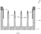
- FIG. 5 is a cross-section view of the partially completed semiconductor device 100 after deposition of a metal layer 128 over the second isolation material 124 , the upper portions of the semiconductor fins 102 a and 102 b and between the first and second isolation materials, 126 and 124 , respectively, according to an embodiment of the disclosure.
- the metal layer 128 may be deposited by ALD, CVD, PVD, electroplating or any suitable deposition processes.
- the metal layer 128 may be made of, but is not limited to, tungsten (W), ruthenium (Ru), titanium (Ti), or titanium nitride (TiN).
- the metal utilized for layer 128 should have thermal stability required to process through the semiconductor processing operations.
- the metal layer 128 may be deposited over upper surfaces of the second isolation material 124 .
- a planarization process such as CMP may be used to remove the metal layer 128 from the upper surfaces of the second isolation material 124 .
- FIG. 6A is a cross-section view of the partially completed semiconductor device 100 after removal of the metal layer 128 from the upper portions of the semiconductor fins 102 a and 102 b to form a metal structure 128 over the second isolation material 124 and between the first and second isolation materials, 126 and 124 , respectively, according to an embodiment of the disclosure.
- the removal of the metal layer 128 may be by wet etch or dry etch process.
- the second isolation material 124 , the protective nitride caps 104 and the spacer structures 122 protect the upper portions of the semiconductor fins 102 a and 102 b from the etching process.
- the second isolation material 124 may be removed from the spacer structures 122 and the protective nitride caps 104 .
- FIG. 6B is a cross-section view of the partially completed semiconductor device 100 taken along section line Y-Y′ of FIG. 6A , according to an embodiment of the disclosure.
- the metal layer 128 fills up the cavity in the lower portions of the semiconductor fins 102 a and 102 b .
- the cavity may be partially or fully filled.
- FIG. 6C is a corresponding top view of the partially completed semiconductor device 100 shown in FIGS. 6A and 6B , according to an embodiment of the disclosure. Portions of the semiconductor fins 102 a and 102 b underneath the nitride layer 112 are shown as dashed outlines. The metal structure 128 is formed over a portion of the substrate 110 that is not covered by the nitride layer 112 .
- FIG. 7A is a cross-section view of the partially completed semiconductor device 100 after deposition of a dielectric liner 130 over the upper portions of the semiconductor fins 102 a and 102 b and the metal structure 128 , formation of a second dielectric material 132 over the dielectric liner 130 and removal of the nitride layer 112 from the first dielectric material 106 to expose the first dielectric material 106 , according to an embodiment of the disclosure.
- the dielectric liner 130 and the second dielectric material 132 may be deposited by ALD, CVD, PVD or any other suitable deposition processes.
- the dielectric liner 130 may be made of silicon nitride.
- the second dielectric material 132 may be made of silicon dioxide.
- the dielectric liner 130 and the second dielectric material 132 may be deposited over upper surfaces of the nitride layer 112 .
- a planarization process such as CMP may be used to remove the dielectric liner 130 and the second dielectric material 132 from the upper surfaces of the nitride layer 112 and the nitride layer 112 from upper surfaces of the first dielectric material 106 .
- the planarization process may also remove the dielectric liner 130 from top surfaces of the semiconductor fins 102 a and 102 b.
- FIG. 7B is a cross-section view of the partially completed semiconductor device 100 taken along section line Y-Y′ of FIG. 7A , according to an embodiment of the disclosure.
- the nitride layer 112 may also be removed from portions of the semiconductor fins 102 to expose the protective nitride caps 104 .
- FIG. 8A is a cross-section view of the partially completed semiconductor device 100 after formation of an active region mask 134 over the upper portions of the semiconductor fins 102 a and 102 b , over the metal structure 128 and over the second dielectric material 132 and removal of portions of the first dielectric material 106 that are not covered by the active region mask 134 , according to an embodiment of the disclosure.
- the formation of the active region mask 134 may include depositing a layer of photoresist material on a top surface of the semiconductor device 100 , followed by conventional photoresist exposure and developing to form the required photoresist patterns. A wet etch or dry etch process may be used to remove portions of the first dielectric material 106 that are not covered by the photoresist patterns.
- FIG. 8B is a cross-section view of the partially completed semiconductor device 100 taken along section line Y-Y′ of FIG. 8A , according to an embodiment of the disclosure.
- portions of the semiconductor fins 102 a and 102 b that are not covered by the active region mask 134 may be removed by wet etch or dry etch process to define an active layer.
- the semiconductor fins 102 a and 102 b may extend over the metal structure 128 .
- the metal structure 128 may have sidewalls. A portion of the sidewall of the metal structure 128 may be covered by a lower portion of the semiconductor fins 102 a and 102 b .
- the lower portion of the semiconductor fins 102 a and 102 b may be separated from the portion of the sidewall of the metal structure 128 by the first isolation material 126 .
- FIG. 8C is a corresponding top view of the partially completed semiconductor device 100 shown in FIGS. 8A and 8B , according to an embodiment of the disclosure.
- the active region mask 134 defines the active layer of the semiconductor device 100 . Portions of the semiconductor fins 102 a and 102 b that are not covered by the active region mask 134 may be removed to expose the semiconductor substrate 110 .
- FIG. 9A is a cross-section view of the partially completed semiconductor device 100 after removal of the active region mask 134 and formation of a third dielectric material 136 over the etched portions of the first dielectric material 106 , according to an embodiment of the disclosure.
- the active region mask 134 may be removed by wet etch or dry etch process.
- the formation of the third dielectric material 136 may include depositing the third dielectric material 136 over the etched portions of the first dielectric material 106 .
- the third dielectric material 136 may also be deposited over upper surfaces of the second dielectric material 132 and over upper portions of the semiconductor fins 102 .
- the third dielectric material 136 may be deposited by CVD, PVD, ALD or any other suitable deposition processes.
- the third dielectric material 136 may be made of silicon dioxide. In an embodiment, the third dielectric material 136 may be STI. A planarization process such as CMP may be used to remove portions of the third dielectric material 136 from the upper surfaces of the second dielectric material 132 and from the upper portions of the semiconductor fins 102 a and 102 b.
- FIG. 9B is a cross-section view of the partially completed semiconductor device 100 taken along section line Y-Y′ of FIG. 9A , according to an embodiment of the disclosure.
- the third dielectric material 136 may also be deposited over the etched portions of the semiconductor fins 102 a and 102 b.
- FIG. 9C is a corresponding top view of the partially completed semiconductor device 100 shown in FIGS. 9A and 9B , according to an embodiment of the disclosure.
- the first and the second semiconductor fins, 102 a and 102 b respectively, have a length 170 .
- the metal structure 128 extends at least across the length 170 of the semiconductor fins 102 a and 102 b .
- the first and the second semiconductor fins 102 a and 102 b have a width 172 and are separated by a separation distance 176 .
- the metal structure 128 extends at least across the widths 172 of the fins 102 a and 102 b and the separation distance 176 between the fins 102 a and 102 b .
- the metal structure 128 under the active layer is depicted as a dashed outline.
- the metal structure 128 has a length and a width that are at least equal to or greater than the length and the width, respectively, of the active layer.
- FIG. 10 is a cross-section view of the partially completed semiconductor device 100 after removal of a portion of the second dielectric material 132 from the upper portions of the semiconductor fins 102 a and 102 b , removal of the protective nitride caps 104 from top surfaces of the semiconductor fins 102 a and 102 b , removal of the dielectric liner 130 from upper portions of the semiconductor fins 102 a and 102 b , removal of the dielectric spacers 122 from the upper portions of the semiconductor fins 102 a and 102 b and from sidewalls of the second dielectric material 132 and removal of upper portions of the third dielectric material 136 , according to an embodiment of the disclosure.
- the removal of the second dielectric material 132 , protective nitride caps 104 , dielectric liner 130 and dielectric spacers 122 exposes the upper portions of the semiconductor fins 102 a and 102 b .
- the second dielectric material 132 , protective nitride caps 104 , dielectric liner 130 , dielectric spacers 122 and the third dielectric material 136 may be removed by wet etch or dry etch process.
- FIG. 11A is a top view of the semiconductor device 100 after formation of gate electrodes 156 over the semiconductor fins 102 a and 102 b , epitaxial structures 138 on the semiconductor fins 102 a and 102 b and contacts 142 a , 142 b , 146 a and 146 b to the metal structure 128 , according to an embodiment of the disclosure.
- the metal structure 128 is depicted as a dashed outline.
- the gate electrodes 156 transverse the plurality of fins 102 a and 102 b.
- Formation of the gate electrodes 156 may include depositing a layer of amorphous silicon over the plurality of fins 102 a and 102 b .
- a layer of photoresist material may be deposited over the amorphous silicon layer followed by conventional photoresist exposure and developing to form photoresist patterns that are consistent with prior art practices.
- a wet etch or dry etch process may be used to remove portions of the amorphous silicon that are not covered by the photoresist patterns.
- the photoresist material is removed after the etching processes. Spacer structures may then be formed over the patterned amorphous silicon layer.
- the formation of the spacer structures may include depositing a layer of dielectric material over the patterned amorphous silicon layer followed by anisotropic etching of the dielectric material.
- Epitaxial structures 138 may be formed on exposed upper portions of the semiconductor fins 102 a and 102 b that are not covered by the patterned amorphous silicon layer and the spacer structures.
- the formation of the epitaxial structures 138 includes forming a cavity in the exposed upper portions of the fins 102 a and 102 b followed by growth of the epitaxial structures 138 in the fin cavity, consistent with prior art practices.
- a layer of interlayer dielectric (ILD) material may subsequently be deposited over the patterned amorphous silicon layer, the spacer structures and the epitaxial structures 138 followed by a planarization process such as CMP to remove the ILD material from upper surfaces of the patterned amorphous silicon layer and the spacer structures.
- the ILD material may be made of silicon dioxide and may be deposited by CVD or PVD.
- the patterned amorphous silicon layer may be removed by wet etch or dry etch process, exposing portions of the semiconductor fins 102 a and 102 b .
- Gate metal may be deposited over the exposed portions of the semiconductor fins 102 a and 102 b to form the gate electrodes 156 .
- FIG. 11B is a cross-section view of the semiconductor device 100 taken along section line X-X′ of FIG. 11A , according to an embodiment of the disclosure.
- a contact 142 a may be formed to electrically connect the metal structure 128 to the epitaxial structures 138 .
- the formation of the contact 142 a may include removing a portion of the ILD material 150 , the second dielectric material 132 and the dielectric liner 130 to form an opening exposing a portion of the metal structure 128 and the epitaxial structures 138 .
- a contact metal may subsequently be deposited into the opening.
- the removal of the ILD material 150 , the second dielectric material 132 and the dielectric liner 130 may be by wet etch or dry etch process.
- the contact metal may be deposited by ALD, CVD, PVD, electroplating or any other suitable deposition processes. In an embodiment, the contact metal may be W or cobalt (Co).
- FIG. 11C is a cross-section view of the semiconductor device 100 taken along section line X′-X′′ of FIG. 11A , according to an embodiment of the disclosure.
- a contact 142 b may be formed by etching the ILD material 150 to form an opening exposing the epitaxial structures 138 .
- a portion of the exposed epitaxial structures 138 may subsequently be removed followed by removal of the ILD material 150 , the second dielectric material 132 and the dielectric liner 130 to expose the metal structure 128 .
- a contact metal may subsequently be deposited in the opening.
- the removal of the epitaxial structures 138 may be by wet etch or dry etch process.
- FIG. 11D is a cross-section view of the semiconductor device 100 taken along section line Y-Y′ of FIG. 11A , according to an embodiment of the disclosure.
- contact 146 a may be disposed over a conductive trench silicide layer 180 , the trench silicide layer 180 being disposed over the metal structure 128 .
- Contact 146 b extends from the metal structure 128 to an upper surface of the ILD material 150 .
- the contacts 146 a and 146 b may be used to connect to upper metallization levels.
- FIG. 12 is a three-dimensional view of the semiconductor device 100 , according to an embodiment of the disclosure.
- the semiconductor device 100 comprises a substrate 110 and an active layer over the substrate 110 .
- the active layer comprises upper portions of the first and second semiconductor fins, 102 a and 102 b , respectively.
- epitaxial structures may be formed on the upper portions of the semiconductor fins 102 a and 102 b .
- the active layer may include the epitaxial structures disposed on the upper portions of the first and second semiconductor fins, 102 a and 102 b , respectively.
- the metal structure 128 is positioned between the active layer and the substrate 110 .
- the metal structure 128 extends at least across the widths 172 of the first and second semiconductor fins, 102 a and 102 b , respectively, and the separation distance 176 between the fins 102 a and 102 b .
- the first isolation material 126 separates the metal structure 128 from the active layer.
- the second isolation material 124 separates the metal structure 128 from the substrate 110 .
- a contact 152 may be formed over the epitaxial structures on the semiconductor fins 102 a and 102 b .
- a contact 142 may be formed to electrically connect the epitaxial structures to the metal structure 128 .
- Base portions 102 a ′ and 102 b ′ of the semiconductor fins, 102 a and 102 b , respectively, may be disposed on an upper surface of the substrate 110 .
- the metal structure 128 may separate the upper portions of the semiconductor fins 102 a and 102 b from the base portions of the semiconductor fins, 102 a ′ and 102 b ′, respectively.
- the second isolation material 124 may separate the base portions 102 a ′ and 102 b ′ of the semiconductor fins, 102 a and 102 b , respectively from the metal structure 128 .
- the length and the width of the metal structure 128 may be expanded for resistance optimization.
- the metal structure 128 is positioned between the substrate 110 and upper portions of the semiconductor fins 102 a and 102 b , therefore it does not lead to an increase in the semiconductor device 100 height. Placing the metal structure between the active layer and the substrate 110 instead of the BEOL metallization layers leads to improved pin access as well as signal routing between devices. As the metal structure is not placed in the BEOL metallization layers, the number of BEOL metallization stacks may be reduced resulting in a shorter semiconductor device 100 height.
- the metal structure 128 may also shield the active layer from electromagnetic radiation as well as injected light from the substrate side of the device.
- FIGS. 13 to 15 illustrate a fabrication process flow to form a cavity over the substrate for subsequent deposition of a metal structure according to another embodiment of the disclosure.
- the substrate may be a SOI layer.
- the same reference numbers used in FIGS. 1 to 4 are also used in FIGS. 13 to 15 for identical features.
- FIG. 13A is a cross-section view of a partially completed semiconductor device 200 , according to another embodiment of the disclosure.
- the semiconductor device 200 comprises a first semiconductor fin 102 a and a second semiconductor fin 102 b disposed over a substrate 110 .
- the semiconductor fins 102 a and 102 b are separated from the substrate 110 by a dielectric material 106 a .
- the dielectric material 106 a may be a bottom oxide layer of a SOI layer.
- a dielectric material 106 b may be deposited over the semiconductor fins 102 a and 102 b and the dielectric material 106 a followed by a planarization process such as CMP.
- the dielectric materials 106 a and 106 b may be collectively referred to as dielectric material 106 .
- the dielectric material 106 may be made of silicon dioxide.
- a nitride layer 112 may be deposited over the semiconductor fins 102 a and 102 b and the dielectric material 106 b followed by patterning using a bottom isolation mask layer 120 .
- FIG. 13B is a corresponding top view of the partially completed semiconductor device shown in FIG. 13A .
- the semiconductor fins 102 a and 102 b underneath the patterned nitride layer 112 are shown as dashed outlines.
- FIG. 14 is a cross-section view of a partially completed semiconductor device 200 after removal of the dielectric material 106 , according to another embodiment of the disclosure.
- the removal process forms a cavity in the dielectric material 106 a between the semiconductor fins 102 a and 102 b and the substrate 110 .
- the removal process may be by a wet or dry etch process.
- FIG. 15A is a cross-section view of a partially completed semiconductor device 200 after formation of a first isolation material 126 and a second isolation material 224 , according to another embodiment of the disclosure.
- the first isolation material 126 may be formed on bottom surfaces of the semiconductor fins 102 a and 102 b .
- the second isolation material 224 may be formed over the substrate 110 .
- the first isolation material 126 is made of silicon dioxide.
- the first isolation material 126 may be made by thermal oxidation or deposited by CVD, ALD or any other suitable methods.
- the second isolation material 224 may be made of silicon nitride.
- the second isolation material 224 may be deposited by CVD, ALD or any other suitable methods.
- FIG. 15B is a corresponding cross-section view of the partially completed semiconductor device 200 shown in FIG. 15A taken along section line Y-Y′, according to another embodiment of the disclosure.
- the first isolation material 126 is formed on the top surface of the cavity in the dielectric material 106 a .
- the second isolation material 224 is formed on the bottom surface and sidewalls of the cavity in the dielectric material 106 a .
- Subsequent process steps for the semiconductor device 200 fabrication are similar to the process flow for semiconductor device 100 shown in FIGS. 5 to 12 .
Landscapes
- Element Separation (AREA)
Abstract
Description
Claims (20)
Priority Applications (1)
| Application Number | Priority Date | Filing Date | Title |
|---|---|---|---|
| US16/784,256 US11217533B2 (en) | 2020-02-07 | 2020-02-07 | Semiconductor device with metal structure under an active layer |
Applications Claiming Priority (1)
| Application Number | Priority Date | Filing Date | Title |
|---|---|---|---|
| US16/784,256 US11217533B2 (en) | 2020-02-07 | 2020-02-07 | Semiconductor device with metal structure under an active layer |
Publications (2)
| Publication Number | Publication Date |
|---|---|
| US20210249352A1 US20210249352A1 (en) | 2021-08-12 |
| US11217533B2 true US11217533B2 (en) | 2022-01-04 |
Family
ID=77177066
Family Applications (1)
| Application Number | Title | Priority Date | Filing Date |
|---|---|---|---|
| US16/784,256 Active 2040-05-01 US11217533B2 (en) | 2020-02-07 | 2020-02-07 | Semiconductor device with metal structure under an active layer |
Country Status (1)
| Country | Link |
|---|---|
| US (1) | US11217533B2 (en) |
Families Citing this family (1)
| Publication number | Priority date | Publication date | Assignee | Title |
|---|---|---|---|---|
| US12543343B2 (en) | 2021-10-19 | 2026-02-03 | Taiwan Semiconductor Manufacturing Co., Ltd. | Semiconductor structure and method for forming the same |
Citations (6)
| Publication number | Priority date | Publication date | Assignee | Title |
|---|---|---|---|---|
| US9570395B1 (en) | 2015-11-17 | 2017-02-14 | Samsung Electronics Co., Ltd. | Semiconductor device having buried power rail |
| US20180145030A1 (en) | 2016-11-21 | 2018-05-24 | Imec Vzw | Integrated circuit chip with power delivery network on the backside of the chip |
| US20180233500A1 (en) * | 2017-02-13 | 2018-08-16 | International Business Machines Corporation | Fabrication of vertical field effect transistors with uniform structural profiles |
| US20180261540A1 (en) * | 2017-03-09 | 2018-09-13 | Samsung Electronics Co., Ltd. | Integrated circuit device |
| US20180374791A1 (en) | 2017-06-22 | 2018-12-27 | Tokyo Electron Limited | Buried power rails |
| WO2019009871A1 (en) | 2017-07-01 | 2019-01-10 | Intel Corporation | Metallization structures under a semiconductor device layer |
-
2020
- 2020-02-07 US US16/784,256 patent/US11217533B2/en active Active
Patent Citations (6)
| Publication number | Priority date | Publication date | Assignee | Title |
|---|---|---|---|---|
| US9570395B1 (en) | 2015-11-17 | 2017-02-14 | Samsung Electronics Co., Ltd. | Semiconductor device having buried power rail |
| US20180145030A1 (en) | 2016-11-21 | 2018-05-24 | Imec Vzw | Integrated circuit chip with power delivery network on the backside of the chip |
| US20180233500A1 (en) * | 2017-02-13 | 2018-08-16 | International Business Machines Corporation | Fabrication of vertical field effect transistors with uniform structural profiles |
| US20180261540A1 (en) * | 2017-03-09 | 2018-09-13 | Samsung Electronics Co., Ltd. | Integrated circuit device |
| US20180374791A1 (en) | 2017-06-22 | 2018-12-27 | Tokyo Electron Limited | Buried power rails |
| WO2019009871A1 (en) | 2017-07-01 | 2019-01-10 | Intel Corporation | Metallization structures under a semiconductor device layer |
Also Published As
| Publication number | Publication date |
|---|---|
| US20210249352A1 (en) | 2021-08-12 |
Similar Documents
| Publication | Publication Date | Title |
|---|---|---|
| US11935794B2 (en) | Method for forming long channel back-side power rail device | |
| KR102596378B1 (en) | Semiconductor device structure | |
| US7183624B2 (en) | Semiconductor device | |
| JP2022159383A (en) | Three-dimensional memory device and method | |
| KR101791752B1 (en) | Stacked device and associated layout structure | |
| US11621332B2 (en) | Wraparound contact to a buried power rail | |
| US9559000B1 (en) | Hybrid logic and SRAM contacts | |
| US8623727B2 (en) | Method for fabricating semiconductor device with buried gate | |
| US10763262B2 (en) | Method of preparing semiconductor structure | |
| KR20130039525A (en) | Semiconductor device with damascene bitline and method for fabricating the same | |
| KR20100088836A (en) | Method of manufacturing a semiconductor device | |
| US12616019B2 (en) | Via connection to backside power delivery network | |
| KR20190064514A (en) | Buried metal for finfet device and method | |
| TW202243202A (en) | Complementary metal oxide semiconductor device | |
| US20070075366A1 (en) | Semiconductor memory device and method for manufacturing the same | |
| TWI798796B (en) | Semiconductor device with carbon liner over gate structure and method for forming the same | |
| US11217533B2 (en) | Semiconductor device with metal structure under an active layer | |
| US11888038B2 (en) | Integrated circuit devices and methods of manufacturing the same | |
| US20250285975A1 (en) | Enhanced power rail connection | |
| US20240290714A1 (en) | Three-dimensional memory device containing multi-level word line contact wells and methods for manufacturing the same | |
| US20090086523A1 (en) | Integrated circuit and method of forming an integrated circuit | |
| KR100945508B1 (en) | Zero Capacitor Ram and Method of Manufacturing the Same | |
| US10269812B1 (en) | Forming contacts for VFETs | |
| US12080588B2 (en) | Buried metal for FinFET device and method | |
| US20250364408A1 (en) | Semiconductor device including through via and method of making |
Legal Events
| Date | Code | Title | Description |
|---|---|---|---|
| AS | Assignment |
Owner name: GLOBALFOUNDRIES INC., CAYMAN ISLANDS Free format text: ASSIGNMENT OF ASSIGNORS INTEREST;ASSIGNORS:SOSS, STEVEN ROBERT;BENTLEY, STEVEN JOHN;FROUGIER, JULIEN;SIGNING DATES FROM 20200131 TO 20200206;REEL/FRAME:051747/0195 |
|
| FEPP | Fee payment procedure |
Free format text: ENTITY STATUS SET TO UNDISCOUNTED (ORIGINAL EVENT CODE: BIG.); ENTITY STATUS OF PATENT OWNER: LARGE ENTITY |
|
| AS | Assignment |
Owner name: GLOBALFOUNDRIES U.S. INC., CALIFORNIA Free format text: ASSIGNMENT OF ASSIGNORS INTEREST;ASSIGNOR:GLOBALFOUNDRIES INC.;REEL/FRAME:054633/0001 Effective date: 20201022 |
|
| AS | Assignment |
Owner name: GLOBALFOUNDRIES U.S. INC., NEW YORK Free format text: RELEASE BY SECURED PARTY;ASSIGNOR:WILMINGTON TRUST, NATIONAL ASSOCIATION;REEL/FRAME:056987/0001 Effective date: 20201117 Owner name: GLOBALFOUNDRIES U.S. INC., NEW YORK Free format text: RELEASE OF SECURITY INTEREST;ASSIGNOR:WILMINGTON TRUST, NATIONAL ASSOCIATION;REEL/FRAME:056987/0001 Effective date: 20201117 |
|
| STPP | Information on status: patent application and granting procedure in general |
Free format text: NON FINAL ACTION MAILED |
|
| STPP | Information on status: patent application and granting procedure in general |
Free format text: RESPONSE TO NON-FINAL OFFICE ACTION ENTERED AND FORWARDED TO EXAMINER |
|
| STPP | Information on status: patent application and granting procedure in general |
Free format text: NOTICE OF ALLOWANCE MAILED -- APPLICATION RECEIVED IN OFFICE OF PUBLICATIONS |
|
| STPP | Information on status: patent application and granting procedure in general |
Free format text: PUBLICATIONS -- ISSUE FEE PAYMENT RECEIVED |
|
| STPP | Information on status: patent application and granting procedure in general |
Free format text: PUBLICATIONS -- ISSUE FEE PAYMENT VERIFIED |
|
| STCF | Information on status: patent grant |
Free format text: PATENTED CASE |
|
| MAFP | Maintenance fee payment |
Free format text: PAYMENT OF MAINTENANCE FEE, 4TH YEAR, LARGE ENTITY (ORIGINAL EVENT CODE: M1551); ENTITY STATUS OF PATENT OWNER: LARGE ENTITY Year of fee payment: 4 |