US11216722B2 - Hardware accelerator template and design framework for implementing recurrent neural networks - Google Patents
Hardware accelerator template and design framework for implementing recurrent neural networks Download PDFInfo
- Publication number
- US11216722B2 US11216722B2 US15/396,520 US201615396520A US11216722B2 US 11216722 B2 US11216722 B2 US 11216722B2 US 201615396520 A US201615396520 A US 201615396520A US 11216722 B2 US11216722 B2 US 11216722B2
- Authority
- US
- United States
- Prior art keywords
- accelerator
- matrix
- vector
- operations
- rnn
- Prior art date
- Legal status (The legal status is an assumption and is not a legal conclusion. Google has not performed a legal analysis and makes no representation as to the accuracy of the status listed.)
- Active, expires
Links
Images


Classifications
-
- G—PHYSICS
- G06—COMPUTING OR CALCULATING; COUNTING
- G06N—COMPUTING ARRANGEMENTS BASED ON SPECIFIC COMPUTATIONAL MODELS
- G06N3/00—Computing arrangements based on biological models
- G06N3/02—Neural networks
- G06N3/06—Physical realisation, i.e. hardware implementation of neural networks, neurons or parts of neurons
- G06N3/063—Physical realisation, i.e. hardware implementation of neural networks, neurons or parts of neurons using electronic means
-
- G—PHYSICS
- G06—COMPUTING OR CALCULATING; COUNTING
- G06N—COMPUTING ARRANGEMENTS BASED ON SPECIFIC COMPUTATIONAL MODELS
- G06N3/00—Computing arrangements based on biological models
- G06N3/02—Neural networks
- G06N3/04—Architecture, e.g. interconnection topology
- G06N3/044—Recurrent networks, e.g. Hopfield networks
- G06N3/0442—Recurrent networks, e.g. Hopfield networks characterised by memory or gating, e.g. long short-term memory [LSTM] or gated recurrent units [GRU]
-
- G06N3/0445—
-
- G—PHYSICS
- G06—COMPUTING OR CALCULATING; COUNTING
- G06N—COMPUTING ARRANGEMENTS BASED ON SPECIFIC COMPUTATIONAL MODELS
- G06N3/00—Computing arrangements based on biological models
- G06N3/02—Neural networks
- G06N3/04—Architecture, e.g. interconnection topology
- G06N3/0495—Quantised networks; Sparse networks; Compressed networks
Definitions
- the disclosure relates generally to electronics, and, more specifically, embodiments relating to hardware accelerator templates and design frameworks for implementing recurrent neural networks and variants thereof.
- Neural networks which is an umbrella term including many diverse models and approaches, are a type of artificial intelligence that attempts to imitate the way a human brain works. Neural networks, at their core, work by creating connections between nodes, the computer equivalent of neurons. The organization and weights of the connections determine the output. One key feature of a neural network is that it has an ability to learn. Thus, neural networks are not just complex systems but are adaptive systems that can change their internal structure based on the information that flows through it—typically using weights.
- FIG. 1 is a block diagram illustrating a RNN 100 and an unrolled recurrent neural network 150 .
- the RNN 100 includes an input value (I t ) 102 , a node 104 (sometimes referred to as a neuron, etc.) that is executed a number of times via the recurrent connection 105 , and an output value (O t ) 106 .
- RNNs within the node 104 , typically perform a variety operations; commonly, these are matrix operations and/or vector operations (e.g., a dense matrix*vector, or vector-wise add, multiply, hyperbolic tangent, sigmoid, etc.).
- matrix operations e.g., a dense matrix*vector, or vector-wise add, multiply, hyperbolic tangent, sigmoid, etc.
- RNNs are especially useful in analyzing sequences of data. While a typical feedforward (or non-recurrent) neural network produces its output solely based on its current input, an RNN 100 produces its output by considering not only its current input 102 , but also based on the history of its previous inputs and/or outputs.
- RNNs are currently utilized to provide state-of-the-art results in many applications, e.g., in language modeling.
- the “unrolled” (or expanded) RNN 150 shows how multiple iterations (or copies of a node 104 ) can use multiple input values 152 A- 152 D can be used to generate an output value 154 .
- the input values 152 A- 152 D are a sequence of words, and the RNN 150 can output a predicted next word in the sequence, a probability for a next word in the sequence, etc.
- Such predictions are particularly useful in various applications such as sentence completion, speech recognition, sentiment analysis, machine translation, etc.
- the input values 152 A- 152 D are a 3-word sequence for a sentence “a week has seven”, which is provided to the RNN 150 , which analyzes its inputs on a word-by-word basis, and ultimately predicts that the next word for the sentence is “days”.
- RNNs one of the appeals of RNNs is that they can make use of “context” via previous information, which can be applied it to a present task, such as using previous words in a sentence to assist in determining what a next word might be.
- neural networks are to solve problems similar to how a human brain would.
- most modern neural network implementations typically utilize a few thousand to a few million neural units and millions of connections or more. Accordingly, the training and use of such networks is extremely computationally expensive, requiring substantial requirements in terms of processing, memory, bandwidth, etc.
- FIG. 1 is a block diagram illustrating a recurrent neural network and an unrolled recurrent neural network.
- FIG. 2 is a block diagram illustrating exemplary compositions of a standard recurrent neural network, a gated recurrent unit variant, and a long short term memory variant.
- FIG. 3 is a diagram illustrating a composition of matrix and vector operations for implementing a gated recurrent unit variant.
- FIG. 4 is a block diagram illustrating an exemplary design framework and top-level architecture of a hardware accelerator template according to some embodiments.
- FIG. 5 is a block diagram illustrating a table of customizable parameters of a hardware accelerator template and a table of auto-tuning factors according to some embodiments.
- FIG. 6 is a block diagram illustrating matrix processing unit customizations, including a matrix multiplication, a matrix processing unit using six floating-point-multiple add units, and a matrix processing unit using twelve floating-point-multiple add units according to some embodiments.
- FIG. 7 is a block diagram illustrating exemplary programming for a pipelined gated recurrent unit computation according to some embodiments.
- FIG. 8 is a flow diagram illustrating a flow of operations for generating an accelerator instance to implement a recurrent neural network according to some embodiments.
- FIG. 9 illustrates an exemplary implementation in which an accelerator is communicatively coupled to a plurality of cores through a cache coherent interface according to some embodiments.
- FIG. 10 illustrates another view of an accelerator according to some embodiments.
- FIG. 11 illustrates an exemplary set of operations performed by the processing elements according to some embodiments.
- FIG. 12 a depicts an example of a multiplication between a sparse matrix A against a vector x to produce a vector y according to some embodiments.
- FIG. 12 b illustrates the CSR representation of matrix A in which each value is stored as a (value, row index) pair according to some embodiments.
- FIG. 12 c illustrates a CSC representation of matrix A which uses a (value, column index) pair according to some embodiments.
- FIGS. 13 a , 13 b , and 13 c illustrate pseudo code of each compute pattern, in which:
- FIG. 13 a illustrates a row-oriented sparse matrix dense vector multiply (spMdV_csr) according to some embodiments.
- FIG. 13 b illustrates a column-oriented sparse matrix sparse vector multiply (spMspC_csc) according to some embodiments.
- FIG. 13 c illustrates a scale and update operation (scale_update) according to some embodiments.
- FIG. 14 illustrates the processing flow for one implementation of the data management unit and the processing elements according to some embodiments.
- FIG. 15 a highlights paths for spMspV_csc and scale_update operations according to some embodiments.
- FIG. 15 b illustrates paths for a spMdV_csr operation according to some embodiments.
- FIG. 16 a shows an example graph.
- FIG. 16 b shows an example of representing the graph of FIG. 16 a as an adjacency matrix.
- FIG. 16 c illustrates a vertex program according to some embodiments.
- FIG. 16 d illustrates exemplary program code for executing a vertex program according to some embodiments.
- FIG. 16 e shows a generalized sparse matrix vector multiply (GSPMV) formulation according to some embodiments.
- FIG. 17 illustrates one implementation of a design framework for GSPMV according to some embodiments.
- FIG. 18 shows one implementation of an architecture template for GSPMV according to some embodiments.
- FIG. 19 illustrates a summarization of the operation of each accelerator tile according to some embodiments.
- FIG. 20 a illustrates a table summarizing the customizable parameters of one implementation of the template according to some embodiments.
- FIG. 20 b illustrates tuning considerations of one implementation of the framework that performs automatic tuning to determine the best design parameters to use to customize the hardware architecture template in order to optimize it for the input vertex program and (optionally) graph data according to some embodiments.
- FIG. 21 illustrates the compressed row storage (CRS, sometimes abbreviated CSR) sparse-matrix format according to some embodiments.
- CRS compressed row storage
- FIG. 22 shows exemplary steps involved in an implementation of sparse matrix-dense vector multiplication using the CRS data format according to some embodiments.
- FIG. 23 illustrates one implementation of an accelerator includes an accelerator logic die and one of more stacks of DRAM die according to some embodiments.
- FIG. 24 illustrates one implementation of the accelerator logic chip, oriented from a top perspective through the stack of DRAM die according to some embodiments.
- FIG. 25 provides a high-level overview of a dot-product engine (DPE) which contains two buffers, two 64-bit multiply-add arithmetic logic units (ALUs), and control logic according to some embodiments.
- DPE dot-product engine
- FIG. 26 illustrates a blocking scheme for large sparse-matrix computations according to some embodiments.
- FIG. 27 illustrates a format of block descriptors according to some embodiments.
- FIG. 28 illustrates the use of block descriptors for a two-row matrix that fits within the buffers of a single dot-product engine, on a system with only one stacked dynamic random access memory (DRAM) data channel and four-word data bursts, according to some embodiments.
- DRAM dynamic random access memory
- FIG. 29 illustrates one implementation of the hardware in a dot-product engine according to some embodiments.
- FIG. 30 illustrates the contents of the match logic unit that does capturing according to some embodiments.
- FIG. 31 shows the details of a dot-product engine design to support sparse matrix-sparse vector multiplication according to some embodiments.
- FIG. 32 illustrates an example multi-pass approach using specific values according to some embodiments.
- FIG. 33 shows how the sparse-dense and sparse-sparse dot-product engines described above can be combined according to some embodiments.
- FIG. 34 is a block diagram of a register architecture according to one embodiment of the invention.
- FIG. 35A is a block diagram illustrating both an exemplary in-order pipeline and an exemplary register renaming, out-of-order issue/execution pipeline according to embodiments of the invention
- FIG. 35B is a block diagram illustrating both an exemplary embodiment of an in-order architecture core and an exemplary register renaming, out-of-order issue/execution architecture core to be included in a processor according to embodiments of the invention;
- FIGS. 36A-B illustrate a block diagram of a more specific exemplary in-order core architecture, which core would be one of several logic blocks (including other cores of the same type and/or different types) in a chip;
- FIG. 36A is a block diagram of a single processor core, along with its connection to the on-die interconnect network and with its local subset of the Level 2 (L2) cache, according to embodiments of the invention;
- FIG. 36B is an expanded view of part of the processor core in FIG. 36A according to embodiments of the invention.
- FIG. 37 is a block diagram of a processor that may have more than one core, may have an integrated memory controller, and may have integrated graphics according to embodiments of the invention;
- FIGS. 38-41 are block diagrams of exemplary computer architectures
- FIG. 38 shown a block diagram of a system in accordance with one embodiment of the present invention.
- FIG. 39 is a block diagram of a first more specific exemplary system in accordance with an embodiment of the present invention.
- FIG. 40 is a block diagram of a second more specific exemplary system in accordance with an embodiment of the present invention.
- FIG. 41 is a block diagram of a SoC in accordance with an embodiment of the present invention.
- FIG. 42 is a block diagram contrasting the use of a software instruction converter to convert binary instructions in a source instruction set to binary instructions in a target instruction set according to embodiments of the invention.
- RNNs recurrent neural networks
- numerous specific details such as logic implementations, types and interrelationships of system components, etc., may be set forth in order to provide a more thorough understanding of some embodiments. It will be appreciated, however, by one skilled in the art that the invention may be practiced without such specific details. In other instances, control structures, gate level circuits, and/or full software instruction sequences have not been shown in detail in order not to obscure the invention. Those of ordinary skill in the art, with the included descriptions, will be able to implement appropriate functionality without undue experimentation.
- references in the specification to “one embodiment,” “an embodiment,” “an example embodiment,” etc., indicate that the embodiment described may include a particular feature, structure, or characteristic, but every embodiment may not necessarily include the particular feature, structure, or characteristic. Moreover, such phrases are not necessarily referring to the same embodiment. Further, when a particular feature, structure, or characteristic is described in connection with an embodiment, it is submitted that it is within the knowledge of one skilled in the art to affect such feature, structure, or characteristic in connection with other embodiments whether or not explicitly described.
- Bracketed text and blocks with dashed borders may be used herein to illustrate optional operations that add additional features to embodiments of the invention. However, such notation should not be taken to mean that these are the only options or optional operations, and/or that blocks with solid borders are not optional in certain embodiments of the invention.
- matrix processing units 464 A- 464 M include both “A” and “M” letter suffixes, which means that there could be one matrix processing unit, two matrix processing units, sixteen matrix processing units, etc.
- dashed lines e.g., matrix processing unit 464 M, vector processing unit 470 N
- the use of different letter characters as reference suffixes for different entities is not meant to indicate that there must be different numbers of these entities.
- the vector processing units 470 A- 470 N and the matrix processing units 464 A- 464 M include different letter suffixes—i.e., “N” and “M”—there could be the same number (or different numbers) of these in various embodiments.
- the use of the same letter character as a reference suffix for different entities is not meant to indicate that there must be the same numbers of these entities, although there could be in some embodiments.
- FIG. 2 is a block diagram illustrating exemplary compositions of a standard RNN 200 , a gated recurrent unit (GRU) variant 210 , and a long short term memory (LSTM) variant 220 .
- GRU gated recurrent unit
- LSTM long short term memory
- the standard RNN 200 includes of a fully connected tan h( ) layer with recurrent connections. It accepts as inputs: (1) data at step t, I t , and (2) the output of previous step O t-1 .
- the values W and U are dense matrices containing the neural network weights, whereas I t and O t-1 are represented as dense vectors.
- the standard RNN 200 provides fixed weights between the current input (I t ) and the previous history (O t-1 ) in producing the current output (O t ), which tends to “forget” information from a much earlier part of the input sequence, making the standard RNN 200 ineffective in learning long-term dependencies.
- GRU Gated Recurrent Unit
- LSTM Long Short Term Memory
- a GRU 210 or LSTM 220 have the ability to dynamically adjust the weights on current input and a history to determine how much long-term history to keep and the new information to carry forward.
- Equations are also illustrated in FIG. 2 along with the node part of the standard RNN 200 , GRU 210 , and LSTM 220 . These equations can thus “define” the particular network, and represent how the output (O t ) is to be determined based upon the inputs.
- the standard RNN 200 has one such equation
- GRU 210 has four equations
- LSTM 220 has six such equations.
- the four equations of GRU 210 are for an update gate, a reset gate, a new memory content, and a final memory content.
- each node being dependent upon the output of a previous node, it is also notable that in the case of GRU 210 and LSTM 220 , there are data dependencies between some of these equations, and thus, certain equations require the use of the output of other equations within the same node.
- the equation for N t utilizes both f t and i t , which are the outputs of other equations. Accordingly, due to these inter-node and intra-node data dependencies, the use of these types of networks can be computationally “expensive” as they are not easily implemented in a parallelizable manner.
- RNN unit
- GRU global resource unit
- LSTM LSTM
- AF activation functions
- RNNs are typically compositions of matrix and/or vector operations.
- RNNs at its core an RNN is composed of matrix and vector operations with data dependencies among them.
- FIG. 3 illustrates the GRU computation as a composition of matrix and vector operations.
- the “inputs” include a “regular” input value 304 of x t (e.g., I t of previous figures) and an output value 302 from a previous node of h t-1 (e.g., O t of previous figures), and each box with an M (e.g., M1, M2, etc.) represents a matrix operation to be performed, where each box with a V (e.g., V1, V2, V3) represents a vector operation.
- FIG. 3 shows a visual representation of a “flow graph” of the sets of operations, the involved operands, and the dependencies between data to perform a GRU computation.
- the x t and h t-1 can be used to determine the value of r t (via r t computation 310 ), which then is used in part to determine the value of ⁇ h t (via ⁇ h t computation 320 ), which is used along with the determined value of z t (via z t computation 340 ) to determine the value of h t (via h t computation 330 ).
- the RNN variants may dictate the sizes and types of the matrix and vector operations, as well as their data dependencies.
- matrix and vector sizes can be related to the number of hidden units in the RNN, and the activation function (AF) type (tan h, sigmoid, etc.) can relate to the type of vector operations.
- AF activation function
- embodiments disclosed herein provide a design framework that can be based on a customizable and programmable RNN hardware accelerator architecture template to enable automated development of RNN hardware accelerator instances that are specialized to meet user-provided sets of design constraints and goals while being flexible through programmability to execute arbitrary RNN variants.
- some embodiments enable customizable and programmable hardware accelerator instances for RNNs that can deliver extreme execution efficiency, while being able to flexibility execute arbitrary RNNs.
- the hardware accelerator instances can be deployed using a variety of types of hardware, including but not limited to Field Programmable Gate Arrays (FPGAs) as well as Application-Specific Integrated Circuits (ASICs).
- FPGAs Field Programmable Gate Arrays
- ASICs Application-Specific Integrated Circuits
- some embodiments can produce an accelerator instance optimized for a target FPGA chip with a particular number of hardware multiply and on-chip RAM resources, and some embodiments can produce an accelerator instance optimized for an ASIC for a particular market segment, programmable to support all RNN applications in this segment.
- the accelerator instance comprises RTL code
- the RTL code can be used as an input for a standard ASIC developmental tool (e.g., a logic synthesis tool) to generate an ASIC design.
- each accelerator instance is programmable.
- the accelerator itself can be programmed to support execution of arbitrary RNN variants.
- the framework can be configured to generate more efficient fixed-control units within the accelerator at the cost of programmability.
- embodiments enable the creation of RNN accelerators that can flexibly execute a wide range of RNN variants with optimal execution efficiency for the user-provided design constraints and goals.
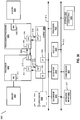
- FIG. 4 is a block diagram illustrating an exemplary design framework 400 and top-level architecture of a hardware accelerator template 450 according to some embodiments.
- the design framework 400 is shown as including a template mapping module 404 , a validation module 410 , and an automatic-tuning 416 module.
- the design framework 400 can be, for example, a software application that is executed by one or more computing devices. In some embodiments, one or more of these modules are not implemented or used.
- the design framework 400 includes the template mapping module 404 but not the validation module 410 or automatic-tuning 416 module; in other embodiments, the design framework 400 includes the template mapping module 404 and the validation module 410 , but not the automatic-tuning 416 module.
- the design framework 400 can take hardware (HW) design constraints 402 as an input.
- the HW design constraints 402 can specify what hardware should or should not be included (or utilized) by the resultant accelerator instance 406 .
- the HW design constraints 402 can include constraints such as a number of hardware multiply and adder resources to use, a number of pipeline stages in the multiply and adder units to use, available memory bandwidths, the type and/or amounts of on-chip RAMs, etc.
- the design framework 400 utilizes optimization goal inputs 408 , such as latency, throughput, power use, required layout area, etc., as inputs, which can be used when making design instances for the accelerator instance to meet the goals of the particular user.
- optimization goal inputs 408 such as latency, throughput, power use, required layout area, etc.
- the design framework 400 utilizes inputs such as a specification 414 of the particular RNN architecture targets, such as range of hidden unit sizes, type of activation functions (AFs), etc.
- these inputs are not used, but in others they are used and allow the generated accelerator instances to be specialized based on their target RNN applications.
- the inputs can include dataset properties 415 , such as the acceptable data types (e.g., float, double), expected lengths of input sequences, type of compression techniques amenable to the data, etc. This also is used in some embodiments but not in others, but its inclusion can allow the generated accelerator instances to be specialized to their target datasets.
- the framework 400 module can perform automatic tuning (via automatic tuning module 416 ) to explore the design space to determine an optimal set of customization parameters to be used in the design.
- FIG. 5 is a block diagram illustrating a table 500 of customizable parameters of a hardware accelerator template and a table 550 of auto-tuning factors according to some embodiments.
- these parameters 502 can be applied to a customizable hardware template for RNN accelerator architecture, which will be detailed below.
- tuning considerations can be utilized, such as the RNN unit types (e.g., standard RNN, GRU, LTSM), RNN architecture parameters (e.g., number of layers, sizes of hidden layers), dataset properties (e.g., sizes, distribution of values), optimization goals (e.g., latency, throughput), and/or design constraints (e.g., how many multiply units, random access memories (RAMs)).
- RNN unit types e.g., standard RNN, GRU, LTSM
- RNN architecture parameters e.g., number of layers, sizes of hidden layers
- dataset properties e.g., sizes, distribution of values
- optimization goals e.g., latency, throughput
- design constraints e.g., how many multiply units, random access memories (RAMs)
- the second column 554 shows what parameters of the hardware accelerator template may be affected by the tuning considerations 552 , such as the amount or configuration of various hardware blocks, e.g., matrix processing units (MPUs), vector processing units (VPUs), scratchpads (SPADs), data management units (DMUs), caches, pack/unpack units, etc.
- MPUs matrix processing units
- VPUs vector processing units
- SPADs scratchpads
- DMUs data management units
- caches e.g., pack/unpack units, etc.
- framework 400 module can include a template mapping module 404 that produces a customized accelerator instance (e.g., such as synthesizable register transfer language (RTL) utilizing a hardware description language (HDL) such as Verilog, VHDL, etc.) of the hardware accelerator that best meets the input constraints 402 and optimization goals 408 .
- a customized accelerator instance e.g., such as synthesizable register transfer language (RTL) utilizing a hardware description language (HDL) such as Verilog, VHDL, etc.
- HDL hardware description language
- the framework 400 module also generates a compiler to program the accelerator, e.g., via providing micro-code executed by control units, as described further herein.
- the framework 400 module in some embodiments also performs validations (via validation module 410 ), which includes comparing the generated accelerator instance (e.g., RTL) against reference functional and cycle-level performance models derived from the provided inputs constraints 402 /goals 408 . This validation checks for functional correctness, as well as whether the design meets the expected performance.
- validation module 410 includes comparing the generated accelerator instance (e.g., RTL) against reference functional and cycle-level performance models derived from the provided inputs constraints 402 /goals 408 . This validation checks for functional correctness, as well as whether the design meets the expected performance.
- the template mapping module 404 can map the design constraints 402 , subject to the optimization goals 408 and/or RNN specs 414 and/or dataset properties 415 if they exist, to a hardware accelerator template.
- the hardware accelerator template 450 includes one or more matrix processing units 464 A- 464 M (MPUs), which includes one or more floating-point multiply-accumulate units 466 (FMAs, also sometimes called floating-point multiply-add units) and an MPU control unit 468 .
- MPUs matrix processing units 464 A- 464 M
- FMAs floating-point multiply-accumulate units 466
- MPU control unit 468 MPU control unit 468 .
- the hardware accelerator template 450 also includes one or more vector processing units 470 A- 470 N (VPUs), which includes one or more FMAs 472 and/or one or more activation function blocks (for performing needed activation functions efficiently in hardware) and a VPU control unit 474 .
- VPUs vector processing units 470 A- 470 N
- the MPUs 464 A- 464 M and VPUs 470 A- 470 N may be directly connected (as shown by arrows 490 ) to allow the MPUs 464 A- 464 M and VPUs 470 A- 470 N to pass computed data between the two, thus reducing delay due to data dependencies that would be introduced in other systems.
- the hardware accelerator template 450 also includes one or more data management units (DMUs) 454 A- 454 Z to handle data movements in and out of the accelerator, each of which can include one or more scratchpads (SPADs) 456 and caches ($) 458 .
- DMUs data management units
- SPADs scratchpads
- caches ($) 458 .
- the scratchpads can be used to keep the matrix and vector data on-chip for the MPUs and VPUs to process.
- the scratchpads can be multi-banked/multi-ported accordingly to deliver the necessary bandwidth to feed the need for the MPUs and VPUs.
- the cache can optionally be used to take advantage of data locality. For example, in applications that accept word sequences as inputs, certain words can occur more often than others. Thus, it is beneficial to cache the vector representations of these frequent words to avoid accessing them from outside of the accelerator each time they are encountered.
- the DMUs also includes a pack/unpack unit 462 for handling various data formats, e.g., 32-bit double, 16-bit float, N-bit custom, and/or for processing compressed data, such as compressed representations of matrices.
- a pack/unpack unit 462 for handling various data formats, e.g., 32-bit double, 16-bit float, N-bit custom, and/or for processing compressed data, such as compressed representations of matrices.
- the MPU, VPU, and/or DMU includes control units (MPU control unit 468 , VPU control unit 474 , DMU control unit 460 ) that are based on programmable micro-codes. These units can orchestrate the operations among the MPUs, VPUs, and DMU to facilitate certain composition of matrix and vector operation executions. Thus, these control units can control the flow of data and processing of data within the accelerator to perform the desired RNN.
- the hardware accelerator template 450 can be viewed as a description of components that can be used in a physical hardware accelerator, in which particular component numbers, types, and/or arrangements can be determined by the template mapping module 404 (e.g., based upon the hardware design constraints 402 , optimization goals 408 , RNN specs, and/or dataset properties) to result in a custom, optimized hardware accelerator design that is specific to a particular application.
- the template parameters table 500 shows customization parameters of the template that can be utilized, in which various blocks are shown in column 502 .
- the architecture contains a set of matrix and vector processing units (MPUs, VPUs) that are customizable to handle a variety of design constraints/goals (e.g., to target certain matrix/vector sizes, adder/multiplier designs, amount of on-chip RAMs).
- MPUs, VPUs matrix and vector processing units
- Column 504 illustrates exemplary parameters of the blocks that can be modified; of course, this set is merely exemplary and other parameters (and blocks) can be utilized in various embodiments (and selected by those of ordinary skill in the art) without departing from the scope of the invention.
- FIG. 6 shows an example of how a 6 ⁇ 4 matrix multiplication (shown as 600 ) can be mapped to two possible customized MPUs that use six floating-point multiply-and-add (FMA) units (as 625 ) and twelve FMA units (as 650 ).
- FMA floating-point multiply-and-add
- the 6 ⁇ 4 matrix multiplication (shown as 600 ) illustrates how an input vector (VecIn) can be multiplied against a matrix having 6 rows and 4 columns, to result in an output vector (VecOut). As shown, the 6 rows can be split into two grouping: rows 0-2, and rows 3-5.
- the first customizable MPU 625 can implement this multiplication 600 using 6 FMAs, each of which operates upon a full row of the matrix to generate one value of the result vector (VecOut).
- the second customizable MPU 650 can implement the multiplication 600 using 12 FMAs, where groupings of two FMAs will together generate one value of the output vector by each working on two values from a row, instead of working on four values from a row, to together generate one value of the result vector (VecOut).
- this design can execute the 6 ⁇ 4 matrix multiplication faster (than the 6 FMA design 625 ), but at the expense of requiring more hardware resources, layout size, power, etc.
- the first design 625 could be selected when a constraint 402 or goal 408 causes a desire for fewer hardware blocks to be utilized, whereas the second design 650 could be selected when a constraint 402 or goal 408 causes a desire for optimal performance to be implemented.
- control units can be based on programmable micro-codes to orchestrate the operations among the MPUs, VPUs, and DMU to facilitate certain composition of matrix and vector operation executions for the RNN.
- FIG. 7 is a block diagram illustrating an example of how an accelerator instance with 2 VPUs, 1 MPU, and 1 DMU could be programmed to execute the GRU 210 computation illustrated in FIG. 2 .
- Each box in the figure is a micro-code command executed by the corresponding DMU 702 , MPU 704 , or VPUs 706 / 708 that is shown above it.
- the first box for the DMU 702 is a “load” command of row 0 from matrix 1.
- the lines connecting the boxes show data dependencies.
- Each micro-code command is executed when its dependencies have been resolved.
- the micro-codes are produced by a compiler for the accelerator (as described above with regard to FIG. 4 ), which can take as inputs the RNN architecture specifications 414 , optimization goals 408 , and/or dataset properties 415 .
- embodiments provide a design framework for automated—as opposed to manual—development (e.g., tuning, optimization, validation) of hardware accelerators to efficiently implement RNNs.
- FIG. 8 is a flow diagram illustrating a flow 800 of operations for generating an accelerator instance to implement a recurrent neural network according to some embodiments.
- this flow 600 is performed by the design framework module 400 of FIG. 4 .
- Flow 800 includes, at block 805 , obtaining a flow graph for a recurrent neural network (RNN) algorithm.
- the flow graph identifies a plurality of operations to be performed to implement the RNN algorithm and further identifies data dependencies between ones of the plurality of operations.
- the plurality of operations includes one or more matrix operations and one or more vector operations.
- block 805 includes block 810 , which includes computing the flow graph based upon a plurality of equations corresponding to the RNN algorithm.
- Flow 800 also includes, at block 815 , mapping the plurality of operations of the flow graph to an accelerator hardware template to yield the accelerator instance comprising register transfer language code that describes how one or more matrix processing units (MPUs) and one or more vector processing units (VPUs) are to be arranged to perform the RNN algorithm. At least one of the one or more MPUs, as part of implementing the RNN algorithm, is to directly provide or directly receive a value from one of the one or more VPUs.
- MPUs matrix processing units
- VPUs vector processing units
- block 815 includes block 820 , where the mapping is based upon hardware design constraints indicating amounts or capabilities of hardware elements that can be utilized in the accelerator instance.
- block 815 includes block 825 , where the mapping is based upon optimization goals indicating properties of the accelerator instance that should be optimized for.
- block 815 includes block 830 , where the mapping is based upon one or more dataset properties identifying properties of the input data to be used with the accelerator instance.
- block 815 includes block 835 , where the mapping further yields a compiler that is executable to program an accelerator, generated based upon the accelerator instance, to execute micro-code to implement the RNN algorithm.
- a method in a design framework module implemented by an electronic device for generating an accelerator instance optimized to implement a recurrent neural network (RNN) algorithm includes: obtaining, by the design framework module, a flow graph for the RNN algorithm, the flow graph identifying a plurality of operations to be performed to implement the RNN algorithm and further identifying data dependencies between ones of the plurality of operations, wherein the plurality of operations include one or more matrix operations and one or more vector operations; and mapping, by the design framework module, the plurality of operations of the flow graph to an accelerator hardware template to yield the accelerator instance comprising register transfer language (RTL) code that describes how one or more matrix processing units (MPUs) and one or more vector processing units (VPUs) are to be arranged to perform the RNN algorithm, wherein at least one of the one or more MPUs, as part of implementing the RNN algorithm, is to directly provide or directly receive a value from one of the one or more VPUs.
- RTL register transfer language
- the obtaining comprises: computing, by the design framework module, the flow graph based upon a plurality of equations corresponding to the RNN algorithm.
- the mapping is based upon hardware design constraints indicating amounts or capabilities of hardware elements that can be utilized in the accelerator instance.
- the mapping is based upon optimization goals indicating properties of the accelerator instance that should be optimized for.
- the mapping is based upon one or more dataset properties identifying properties of the input data to be used with the accelerator instance.
- the mapping further yields a compiler that is executable to program an accelerator, generated based upon the accelerator instance, to execute micro-code to implement the RNN algorithm.
- the compiler is to program the accelerator by causing a control unit of the accelerator to execute at least some of the micro-code.
- the method further includes validating a performance of and functionalities of the generated accelerator instance against one or more performance and functional models derived from hardware design constraints and optimization goals.
- the method further comprises at least one of: programming a Field Programmable Gate Array (FPGA), using the accelerator instance, to cause the FPGA to become operable to implement the RNN algorithm; and providing the RTL code to be used as an input to a logic synthesis tool to yield a circuit design for an Application-Specific Integrated Circuit.
- the RNN algorithm is either: a gated recurrent unit (GRU) RNN variant; or a long short term memory (LSTM) RNN variant.
- a non-transitory machine readable storage medium having instructions which, when executed by one or more processors of a device, cause the device to implement a design framework module to generate an accelerator instance optimized to implement a recurrent neural network (RNN) algorithm by performing operations comprising: obtaining a flow graph for the RNN algorithm, the flow graph identifying a plurality of operations to be performed to implement the RNN algorithm and further identifying data dependencies between ones of the plurality of operations, wherein the plurality of operations include one or more matrix operations and one or more vector operations; and mapping the plurality of operations of the flow graph to an accelerator hardware template to yield the accelerator instance comprising register transfer language (RTL) code that describes how one or more matrix processing units (MPUs) and one or more vector processing units (VPUs) are to be arranged to perform the RNN algorithm, wherein at least one of the one or more MPUs, as part of implementing the RNN algorithm is to directly provide or directly receive a value from one of the one or more VPUs.
- RTL register transfer language
- the obtaining comprises: computing the flow graph based upon a plurality of equations corresponding to the RNN algorithm.
- the mapping is based upon hardware design constraints indicating amounts or capabilities of hardware elements that can be utilized in the accelerator instance.
- the mapping is based upon optimization goals indicating properties of the accelerator instance that should be optimized for.
- the mapping is based upon one or more dataset properties identifying properties of the input data to be used with the accelerator instance.
- the mapping further yields a compiler that is executable to program an accelerator, generated based upon the accelerator instance, to execute micro-code to implement the RNN algorithm.
- the compiler is to program the accelerator by causing a control unit of the accelerator to execute at least some of the micro-code.
- the operations further comprise: validating a performance of and functionalities of the generated accelerator instance against one or more performance and functional models derived from hardware design constraints and optimization goals.
- the operations further comprise at least one of: programming a Field Programmable Gate Array (FPGA), using the accelerator instance, to cause the FPGA to become operable to implement the RNN algorithm; and providing the RTL code to be used as an input to a logic synthesis tool to yield a circuit design for an Application-Specific Integrated Circuit.
- the RNN algorithm is either: a gated recurrent unit (GRU) RNN variant; or a long short term memory (LSTM) RNN variant.
- a device comprises: one or more processors; and one or more non-transitory machine readable storage media having instructions which, when executed by the one or more processors, cause the device to implement a design framework module that is to generate an accelerator instance optimized to implement a recurrent neural network (RNN) algorithm by performing operations comprising: obtaining a flow graph for the RNN algorithm, the flow graph identifying a plurality of operations to be performed to implement the RNN algorithm and further identifying data dependencies between ones of the plurality of operations, wherein the plurality of operations include one or more matrix operations and one or more vector operations; and mapping the plurality of operations of the flow graph to an accelerator hardware template to yield the accelerator instance comprising register transfer language (RTL) code that describes how one or more matrix processing units (MPUs) and one or more vector processing units (VPUs) are to be arranged to perform the RNN algorithm, wherein at least one of the one or more MPUs, as part of implementing the RNN algorithm is to directly provide or directly receive a value from one
- RTL register
- a system comprises: a device comprising one or more processors and one or more non-transitory machine readable storage media having instructions which, when executed by the one or more processors, cause the device to implement a design framework module that is to generate an accelerator instance optimized to implement a recurrent neural network (RNN) algorithm by performing operations comprising: obtaining a flow graph for the RNN algorithm, the flow graph identifying a plurality of operations to be performed to implement the RNN algorithm and further identifying data dependencies between ones of the plurality of operations, wherein the plurality of operations include one or more matrix operations and one or more vector operations; and mapping the plurality of operations of the flow graph to an accelerator hardware template to yield the accelerator instance comprising register transfer language (RTL) code that describes how one or more matrix processing units (MPUs) and one or more vector processing units (VPUs) are to be arranged to perform the RNN algorithm, wherein at least one of the one or more MPUs, as part of implementing the RNN algorithm is to directly provide or directly receive
- RTL register transfer
- a device comprises: a first means for obtaining a flow graph for a recurrent neural network (RNN) algorithm, the flow graph identifying a plurality of operations to be performed to implement the RNN algorithm and further identifying data dependencies between ones of the plurality of operations, wherein the plurality of operations include one or more matrix operations and one or more vector operations; and a second means for mapping the plurality of operations of the flow graph to an accelerator hardware template to yield the accelerator instance comprising register transfer language (RTL) code that describes how one or more matrix processing units (MPUs) and one or more vector processing units (VPUs) are to be arranged to perform the RNN algorithm, wherein at least one of the one or more MPUs, as part of implementing the RNN algorithm is to directly provide or directly receive a value from one of the one or more VPUs.
- RTL register transfer language
- Embodiments disclosed herein utilize electronic devices.
- An electronic device stores and transmits (internally and/or with other electronic devices over a network) code (which is composed of software instructions and which is sometimes referred to as computer program code or a computer program) and/or data using machine-readable media (also called computer-readable media), such as machine-readable storage media (e.g., magnetic disks, optical disks, read only memory (ROM), flash memory devices, phase change memory) and machine-readable transmission media (also called a carrier) (e.g., electrical, optical, radio, acoustical or other form of propagated signals—such as carrier waves, infrared signals).
- machine-readable media also called computer-readable media
- machine-readable storage media e.g., magnetic disks, optical disks, read only memory (ROM), flash memory devices, phase change memory
- machine-readable transmission media also called a carrier
- carrier e.g., electrical, optical, radio, acoustical or other form of propagated signals—such as carrier waves
- an electronic device e.g., a computer
- includes hardware and software such as one or more processors coupled to one or more machine-readable storage media to store code for execution on the processor(s) and/or to store data.
- an electronic device may include non-volatile memory containing the code since the non-volatile memory can persist code/data even when the electronic device is turned off (when power is removed), and while the electronic device is turned on that part of the code that is to be executed by the processor(s) of that electronic device is typically copied from the slower non-volatile memory into volatile memory (e.g., dynamic random access memory (DRAM), static random access memory (SRAM)) of that electronic device.
- volatile memory e.g., dynamic random access memory (DRAM), static random access memory (SRAM)
- Typical electronic devices also include a set or one or more physical network interface(s) to establish network connections (to transmit and/or receive code and/or data using propagating signals) with other electronic devices.
- network connections to transmit and/or receive code and/or data using propagating signals.
- One or more parts of an embodiment of the invention may be implemented using different combinations of software, firmware, and/or hardware.
- an accelerator is coupled to processor cores or other processing elements to accelerate certain types of operations such as graphics operations, machine-learning operations, pattern analysis operations, and (as described in detail below) sparse matrix multiplication operations, to name a few.
- the accelerator may be communicatively coupled to the processor/cores over a bus or other interconnect (e.g., a point-to-point interconnect) or may be integrated on the same chip as the processor and communicatively coupled to the cores over an internal processor bus/interconnect.
- the processor cores may allocate certain processing tasks to the accelerator (e.g., in the form of sequences of instructions or tops) which includes dedicated circuitry/logic for efficiently processing these tasks.
- FIG. 9 illustrates an exemplary implementation in which an accelerator 900 is communicatively coupled to a plurality of cores 910 - 911 through a cache coherent interface 930 .
- Each of the cores 910 - 911 includes a translation lookaside buffer 912 - 913 for storing virtual to physical address translations and one or more caches 914 - 915 (e.g., L1 cache, L2 cache, etc.) for caching data and instructions.
- a memory management unit 920 manages access by the cores 910 - 911 to system memory 950 which may be a dynamic random access memory DRAM.
- a shared cache 926 such as an L3 cache may be shared among the processor cores 910 - 911 and with the accelerator 900 via the cache coherent interface 930 .
- the cores ATA 1010 T- 1011 , MMU 920 and cache coherent interface 930 are integrated on a single processor chip.
- the illustrated accelerator 900 includes a data management unit 905 with a cache 907 and scheduler AT 006 for scheduling operations to a plurality of processing elements 901 - 902 , N.
- each processing element has its own local memory 903 - 904 , N.
- each local memory 903 - 904 , N may be implemented as a stacked DRAM.
- the cache coherent interface 930 provides cache-coherent connectivity between the cores 910 - 911 and the accelerator 900 , in effect treating the accelerator as a peer of the cores 910 - 911 .
- the cache coherent interface 930 may implement a cache coherency protocol to ensure that data accessed/modified by the accelerator 900 and stored in the accelerator cache 907 and/or local memories 903 - 904 , N is coherent with the data stored in the core caches 910 - 911 , the shared cache 926 and the system memory 950 .
- the cache coherent interface 930 may participate in the snooping mechanisms used by the cores 910 - 911 and MMU 920 to detect the state of cache lines within the shared cache 926 and local caches 914 - 915 and may act as a proxy, providing snoop updates in response to accesses and attempted modifications to cache lines by the processing elements 901 - 902 , N.
- the cache coherent interface 930 may update the status of the cache lines if they are stored within the shared cache 926 or local caches 914 - 915 .
- the data management unit 1005 includes memory management circuitry providing the accelerator 900 access to system memory 950 and the shared cache 926 .
- the data management unit 905 may provide updates to the cache coherent interface 930 and receiving updates from the cache coherent interface 930 as needed (e.g., to determine state changes to cache lines).
- the data management unit 905 includes a scheduler 905 for scheduling instructions/operations to be executed by the processing elements 901 - 902 , N.
- the scheduler 906 may evaluate dependences between instructions/operations to ensure that instructions/operations are executed in a coherent order (e.g., to ensure that a first instruction executes before a second instruction which is dependent on results from the first instruction). Instructions/operations which are not inter-dependent may be executed in parallel on the processing elements 901 - 902 , N.
- FIG. 10 illustrates another view of accelerator 900 and other components previously described including a data management unit 905 , a plurality of processing elements 901 -N, and fast on-chip storage 1000 (e.g., implemented using stacked local DRAM in one implementation).
- the accelerator 900 is a hardware accelerator architecture and the processing elements 901 -N include circuitry for performing matrix*vector and vector*vector operations, including operations for sparse/dense matrices.
- the processing elements 901 -N may include hardware support for column and row-oriented matrix processing and may include microarchitectural support for a “scale and update” operation such as that used in machine learning (ML) algorithms.
- ML machine learning
- the described implementations perform matrix/vector operations which are optimized by keeping frequently used, randomly accessed, potentially sparse (e.g., gather/scatter) vector data in the fast on-chip storage 1000 and maintaining large, infrequently used matrix data in off-chip memory (e.g., system memory 950 ), accessed in a streaming fashion whenever possible, and exposing intra/inter matrix block parallelism to scale up.
- frequently used, randomly accessed, potentially sparse e.g., gather/scatter
- off-chip memory e.g., system memory 950
- Implementations of the processing elements 901 -N process different combinations of sparse matrixes, dense matrices, sparse vectors, and dense vectors.
- a “sparse” matrix or vector is a matrix or vector in which most of the elements are zero.
- a “dense” matrix or vector is a matrix or vector in which most of the elements are non-zero.
- the “sparsity” of a matrix/vector may be defined based on the number of zero-valued elements divided by the total number of elements (e.g., m ⁇ n for an m ⁇ n matrix). In one implementation, a matrix/vector is considered “sparse” if its sparsity if above a specified threshold.
- FIG. 11 An exemplary set of operations performed by the processing elements 901 -N is illustrated in the table in FIG. 11 .
- the operation types include a first multiply 1100 using a sparse matrix, a second multiply 1101 using a dense matrix, a scale and update operation 1102 m and a dot product operation 1103 .
- Columns are provided for a first input operand 1110 and a second input operand 1111 (each of which may include sparse or dense matrix/vector); an output format 1113 (e.g., dense vector or scalar); a matrix data format (e.g., compressed sparse row, compressed sparse column, row-oriented, etc.); and an operation identifier 1114 .
- FIG. 12 a depicts an example of a multiplication between a sparse matrix A against a vector x to produce a vector y.
- FIG. 12 b illustrates the CSR representation of matrix A in which each value is stored as a (value, row index) pair. For example, the (3,2) for row0 indicates that a value of 3 is stored in element position 2 for row 0.
- FIG. 12 c illustrates a CSC representation of matrix A which uses a (value, column index) pair.
- FIGS. 13 a , 13 b , and 13 c illustrate pseudo code of each compute pattern, which is described below in detail.
- FIG. 13 a illustrates a row-oriented sparse matrix dense vector multiply (spMdV_csr);
- FIG. 13 b illustrates a column-oriented sparse matrix sparse vector multiply (spMspC_csc);
- FIG. 13 c illustrates a scale and update operation (scale_update).
- a dot product of that row against vector x is performed, and the result is stored in the y vector element pointed to by the row index.
- This computation is used in a machine-learning (ML) algorithm that performs analysis across a set of samples (i.e., rows of the matrix). It may be used in techniques such as “mini-batch.”
- ML algorithms perform only a dot product of a sparse vector against a dense vector (i.e., an iteration of the spMdV_csr loop), such as in the stochastic variants of learning algorithms.
- a known factor that can affect performance on this computation is the need to randomly access sparse x vector elements in the dot product computation. For a conventional server system, when the x vector is large, this would result in irregular accesses (gather) to memory or last level cache.
- a processing element divides matrix A into column blocks and the x vector into multiple subsets (each corresponding to an A matrix column block).
- the block size can be chosen so that the x vector subset can fit on chip. Hence, random accesses to it can be localized on-chip.
- This pattern that multiplies a sparse matrix against a sparse vector is not as well-known as spMdV_csr. However, it is important in some ML algorithms. It is used when an algorithm works on a set of features, which are represented as matrix columns in the dataset (hence, the need for column-oriented matrix accesses).
- each column of the matrix A is read and multiplied against the corresponding non-zero element of vector x.
- the result is used to update partial dot products that are kept at the y vector. After all the columns associated with non-zero x vector elements have been processed, the y vector will contain the final dot products.
- the y element to access depends on the row index of the A vector element being processed. To address this, the matrix A can be divided into row blocks. Consequently, the vector y can be divided into subsets corresponding to these blocks. This way, when processing a matrix row block, it only needs to irregularly access (gather/scatter) its y vector subset. By choosing the block size properly, the y vector subset can be kept on-chip.
- This pattern is typically used by ML algorithms to apply scaling factors to each sample in the matrix and reduced them into a set of weights, each corresponding to a feature (i.e., a column in A).
- the x vector contains the scaling factors.
- the scaling factors for that row are read from the x vector, and then applied to each element of A in that row. The result is used to update the element of y vector. After all rows have been processed, the y vector contains the reduced weights.
- One implementation includes a hardware accelerator 1000 that can efficiently perform the compute patterns discussed above.
- the accelerator 1000 is a hardware IP block that can be integrated with general purpose processors, similar to those found in existing accelerator-based solutions (e.g., IBM® PowerEN, Oracle® M7).
- the accelerator 900 independently accesses memory 950 through an interconnect shared with the processors to perform the compute patterns. It supports any arbitrarily large matrix datasets that reside in off-chip memory.
- FIG. 14 illustrates the processing flow for one implementation of the data management unit 905 and the processing elements 901 - 902 .
- the data management unit 905 includes a processing element scheduler 1401 , a read buffer 1402 , a write buffer 1403 and a reduction unit 1404 .
- Each PE 901 - 902 includes an input buffer 1405 - 1406 , a multiplier 1407 - 1408 , an adder 1409 - 1410 , a local RAM 1421 - 1422 , a sum register 1411 - 1412 , and an output buffer 1413 - 1414 .
- the accelerator supports the matrix blocking schemes discussed above (i.e., row and column blocking) to support any arbitrarily large matrix data.
- the accelerator is designed to process a block of matrix data. Each block is further divided into sub-blocks which are processed in parallel by the Pes 901 - 902 .
- the data management unit 905 reads the matrix rows or columns from the memory subsystem into its read buffer 1402 , which is then dynamically distributed by the PE scheduler 1401 across PEs 901 - 902 for processing. It also writes results to memory from its write buffer 1403 .
- Each PE 901 - 902 is responsible for processing a matrix sub-block.
- a PE contains an on-chip RAM 1421 - 1422 to store the vector that needs to be accessed randomly (i.e., a subset of x or y vector, as described above). It also contains a floating point multiply-accumulate (FMA) unit including multiplier 1407 - 1408 and adder 1409 - 1410 and unpack logic within input buffers 1405 - 1406 to extract matrix elements from input data, and a sum register 1411 - 1412 to keep the accumulated FMA results.
- FMA floating point multiply-accumulate
- One implementation of the accelerator achieves extreme efficiencies because (1) it places irregularly accessed (gather/scatter) data in on-chip PE RAMs 1421 - 1422 , (2) it utilizes a hardware PE scheduler 1401 to ensure PEs are well utilized, and (3) unlike with general purpose processors, the accelerator consists of only the hardware resources that are essential for sparse matrix operations. Overall, the accelerator efficiently converts the available memory bandwidth provided to it into performance.
- Scaling of performance can be done by employing more PEs in an accelerator block to process multiple matrix subblocks in parallel, and/or employing more accelerator blocks (each has a set of PEs) to process multiple matrix blocks in parallel. A combination of these options is considered below.
- the number of PEs and/or accelerator blocks should be tuned to match the memory bandwidth.
- One implementation of the accelerator 900 can be programmed through a software library (similar to Intel® Math Kernel Library). Such library prepares the matrix data in memory, sets control registers in the accelerator 900 with information about the computation (e.g., computation type, memory pointer to matrix data), and starts the accelerator. Then, the accelerator independently accesses matrix data in memory, performs the computation, and writes the results back to memory for the software to consume.
- a software library similar to Intel® Math Kernel Library
- the accelerator handles the different compute patterns by setting its PEs to the proper datapath configuration, as depicted in FIGS. 15 a -15 b .
- FIG. 15 a highlights paths (using dotted lines) for spMspV_csc and scale_update operations and
- FIG. 15 b illustrates paths for a spMdV_csr operation.
- the accelerator operation to perform each compute pattern is detailed below.
- the initial y vector subset is loaded in to PE's RAM 1421 by the DMU 905 . It then reads x vector elements from memory. For each x element, the DMU 905 streams the elements of the corresponding matrix column from memory and supplies them to the PE 901 . Each matrix element contains a value (A.val) and an index (A.idx) which points to the y element to read from PE's RAM 1421 .
- the DMU 1005 also provides the x vector element (x.val) that is multiplied against A.val by the multiply-accumulate (FMA) unit. The result is used to update the y element in the PE's RAM pointed to by A.idx. Note that even though not used by our workloads, the accelerator also supports column-wise multiplication against a dense x vector (spMdV_csc) by processing all matrix columns instead of only a subset (since x is dense).
- the scale_update operation is similar to the spMspV_csc, except that the DMU 905 reads the rows of an A matrix represented in a CSR format instead of a CSC format.
- the x vector subset is loaded in to the PE's RAM 1421 .
- DMU 905 streams in matrix row elements (i.e., ⁇ A.val,A.idx ⁇ pairs) from memory.
- A.idx is used to read the appropriate x vector element from RAM 1421 , which is multiplied against A.val by the FMA. Results are accumulated into the sum register 1412 .
- the sum register is written to the output buffer each time a PE sees a marker indicating an end of a row, which is supplied by the DMU 905 .
- each PE produces a sum for the row sub-block it is responsible for.
- the sub-block sums produced by all the PEs are added together by the Reduction Unit 1404 in the DMU (see FIG. 14 ).
- the final sums are written to the output buffer 1413 - 1414 , which the DMU 1005 then writes to memory.
- the accelerator architectures described herein are configured to process graph data.
- Graph analytics relies on graph algorithms to extract knowledge about the relationship among data represented as graphs.
- the proliferation of graph data has led to strong demand for and wide use of graph analytics. As such, being able to do graph analytics as efficient as possible is of critical importance.
- one implementation automatically maps a user-defined graph algorithm to a hardware accelerator architecture “template” that is customized to the given input graph algorithm.
- the accelerator may comprise the architectures described above and may be implemented as a FPGA/ASIC, which can execute with extreme efficiency.
- one implementation includes:
- One implementation of the design framework operates as follows.
- a user specifies a graph algorithm as “vertex programs” following vertex-centric graph programming abstraction. This abstraction is chosen as an example here due to its popularity. A vertex program does not expose hardware details, so users without hardware expertise (e.g., data scientists) can create it.
- the parameters of the target hardware accelerator to be generated e.g., max amount of on-chip RAMs. These parameters may be provided by a user, or obtained from an existing library of known parameters when targeting an existing system (e.g., a particular FPGA board).
- Design optimization objectives e.g., max performance, min area.
- the properties of the target graph data e.g., type of graph
- This is optional, and is used to aid in automatic tuning.
- one implementation of the framework performs auto-tuning to determine the set of customizations to apply to the hardware template to optimize for the input graph algorithm, map these parameters onto the architecture template to produce an accelerator instance in synthesizable RTL, and conduct functional and performance validation of the generated RTL against the functional and performance software models derived from the input graph algorithm specification.
- the accelerator architecture described above is extended to support execution of vertex programs by (1) making it a customizable hardware template and (2) supporting the functionalities needed by vertex program.
- a design framework is described to map a user-supplied vertex program to the hardware template to produce a synthesizable RTL (e.g., Verilog) implementation instance optimized for the vertex program.
- the framework also performs automatic validation and tuning to ensure the produced RTL is correct and optimized.
- the produced synthesizable RTL can be deployed in an FPGA platform (e.g., Xeon-FPGA) to efficiently execute the given vertex program. Or, it can be refined further to produce an ASIC implementation.
- FIGS. 16 a -16 b shows an example of representing a graph as an adjacency matrix. Each non-zero in the matrix represents an edge among two nodes in the graph. For example, a 1 in row 0 column 2 represents an edge from node A to C.
- a vertex program consists of the types of data associated with edges/vertices in the graph (edata/vdata), messages sent across vertices in the graph (mdata), and temporary data (tdata) (illustrated in the top portion of program code); and stateless user-defined compute functions using pre-defined APIs that read and update the graph data (as illustrated in the bottom portion of program code).
- FIG. 16 d illustrates exemplary program code for executing a vertex program.
- Edge data is represented as an adjacency matrix A (as in FIG. 16 b ), vertex data as vector y, and messages as sparse vector x.
- FIG. 16 e shows the GSPMV formulation, where the multiply( ) and add( ) operations in SPMV is generalized by user-defined PROCESS_MSG( ) and REDUCE( ).
- the GSPMV variant needed to execute vertex program performs a column-oriented multiplication of sparse matrix A (i.e., adjacency matrix) against a sparse vector x (i.e., messages) to produce an output vector y (i.e., vertex data).
- This operation is referred to as col_spMspV (previously described with respect to the above accelerator).
- FIG. 17 One implementation of the framework is shown in FIG. 17 which includes a template mapping component 1711 , a validation component 1712 and an automatic tuning component 1713 .
- Its inputs are a user-specified vertex program 1701 , design optimization goals 1703 (e.g., max performance, min area), and target hardware design constraints 1702 (e.g., maximum amount of on-chip RAMs, memory interface width).
- design optimization goals 1703 e.g., max performance, min area
- target hardware design constraints 1702 e.g., maximum amount of on-chip RAMs, memory interface width
- the template mapping component 1711 of the framework maps the input vertex program to a hardware accelerator architecture template, and produces an RTL implementation 1705 of the accelerator instance optimized for executing the vertex program 1701 .
- the automatic tuning component 1713 performs automatic tuning 1713 to optimize the generated RTL for the given design objectives, while meeting the hardware design constraints.
- the validation component 1712 automatically validates the generated RTL against functional and performance models derived from the inputs. Validation test benches 1706 and tuning reports 1707 are produced along with the RTL.
- FIG. 18 One implementation of an architecture template for GSPMV is shown in FIG. 18 , which is based on the accelerator architecture described above (see, e.g., FIG. 14 and associated text). Many of the components illustrated in FIG. 18 are customizable (as highlighted with grey lines). In one implementation, the architecture to support execution of vertex programs has been extended as follows.
- customizable logic blocks are provided inside each PE to support PROCESS_MSG( ) 1910 , REDUCE( ) 1811 , APPLY 1812 , and SEND_MSG( ) 1813 needed by the vertex program.
- one implementation provides customizable on-chip storage structures and pack/unpack logic 1805 to support user-defined graph data (i.e., vdata, edata, mdata, tdata).
- the data management unit 905 illustrated in FIG. 18 includes a PE scheduler 1401 (for scheduling PEs as described above), aux buffers 1801 for storing active column, x data), a read buffer 1402 , a memory controller 1803 for controlling access to system memory, and a write buffer 1404 .
- old and new vdata and tdata is stored within the local PE memory 1421 .
- Various control state machines may be modified to support executing vertex programs, abiding to the functionalities specified by the algorithms in FIGS. 16 d and 16 e.
- each accelerator tile is summarized in FIG. 19 .
- the y vector (vdata) is loaded to the PE RAM 1421 .
- the x vector and column pointers are loaded to the aux buffer 1801 .
- the A column is streamed in (edata) and the PEs execute PROC_MSG( ) 1810 and REDUCE( ) 1811 .
- the PEs execute APPLY( ) 1812 .
- the PEs execute SEND_MSG( ) 1813 , producing messages, and the data management unit 905 writes them as x vectors in memory.
- the data management unit 905 writes the updated y vectors (vdata) stored in the PE RAMs 1421 back to memory.
- the above techniques conform to the vertex program execution algorithm shown in FIGS. 16 d and 16 e .
- the architecture allows increasing the number of PEs in a tile and/or the number of tiles in the design. This way, the architecture can take advantage of multiple levels of parallelisms in the graph (i.e., across subgraphs (across blocks of adjacency matrix) or within each subgraph).
- the Table in FIG. 20 a summarizes the customizable parameters of one implementation of the template. It is also possible to assign asymmetric parameters across tiles for optimization (e.g., one tile with more PEs than another tile).
- one implementation of the framework performs automatic tuning to determine the best design parameters to use to customize the hardware architecture template in order to optimize it for the input vertex program and (optionally) graph data.
- tuning considerations There are many tuning considerations, which are summarized in the table in FIG. 20 b . As illustrated, these include locality of data, graph data sizes, graph compute functions, graph data structure, graph data access attributes, graph data types, and graph data patterns.
- the framework takes the template parameters determined by the tuning phase, and produces an accelerator instance by “filling” in the customizable portions of the template.
- the user-defined compute functions e.g., FIG. 16 c
- the storage structures e.g., RAMs, buffers, cache
- memory interfaces are instantiated using their corresponding design parameters.
- the pack/unpack logic may automatically be generated from the data type specifications (e.g., FIG. 16 a ).
- Parts of the control finite state machines (FSMs) are also generated based on the provided design parameters (e.g., PE scheduling schemes).
- the accelerator architecture instance (synthesizable RTL) produced by the template mapping is then automatically validated.
- the framework derives a functional model of the vertex program to be used as the “golden” reference. Test benches are generated to compare the execution of this golden reference against simulations of the RTL implementation of the architecture instance.
- the framework also performs performance validation by comparing RTL simulations against analytical performance model and cycle-accurate software simulator. It reports runtime breakdown and pinpoint the bottlenecks of the design that affect performance.
- Sparse-matrix computations tend to be memory bandwidth-limited rather than compute-limited, making it difficult for CPU changes to improve their performance. They execute few operations per matrix data element and often iterate over an entire matrix before re-using any data, making caches ineffective.
- a system To deliver better sparse-matrix performance than conventional microprocessors, a system must provide significantly higher memory bandwidth than current CPUs and a very energy-efficient computing architecture. Increasing memory bandwidth makes it possible to improve performance, but the high energy/bit cost of DRAM accesses limits the amount of power available to process that bandwidth. Without an energy-efficient compute architecture, a system might find itself in the position of being unable to process the data from a high-bandwidth memory system without exceeding its power budget.
- One implementation comprises an accelerator for sparse-matrix computations which uses stacked DRAM to provide the bandwidth that sparse-matrix algorithms require combined with a custom compute architecture to process that bandwidth in an energy-efficient manner.
- Finite-element methods model objects as a mesh of points where the state of each point is a function of the state of the points near it in the mesh. Mathematically, this becomes a system of equations that is represented as a matrix where each row describes the state of one point and the values in the row are zero for all of the points that do not directly affect the state of the point the row describes.
- Graphs can be represented as an adjacency matrix, where each element ⁇ i,j ⁇ in the matrix gives the weight of the edge between vertices i and j in the graph.
- FIG. 21 illustrates one of the most common sparse-matrix formats, the compressed row storage (CRS, sometimes abbreviated CSR) format.
- CRS compressed row storage
- the matrix 2100 is described by three arrays: a values array 2101 , which contains the values of the non-zero elements, an indices array 2102 , which specifies the position of each non-zero element within its row of the matrix, and a row starts array 2103 , which specifies where each row of the matrix starts in the lists of indices and values.
- the first non-zero element of the second row of the example matrix can be found at position 2 in the indices and values arrays, and is described by the tuple ⁇ 0, 7 ⁇ , indicating that the element occurs at position 0 within the row and has value 7.
- Other commonly-used sparse-matrix formats include compressed sparse column (CSC), which is the column-major dual to CRS, and ELLPACK, which represents each row of the matrix as a fixed-width list of non-zero values and their indices, padding with explicit zeroes when a row has fewer non-zero elements than the longest row in the matrix.
- a matrix-vector multiplication is performed by taking the dot-product of each row in the matrix with the vector, while a matrix-matrix multiplication takes the dot-product of each row of one matrix with each column of the other.
- applications generally perform multiple computations on the same matrix, such as the thousands of multi-plications of the same matrix by different vectors that a support vector machine algorithm performs with training a model. This repeated use of the same matrix makes it practical to transfer matrices to/from an accelerator during program execution and/or to re-format the matrix in a way that simplifies the hardware's task, since the cost of data transfers/transformations can be amortized across many operations on each matrix.
- FIG. 22 shows the steps 2201 - 2204 involved in an implementation of sparse matrix-dense vector multiplication using the CRS data format.
- the data structure that represents a row of the matrix is read out of memory, which usually involves a set of sequential reads that are easy to predict and prefetch.
- the indices of the non-zero elements in the matrix row are used to gather the corresponding elements of the vector, which requires a number of data-dependent, hard-to-predict memory accesses (a gather operation).
- these memory accesses often touch only one or two words in each referenced cache line, resulting in significant wasted bandwidth when the vector does not fit in the cache.
- the processor computes the dot-product of the non-zero elements of the matrix row and the corresponding elements of the vector.
- the result of the dot-product is written into the result vector, which is also accessed sequentially, and the program proceeds to the next row of the matrix. Note that this is a conceptual/algorithmic view of the computation, and the exact sequence of operations the program executes will depend on the processor's ISA and vector width.
- This example illustrates a number of important characteristics of sparse-matrix computations. Assuming 32-bit data types and that neither the matrix nor the vector fit in the cache, computing the first element of the output row requires reading 36 bytes from DRAM, but only five compute instructions (three multiplies and two adds), for a bytes/op ratio of 7.2:1.
- Memory bandwidth is not the only challenge to high-performance sparse-matrix computations, however.
- the accesses to the vector in SpMV are data-dependent and hard to predict, exposing the latency of vector accesses to the application. If the vector does not fit in the cache, SpMV performance becomes sensitive to DRAM latency as well as bandwidth unless the processor provides enough parallelism to saturate the DRAM bandwidth even when many threads are stalled waiting for data.
- an architecture for sparse-matrix computations must provide several things to be effective. It must deliver high memory bandwidth to meet the bytes/op needs of sparse computations. It must also support high-bandwidth gathers out of large vectors that may not fit in the cache. Finally, while performing enough arithmetic operations/second to keep up with DRAM bandwidth is not a challenge in and of itself, the architecture must perform those operations and all of the memory accesses they require in an energy-efficient manner in order to remain within system power budgets.
- One implementation comprises an accelerator designed to provide the three features necessary for high sparse-matrix performance: high memory bandwidth, high-bandwidth gathers out of large vectors, and energy-efficient computation.
- the accelerator includes an accelerator logic die 2305 and one of more stacks 2301 - 2304 of DRAM die. Stacked DRAM, which is described in more detail below, provides high memory bandwidth at low energy/bit. For example, stacked DRAMs are expected to deliver 256-512 GB/sec at 2.5 pJ/bit, while LPDDR4 DIMMs are only expected to deliver 68 GB/sec and will have an energy cost of 12 pJ/bit.
- the accelerator logic chip 2305 at the bottom of the accelerator stack is customized to the needs of sparse-matrix computations, and is able to consume the bandwidth offered by a DRAM stack 2301 - 2304 while only expending 2-4 Watts of power, with energy consumption proportional to the bandwidth of the stack.
- a stack bandwidth of 273 GB/sec is assumed (the expected bandwidth of WIO3 stacks) for the remainder of this application. Designs based on higher-bandwidth stacks would incorporate more parallelism in order to consume the memory bandwidth.
- FIG. 24 illustrates one implementation of the accelerator logic chip 2305 , oriented from a top perspective through the stack of DRAM die 2301 - 2304 .
- the stack DRAM channel blocks 2405 towards the center of the diagram represent the through-silicon vias that connect the logic chip 2305 to the DRAMs 2301 - 2304 , while the memory controller blocks 1410 contain the logic that generates the control signals for the DRAM channels. While eight DRAM channels 2405 are shown in the figure, the actual number of channels implemented on an accelerator chip will vary depending on the stacked DRAMs used. Most of the stack DRAM technologies being developed provide either four or eight channels.
- the dot-product engines (DPEs) 2420 are the computing elements of the architecture. In the particular implementation shown in FIG. 24 , each set of eight DPEs is associated with a vector cache 2415 .
- FIG. 25 provides a high-level overview of a DPE which contains two buffers 2505 - 2506 , two 64-bit multiply-add ALUs 2510 , and control logic 2500 . During computations, the chip control unit 2500 streams chunks of the data being processed into the buffer memories 2505 - 2506 .
- the DPE's control logic sequences through the buffers, computing the dot-products of the vectors they contain and writing the results out to the DPE's result latch 2510 , which is connected in a daisy-chain with the result latches of the other DPE's to write the result of a computation back to the stack DRAM 2301 - 2304 .
- the accelerator logic chip 2405 operates at approximately 1 GHz and 0.65V to minimize power consumption (although the particular operating frequency and voltage may be modified for different applications). Analysis based on 14 nm design studies shows that 32-64 KB buffers meet this frequency spec at that voltage, although strong ECC may be required to prevent soft errors.
- the multiply-add unit may be operated at half of the base clock rate in order to meet timing with a 0.65V supply voltage and shallow pipeline. Having two ALUs provides a throughput of one double-precision multiply-add/cycle per DPE.
- the 64 DPEs shown in FIG. 24 provide 2-4 ⁇ the required compute throughput, allowing the chip to process data at the peak stack DRAM bandwidth even if the ALUs 2510 are not used 100% of the time.
- the vector caches 2415 cache elements of the vector in a matrix-vector multiplication. This significantly increases the efficiency of the matrix-blocking scheme described below.
- each vector cache block contains 32-64 KB of cache, for a total capacity of 256-512 KB in an eight-channel architecture.
- the chip control unit 2401 manages the flow of a computation and handles communication with the other stacks in an accelerator and with other sockets in the system. To reduce complexity and power consumption, the dot-product engines never request data from memory. Instead, the chip control unit 2401 manages the memory system, initiating transfers that push the appropriate blocks of data to each of the DPEs.
- the stacks in a multi-stack accelerator communicate with each other via a network of KTI links 2430 that is implemented using the neighbor connections 2431 shown in the figure.
- the chip also provides three additional KTI links that are used to communicate with the other socket(s) in a multi-socket system.
- KTI transactions that target memory on the other stacks will be routed to the appropriate stack over the on-package KTI network.
- sparse matrix-dense vector multiplication In a sparse matrix-dense vector multiplication, the size of the vector is fixed and equal to the number of columns in the matrix. Since many of the matrices found in scientific computations average approximately 10 non-zero elements per row, it is not uncommon for the vector in a sparse matrix-dense vector multiplication to take up 5-10% as much space as the matrix itself. Sparse vectors, on the other hand, are often fairly short, containing similar numbers of non-zero values to the rows of the matrix, which makes them much easier to cache in on-chip memory.
- each element in the vector is determined by its index, making it feasible to gather the vector elements that correspond to the non-zero values in a region of the matrix and to pre-compute the set of vector elements that need to be gathered for any dense vector that the matrix will be multiplied by.
- the location of each element in a sparse vector is unpredictable and depends on the distribution of non-zero elements in the vector. This makes it necessary to examine the non-zero elements of the sparse vector and of the matrix to determine which non-zeroes in the matrix correspond to non-zero values in the vector.
- one implementation of the accelerator uses the same high-level algorithm to implement sparse matrix-dense vector and sparse matrix-sparse vector multiplication, with differences in how the vector is distributed across the dot-product engines and how the dot-product is computed. Because the accelerator is intended for large sparse-matrix computations, it cannot be assumed that either the matrix or the vector will fit in on-chip memory. Instead, one implementation uses the blocking scheme outlined in FIG. 26 .
- the accelerator will divide matrices into fixed-size blocks of data 2601 - 2602 , sized to fit in the on-chip memory, and will multiply the rows in the block by the vector to generate a chunk of the output vector before proceeding to the next block.
- This approach poses two challenges. First, the number of non-zeroes in each row of a sparse matrix varies widely between datasets, from as low as one to as high as 46,000 in the datasets studied. This makes it impractical to assign one or even a fixed number of rows to each dot-product engine. Therefore, one implementation assigns fixed-size chunks of matrix data to each dot product engine and handles the case where a chunk contains multiple matrix rows and the case where a single row is split across multiple chunks.
- the second challenge is that fetching the entire vector from stack DRAM for each block of the matrix has the potential to waste significant amounts of bandwidth (i.e., fetching vector elements for which there is no corresponding non-zero in the block). This is particularly an issue for sparse matrix-dense vector multiplication, where the vector can be a significant fraction of the size of the sparse matrix.
- one implementation constructs a fetch list 2611 - 2612 for each block 2601 - 2602 in the matrix, which lists the set of vector 2610 elements that correspond to non-zero values in the block, and only fetch those elements when processing the block. While the fetch lists must also be fetched from stack DRAM, it has been determined that the fetch list for most blocks will be a small fraction of the size of the block. Techniques such as run-length encodings may also be used to reduce the size of the fetch list.
- partitions of the matrix may be statically assigned to the different stacks and then the blocking algorithm may be executed in parallel on each partition.
- This blocking and broadcast scheme has the advantage that all of the memory references originate from a central control unit, which greatly simplifies the design of the on-chip network, since the network does not have to route unpredictable requests and replies between the dot product engines and the memory controllers. It also saves energy by only issuing one memory request for each vector element that a given block needs, as opposed to having individual dot product engines issue memory requests for the vector elements that they require to perform their portion of the computation. Finally, fetching vector elements out of an organized list of indices makes it easy to schedule the memory requests that those fetches require in a way that maximizes page hits in the stacked DRAM and thus bandwidth usage.
- One challenge in implementing sparse matrix-dense vector multiplication on the accelerator implementations described herein is matching the vector elements being streamed from memory to the indices of the matrix elements in each dot-product engine's buffers.
- 256 bytes (32-64 elements) of the vector arrive at the dot-product engine per cycle, and each vector element could correspond to any of the non-zeroes in the dot-product engine's matrix buffer since fixed-size blocks of matrix data were fetched into each dot-product engine's matrix buffer.
- one implementation takes advantage of the fact that many sparse-matrix applications repeatedly multiply the same matrix by either the same or different vectors and pre-compute the elements of the fetch list that each dot-product engine will need to process its chunk of the matrix, using the format shown in FIG. 27 .
- a matrix is described by an array of indices 2702 that define the position of each non-zero value within its row, an array containing the values of each non-zero 2703 , and an array 2701 that indicates where each row starts in the index and values arrays.
- one implementation adds an array of block descriptors 2705 that identify which bursts of vector data each dot-product engine needs to capture in order to perform its fraction of the overall computation.
- each block descriptor consists of eight 16-bit values and a list of burst descriptors.
- the first 16-bit value tells the hardware how many burst descriptors are in the block descriptor, while the remaining seven identify the start points within the burst descriptor list for all of the stack DRAM data channels except the first. The number of these values will change depending on the number of data channels the stacked DRAM provides.
- Each burst descriptor contains a 24-bit burst count that tells the hardware which burst of data it needs to pay attention to and a “Words Needed” bit-vector that identifies the words within the burst that contain values the dot-processing engine needs.
- the other data structure included in one implementation is an array of matrix buffer indices (MBIs) 2704 , one MBI per non-zero in the matrix.
- MBI matrix buffer indices
- Each MBI gives the position at which the dense vector element that corresponds to the non-zero will be stored in the relevant dot-product engine's vector value buffer (see, e.g., FIG. 29 ).
- the matrix buffer indices rather than the original matrix indices, are loaded into the dot-product engine's matrix index buffer 2704 , and serve as the address used to look up the corresponding vector value when computing the dot product.
- FIG. 28 illustrates how this works for a two-row matrix that fits within the buffers of a single dot-product engine, on a system with only one stacked DRAM data channel and four-word data bursts.
- the original CRS representation including row start values 2801 , matrix indices 2802 and matrix values 2803 are shown on the left of the figure. Since the two rows have non-zero elements in columns ⁇ 2, 5, 6 ⁇ and ⁇ 2, 4, 5 ⁇ , elements 2, 4, 5, and 6 of the vector are required to compute the dot-products.
- the block descriptors reflect this, indicating that word 2 of the first four-word burst (element 2 of the vector) and words 0, 1, and 2 of the second four-word burst (elements 4-6 of the vector) are required. Since element 2 of the vector is the first word of the vector that the dot-product engine needs, it will go in location 0 in the vector value buffer. Element 4 of the vector will go in location 1, and so on.
- the matrix buffer index array data 2804 holds the location within the vector value buffer where the hardware will find the value that corresponds to the non-zero in the matrix. Since the first entry in the matrix indices array has value “2”, the first entry in the matrix buffer indices array gets the value “0”, corresponding to the location where element 2 of the vector will be stored in the vector value buffer. Similarly, wherever a “4” appears in the matrix indices array, a “1” will appear in the matrix buffer indices, each “5” in the matrix indices array will have a corresponding “2” in the matrix buffer indices, and each “6” in the matrix indices array will correspond to a “3” in the matrix buffer indices.
- One implementation of the invention performs the pre-computations required to support fast gathers out of dense vectors when a matrix is loaded onto the accelerator, taking advantage of the fact that the total bandwidth of a multi-stack accelerator is much greater than the bandwidth of the KTI links used to transfer data from the CPU to the accelerator.
- This pre-computed information increases the amount of memory required to hold a matrix by up to 75%, depending on how often multiple copies of the same matrix index occur within the chunk of the matrix mapped onto a dot-product engine.
- the 16-bit matrix buffer indices array is fetched instead of the matrix indices array when a matrix-vector multiplication is performed, the amount of data fetched out of the stack DRAMs will often be less than in the original CRS representation, particularly for matrices that use 64-bit indices.
- FIG. 29 illustrates one implementation of the hardware in a dot-product engine that uses this format.
- the chunks of the matrix that make up a block are copied into the matrix index buffer 3003 and matrix value buffer 3005 (copying the matrix buffer indices instead of the original matrix indices), and the relevant block descriptor is copied into the block descriptor buffer 3002 .
- the fetch list is used to load the required elements from the dense vector and broadcast them to the dot-product engines.
- Each dot-product engine counts the number of bursts of vector data that go by on each data channel. When the count on a given data channel matches the value specified in a burst descriptor, the match logic 3020 captures the specified words and stores them in its vector value buffer 3004 .
- FIG. 30 shows the contents of the match logic 3020 unit that does this capturing.
- a latch 3105 captures the value on the data channel's wires when the counter matches the value in the burst descriptor.
- a shifter 3106 extracts the required words 3102 out of the burst 3101 and routes them to the right location in a line buffer 3107 whose size matches the rows in the vector value buffer.
- a load signal is generated when the burst count 3101 is equal to an internal counter 3104 .
- the line buffer fills up, it is stored in the vector value buffer 3004 (through mux 3108 ). Assembling the words from multiple bursts into lines in this way reduces the number of writes/cycle that the vector value buffer needs to support, reducing its size.
- the dot-product engine computes the required dot-product(s) using the ALUs 3010 .
- the control logic 3001 steps through the matrix index buffer 3003 and matrix value buffer 3004 in sequence, one element per cycle.
- the output of the matrix index buffer 3003 is used as the read address for the vector value buffer 3004 on the next cycle, while the output of the matrix value buffer 3004 is latched so that it reaches the ALUs 3010 at the same time as the corresponding value from the vector value buffer 3004 . For example, using the matrix from FIG.
- the hardware would read the matrix buffer index “0” out of the matrix index buffer 3003 along with the value “13” from the matrix value buffer 3005 .
- the value “0” from the matrix index buffer 3003 acts as the address for the vector value buffer 3004 , fetching the value of vector element “2”, which is then multiplied by “13” on cycle 3.
- the values in the row starts bit-vector 2901 tell the hardware when a row of the matrix ends and a new one begins.
- the hardware When the hardware reaches the end of the row, it places the accumulated dot-product for the row in its output latch 3011 and begins accumulating the dot-product for the next row.
- the dot-product latches of each dot-product engine are connected in a daisy chain that assembles the output vector for writeback.
- the vector tends to take up much less memory than in sparse matrix-dense vector multiplication, but, because it is sparse, it is not possible to directly fetch the vector element that corresponds to a given index. Instead, the vector must be searched, making it impractical to route only the elements that each dot-product engine needs to the dot-product engine and making the amount of time required to compute the dot-products of the matrix data assigned to each dot-product engine unpredictable.
- the fetch list for a sparse matrix-sparse vector multiplication merely specifies the index of the lowest and highest non-zero elements in the matrix block and all of the non-zero elements of the vector between those points must be broadcast to the dot-product engines.
- FIG. 31 shows the details of a dot-product engine design to support sparse matrix-sparse vector multiplication.
- the indices (not the matrix buffer indices used in a sparse-dense multiplication) and values of the dot-product engine's chunk of the matrix are written into the matrix index and value buffers, as are the indices and values of the region of the vector required to process the block.
- the dot-product engine control logic 3140 then sequences through the index buffers 3102 - 3103 , which output blocks of four indices to the 4 ⁇ 4 comparator 3120 .
- the 4 ⁇ 4 comparator 3120 compares each of the indices from the vector 3102 to each of the indices from the matrix 3103 , and outputs the buffer addresses of any matches into the matched index queue 3130 .
- the outputs of the matched index queue 3130 drive the read address inputs of the matrix value buffer 3105 and vector value buffer 3104 , which output the values corresponding to the matches into the multiply-add ALU 3110 .
- This hardware allows the dot-product engine to consume at least four and as many as eight indices per cycle as long as the matched index queue 3130 has empty space, reducing the amount of time required to process a block of data when index matches are rare.
- a bit-vector of row starts 3101 identifies entries in the matrix buffers 3192 - 3103 that start a new row of the matrix.
- the control logic 3140 resets to the beginning of the vector index buffer ATA 3202 and starts examining vector indices from their lowest value, comparing them to the outputs of the matrix index buffer 3103 .
- the control logic 3140 advances to the beginning of the next row in the matrix index buffer 3103 and resets to the beginning of the vector index buffer 3102 .
- a “done” output informs the chip control unit when the dot-product engine has finished processing a block of data or a region of the vector and is ready to proceed to the next one.
- the control logic 3140 will not proceed to the next block/region until all of the dot-product engines have finished processing.
- the vector buffers will be large enough to hold all of the sparse vector that is required to process the block.
- buffer space for 1,024 or 2,048 vector elements is provided, depending on whether 32- or 64-bit values are used.
- the control logic 3140 will broadcast a full buffer of the vector into each dot-product engine, which will begin iterating through the rows in its matrix buffers.
- the dot-product engine reaches the end of the vector buffer before reaching the end of the row, it will set a bit in the current row position bit-vector 3111 to indicate where it should resume processing the row when the next region of the vector arrives, will save the partial dot-product it has accumulated in the location of the matrix values buffer 3105 corresponding to the start of the row unless the start of the row has a higher index value than any of the vector indices that have been processed so far, and will advance to the next row.
- the dot-product engine will assert its done signal to request the next region of the vector, and will repeat the process until the entire vector has been read.
- FIG. 32 illustrates an example using specific values.
- a four-element chunk of the matrix has been written into the matrix buffers 3103 , 3105
- a four-element region of the vector has been written into the vector buffers 3102 , 3104 .
- the row starts 3101 and current row position bit-vectors 3111 both have the value “1010,” indicating that the dot-product engine's chunk of the matrix contains two rows, one of which starts at the first element in the matrix buffer, and one of which starts at the third.
- the second row sees one index match at index 1, computes the product of the corresponding elements of the vector and matrix, and writes the result (6) into the matrix value buffer 3105 at the position corresponding to its start.
- the state of the current row position bit-vector changes to “0101,” indicating that the first element of each row has been processed and the computation should resume with the second elements.
- the dot-product engine then asserts its done line to signal that it is ready for another region of the vector.
- FIG. 33 shows how the sparse-dense and sparse-sparse dot-product engines described above are combined to yield a dot-product engine that can handle both types of computations.
- the only required changes are to instantiate both the sparse-dense dot-product engine's match logic 3311 and the sparse-sparse dot-product engine's comparator 3320 and matched index queue 3330 , along with a set of multiplexors 3350 that determine which modules drive the read address and write data inputs of the buffers 3104 - 3105 and a multiplexor 3351 that selects whether the output of the matrix value buffer or the latched output of the matrix value buffer is sent to the multiply-add ALUs 3110 .
- these multiplexors are controlled by a configuration bit in the control unit 3140 that is set at the beginning of a matrix-vector multiplication and remain in the same configuration throughout the operation.
- An instruction set may include one or more instruction formats.
- a given instruction format may define various fields (e.g., number of bits, location of bits) to specify, among other things, the operation to be performed (e.g., opcode) and the operand(s) on which that operation is to be performed and/or other data field(s) (e.g., mask).
- Some instruction formats are further broken down though the definition of instruction templates (or subformats).
- the instruction templates of a given instruction format may be defined to have different subsets of the instruction format's fields (the included fields are typically in the same order, but at least some have different bit positions because there are less fields included) and/or defined to have a given field interpreted differently.
- each instruction of an ISA is expressed using a given instruction format (and, if defined, in a given one of the instruction templates of that instruction format) and includes fields for specifying the operation and the operands.
- an exemplary ADD instruction has a specific opcode and an instruction format that includes an opcode field to specify that opcode and operand fields to select operands (source1/destination and source2); and an occurrence of this ADD instruction in an instruction stream will have specific contents in the operand fields that select specific operands.
- a set of SIMD extensions referred to as the Advanced Vector Extensions (AVX) (AVX1 and AVX2) and using the Vector Extensions (VEX) coding scheme has been released and/or published (e.g., see Intel® 64 and IA-32 Architectures Software Developer's Manual, September 2014; and see Intel® Advanced Vector Extensions Programming Reference, October 2014).
- FIG. 34 is a block diagram of a register architecture 3400 according to one embodiment of the invention.
- the lower order 256 bits of the lower 16 zmm registers are overlaid on registers ymm0-16.
- the lower order 128 bits of the lower 16 zmm registers (the lower order 128 bits of the ymm registers) are overlaid on registers xmm0-15.
- Write mask registers 3415 in the embodiment illustrated, there are 8 write mask registers (k0 through k7), each 64 bits in size. In an alternate embodiment, the write mask registers 3415 are 16 bits in size. As previously described, in one embodiment of the invention, the vector mask register k0 cannot be used as a write mask; when the encoding that would normally indicate k0 is used for a write mask, it selects a hardwired write mask of 0xFFFF, effectively disabling write masking for that instruction.
- General-purpose registers 3425 there are sixteen 64-bit general-purpose registers that are used along with the existing x86 addressing modes to address memory operands. These registers are referenced by the names RAX, RBX, RCX, RDX, RBP, RSI, RDI, RSP, and R8 through R15.
- Scalar floating point stack register file (x87 stack) 3445 on which is aliased the MMX packed integer flat register file 3450 —in the embodiment illustrated, the x87 stack is an eight-element stack used to perform scalar floating-point operations on 32/64/80-bit floating point data using the x87 instruction set extension; while the MMX registers are used to perform operations on 64-bit packed integer data, as well as to hold operands for some operations performed between the MMX and XMM registers.
- Alternative embodiments of the invention may use wider or narrower registers. Additionally, alternative embodiments of the invention may use more, less, or different register files and registers.
- Processor cores may be implemented in different ways, for different purposes, and in different processors.
- implementations of such cores may include: 1) a general purpose in-order core intended for general-purpose computing; 2) a high performance general purpose out-of-order core intended for general-purpose computing; 3) a special purpose core intended primarily for graphics and/or scientific (throughput) computing.
- Implementations of different processors may include: 1) a CPU including one or more general purpose in-order cores intended for general-purpose computing and/or one or more general purpose out-of-order cores intended for general-purpose computing; and 2) a coprocessor including one or more special purpose cores intended primarily for graphics and/or scientific (throughput).
- Such different processors lead to different computer system architectures, which may include: 1) the coprocessor on a separate chip from the CPU; 2) the coprocessor on a separate die in the same package as a CPU; 3) the coprocessor on the same die as a CPU (in which case, such a coprocessor is sometimes referred to as special purpose logic, such as integrated graphics and/or scientific (throughput) logic, or as special purpose cores); and 4) a system on a chip that may include on the same die the described CPU (sometimes referred to as the application core(s) or application processor(s)), the above described coprocessor, and additional functionality.
- Exemplary core architectures are described next, followed by descriptions of exemplary processors and computer architectures.
- FIG. 35A is a block diagram illustrating both an exemplary in-order pipeline and an exemplary register renaming, out-of-order issue/execution pipeline according to embodiments of the invention.
- FIG. 35B is a block diagram illustrating both an exemplary embodiment of an in-order architecture core and an exemplary register renaming, out-of-order issue/execution architecture core to be included in a processor according to embodiments of the invention.
- the solid lined boxes in FIGS. 35A-B illustrate the in-order pipeline and in-order core, while the optional addition of the dashed lined boxes illustrates the register renaming, out-of-order issue/execution pipeline and core. Given that the in-order aspect is a subset of the out-of-order aspect, the out-of-order aspect will be described.
- a processor pipeline 3500 includes a fetch stage 3502 , a length decode stage 3504 , a decode stage 3506 , an allocation stage 3508 , a renaming stage 3510 , a scheduling (also known as a dispatch or issue) stage 3512 , a register read/memory read stage 3514 , an execute stage 3516 , a write back/memory write stage 3518 , an exception handling stage 3522 , and a commit stage 3524 .
- FIG. 35B shows processor core 3590 including a front end unit 3530 coupled to an execution engine unit 3550 , and both are coupled to a memory unit 3570 .
- the core 3590 may be a reduced instruction set computing (RISC) core, a complex instruction set computing (CISC) core, a very long instruction word (VLIW) core, or a hybrid or alternative core type.
- the core 3590 may be a special-purpose core, such as, for example, a network or communication core, compression engine, coprocessor core, general purpose computing graphics processing unit (GPGPU) core, graphics core, or the like.
- GPGPU general purpose computing graphics processing unit
- the front end unit 3530 includes a branch prediction unit 3532 coupled to an instruction cache unit 3534 , which is coupled to an instruction translation lookaside buffer (TLB) 3536 , which is coupled to an instruction fetch unit 3538 , which is coupled to a decode unit 3540 .
- the decode unit 3540 (or decoder) may decode instructions, and generate as an output one or more micro-operations, micro-code entry points, microinstructions, other instructions, or other control signals, which are decoded from, or which otherwise reflect, or are derived from, the original instructions.
- the decode unit 3540 may be implemented using various different mechanisms.
- the core 3590 includes a microcode ROM or other medium that stores microcode for certain macroinstructions (e.g., in decode unit 3540 or otherwise within the front end unit 3530 ).
- the decode unit 3540 is coupled to a rename/allocator unit 3552 in the execution engine unit 3550 .
- the execution engine unit 3550 includes the rename/allocator unit 3552 coupled to a retirement unit 3554 and a set of one or more scheduler unit(s) 3556 .
- the scheduler unit(s) 3556 represents any number of different schedulers, including reservations stations, central instruction window, etc.
- the scheduler unit(s) 3556 is coupled to the physical register file(s) unit(s) 3558 .
- Each of the physical register file(s) units 3558 represents one or more physical register files, different ones of which store one or more different data types, such as scalar integer, scalar floating point, packed integer, packed floating point, vector integer, vector floating point, status (e.g., an instruction pointer that is the address of the next instruction to be executed), etc.
- the physical register file(s) unit 3558 comprises a vector registers unit, a write mask registers unit, and a scalar registers unit. These register units may provide architectural vector registers, vector mask registers, and general purpose registers.
- the physical register file(s) unit(s) 3558 is overlapped by the retirement unit 3554 to illustrate various ways in which register renaming and out-of-order execution may be implemented (e.g., using a reorder buffer(s) and a retirement register file(s); using a future file(s), a history buffer(s), and a retirement register file(s); using a register maps and a pool of registers; etc.).
- the retirement unit 3554 and the physical register file(s) unit(s) 3558 are coupled to the execution cluster(s) 3560 .
- the execution cluster(s) 3560 includes a set of one or more execution units 3562 and a set of one or more memory access units 3564 .
- the execution units 3562 may perform various operations (e.g., shifts, addition, subtraction, multiplication) and on various types of data (e.g., scalar floating point, packed integer, packed floating point, vector integer, vector floating point). While some embodiments may include a number of execution units dedicated to specific functions or sets of functions, other embodiments may include only one execution unit or multiple execution units that all perform all functions.
- the scheduler unit(s) 3556 , physical register file(s) unit(s) 3558 , and execution cluster(s) 3560 are shown as being possibly plural because certain embodiments create separate pipelines for certain types of data/operations (e.g., a scalar integer pipeline, a scalar floating point/packed integer/packed floating point/vector integer/vector floating point pipeline, and/or a memory access pipeline that each have their own scheduler unit, physical register file(s) unit, and/or execution cluster—and in the case of a separate memory access pipeline, certain embodiments are implemented in which only the execution cluster of this pipeline has the memory access unit(s) 3564 ). It should also be understood that where separate pipelines are used, one or more of these pipelines may be out-of-order issue/execution and the rest in-order.
- the set of memory access units 3564 is coupled to the memory unit 3570 , which includes a data TLB unit 3572 coupled to a data cache unit 3574 coupled to a level 2 (L2) cache unit 3576 .
- the memory access units 3564 may include a load unit, a store address unit, and a store data unit, each of which is coupled to the data TLB unit 3572 in the memory unit 3570 .
- the instruction cache unit 3534 is further coupled to a level 2 (L2) cache unit 3576 in the memory unit 3570 .
- the L2 cache unit 3576 is coupled to one or more other levels of cache and eventually to a main memory.
- the exemplary register renaming, out-of-order issue/execution core architecture may implement the pipeline 3500 as follows: 1) the instruction fetch 3538 performs the fetch and length decoding stages 3502 and 3504 ; 2) the decode unit 3540 performs the decode stage 3506 ; 3) the rename/allocator unit 3552 performs the allocation stage 3508 and renaming stage 3510 ; 4) the scheduler unit(s) 3556 performs the schedule stage 3512 ; 5) the physical register file(s) unit(s) 3558 and the memory unit 3570 perform the register read/memory read stage 3514 ; the execution cluster 3560 perform the execute stage 3516 ; 6) the memory unit 3570 and the physical register file(s) unit(s) 3558 perform the write back/memory write stage 3518 ; 7) various units may be involved in the exception handling stage 3522 ; and 8) the retirement unit 3554 and the physical register file(s) unit(s) 3558 perform the commit stage 3524 .
- the core 3590 may support one or more instructions sets (e.g., the x86 instruction set (with some extensions that have been added with newer versions); the MIPS instruction set of MIPS Technologies of Sunnyvale, Calif.; the ARM instruction set (with optional additional extensions such as NEON) of ARM Holdings of Sunnyvale, Calif.), including the instruction(s) described herein.
- the core 3590 includes logic to support a packed data instruction set extension (e.g., AVX1, AVX2), thereby allowing the operations used by many multimedia applications to be performed using packed data.
- a packed data instruction set extension e.g., AVX1, AVX2
- the core may support multithreading (executing two or more parallel sets of operations or threads), and may do so in a variety of ways including time sliced multithreading, simultaneous multithreading (where a single physical core provides a logical core for each of the threads that physical core is simultaneously multithreading), or a combination thereof (e.g., time sliced fetching and decoding and simultaneous multithreading thereafter such as in the Intel® Hyperthreading technology).
- register renaming is described in the context of out-of-order execution, it should be understood that register renaming may be used in an in-order architecture.
- the illustrated embodiment of the processor also includes separate instruction and data cache units 3534 / 3574 and a shared L2 cache unit 3576 , alternative embodiments may have a single internal cache for both instructions and data, such as, for example, a Level 1 (L1) internal cache, or multiple levels of internal cache.
- the system may include a combination of an internal cache and an external cache that is external to the core and/or the processor. Alternatively, all of the cache may be external to the core and/or the processor.
- FIGS. 36A-B illustrate a block diagram of a more specific exemplary in-order core architecture, which core would be one of several logic blocks (including other cores of the same type and/or different types) in a chip.
- the logic blocks communicate through a high-bandwidth interconnect network (e.g., a ring network) with some fixed function logic, memory I/O interfaces, and other necessary I/O logic, depending on the application.
- a high-bandwidth interconnect network e.g., a ring network
- FIG. 36A is a block diagram of a single processor core, along with its connection to the on-die interconnect network 3602 and with its local subset of the Level 2 (L2) cache 3604 , according to embodiments of the invention.
- an instruction decoder 3600 supports the x86 instruction set with a packed data instruction set extension.
- An L1 cache 3606 allows low-latency accesses to cache memory into the scalar and vector units.
- a scalar unit 3608 and a vector unit 3610 use separate register sets (respectively, scalar registers 3612 and vector registers 3614 ) and data transferred between them is written to memory and then read back in from a level 1 (L1) cache 3606
- alternative embodiments of the invention may use a different approach (e.g., use a single register set or include a communication path that allow data to be transferred between the two register files without being written and read back).
- the local subset of the L2 cache 3604 is part of a global L2 cache that is divided into separate local subsets, one per processor core. Each processor core has a direct access path to its own local subset of the L2 cache 3604 . Data read by a processor core is stored in its L2 cache subset 3604 and can be accessed quickly, in parallel with other processor cores accessing their own local L2 cache subsets. Data written by a processor core is stored in its own L2 cache subset 3604 and is flushed from other subsets, if necessary.
- the ring network ensures coherency for shared data. The ring network is bi-directional to allow agents such as processor cores, L2 caches and other logic blocks to communicate with each other within the chip. Each ring datapath is 1012-bits wide per direction.
- FIG. 36B is an expanded view of part of the processor core in FIG. 36A according to embodiments of the invention.
- FIG. 36B includes an L1 data cache 3606 A part of the L1 cache 3604 , as well as more detail regarding the vector unit 3610 and the vector registers 3614 .
- the vector unit 3610 is a 16-wide vector processing unit (VPU) (see the 16-wide ALU 3628 ), which executes one or more of integer, single-precision float, and double-precision float instructions.
- the VPU supports swizzling the register inputs with swizzle unit 3620 , numeric conversion with numeric convert units 3622 A-B, and replication with replication unit 3624 on the memory input.
- Write mask registers 3626 allow predicating resulting vector writes.
- FIG. 37 is a block diagram of a processor 3700 that may have more than one core, may have an integrated memory controller, and may have integrated graphics according to embodiments of the invention.
- the solid lined boxes in FIG. 37 illustrate a processor 3700 with a single core 3702 A, a system agent 3710 , a set of one or more bus controller units 3716 , while the optional addition of the dashed lined boxes illustrates an alternative processor 3700 with multiple cores 3702 A-N, a set of one or more integrated memory controller unit(s) 3714 in the system agent unit 3710 , and special purpose logic 3708 .
- different implementations of the processor 3700 may include: 1) a CPU with the special purpose logic 3708 being integrated graphics and/or scientific (throughput) logic (which may include one or more cores), and the cores 3702 A-N being one or more general purpose cores (e.g., general purpose in-order cores, general purpose out-of-order cores, a combination of the two); 2) a coprocessor with the cores 3702 A-N being a large number of special purpose cores intended primarily for graphics and/or scientific (throughput); and 3) a coprocessor with the cores 3702 A-N being a large number of general purpose in-order cores.
- the special purpose logic 3708 being integrated graphics and/or scientific (throughput) logic
- the cores 3702 A-N being one or more general purpose cores (e.g., general purpose in-order cores, general purpose out-of-order cores, a combination of the two)
- a coprocessor with the cores 3702 A-N being a large number of special purpose
- the processor 3700 may be a general-purpose processor, coprocessor or special-purpose processor, such as, for example, a network or communication processor, compression engine, graphics processor, GPGPU (general purpose graphics processing unit), a high-throughput many integrated core (MIC) coprocessor (including 30 or more cores), embedded processor, or the like.
- the processor may be implemented on one or more chips.
- the processor 3700 may be a part of and/or may be implemented on one or more substrates using any of a number of process technologies, such as, for example, BiCMOS, CMOS, or NMOS.
- the memory hierarchy includes one or more levels of cache within the cores, a set or one or more shared cache units 3706 , and external memory (not shown) coupled to the set of integrated memory controller units 3714 .
- the set of shared cache units 3706 may include one or more mid-level caches, such as level 2 (L2), level 3 (L3), level 4 (L4), or other levels of cache, a last level cache (LLC), and/or combinations thereof.
- a ring based interconnect unit 3712 interconnects the special purpose logic 3708 (e.g., integrated graphics logic), the set of shared cache units 3706 , and the system agent unit 3710 /integrated memory controller unit(s) 3714 , alternative embodiments may use any number of well-known techniques for interconnecting such units.
- coherency is maintained between one or more cache units 3706 and cores 3702 -A-N.
- the system agent 3710 includes those components coordinating and operating cores 3702 A-N.
- the system agent unit 3710 may include for example a power control unit (PCU) and a display unit.
- the PCU may be or include logic and components needed for regulating the power state of the cores 3702 A-N and the integrated graphics logic 3708 .
- the display unit is for driving one or more externally connected displays.
- the cores 3702 A-N may be homogenous or heterogeneous in terms of architecture instruction set; that is, two or more of the cores 3702 A-N may be capable of execution the same instruction set, while others may be capable of executing only a subset of that instruction set or a different instruction set.
- FIGS. 38-41 are block diagrams of exemplary computer architectures.
- Other system designs and configurations known in the arts for laptops, desktops, handheld PCs, personal digital assistants, engineering workstations, servers, network devices, network hubs, switches, embedded processors, digital signal processors (DSPs), graphics devices, video game devices, set-top boxes, micro controllers, cell phones, portable media players, hand held devices, and various other electronic devices, are also suitable.
- DSPs digital signal processors
- graphics devices video game devices, set-top boxes, micro controllers, cell phones, portable media players, hand held devices, and various other electronic devices, are also suitable.
- DSPs digital signal processors
- FIGS. 38-41 are block diagrams of exemplary computer architectures.
- the system 3800 may include one or more processors 3810 , 3815 , which are coupled to a controller hub 3820 .
- the controller hub 3820 includes a graphics memory controller hub (GMCH) 3890 and an Input/Output Hub (IOH) 3850 (which may be on separate chips);
- the GMCH 3890 includes memory and graphics controllers to which are coupled memory 3840 and a coprocessor 3845 ;
- the IOH 3850 couples input/output (I/O) devices 3860 to the GMCH 3890 .
- one or both of the memory and graphics controllers are integrated within the processor (as described herein), the memory 3840 and the coprocessor 3845 are coupled directly to the processor 3810 , and the controller hub 3820 in a single chip with the IOH 3850 .
- processors 3815 may include one or more of the processing cores described herein and may be some version of the processor 3700 .
- the memory 3840 may be, for example, dynamic random access memory (DRAM), phase change memory (PCM), or a combination of the two.
- the controller hub 3820 communicates with the processor(s) 3810 , 3815 via a multi-drop bus, such as a frontside bus (FSB), point-to-point interface such as QuickPath Interconnect (QPI), or similar connection 3895 .
- a multi-drop bus such as a frontside bus (FSB), point-to-point interface such as QuickPath Interconnect (QPI), or similar connection 3895 .
- the coprocessor 3845 is a special-purpose processor, such as, for example, a high-throughput MIC processor, a network or communication processor, compression engine, graphics processor, GPGPU, embedded processor, or the like.
- controller hub 3820 may include an integrated graphics accelerator.
- the processor 3810 executes instructions that control data processing operations of a general type. Embedded within the instructions may be coprocessor instructions. The processor 3810 recognizes these coprocessor instructions as being of a type that should be executed by the attached coprocessor 3845 . Accordingly, the processor 3810 issues these coprocessor instructions (or control signals representing coprocessor instructions) on a coprocessor bus or other interconnect, to coprocessor 3845 . Coprocessor(s) 3845 accept and execute the received coprocessor instructions.
- multiprocessor system 3900 is a point-to-point interconnect system, and includes a first processor 3970 and a second processor 3980 coupled via a point-to-point interconnect 3950 .
- processors 3970 and 3980 may be some version of the processor 3700 .
- processors 3970 and 3980 are respectively processors 3810 and 3815
- coprocessor 3938 is coprocessor 3845
- processors 3970 and 3980 are respectively processor 3810 coprocessor 3845 .
- Processors 3970 and 3980 are shown including integrated memory controller (IMC) units 3972 and 3982 , respectively.
- Processor 3970 also includes as part of its bus controller units point-to-point (P-P) interfaces 3976 and 3978 ; similarly, second processor 3980 includes P-P interfaces 3986 and 3988 .
- Processors 3970 , 3980 may exchange information via a point-to-point (P-P) interface 3950 using P-P interface circuits 3978 , 3988 .
- IMCs 3972 and 3982 couple the processors to respective memories, namely a memory 3932 and a memory 3934 , which may be portions of main memory locally attached to the respective processors.
- Processors 3970 , 3980 may each exchange information with a chipset 3990 via individual P-P interfaces 3952 , 3954 using point to point interface circuits 3976 , 3994 , 3986 , 3998 .
- Chipset 3990 may optionally exchange information with the coprocessor 3938 via a high-performance interface 3992 .
- the coprocessor 3938 is a special-purpose processor, such as, for example, a high-throughput MIC processor, a network or communication processor, compression engine, graphics processor, GPGPU, embedded processor, or the like.
- a shared cache (not shown) may be included in either processor or outside of both processors, yet connected with the processors via P-P interconnect, such that either or both processors' local cache information may be stored in the shared cache if a processor is placed into a low power mode.
- first bus 3916 may be a Peripheral Component Interconnect (PCI) bus, or a bus such as a PCI Express bus or another third generation I/O interconnect bus, although the scope of the present invention is not so limited.
- PCI Peripheral Component Interconnect
- various I/O devices 3914 may be coupled to first bus 3916 , along with a bus bridge 3918 which couples first bus 3916 to a second bus 3920 .
- one or more additional processor(s) 3915 such as coprocessors, high-throughput MIC processors, GPGPU's, accelerators (such as, e.g., graphics accelerators or digital signal processing (DSP) units), field programmable gate arrays, or any other processor, are coupled to first bus 3916 .
- second bus 3920 may be a low pin count (LPC) bus.
- Various devices may be coupled to a second bus 3920 including, for example, a keyboard and/or mouse 3922 , communication devices 3927 and a storage unit 3928 such as a disk drive or other mass storage device which may include instructions/code and data 3930 , in one embodiment.
- a storage unit 3928 such as a disk drive or other mass storage device which may include instructions/code and data 3930 , in one embodiment.
- an audio I/O 3924 may be coupled to the second bus 3920 .
- a system may implement a multi-drop bus or other such architecture.
- FIG. 40 shown is a block diagram of a second more specific exemplary system 4000 in accordance with an embodiment of the present invention.
- Like elements in FIGS. 39 and 40 bear like reference numerals, and certain aspects of FIG. 39 have been omitted from FIG. 40 in order to avoid obscuring other aspects of FIG. 40 .
- FIG. 40 illustrates that the processors 3970 , 3980 may include integrated memory and I/O control logic (“CL”) 3972 and 3982 , respectively.
- CL 3972 , 3982 include integrated memory controller units and include I/O control logic.
- FIG. 40 illustrates that not only are the memories 3932 , 3934 coupled to the CL 3972 , 3982 , but also that I/O devices 4014 are also coupled to the control logic 3972 , 3982 .
- Legacy I/O devices 4015 are coupled to the chipset 3990 .
- FIG. 41 shown is a block diagram of a SoC 4100 in accordance with an embodiment of the present invention. Similar elements in FIG. 37 bear like reference numerals. Also, dashed lined boxes are optional features on more advanced SoCs. In FIG. 41 , shown is a block diagram of a SoC 4100 in accordance with an embodiment of the present invention. Similar elements in FIG. 37 bear like reference numerals. Also, dashed lined boxes are optional features on more advanced SoCs. In FIG.
- an interconnect unit(s) 4102 is coupled to: an application processor 4110 which includes a set of one or more cores 3702 A-N, which include cache units 3704 A-N, and shared cache unit(s) 3706 ; a system agent unit 3710 ; a bus controller unit(s) 3716 ; an integrated memory controller unit(s) 3714 ; a set or one or more coprocessors 4120 which may include integrated graphics logic, an image processor, an audio processor, and a video processor; an static random access memory (SRAM) unit 4130 ; a direct memory access (DMA) unit 4132 ; and a display unit 4140 for coupling to one or more external displays.
- the coprocessor(s) 4120 include a special-purpose processor, such as, for example, a network or communication processor, compression engine, GPGPU, a high-throughput MIC processor, embedded processor, or the like.
- Embodiments of the mechanisms disclosed herein may be implemented in hardware, software, firmware, or a combination of such implementation approaches.
- Embodiments of the invention may be implemented as computer programs or program code executing on programmable systems comprising at least one processor, a storage system (including volatile and non-volatile memory and/or storage elements), at least one input device, and at least one output device.
- Program code such as code 3930 illustrated in FIG. 39 , may be applied to input instructions to perform the functions described herein and generate output information.
- the output information may be applied to one or more output devices, in known fashion.
- a processing system includes any system that has a processor, such as, for example; a digital signal processor (DSP), a microcontroller, an application specific integrated circuit (ASIC), or a microprocessor.
- DSP digital signal processor
- ASIC application specific integrated circuit
- the program code may be implemented in a high level procedural or object oriented programming language to communicate with a processing system.
- the program code may also be implemented in assembly or machine language, if desired.
- the mechanisms described herein are not limited in scope to any particular programming language. In any case, the language may be a compiled or interpreted language.
- IP cores may be stored on a tangible, machine readable medium and supplied to various customers or manufacturing facilities to load into the fabrication machines that actually make the logic or processor.
- Such machine-readable storage media may include, without limitation, non-transitory, tangible arrangements of articles manufactured or formed by a machine or device, including storage media such as hard disks, any other type of disk including floppy disks, optical disks, compact disk read-only memories (CD-ROMs), compact disk rewritable's (CD-RWs), and magneto-optical disks, semiconductor devices such as read-only memories (ROMs), random access memories (RAMs) such as dynamic random access memories (DRAMs), static random access memories (SRAMs), erasable programmable read-only memories (EPROMs), flash memories, electrically erasable programmable read-only memories (EEPROMs), phase change memory (PCM), magnetic or optical cards, or any other type of media suitable for storing electronic instructions.
- storage media such as hard disks, any other type of disk including floppy disks, optical disks, compact disk read-only memories (CD-ROMs), compact disk rewritable's (CD-RWs), and magneto
- embodiments of the invention also include non-transitory, tangible machine-readable media containing instructions or containing design data, such as Hardware Description Language (HDL), which defines structures, circuits, apparatuses, processors and/or system features described herein.
- HDL Hardware Description Language
- Such embodiments may also be referred to as program products.
- Emulation including Binary Translation, Code Morphing, Etc.
- an instruction converter may be used to convert an instruction from a source instruction set to a target instruction set.
- the instruction converter may translate (e.g., using static binary translation, dynamic binary translation including dynamic compilation), morph, emulate, or otherwise convert an instruction to one or more other instructions to be processed by the core.
- the instruction converter may be implemented in software, hardware, firmware, or a combination thereof.
- the instruction converter may be on processor, off processor, or part on and part off processor.
- FIG. 42 is a block diagram contrasting the use of a software instruction converter to convert binary instructions in a source instruction set to binary instructions in a target instruction set according to embodiments of the invention.
- the instruction converter is a software instruction converter, although alternatively the instruction converter may be implemented in software, firmware, hardware, or various combinations thereof.
- FIG. 42 shows a program in a high level language 4202 may be compiled using an x86 compiler 4204 to generate x86 binary code 4206 that may be natively executed by a processor with at least one x86 instruction set core 4216 .
- the processor with at least one x86 instruction set core 4216 represents any processor that can perform substantially the same functions as an Intel processor with at least one x86 instruction set core by compatibly executing or otherwise processing (1) a substantial portion of the instruction set of the Intel x86 instruction set core or (2) object code versions of applications or other software targeted to run on an Intel processor with at least one x86 instruction set core, in order to achieve substantially the same result as an Intel processor with at least one x86 instruction set core.
- the x86 compiler 4204 represents a compiler that is operable to generate x86 binary code 4206 (e.g., object code) that can, with or without additional linkage processing, be executed on the processor with at least one x86 instruction set core 4216 .
- FIG. 42 shows the program in the high level language 4202 may be compiled using an alternative instruction set compiler 4208 to generate alternative instruction set binary code 4210 that may be natively executed by a processor without at least one x86 instruction set core 4214 (e.g., a processor with cores that execute the MIPS instruction set of MIPS Technologies of Sunnyvale, Calif. and/or that execute the ARM instruction set of ARM Holdings of Sunnyvale, Calif.).
- the instruction converter 4212 is used to convert the x86 binary code 4206 into code that may be natively executed by the processor without an x86 instruction set core 4214 .
- This converted code is not likely to be the same as the alternative instruction set binary code 4210 because an instruction converter capable of this is difficult to make; however, the converted code will accomplish the general operation and be made up of instructions from the alternative instruction set.
- the instruction converter 4212 represents software, firmware, hardware, or a combination thereof that, through emulation, simulation or any other process, allows a processor or other electronic device that does not have an x86 instruction set processor or core to execute the x86 binary code 4206 .
Landscapes
- Engineering & Computer Science (AREA)
- Physics & Mathematics (AREA)
- Theoretical Computer Science (AREA)
- Health & Medical Sciences (AREA)
- Life Sciences & Earth Sciences (AREA)
- Biomedical Technology (AREA)
- Biophysics (AREA)
- General Health & Medical Sciences (AREA)
- Data Mining & Analysis (AREA)
- Evolutionary Computation (AREA)
- Computational Linguistics (AREA)
- Molecular Biology (AREA)
- Computing Systems (AREA)
- General Engineering & Computer Science (AREA)
- General Physics & Mathematics (AREA)
- Mathematical Physics (AREA)
- Software Systems (AREA)
- Artificial Intelligence (AREA)
- Neurology (AREA)
- Advance Control (AREA)
Abstract
Description
| TABLE 1 | |||
| Sparse-Sparse | |||
| SpMV | Sparse-Dense SpMV | ||
| Size of Vector | Typically Small | Often large (5-10% of |
| matrix size) | ||
| Location of Vector Elements | Unpredictable | Determined by Index |
| Number of operations per | Unpredictable | Fixed |
| matrix element | ||
Claims (19)
Priority Applications (3)
| Application Number | Priority Date | Filing Date | Title |
|---|---|---|---|
| US15/396,520 US11216722B2 (en) | 2016-12-31 | 2016-12-31 | Hardware accelerator template and design framework for implementing recurrent neural networks |
| EP17206555.9A EP3343460A1 (en) | 2016-12-31 | 2017-12-11 | Hardware accelerator template and design framework for implementing recurrent neural networks |
| US17/563,379 US20220121917A1 (en) | 2016-12-31 | 2021-12-28 | Hardware accelerator template and design framework for implementing recurrent neural networks |
Applications Claiming Priority (1)
| Application Number | Priority Date | Filing Date | Title |
|---|---|---|---|
| US15/396,520 US11216722B2 (en) | 2016-12-31 | 2016-12-31 | Hardware accelerator template and design framework for implementing recurrent neural networks |
Related Child Applications (1)
| Application Number | Title | Priority Date | Filing Date |
|---|---|---|---|
| US17/563,379 Continuation US20220121917A1 (en) | 2016-12-31 | 2021-12-28 | Hardware accelerator template and design framework for implementing recurrent neural networks |
Publications (2)
| Publication Number | Publication Date |
|---|---|
| US20180189638A1 US20180189638A1 (en) | 2018-07-05 |
| US11216722B2 true US11216722B2 (en) | 2022-01-04 |
Family
ID=60661846
Family Applications (2)
| Application Number | Title | Priority Date | Filing Date |
|---|---|---|---|
| US15/396,520 Active 2039-10-11 US11216722B2 (en) | 2016-12-31 | 2016-12-31 | Hardware accelerator template and design framework for implementing recurrent neural networks |
| US17/563,379 Abandoned US20220121917A1 (en) | 2016-12-31 | 2021-12-28 | Hardware accelerator template and design framework for implementing recurrent neural networks |
Family Applications After (1)
| Application Number | Title | Priority Date | Filing Date |
|---|---|---|---|
| US17/563,379 Abandoned US20220121917A1 (en) | 2016-12-31 | 2021-12-28 | Hardware accelerator template and design framework for implementing recurrent neural networks |
Country Status (2)
| Country | Link |
|---|---|
| US (2) | US11216722B2 (en) |
| EP (1) | EP3343460A1 (en) |
Cited By (3)
| Publication number | Priority date | Publication date | Assignee | Title |
|---|---|---|---|---|
| US20210142162A1 (en) * | 2019-11-12 | 2021-05-13 | Korea Electronics Technology Institute | Hyper-parameter optimization method for spiking neural network and the processing apparatus thereof |
| US20210233607A1 (en) * | 2020-01-27 | 2021-07-29 | Fuji Xerox Co., Ltd. | System and method for contrastive network analysis and visualization |
| US12462147B2 (en) * | 2019-07-02 | 2025-11-04 | Neurocean Technologies Inc. | Firing neural network computing system and method for brain-like intelligence and cognitive computing |
Families Citing this family (82)
| Publication number | Priority date | Publication date | Assignee | Title |
|---|---|---|---|---|
| US10437562B2 (en) * | 2016-12-30 | 2019-10-08 | Intel Corporation | Apparatus and method for processing sparse data |
| US11037330B2 (en) | 2017-04-08 | 2021-06-15 | Intel Corporation | Low rank matrix compression |
| US11429861B1 (en) | 2017-05-01 | 2022-08-30 | Perceive Corporation | Device storing multiple sets of parameters for machine-trained network |
| CN109034381B (en) * | 2017-06-09 | 2022-01-28 | 宏达国际电子股份有限公司 | Training task optimization system, method and non-transitory computer readable medium thereof |
| US10970630B1 (en) * | 2017-06-15 | 2021-04-06 | National Technology & Engineering Solutions Of Sandia, Llc | Neuromorphic computing architecture with dynamically accessible contexts |
| US10417304B2 (en) * | 2017-12-15 | 2019-09-17 | International Business Machines Corporation | Dual phase matrix-vector multiplication system |
| US11373088B2 (en) * | 2017-12-30 | 2022-06-28 | Intel Corporation | Machine learning accelerator mechanism |
| US10740125B2 (en) * | 2018-01-30 | 2020-08-11 | Hewlett Packard Enterprise Development Lp | Memristive dot product engine virtualization |
| CN110296763B (en) * | 2018-03-23 | 2021-04-30 | 江森自控科技公司 | Temperature sensor calibration using a circulating network |
| US10977338B1 (en) | 2018-04-20 | 2021-04-13 | Perceive Corporation | Reduced-area circuit for dot product computation |
| US11783167B1 (en) | 2018-04-20 | 2023-10-10 | Perceive Corporation | Data transfer for non-dot product computations on neural network inference circuit |
| US12518146B1 (en) | 2018-04-20 | 2026-01-06 | Amazon Technologies, Inc. | Address decoding by neural network inference circuit read controller |
| US11205115B1 (en) | 2018-04-20 | 2021-12-21 | Perceive Corporation | Neural network inference circuit |
| US12093696B1 (en) | 2018-04-20 | 2024-09-17 | Perceive Corporation | Bus for transporting output values of a neural network layer to cores specified by configuration data |
| US11210586B1 (en) | 2018-04-20 | 2021-12-28 | Perceive Corporation | Weight value decoder of neural network inference circuit |
| US11468145B1 (en) | 2018-04-20 | 2022-10-11 | Perceive Corporation | Storage of input values within core of neural network inference circuit |
| WO2019211715A1 (en) * | 2018-04-29 | 2019-11-07 | Nima Kavand | Accelerating distributed stream processing |
| US11392829B1 (en) * | 2018-05-02 | 2022-07-19 | Nvidia Corporation | Managing data sparsity for neural networks |
| US12175356B2 (en) * | 2018-05-15 | 2024-12-24 | Mitsubishi Electric Corporation | Arithmetic device |
| EP3818476B1 (en) * | 2018-08-03 | 2025-04-02 | Siemens Aktiengesellschaft | Neural logic controllers |
| US12205012B2 (en) | 2018-08-24 | 2025-01-21 | Samsung Electronics Co., Ltd. | Method of accelerating training process of neural network and neural network device thereof |
| CN112654968A (en) * | 2018-08-29 | 2021-04-13 | 高通股份有限公司 | Method, apparatus and system for architecture for machine learning acceleration |
| US11138135B2 (en) | 2018-09-20 | 2021-10-05 | Samsung Electronics Co., Ltd. | Scale-out high bandwidth memory system |
| US11226741B2 (en) * | 2018-10-31 | 2022-01-18 | EMC IP Holding Company LLC | I/O behavior prediction based on long-term pattern recognition |
| KR102746521B1 (en) | 2018-11-09 | 2024-12-23 | 삼성전자주식회사 | Neural processing unit, neural processing system, and application system |
| US11379713B2 (en) * | 2018-12-08 | 2022-07-05 | Apical Limited | Neural network processing |
| CN111340175B (en) * | 2018-12-18 | 2023-12-26 | 赛灵思公司 | Graph rewriting processing method and device, computing equipment and readable medium |
| US11042797B2 (en) * | 2019-01-08 | 2021-06-22 | SimpleMachines Inc. | Accelerating parallel processing of data in a recurrent neural network |
| US11347297B1 (en) | 2019-01-23 | 2022-05-31 | Perceive Corporation | Neural network inference circuit employing dynamic memory sleep |
| JP6741087B1 (en) * | 2019-02-01 | 2020-08-19 | トヨタ自動車株式会社 | Internal combustion engine control device, in-vehicle electronic control unit, machine learning system, internal combustion engine control method, electronic control unit manufacturing method, and output parameter calculation device |
| KR102543413B1 (en) * | 2019-02-12 | 2023-06-13 | 에스케이하이닉스 주식회사 | Method for formatting weight matrix, accelerator using the formatted weight matrix and system including the same |
| CN110046704B (en) * | 2019-04-09 | 2022-11-08 | 深圳鲲云信息科技有限公司 | Deep network acceleration method, device, equipment and storage medium based on data stream |
| CN111656370A (en) * | 2019-04-18 | 2020-09-11 | 深圳市大疆创新科技有限公司 | Accelerator detection method and verification platform |
| US11444776B2 (en) * | 2019-05-01 | 2022-09-13 | Kelce S. Wilson | Blockchain with daisy chained records, document corral, quarantine, message timestamping, and self-addressing |
| US11625585B1 (en) * | 2019-05-21 | 2023-04-11 | Perceive Corporation | Compiler for optimizing filter sparsity for neural network implementation configuration |
| CN112132271A (en) * | 2019-06-25 | 2020-12-25 | Oppo广东移动通信有限公司 | Neural network accelerator operation method, architecture and related device |
| US11847568B2 (en) | 2019-07-30 | 2023-12-19 | Perceive Corporation | Quantizing neural networks using shifting and scaling |
| TWI688871B (en) | 2019-08-27 | 2020-03-21 | 國立清華大學 | Matrix multiplication device and operation method thereof |
| US11455232B2 (en) | 2019-08-28 | 2022-09-27 | Micron Technology, Inc. | Debug operations on artificial intelligence operations |
| US11573705B2 (en) | 2019-08-28 | 2023-02-07 | Micron Technology, Inc. | Artificial intelligence accelerator |
| US11626148B2 (en) | 2019-08-28 | 2023-04-11 | Micron Technology, Inc. | Activation functions for artificial intelligence operations |
| US11004500B2 (en) | 2019-08-28 | 2021-05-11 | Micron Technology, Inc. | Memory with artificial intelligence mode |
| US11017842B2 (en) | 2019-08-29 | 2021-05-25 | Micron Technology, Inc. | Copy data in a memory system with artificial intelligence mode |
| US11487339B2 (en) | 2019-08-29 | 2022-11-01 | Micron Technology, Inc. | Operating mode register |
| CA3155912A1 (en) | 2019-09-25 | 2021-04-01 | Janssen Pharmaceuticals, Inc. | INTERCONNECTION OF DRUG DELIVERY SYSTEMS |
| JP7655901B2 (en) | 2019-09-25 | 2025-04-02 | ヤンセン ファーマシューティカルズ,インコーポレーテッド | Remote aggregation of drug delivery device data |
| CN110717587B (en) * | 2019-10-11 | 2024-06-18 | 北京大学深圳研究生院 | A performance semantic acceleration method based on parallel acceleration loop and its application |
| CN112749782B (en) * | 2019-10-31 | 2024-10-29 | 上海商汤智能科技有限公司 | Data processing method and related product |
| CN112904239B (en) * | 2019-11-19 | 2023-02-17 | 中国商用飞机有限责任公司 | Method, device, storage medium and equipment for determining cable conduction network |
| CN111126580B (en) * | 2019-11-20 | 2023-05-02 | 复旦大学 | Multi-precision weight coefficient neural network acceleration chip computing device using Booth coding |
| US20210192314A1 (en) * | 2019-12-18 | 2021-06-24 | Nvidia Corporation | Api for recurrent neural networks |
| CN111047017B (en) * | 2019-12-18 | 2023-06-23 | 北京安兔兔科技有限公司 | Neural network algorithm evaluation method and device and electronic equipment |
| CN111027018B (en) * | 2019-12-20 | 2023-03-31 | 支付宝(杭州)信息技术有限公司 | Method, device, computing equipment and medium for accelerating modeling of computing equipment |
| US20210256092A1 (en) * | 2020-02-19 | 2021-08-19 | Nvidia Corporation | Application programming interface to accelerate matrix operations |
| CN113994350A (en) * | 2020-03-27 | 2022-01-28 | 华为技术有限公司 | Generating Parallel Computing Schemes for Neural Networks |
| US11222258B2 (en) * | 2020-03-27 | 2022-01-11 | Google Llc | Load balancing for memory channel controllers |
| CN111475461B (en) * | 2020-04-06 | 2023-03-24 | 西安电子科技大学 | AI application-oriented network-on-chip mapping method |
| US12102445B2 (en) | 2020-05-06 | 2024-10-01 | Janssen Pharmaceuticals, Inc. | Monitoring and communicating information using drug administration devices |
| US20210350897A1 (en) | 2020-05-06 | 2021-11-11 | Janssen Pharmaceuticals, Inc. | Aggregating and analyzing drug administration data |
| US11607216B2 (en) | 2020-05-06 | 2023-03-21 | Janssen Pharmaceuticals, Inc. | Adaptive responses from smart packaging of drug delivery absorbable adjuncts |
| US11501151B2 (en) * | 2020-05-28 | 2022-11-15 | Arm Limited | Pipelined accumulator |
| CN111832316B (en) * | 2020-06-30 | 2024-05-24 | 北京小米松果电子有限公司 | Semantic recognition method, semantic recognition device, electronic equipment and storage medium |
| US11693699B2 (en) | 2020-07-02 | 2023-07-04 | Apple Inc. | Hybrid memory in a dynamically power gated hardware accelerator |
| EP3945425A1 (en) * | 2020-07-30 | 2022-02-02 | Sipearl | A high-performance computing system |
| CN111985626B (en) | 2020-09-25 | 2022-06-07 | 苏州浪潮智能科技有限公司 | System, method and storage medium for accelerating RNN (radio network node) |
| WO2022076933A1 (en) * | 2020-10-09 | 2022-04-14 | Google Llc | Efficient hardware accelerator architecture exploration |
| US12093802B2 (en) * | 2020-10-20 | 2024-09-17 | International Business Machines Corporation | Gated unit for a gated recurrent neural network |
| DE102021123287A1 (en) * | 2020-10-22 | 2022-04-28 | International Business Machines Corporation | HORIZONTAL AND VERTICAL CONSISTENCY CHECKS FOR VALIDATION OF NEUROMORPHIC HARDWARE |
| US20220147809A1 (en) * | 2020-11-06 | 2022-05-12 | Micron Technology, Inc. | Deep learning accelerators with configurable hardware options optimizable via compiler |
| US12536427B2 (en) | 2020-11-06 | 2026-01-27 | Micron Technology, Inc. | Compiler configurable to generate instructions executable by different deep learning accelerators from a description of an artificial neural network |
| US12198037B2 (en) * | 2020-11-06 | 2025-01-14 | Samsung Electronics Co., Ltd. | Hardware architecture determination based on a neural network and a network compilation process |
| US11853715B2 (en) * | 2020-11-23 | 2023-12-26 | International Business Machines Corporation | Floating-point computation with threshold prediction for artificial intelligence system |
| CN112541337B (en) * | 2020-12-16 | 2022-05-24 | 格美安(北京)信息技术有限公司 | Document template automatic generation method and system based on recurrent neural network language model |
| US20220309336A1 (en) * | 2021-03-26 | 2022-09-29 | Nvidia Corporation | Accessing tensors |
| US12159214B1 (en) | 2021-04-23 | 2024-12-03 | Perceive Corporation | Buffering of neural network inputs and outputs |
| US12189710B2 (en) | 2021-05-25 | 2025-01-07 | Google Llc | Sparse matrix multiplication in hardware |
| CN113688586B (en) * | 2021-07-13 | 2024-01-02 | 厦门科灿信息技术有限公司 | Dynamic logic flow diagram generation method and device of equipment system and terminal equipment |
| CN113688212B (en) * | 2021-10-27 | 2022-02-08 | 华南师范大学 | Sentence emotion analysis method, device and equipment |
| CN114691108A (en) * | 2022-05-05 | 2022-07-01 | 中山大学 | Automatic code generation method for neural network accelerator |
| CN115936084A (en) * | 2022-12-12 | 2023-04-07 | 南京邮电大学 | A DCNN Accelerator Based on Attention Areas |
| KR102780712B1 (en) * | 2023-03-07 | 2025-03-14 | 한국과학기술원 | Device and Method for accelerating GNN-preprocessing |
| CN117217274B (en) * | 2023-11-08 | 2024-06-04 | 深圳市九天睿芯科技有限公司 | Vector processor, neural network accelerator, chip and electronic equipment |
Citations (5)
| Publication number | Priority date | Publication date | Assignee | Title |
|---|---|---|---|---|
| US5434951A (en) * | 1988-10-06 | 1995-07-18 | Kabushiki Kaisha Toshiba | Neural network system having minimum energy function value |
| US6044211A (en) * | 1994-03-14 | 2000-03-28 | C.A.E. Plus, Inc. | Method for graphically representing a digital device as a behavioral description with data and control flow elements, and for converting the behavioral description to a structural description |
| US20140253575A1 (en) * | 2011-12-29 | 2014-09-11 | Yuting Yang | Transpose of image data between a linear and a y-tiled storage format |
| US8909581B2 (en) * | 2011-10-28 | 2014-12-09 | Blackberry Limited | Factor-graph based matching systems and methods |
| US20170103298A1 (en) * | 2015-10-09 | 2017-04-13 | Altera Corporation | Method and Apparatus for Designing and Implementing a Convolution Neural Net Accelerator |
Family Cites Families (3)
| Publication number | Priority date | Publication date | Assignee | Title |
|---|---|---|---|---|
| US7984119B2 (en) * | 2005-04-21 | 2011-07-19 | Sap Ag | Template configuration tool for application servers |
| US9704094B2 (en) * | 2015-02-19 | 2017-07-11 | International Business Machines Corporation | Mapping of algorithms to neurosynaptic hardware |
| US11144820B2 (en) * | 2017-02-28 | 2021-10-12 | Microsoft Technology Licensing, Llc | Hardware node with position-dependent memories for neural network processing |
-
2016
- 2016-12-31 US US15/396,520 patent/US11216722B2/en active Active
-
2017
- 2017-12-11 EP EP17206555.9A patent/EP3343460A1/en not_active Withdrawn
-
2021
- 2021-12-28 US US17/563,379 patent/US20220121917A1/en not_active Abandoned
Patent Citations (5)
| Publication number | Priority date | Publication date | Assignee | Title |
|---|---|---|---|---|
| US5434951A (en) * | 1988-10-06 | 1995-07-18 | Kabushiki Kaisha Toshiba | Neural network system having minimum energy function value |
| US6044211A (en) * | 1994-03-14 | 2000-03-28 | C.A.E. Plus, Inc. | Method for graphically representing a digital device as a behavioral description with data and control flow elements, and for converting the behavioral description to a structural description |
| US8909581B2 (en) * | 2011-10-28 | 2014-12-09 | Blackberry Limited | Factor-graph based matching systems and methods |
| US20140253575A1 (en) * | 2011-12-29 | 2014-09-11 | Yuting Yang | Transpose of image data between a linear and a y-tiled storage format |
| US20170103298A1 (en) * | 2015-10-09 | 2017-04-13 | Altera Corporation | Method and Apparatus for Designing and Implementing a Convolution Neural Net Accelerator |
Non-Patent Citations (15)
| Title |
|---|
| Campbell, Keith et al., "New advances of high-level synthesis for efficient and reliable hardware design," Integration, The VLSI Journal, North-Holland Publishing Company, Amsterdam, NL, vol. 58, Nov. 24, 2016, 26 pages. |
| Chang, et al., "Recurrent Neural Networks Hardware Implementation on FPGA," arXiv: 1511.05552 [cs.NE], Cornell University Library, Mar. 4, 2016, 7 pages. |
| Changhao Jiang and M. Snir, "Automatic tuning matrix multiplication performance on graphics hardware," 14th International Conference on Parallel Architectures and Compilation Techniques (PACT'05), 2005, pp. 185-194, doi: 10.1109/PACT.2005.10. (Year: 2005). * |
| Cheung, Kit et al., "NeuroFlow: A General Purpose Spiking Neural Network Simulation Platform using Customizable Processors," Frontiers in Neuroscience, vol. 9, Jan. 14, 2016, 15 pages. |
| De Mulder, et al. "A Survey on the Application of Recurrent Neural Networks to Statistical Language Modeling," Computer Speech and Language, Jul. 5, 2014, 67 pages. |
| European Search Report for Application No. 17206555.9-1221, dated May 28, 2018, 10 pages. |
| Gravelink, "How to Program Your First FPGA Device", Mar. 24, 2017, Intel Software Developer Zone, retrieved online on Jan. 3, 2020 from <software.intel.com/en-us/articles/how-to-program-your-first-fpga-device> (Year: 2017). * |
| Guo, Kaiyuan et al., "From model to FPGA: Software-hardware co-design for efficient neural network acceleration," 2016 IEEE Hot Chips 28 Symposium (HCS), IEEE, Aug. 21, 2016, 27 pages. |
| H. Sharma et al., "From high-level deep neural models to FPGAs," 2016 49th Annual IEEE/ACM International Symposium on Microarchitecture (MICRO), 2016, pp. 1-12, doi: 10.1109/MIORO.2016.7783720. (Year: 2016). * |
| Han, Song et al., "ESE: Efficient Speech Recognition Engine with Sparse LSTM on FPGA," Dec. 1, 2016, Retrieved from Internet: URL:https://arxiv.org/pdf/1612.00694v1.pdf [retrieved May 6, 2018], 6 pages. |
| Li, et al., "FPGA Acceleration of Recurrent Neural Network based Language Model," Field-Programmable Custom Computing Machines (FCCM), 2015 IEEE 23rd Annual International Symposium on, May 2015, 8 pages. |
| Li, Sicheng et al., "FPGA Acceleration of Recurrent Neural Network Based Language Model," 2015 IEEE 23rd Annual International Symposium on Field-Programmable Custom Computing Machines, IEEE, May 2, 2015, 8 pages. |
| Mikolov, "Recurrent neural network based language model," Interspeech, ICSA, 2010, 4 pages. |
| Office Action, EP App. No. 17206555.9, dated Apr. 9, 2021, 8 pages. |
| Olah, "Understanding LSTM Networks", colah's blog, retreived Dec. 29, 2016 from http://colah.github.io/posts/2015-08-Understanding-LSTMs/, posted Aug. 27, 2015, 9 pages. |
Cited By (5)
| Publication number | Priority date | Publication date | Assignee | Title |
|---|---|---|---|---|
| US12462147B2 (en) * | 2019-07-02 | 2025-11-04 | Neurocean Technologies Inc. | Firing neural network computing system and method for brain-like intelligence and cognitive computing |
| US20210142162A1 (en) * | 2019-11-12 | 2021-05-13 | Korea Electronics Technology Institute | Hyper-parameter optimization method for spiking neural network and the processing apparatus thereof |
| US11922302B2 (en) * | 2019-11-12 | 2024-03-05 | Korea Electronics Technology Institute | Hyper-parameter optimization method for spiking neural network and the processing apparatus thereof |
| US20210233607A1 (en) * | 2020-01-27 | 2021-07-29 | Fuji Xerox Co., Ltd. | System and method for contrastive network analysis and visualization |
| US11538552B2 (en) * | 2020-01-27 | 2022-12-27 | Fujifilm Business Innovation Corp. | System and method for contrastive network analysis and visualization |
Also Published As
| Publication number | Publication date |
|---|---|
| US20220121917A1 (en) | 2022-04-21 |
| EP3343460A1 (en) | 2018-07-04 |
| US20180189638A1 (en) | 2018-07-05 |
Similar Documents
| Publication | Publication Date | Title |
|---|---|---|
| US20220121917A1 (en) | Hardware accelerator template and design framework for implementing recurrent neural networks | |
| US10180928B2 (en) | Heterogeneous hardware accelerator architecture for processing sparse matrix data with skewed non-zero distributions | |
| US10146738B2 (en) | Hardware accelerator architecture for processing very-sparse and hyper-sparse matrix data | |
| EP3343392B1 (en) | Hardware accelerator architecture and template for web-scale k-means clustering | |
| US10387037B2 (en) | Microarchitecture enabling enhanced parallelism for sparse linear algebra operations having write-to-read dependencies | |
| US10372507B2 (en) | Compute engine architecture to support data-parallel loops with reduction operations | |
| US20240118892A1 (en) | Apparatuses, methods, and systems for neural networks | |
| CN109062608B (en) | Vectorized read and write mask update instructions for recursive computation on independent data | |
| US10305508B2 (en) | System for compressing floating point data | |
| CN104603746B (en) | By the vectorial move for reading and writing mask control | |
| US20160283240A1 (en) | Apparatuses and methods to accelerate vector multiplication | |
| JP7586459B2 (en) | System for performing unary functions using range-specific coefficient sets | |
| US20170286122A1 (en) | Instruction, Circuits, and Logic for Graph Analytics Acceleration | |
| US10437562B2 (en) | Apparatus and method for processing sparse data | |
| Guthmuller et al. | Xvpfloat: RISC-V ISA extension for variable extended precision floating point computation |
Legal Events
| Date | Code | Title | Description |
|---|---|---|---|
| AS | Assignment |
Owner name: INTEL CORPORATION, CALIFORNIA Free format text: ASSIGNMENT OF ASSIGNORS INTEREST;ASSIGNORS:NURVITADHI, ERIKO;MARR, DEBORAH;SIGNING DATES FROM 20170104 TO 20170111;REEL/FRAME:041513/0106 |
|
| STPP | Information on status: patent application and granting procedure in general |
Free format text: DOCKETED NEW CASE - READY FOR EXAMINATION |
|
| STPP | Information on status: patent application and granting procedure in general |
Free format text: NON FINAL ACTION MAILED |
|
| STPP | Information on status: patent application and granting procedure in general |
Free format text: RESPONSE TO NON-FINAL OFFICE ACTION ENTERED AND FORWARDED TO EXAMINER |
|
| STPP | Information on status: patent application and granting procedure in general |
Free format text: NOTICE OF ALLOWANCE MAILED -- APPLICATION RECEIVED IN OFFICE OF PUBLICATIONS |
|
| STPP | Information on status: patent application and granting procedure in general |
Free format text: PUBLICATIONS -- ISSUE FEE PAYMENT VERIFIED |
|
| STCF | Information on status: patent grant |
Free format text: PATENTED CASE |
|
| MAFP | Maintenance fee payment |
Free format text: PAYMENT OF MAINTENANCE FEE, 4TH YEAR, LARGE ENTITY (ORIGINAL EVENT CODE: M1551); ENTITY STATUS OF PATENT OWNER: LARGE ENTITY Year of fee payment: 4 |
|
| AS | Assignment |
Owner name: ALTERA CORPORATION, CALIFORNIA Free format text: ASSIGNMENT OF ASSIGNOR'S INTEREST;ASSIGNOR:INTEL CORPORATION;REEL/FRAME:072704/0307 Effective date: 20250721 Owner name: ALTERA CORPORATION, CALIFORNIA Free format text: ASSIGNMENT OF ASSIGNORS INTEREST;ASSIGNOR:INTEL CORPORATION;REEL/FRAME:072704/0307 Effective date: 20250721 |
|
| AS | Assignment |
Owner name: BARCLAYS BANK PLC, AS COLLATERAL AGENT, NEW JERSEY Free format text: SECURITY INTEREST;ASSIGNOR:ALTERA CORPORATION;REEL/FRAME:073431/0309 Effective date: 20250912 |