US11216049B2 - Bus system - Google Patents
Bus system Download PDFInfo
- Publication number
- US11216049B2 US11216049B2 US16/713,745 US201916713745A US11216049B2 US 11216049 B2 US11216049 B2 US 11216049B2 US 201916713745 A US201916713745 A US 201916713745A US 11216049 B2 US11216049 B2 US 11216049B2
- Authority
- US
- United States
- Prior art keywords
- alert
- control line
- alert handshake
- slave
- slave device
- Prior art date
- Legal status (The legal status is an assumption and is not a legal conclusion. Google has not performed a legal analysis and makes no representation as to the accuracy of the status listed.)
- Active, expires
Links
Images


Classifications
-
- G—PHYSICS
- G06—COMPUTING OR CALCULATING; COUNTING
- G06F—ELECTRIC DIGITAL DATA PROCESSING
- G06F1/00—Details not covered by groups G06F3/00 - G06F13/00 and G06F21/00
- G06F1/26—Power supply means, e.g. regulation thereof
- G06F1/266—Arrangements to supply power to external peripherals either directly from the computer or under computer control, e.g. supply of power through the communication port, computer controlled power-strips
-
- G—PHYSICS
- G06—COMPUTING OR CALCULATING; COUNTING
- G06F—ELECTRIC DIGITAL DATA PROCESSING
- G06F13/00—Interconnection of, or transfer of information or other signals between, memories, input/output devices or central processing units
- G06F13/14—Handling requests for interconnection or transfer
- G06F13/20—Handling requests for interconnection or transfer for access to input/output bus
-
- G—PHYSICS
- G06—COMPUTING OR CALCULATING; COUNTING
- G06F—ELECTRIC DIGITAL DATA PROCESSING
- G06F13/00—Interconnection of, or transfer of information or other signals between, memories, input/output devices or central processing units
- G06F13/38—Information transfer, e.g. on bus
- G06F13/42—Bus transfer protocol, e.g. handshake; Synchronisation
- G06F13/4282—Bus transfer protocol, e.g. handshake; Synchronisation on a serial bus, e.g. I2C bus, SPI bus
- G06F13/4291—Bus transfer protocol, e.g. handshake; Synchronisation on a serial bus, e.g. I2C bus, SPI bus using a clocked protocol
Definitions
- the present invention relates to a bus system, and more particularly to a bus system comprising a plurality of slave devices.
- a chip set such as a south bridge chip is electrically connected to the other external circuit module (such as a system-on-a-chip (SoC) with various functions) through a low pin count (LPC) interface.
- the external circuit modules coupled through the LPC interface are assigned to different and independent addresses respectively.
- the south bridge chip can perform communication with the external circuit modules by a one-to-many way.
- an aspect of the new bus architectures such as an enhanced serial peripheral interface (eSPI) bus, began only allowing a one-to-one communication mechanism to be employed between the chip set and the external circuit modules.
- eSPI enhanced serial peripheral interface
- An objective of the present invention is to provide a bus system to solve above-mentioned problem.
- the present invention provides a bus system including a master device, a bus, and a plurality of slave devices.
- the slave devices are electrically connected to the master device via the bus.
- Each of the plurality of slave devices comprises an alert handshake pin, and the alert handshake pins of the plurality of slave devices are electrically connected with each other via an alert handshake control line.
- the alert handshake control line is at a first voltage level and a first slave device of the plurality of slave devices wants to communicate with the master device via the bus
- the first slave device controls the alert handshake control line to be at a second voltage level via the alert handshake pin, to make the plurality of slave devices enter a synchronization stage.
- the first slave device When the first slave device is in in an assignment stage and in communication with the master device via the bus, in a first phase of phases of each assignment period of the assignment stage corresponding to the first slave device, the first slave device controls the alert handshake control line to be at the second voltage level via the alert handshake pin, and the first slave device controls the alert handshake control line to be at the first voltage level via the alert handshake pin in the phases other than the first phase in the assignment period.
- a number of clock cycles of each of the phases is less than a number of the clock cycles of the assignment stage.
- the first slave device detects the voltage level of the alert handshake control line to determine whether the master device is in communication with one of the plurality of slave devices.
- the second slave device determines that the master device is communicating with the first slave device.
- the second slave device when the second slave device detects that the alert handshake control line is at the first voltage level in the phases of each assignment period, the second slave device determines that the master device is not in communication with the plurality of slave device.
- the first slave device controls the alert handshake control line to be at the first voltage level via the alert handshake pin, wherein a number of clock cycles of the synchronization end stage is less than a number of clock cycles of each of the phases by at least one clock cycle.
- a number of the phases is equal to a number of the plurality of slave devices.
- the bus system further comprises a pull-up resistor coupled to the alert handshake control line, and the second voltage level is a low voltage level, and the first voltage level is a high voltage level.
- the present invention provides a bus system comprising a master device, a bus, and a plurality of slave devices.
- the slave devices are electrically connected to the master device via the bus.
- Each slave device comprises an alert handshake pin, and the alert handshake pins of the plurality of slave devices are electrically connected to a pull-up resistor via an alert handshake control line.
- the alert handshake control line is at a first voltage level and a first slave device of the plurality of slave devices wants to communicate with the master device via the bus
- the first slave device controls the alert handshake control line to be at a second voltage level via the alert handshake pin, so as to make the plurality of slave devices enter a synchronization stage.
- Each of plurality of slave devices detects the voltage level of the alert handshake control line in the phases of each assignment period of an assignment stage other than the phase corresponding thereto, so as to determine whether the master device is in communication with one of the plurality of slave devices.
- a number of the phases is equal to a number of the plurality of slave devices.
- the first slave device when the first slave device is in communication with the master device via the bus, the first slave device drives the alert handshake control line via the alert handshake pin in a first phase corresponding to the first slave device in each assignment period, to make the alert handshake control line at the second voltage level, so as to notice the other of the plurality of slave devices that the master device is in communication with the first slave device.
- the alert handshake control line in the phase other than the first phase in each assignment period, is at the first voltage level, and each of the phases comprise two clock cycles.
- the first slave device controls the alert handshake control line to be at the first voltage level via the alert handshake pin, wherein a number of clock cycles of the synchronization stage is less than a number of clock cycles of each of the phases.
- FIG. 1 is a schematic diagram of an embodiment of a bus system of the present invention.
- FIG. 2 is a connection configuration diagram of the embodiment of the bus system of FIG. 1 .
- FIG. 3 is a flowchart of a scheduling control method via an alert handshake control line of an embodiment of a bus system of the present invention.
- FIG. 4 shows an exemplary signal waveform diagram of an alert handshake control line and a clock signal in an initial wait stage and an idle wait stage when a plurality of slave devices executes a scheduling control method of FIG. 3 , according to the present invention.
- FIG. 5 shows an exemplary waveform diagram of a synchronization stage, a synchronization end stage and an assignment stage when a plurality of slave devices executes the scheduling control method of FIG. 3 , according to the present invention.
- FIG. 6 shows an exemplary waveform diagram of operation of a plurality of slave devices executing the scheduling control method of FIG. 3 to drive an alert handshake control line, according to the present invention.
- FIG. 1 is a schematic diagram of an embodiment of a bus system 1 of the present invention.
- the bus system 1 can include a master device 10 , a bus 12 , and a plurality of slave devices 14 A to 14 D.
- the master device 10 can be a south bridge chip.
- the master device 10 is electrically connected to a processing module 20 of a computer system, which is not shown in figures, so as to facilitate to perform corresponding instruction of the processing module 20 for accessing data via the bus 12 and the slave devices 14 A to 14 D.
- the processing module 20 can be electrically connected to a memory 22 of a computer system, to facilitate to access the memory 22 upon requirements of different applications.
- the bus 12 can be an enhanced serial peripheral interface bus.
- the master device 10 is electrically connected to the slave devices 14 A to 14 D, via the bus 12 . Furthermore, the master device 10 can be in communication with the slave devices 14 A to 14 D based on a one-to-one communication mechanism, and the slave devices 14 A to 14 D can communicate with the master device 10 according to an arbitration mechanism. It should be noted that a number of the slave devices 14 A to 14 D is merely an example but the present invention is not limited thereto.
- FIG. 2 shows a connection configuration diagram of the embodiment of the bus system 1 of FIG. 1 according to the present invention.
- the bus 12 can comprise a reset signal line eSPI_RST, a chip select signal line eSPI_CS, a clock signal eSPI_CLK and an input/output signal line eSPI_IO.
- the master device 10 can be in communication with the slave devices 14 A to 14 D via a chip select signal line eSPI_CS based on one-to-one communication mechanism. Furthermore, based on the arbitration mechanism, the slave devices 14 A to 14 D can communicate with the master device 10 for data and instruction transmission, via the input/output signal line eSPI_IO.
- the clock signal eSPI_CLK can serve as a reference clock.
- the master device 10 is permitted to only select single device for communication.
- the arbitration mechanism in the bus system 1 , only one of the slave devices 14 A to 14 D can respond to the master device 10 in single time slot.
- the bus 12 can connect one the slave devices 14 A to 14 D corresponding to the chip select signal line eSPI_CS for communication, thereby improving expandability of the bus system 1 .
- the slave devices 14 A to 14 D comprise address section selection pins 18 A to 18 D, address entry selection pins 16 A to 16 D and alert handshake pins Alert_ 1 to Alert_ 4 , respectively.
- the address corresponding to each of the slave devices 14 A to 14 D can be assigned according to a combination of voltage levels received by the address section selection pins 18 A to 18 D and the address entry selection pins 16 A to 16 D, so that the slave devices 14 A to 14 D can have different address sections from each other.
- the address section selection pins 18 A and 18 C of the slave device 14 A and 14 C are coupled to ground GND, to correspond to the first address section.
- the address entry selection pins 16 A and 16 C of the slave devices 14 A and 14 C are coupled to ground GND and power source VDD, respectively, to correspond different address entry codes, such as a first address and a second address of the first address section. Furthermore, the address section selection pins 18 B and 18 D of the slave device 14 B and 14 D are coupled to the power source VDD, to correspond to the second address section. The address entry selection pins 16 B and 16 D of the slave devices 14 B and 14 D are coupled to ground GND and power source VDD, respectively, to correspond different address entry codes, such as a first address and a second address of the second address section.
- the alert handshake pins Alert_ 1 to Alert_ 4 of the slave devices 14 A to 14 D are electrically connected to the alert handshake control line ALERT_HAND.
- the alert handshake control line ALERT_HAND is electrically connected to power source VDD via a pull-up resistor R, so that the alert handshake control line ALERT_HAND can be at a high voltage level, such as a high logic signal “H”.
- scheduling controllers 145 A to 145 D of the slave devices 14 A to 14 D can control the alert handshake pins Alert_ 1 to Alert_ 4 corresponding thereto to be a low voltage level, such as a low logic signal “L”, for driving the alert handshake control line ALERT_HAND, so that the alert handshake control line ALERT_HAND can be at the low voltage level.
- Each of the slave devices 14 A to 14 D can control the voltage level of the alert handshake control line ALERT_HAND, to get the right to actively communicate with the master device 10 .
- Each of the alert handshake pins Alert_ 1 to Alert_ 4 is a bi-directional input/output pin, and is in open drain under an output mode.
- FIG. 3 is a flowchart of a scheduling control method of an embodiment of a bus system of the present invention.
- the scheduling control method shown in FIG. 3 can be executed by each of the scheduling controllers 145 A to 145 D of the slave devices 14 A to 14 D of the bus system 1 .
- FIG. 4 shows an exemplary signal waveform diagram of the clock signals clk 1 to clk 4 and signals on the alert handshake control line ALERT_HAND of the slave devices 14 A to 14 D, to illustrate operations of an initial wait stage ST_InitWait and an idle wait stage ST_IdleWait of the scheduling control method of FIG. 3 .
- the waveforms of the clock signals clk 1 to clk 4 and signals on the alert handshake control line ALERT_HAND shown in FIG. 4 are merely examples, and the present invention is not limited thereto.
- the slave devices 14 A to 14 D can use the clock signals clk 1 to clk 4 having the same frequency as the counting basis for the scheduling controllers 145 A to 145 D.
- the clock signals clk 1 to clk 4 4 also have the same phases.
- the clock signals clk 1 to clk 4 can have different phases.
- the scheduling controllers 145 A to 145 D can perform the counting operations based on rising edges of the clock signals clk 1 to clk 4 . In some embodiments, the scheduling controllers 145 A to 145 D can perform the counting operations based on falling edges of the clock signals clk 1 to clk 4 .
- the scheduling controllers 145 A to 145 D can control the slave devices 14 A to 14 D to enter the initial wait stage ST_InitWait in a step S 304 .
- the scheduling controllers 145 A to 145 D of the slave devices 14 A to 14 D can control the alert handshake pins Alert_ 1 to Alert_ 4 corresponding thereto to enter an input mode. Therefore, in clock cycles of the corresponding clock signals clk 1 to clk 4 , the scheduling controllers 145 A to 145 D can monitor or detect the voltage level of the alert handshake control line ALERT_HAND via the corresponding alert handshake pins Alert_ 1 to Alert_ 4 , in a step S 306 .
- each of the scheduling controllers 145 A to 145 D can detect, in 2 ⁇ n clock cycles, whether the alert handshake control line ALERT_HAND is driven by any one of the slave devices 14 A to 14 D.
- each of the scheduling controllers 145 A to 145 D can detect whether the alert handshake control line ALERT_HAND is changed from the high voltage level to the low voltage level, wherein n is a number of the slave devices 14 A to 14 D disposed in the bus system 1 .
- each of the scheduling controllers 145 A to 145 D can detect, in 2 ⁇ 4 clock cycle, whether the alert handshake control line ALERT_HAND is driven by any one of the slave devices 14 A to 14 D.
- the slave devices 14 A to 14 D determine whether the number of the driven clock cycles exceeds a specific value, in a step S 320 . It should be noted that the number of the clock cycles shown in figures is merely as an example, and the present invention is not limited thereto.
- the scheduling controllers 145 A to 145 D can control the slave devices 14 A to 14 D to enter the initial wait stage ST_InitWait again; otherwise, when the slave devices 14 A to 14 D determine that the alert handshake control line ALERT_HAND is driven by the clock cycles exceeding two, the scheduling controllers 145 A to 145 D can control the slave devices 14 A to 14 D to directly enter the synchronization end stage ST_SyncEnd in a step S 314 .
- An operation of the synchronization end stage ST_SyncEnd will be described in following paragraphs.
- the scheduling controllers 145 A to 145 D can control the slave devices 14 A to 14 D to enter the idle wait stage ST_IdleWait, in a step S 308 .
- the scheduling controllers 145 A to 145 D of the slave devices 14 A to 14 D can control the corresponding alert handshake pins Alert_ 1 to Alert_ 4 to enter the input mode, so as to facilitate to monitor whether the alert handshake control line ALERT_HAND is driven by one of the slave devices 14 A to 14 D, in a step S 310 .
- the scheduling controllers 145 A to 145 D can monitor whether the alert handshake control line ALERT_HAND is changed from the high voltage level to the low voltage level.
- the scheduling controller 145 C of the slave device 14 C controls the slave device 14 C to enter the initial wait stage ST_InitWait.
- the scheduling controller 145 C of the slave device 14 C can control the slave device 14 C to enter the idle wait stage ST_IdleWait at the time point t 5 .
- the scheduling controller 145 A of the slave device 14 A can control the slave device 14 A to enter the initial wait stage ST_InitWait.
- the scheduling controller 145 A of the slave device 14 A can control the slave device 14 A to enter the idle wait stage ST_IdleWait, at the time point t 6 . Furthermore, at a time point t 3 , the scheduling controller 145 B of the slave device 14 B can control the slave device 14 B to enter the initial wait stage ST_InitWait.
- the scheduling controller 145 B of the slave device 14 B can control the slave device 14 B to enter the idle wait stage ST_IdleWait, at the time point t 7 .
- the scheduling controller 145 D of the slave device 14 D can control the slave device 14 D to enter the initial wait stage ST_InitWait.
- the scheduling controller 145 D of the slave device 14 D can control the slave device 14 D to enter the idle wait stage ST_IdleWait, at the time point t 8 .
- the time points where the slave devices 14 A to 14 D enter the initial wait stage ST_InitWait and the idle wait stage ST_IdleWait are different.
- the slave devices 14 A to 14 D of the bus system 1 are disposed at different positions on a printed circuit board. When the power source of the bus system 1 is turned on or the bus system 1 is reset, different routings and configurations may make the slave devices 14 A to 14 D enter the initial wait stage ST_InitWait at the different time points.
- step S 310 when detecting that the alert handshake control line ALERT_HAND is not driven by any slave devices 14 A to 14 D, each of the plurality of scheduling controllers 145 A to 145 D can control the slave devices 14 A to 14 D to keep operating in the idle wait stage ST_IdleWait, in a step S 308 , until the alert handshake control line ALERT_HAND is driven in a step S 310 , for example, the alert handshake control line ALERT_HAND is at the low voltage level.
- each of the plurality of scheduling controllers 145 A to 145 D can control the corresponding slave devices 14 A to 14 D to enter the synchronization stage ST_Sync, in a step S 312 . Therefore, the slave devices 14 A to 14 D of the bus system 1 can enter the synchronization stage ST_Sync at the same time.
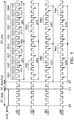
- FIG. 5 shows an exemplary waveform diagram of an alert handshake control line ALERT_HAND, for illustrating operations of the synchronization stage ST_Sync (the step S 312 ), the synchronization end stage ST_SyncEnd (the step S 314 ) and the assignment stage ST_Ass (step S 316 ) of the scheduling control method of FIG. 3 .
- FIGS. 5 shows an exemplary waveform diagram of an alert handshake control line ALERT_HAND, for illustrating operations of the synchronization stage ST_Sync (the step S 312 ), the synchronization end stage ST_SyncEnd (the step S 314 ) and the assignment stage ST_Ass (step S 316 ) of the scheduling control method of FIG. 3 . Please refer to FIGS.
- the slave device requesting an interrupt can control the alert handshake pin thereof to enter the output mode to output the low voltage level, so as to drive the alert handshake control line ALERT_HAND by clock cycles more than a specific number, such as more than three clock cycles, thereby facilitating other slave device of the bus system 1 to distinguish that the bus system 1 enters the synchronization stage ST_Sync rather than other phase such as assignment stage ST_Ass.
- the slave device requesting the interrupt can stop driving the alert handshake control line ALERT_HAND, and then control the alert handshake pin thereof to enter the input mode, so as to monitor the alert handshake control line ALERT_HAND.
- other slave devices of the bus system 1 can detect that the alert handshake control line ALERT_HAND is recovered as the high voltage level, so that all slave device can enter the synchronization end stage ST_SyncEnd, at the same time, in a step S 314 .
- each of the scheduling controllers 145 A to 145 D can wait at least one clock cycle, to ensure all of the slave devices 14 A to 14 D of the bus system 1 to complete the synchronization stage ST_Sync, and then the scheduling controllers 145 A to 145 D can control the slave devices 14 A to 14 D to enter the assignment stage ST_Ass from the synchronization end stage ST_SyncEnd, in a step S 316 .
- each of the plurality of slave devices 14 A to 14 D can monitor state of the alert handshake control line ALERT_HAND via the alert handshake pins Alert_ 1 to Alert _ 4 in each assignment period.
- each of the assignment periods AP 1 to AP 4 have 2 ⁇ 4 clock cycles CY 1 to CY 8 .
- each of assignment periods AP 1 to AP 4 can be divided into four phases PH 1 to PH 4 , and each phase comprises two clock cycles.
- the phase PH 1 comprises clock cycles CY 1 and CY 2
- the phases PH 2 comprises clock cycles CY 3 and CY 4
- the phase PH 3 comprises clock cycles CY 5 and CY 6
- the phase PH 4 comprises clock cycles CY 7 and CY 8 .
- each of slave devices 14 A to 14 D can execute the corresponding operation thereof according to the phases PH 1 to PH 4 .
- the slave device 14 A corresponds to the phase PH 1
- the slave device 14 B corresponds to the phase PH 2
- the slave device 14 C corresponds to the phase PH 3
- the slave device 14 D corresponds to the phase PH 4 .
- the corresponding relationship between the slave devices 14 A to 14 D and the phases PH 1 to PH 4 is determined by the address section selection pins 18 A to 18 D and the address entry selection pins 16 A to 16 D shown in FIG. 2 .
- the corresponding relationship between the slave devices 14 A to 14 D and the phases PH 1 to PH 4 can be determined by other hardware or software configurations.
- the slave devices 14 A to 14 D can count the clock cycles CY 1 to CY 8 of the assignment periods AP 1 to AP 4 according to rising edges of the clock signals clk 1 to clk 4 thereof.
- the slave device 14 A In the assignment stage ST_Ass, when the slave device 14 A communicates with the master device 10 , the slave device 14 A has right to drive the alert handshake control line ALERT_HAND in the phase PH 1 of the assignment period AP 1 only.
- the scheduling controller 145 A of the slave device 14 A can, in the phase PH 1 , control the alert handshake pin Alert_ 1 to enter the output mode, and output the low voltage level to drive the alert handshake control line ALERT_HAND, so as to control the alert handshake control line ALERT_HAND at the low voltage level.
- the scheduling controller 145 A of the slave device 14 A can, in the phase PH 1 , control the alert handshake pin Alert _ 1 to enter the input mode, and stop driving the alert handshake control line ALERT_HAND.
- the slave device 14 A can monitor the voltage level of the alert handshake control line ALERT_HAND, for determining whether the master device 10 is in communication with the slave devices 14 B to 14 D.
- the scheduling controller 145 A of the slave device 14 A can control the alert handshake pin Alert_ 1 to enter the input mode.
- the slave device 14 A can monitor, at the phase PH 2 as an arrowhead 412 shown in FIG.
- the voltage level of the alert handshake control line ALERT_HAND via the alert handshake pin Alert_ 1 so as to determine whether the slave device 14 B is in communication with the master device 10 . If the slave device 14 A detects that the alert handshake control line ALERT_HAND is at the high voltage level in the phase PH 2 , the scheduling controller 145 A determines that the slave device 14 B is not in communication with the plurality of master device 10 . If the slave device 14 A detects that the alert handshake control line ALERT_HAND is at the low voltage level in the phase PH 2 , the scheduling controller 145 A can determine that the slave device 14 B is communicating with the master device 10 .
- the slave device 14 A can monitor, at the phase PH 3 as an arrowhead 414 shown in FIG. 5 , the voltage level of the alert handshake control line ALERT_HAND via the alert handshake pin Alert_ 1 , so as to determine whether the slave device 14 C is in communication with the master device 10 . If the slave device 14 A detects that the alert handshake control line ALERT_HAND is at the high voltage level in the phase PH 3 , the scheduling controller 145 A can determine that the slave device 14 C is not in communication with the plurality of master device 10 .
- the scheduling controller 145 A can determine that the slave device 14 C is communicating with the master device 10 .
- each of slave devices 14 A to 14 D can determine which slave device is communicating with the master device 10 . Furthermore, by monitoring the rising edge in middle of each phase, such as the rising edge (marked by an arrowhead 416 ) or the falling edge (not shown in FIG. 5 ) between the clock cycles CY 7 and CY 8 , to prevent the time difference caused by a phase offset of the clock signals clk 1 to clk 4 .
- each of the slave devices 14 A to 14 D can monitor, via the alert handshake pins Alert_ 1 to Alert_ 4 in each assignment period AP, whether the alert handshake control line ALERT_HAND is driven. After the slave device driving the alert handshake control line ALERT_HAND completes the interrupt requirement thereof, the slave device stops driving the alert handshake control line ALERT_HAND.
- the scheduling controllers 145 A to 145 D can control the slave devices 14 A to 14 D to enter the idle wait stage ST_IdleWait again in a step S 308 .
- the scheduling controllers 145 A to 145 D can control the slave devices 14 A to 14 D to enter the idle wait stage ST_IdleWait again in a step S 308 .
- the scheduling controllers 145 A to 145 D can control the slave devices 14 A to 14 D to enter the idle wait stage ST_IdleWait again in a step S 308 .
- the slave devices 14 A to 14 D is permitted to drive the alert handshake control line ALERT_HAND.
- alert handshake control line ALERT_HAND when the alert handshake control line ALERT_HAND is driven by more than two clock cycles, it indicates that one of the slave devices is executing the synchronization stage ST_Sync, so the other slave devices return to the synchronization stage ST_Sync.
- FIG. 6 shows a waveform diagram of signal on the alert handshake control line ALERT_HAND, for illustrating an operation of the slave devices 14 A to 14 D driving the alert handshake control line ALERT_HAND according to the scheduling control method of FIG. 3 .
- the slave device 14 A in response to an interrupt requirement REQ 1 , requests to communicate with the master device 10 .
- the slave device 14 A can monitor the voltage level of the alert handshake control line ALERT_HAND first, to make sure that the alert handshake control line ALERT_HAND is not driven by the slave devices 14 B to 14 D.
- the slave device 14 A can control the alert handshake pin Alert_ 1 to enter the output mode and output the low-voltage-level signal within three clock cycles of the clock signal clk 1 , so as to drive the alert handshake control line ALERT_HAND for notifying the slave devices 14 B and 14 D to enter the synchronization stage ST_Sync. Since the bus system 1 is operating in the synchronization stage ST_Sync, even if the slave device 14 B generates an interrupt requirement REQ 2 , the slave device 14 B cannot drive the alert handshake control line ALERT_HAND.
- the slave device 14 A After completing the synchronization stage ST_Sync, the slave device 14 A can control the alert handshake pin Alert_ 1 to enter the input mode and stop driving the alert handshake control line ALERT_HAND. As a result, each of the plurality of slave devices 14 A to 14 D of the bus system 1 enter the synchronization end stage ST_SyncEnd. As mentioned previously, in the synchronization end stage ST_SyncEnd, the scheduling controllers 145 A to 145 D can wait at least one clock cycle, and then control the slave devices 14 A to 14 D to enter the assignment stage ST_Ass from the synchronization end stage ST_SyncEnd.
- the slave device 14 A can get the right to control the alert handshake control line ALERT_HAND, for communicating with the master device 10 .
- the alert handshake control line ALERT_HAND is changed to the low voltage level in the phase PH 1 of the assignment period AP 1 of the slave device 14 A. Therefore, the slave device 14 A can get the right to communicate with the master device 10 .
- the slave device 14 D can detect, in the phase PH 1 of the assignment period AP 4 , that the alert handshake control line ALERT_HAND is at the low voltage level. The slave device 14 D can detect that the slave device 14 A corresponding to the phase PH 1 is communicating with the master device 10 , for example, for processing the interrupt requirement.
- the slave device 14 B can detect, in the phase PH 1 of the assignment period AP 2 , that the alert handshake control line ALERT_HAND is at the low voltage level.
- the slave device 14 B can determine that the slave device 14 A corresponding to the phase PH 1 is communicating with the master device 10 .
- the slave device 14 C can detect, in the phase PH 1 of each assignment period AP 3 , that the alert handshake control line ALERT_HAND is at the low voltage level.
- the slave device 14 C can determine that the slave device 14 A corresponding to the phase PH 1 is processing the interrupt requirement.
- the slave device 14 A When the slave device 14 A is in communication with the master device 10 , the slave device 14 A can provide an event alert signal ALERT to the input/output signal line eSPI_IO of the bus 12 via the input/output signal line eSPI_IO 1 , so as to transmit the event alert signal ALERT to the master device 10 .
- the event alert signal ALERT can indicate the request signal of the slave device 14 A for communication with the master device 10 .
- one of slave devices 14 B to 14 D which wants to communicate with the master device 10 , can store the event message and then wait for getting the control right of the alert handshake control line ALERT_HAND to communicate with the master device 10 .
- the master device 10 transmits a status-retrieving signal GET_STATUS via the input/output signal line eSPI_IO, to query states of the slave devices 14 A to 14 D.
- the slave device 14 A receives the status-retrieving signal GET_STATUS via the input/output signal line eSPI_IO, and then respond to notice the master device 10 that there is information to be transmitted.
- the slave devices 14 B to 14 D do not receive and respond the status-retrieving signal GET_STATUS.
- the master device 10 transmits the event-retrieving signal GET_VWIRE via the input/output signal line eSPI_IO, for obtaining the event message of the slave device 14 A.
- the slave device 14 A receives and responds the event-retrieving signal GET_VWIRE, to transmit the event message to the master device 10 .
- the slave devices 14 B to 14 D does not receive and respond the event-retrieving signal GET_VWIRE.
- the slave device 14 A When the slave device 14 A communicates with the master device 10 , the slave device 14 A can drive the alert handshake control line ALERT_HAND in the phase PH 1 of each assignment period AP 1 until the slave device 14 A ends the communication with the master device 10 .
- the slave device 14 D can detect, in the phase PH 1 of the assignment period AP 4 , that the alert handshake control line ALERT_HAND is changed to the high voltage level.
- the slave device 14 D can determine that the slave device 14 A corresponding to the phase PH 1 ends the communication with the master device 10 .
- the slave device 14 B and 14 C can detect, in the phases PH 1 of the assignment periods AP 2 and AP 3 respectively, that the alert handshake control line ALERT_HAND is changed to the high voltage level.
- the slave device 14 B and 14 C can determine that the slave device 14 A corresponding to the phase PH 1 ends the communication with the master device 10 .
- the scheduling controllers 145 B to 145 D can control the slave devices 14 B to 14 D to enter the idle wait stage ST_IdleWait.
- the slave device 14 A ends the communication with the master device 10 , the slave device 14 A does not drive the alert handshake control line ALERT_HAND in the phase PH 1 of the assignment period AP 1 , so that the slave devices 14 A to 14 D can enter the idle wait stage ST_IdleWait after the phase PH 1 .
- the scheduling controllers 145 A to 145 D of the slave devices 14 A to 14 D can control the corresponding alert handshake pins Alert_ 1 to Alert_ 4 to enter the input mode, so as to monitor whether the alert handshake control line ALERT_HAND is driven by any one of the slave devices 14 A to 14 D.
- the slave device 14 B can control the alert handshake pin Alert_ 2 to enter the output mode and output the low voltage level within three clock cycles of the clock signal clk 2 , to drive the alert handshake control line ALERT_HAND, to notice the slave devices 14 A, 14 C and 14 D to enter the synchronization stage ST_Sync.
- the bus system 1 enters the synchronization end stage ST_SyncEnd and the assignment stage ST_Ass, in a sequential order.
- the slave device 14 B can control the alert handshake pin Alert_ 2 , in the phase PH 2 corresponding to the slave device 14 B, to enter the output mode and output the low voltage level, so as to drive the alert handshake control line ALERT_HAND, and perform further communication.
- an accumulated offset (such as frequency or phase) between the clock signals of the slave devices may easily cause scheduling error or collision.
- the scheduling controller can control all slave devices to enter the synchronization stage ST_Sync again, so as to prevent the bus system from continuously operating in the assignment stage ST_Ass, thereby resetting the offset between the clock signals of all slave devices to zero.
- the slave devices do not count different time periods, so as to prevent the scheduling error or collision.
- the scheduling controller can monitor, in each assignment period, the voltage levels of the alert handshake control line ALERT_HAND in other phases other than the phase thereof, so that the scheduling controller can determine which slave device is currently communicating with the master device.
- the bus system can allow the user to identify or a developer to debug more quickly.
- the interrupt requirements of different slave devices can occur at different time points, so as to prevent the slave devices from snatching the alert handshake control line ALERT_HAND to cause the master device to communicate with incorrect slave device.
- the pin (such as the address section selection pin and the address entry selection pin) of the slave device can be used to set the corresponding phase without adding more pins.
Landscapes
- Engineering & Computer Science (AREA)
- Theoretical Computer Science (AREA)
- General Engineering & Computer Science (AREA)
- Physics & Mathematics (AREA)
- General Physics & Mathematics (AREA)
- Computer Hardware Design (AREA)
- Information Transfer Systems (AREA)
- Debugging And Monitoring (AREA)
Abstract
Description
Claims (10)
Applications Claiming Priority (2)
| Application Number | Priority Date | Filing Date | Title |
|---|---|---|---|
| TW107144994A TWI706257B (en) | 2018-12-13 | 2018-12-13 | Bus system |
| TW107144994 | 2018-12-13 |
Publications (2)
| Publication Number | Publication Date |
|---|---|
| US20200192449A1 US20200192449A1 (en) | 2020-06-18 |
| US11216049B2 true US11216049B2 (en) | 2022-01-04 |
Family
ID=71071532
Family Applications (1)
| Application Number | Title | Priority Date | Filing Date |
|---|---|---|---|
| US16/713,745 Active 2040-01-01 US11216049B2 (en) | 2018-12-13 | 2019-12-13 | Bus system |
Country Status (2)
| Country | Link |
|---|---|
| US (1) | US11216049B2 (en) |
| TW (1) | TWI706257B (en) |
Cited By (1)
| Publication number | Priority date | Publication date | Assignee | Title |
|---|---|---|---|---|
| US11609877B1 (en) * | 2021-09-24 | 2023-03-21 | Qualcomm Incorporated | Systems and methods for chip operation using serial peripheral interface (SPI) without a chip select pin |
Families Citing this family (5)
| Publication number | Priority date | Publication date | Assignee | Title |
|---|---|---|---|---|
| TWI773247B (en) * | 2021-04-13 | 2022-08-01 | 新唐科技股份有限公司 | Bus system |
| TWI775436B (en) | 2021-05-17 | 2022-08-21 | 新唐科技股份有限公司 | Bus system |
| TWI791271B (en) | 2021-08-25 | 2023-02-01 | 新唐科技股份有限公司 | Bus system |
| TWI813104B (en) * | 2021-12-23 | 2023-08-21 | 新唐科技股份有限公司 | Bus system |
| TWI836871B (en) * | 2023-01-18 | 2024-03-21 | 新唐科技股份有限公司 | Bus system |
Citations (10)
| Publication number | Priority date | Publication date | Assignee | Title |
|---|---|---|---|---|
| US5081701A (en) * | 1987-04-20 | 1992-01-14 | Tandem Computers Incorporated | System for controlling data transfer using transfer handshake protocol using transfer complete and transfer inhibit signals |
| US5765217A (en) * | 1995-03-01 | 1998-06-09 | Motorola, Inc. | Method and apparatus to perform bus reflection operation using a data processor |
| US6807593B1 (en) * | 2001-11-01 | 2004-10-19 | Lsi Logic Corporation | Enhanced bus architecture for posted read operation between masters and slaves |
| US20100153602A1 (en) * | 2008-12-12 | 2010-06-17 | Fujitsu Microelectronics Limited | Computer system and abnormality detection circuit |
| US20110106991A1 (en) * | 2009-10-29 | 2011-05-05 | Renesas Electronics Corporation | Bus system and bus control method |
| US8190803B2 (en) * | 2002-02-19 | 2012-05-29 | Schism Electronics, L.L.C. | Hierarchical bus structure and memory access protocol for multiprocessor systems |
| US20130322462A1 (en) * | 2012-06-01 | 2013-12-05 | Research In Motion Limited | Universal synchronization engine based on probabilistic methods for guarantee of lock in multiformat audio systems |
| US20140112339A1 (en) * | 2012-10-22 | 2014-04-24 | Robert J. Safranek | High performance interconnect |
| US20170153997A1 (en) * | 2015-11-26 | 2017-06-01 | Nuvoton Technology Corporation | Bus system |
| TWI671638B (en) | 2018-05-24 | 2019-09-11 | 新唐科技股份有限公司 | Bus system |
-
2018
- 2018-12-13 TW TW107144994A patent/TWI706257B/en active
-
2019
- 2019-12-13 US US16/713,745 patent/US11216049B2/en active Active
Patent Citations (14)
| Publication number | Priority date | Publication date | Assignee | Title |
|---|---|---|---|---|
| US5081701A (en) * | 1987-04-20 | 1992-01-14 | Tandem Computers Incorporated | System for controlling data transfer using transfer handshake protocol using transfer complete and transfer inhibit signals |
| US5765217A (en) * | 1995-03-01 | 1998-06-09 | Motorola, Inc. | Method and apparatus to perform bus reflection operation using a data processor |
| US6807593B1 (en) * | 2001-11-01 | 2004-10-19 | Lsi Logic Corporation | Enhanced bus architecture for posted read operation between masters and slaves |
| US8190803B2 (en) * | 2002-02-19 | 2012-05-29 | Schism Electronics, L.L.C. | Hierarchical bus structure and memory access protocol for multiprocessor systems |
| US20100153602A1 (en) * | 2008-12-12 | 2010-06-17 | Fujitsu Microelectronics Limited | Computer system and abnormality detection circuit |
| US20110106991A1 (en) * | 2009-10-29 | 2011-05-05 | Renesas Electronics Corporation | Bus system and bus control method |
| US20130322462A1 (en) * | 2012-06-01 | 2013-12-05 | Research In Motion Limited | Universal synchronization engine based on probabilistic methods for guarantee of lock in multiformat audio systems |
| CN104541473A (en) | 2012-06-01 | 2015-04-22 | 黑莓有限公司 | A general-purpose synchronization engine for guaranteed lock in multi-format audio systems based on probabilistic methods |
| CN104541473B (en) | 2012-06-01 | 2017-09-12 | 黑莓有限公司 | Being used for based on probabilistic method ensures the generic sync engine of the locking in multi-format audio system |
| US20140112339A1 (en) * | 2012-10-22 | 2014-04-24 | Robert J. Safranek | High performance interconnect |
| CN104969206A (en) | 2012-10-22 | 2015-10-07 | 英特尔公司 | High performance interconnect physical layer |
| CN104969206B (en) | 2012-10-22 | 2017-12-26 | 英特尔公司 | High Performance Interconnect Physical Layer |
| US20170153997A1 (en) * | 2015-11-26 | 2017-06-01 | Nuvoton Technology Corporation | Bus system |
| TWI671638B (en) | 2018-05-24 | 2019-09-11 | 新唐科技股份有限公司 | Bus system |
Non-Patent Citations (1)
| Title |
|---|
| Office Action dated Jan. 17, 2020 in corresponding TW Application No. 107144994. |
Cited By (2)
| Publication number | Priority date | Publication date | Assignee | Title |
|---|---|---|---|---|
| US11609877B1 (en) * | 2021-09-24 | 2023-03-21 | Qualcomm Incorporated | Systems and methods for chip operation using serial peripheral interface (SPI) without a chip select pin |
| US20230095850A1 (en) * | 2021-09-24 | 2023-03-30 | Qualcomm Incorporated | Systems and methods for chip operation using serial peripheral interface (spi) without a chip select pin |
Also Published As
| Publication number | Publication date |
|---|---|
| US20200192449A1 (en) | 2020-06-18 |
| TWI706257B (en) | 2020-10-01 |
| TW202022628A (en) | 2020-06-16 |
Similar Documents
| Publication | Publication Date | Title |
|---|---|---|
| US11216049B2 (en) | Bus system | |
| US10936524B2 (en) | Bus system with slave devices | |
| US7788431B2 (en) | Dynamic I2C slave device address decoder | |
| US7979597B2 (en) | Programming parallel I2C slave devices from a single I2C data stream | |
| US6145036A (en) | Polling of failed devices on an I2 C bus | |
| US10657088B2 (en) | Integrated circuit, bus system and control method thereof | |
| US5758099A (en) | Plug and play protocol for bus adapter card | |
| EP4198756A1 (en) | Daisy-chain spi integrated circuit and operation method thereof | |
| US7562172B2 (en) | I2C Slave/master interface enhancement using state machines | |
| US10817452B2 (en) | Bus system and detection method thereof | |
| US11321258B2 (en) | Integrated circuit, bus system and scheduling method | |
| CN105468548A (en) | Serial peripheral interface | |
| US11907155B2 (en) | Bus system connecting slave devices with single-wire data access communication | |
| US7761637B2 (en) | Slave device with latched request for service | |
| US10901935B2 (en) | IC, bus system and control method thereof | |
| CN100426274C (en) | Method and device for preventing I2C bus locked | |
| EP3182295A1 (en) | Communication system with serial ports for automatically identifying device types and communication protocols and method thereof | |
| US12093207B2 (en) | Serial peripheral interface with multi-controller daisy chain | |
| US20230205725A1 (en) | Bus system | |
| WO2024112352A1 (en) | Flexible bus communication | |
| US20050172036A1 (en) | Method for transmitting data in a multi-chip system | |
| CN118363908A (en) | Bus system | |
| TW201421246A (en) | Method for transiting signals, system of transferring signals and expansion card |
Legal Events
| Date | Code | Title | Description |
|---|---|---|---|
| FEPP | Fee payment procedure |
Free format text: ENTITY STATUS SET TO UNDISCOUNTED (ORIGINAL EVENT CODE: BIG.); ENTITY STATUS OF PATENT OWNER: LARGE ENTITY |
|
| AS | Assignment |
Owner name: NUVOTON TECHNOLOGY CORPORATION, TAIWAN Free format text: ASSIGNMENT OF ASSIGNORS INTEREST;ASSIGNORS:HUANG, CHIH-HUNG;CHIU, CHUN-WEI;CHANG, HAO-YANG;REEL/FRAME:051345/0862 Effective date: 20191210 |
|
| STPP | Information on status: patent application and granting procedure in general |
Free format text: APPLICATION DISPATCHED FROM PREEXAM, NOT YET DOCKETED |
|
| STPP | Information on status: patent application and granting procedure in general |
Free format text: NON FINAL ACTION MAILED |
|
| STPP | Information on status: patent application and granting procedure in general |
Free format text: RESPONSE TO NON-FINAL OFFICE ACTION ENTERED AND FORWARDED TO EXAMINER |
|
| STPP | Information on status: patent application and granting procedure in general |
Free format text: FINAL REJECTION MAILED |
|
| STPP | Information on status: patent application and granting procedure in general |
Free format text: NOTICE OF ALLOWANCE MAILED -- APPLICATION RECEIVED IN OFFICE OF PUBLICATIONS |
|
| STPP | Information on status: patent application and granting procedure in general |
Free format text: PUBLICATIONS -- ISSUE FEE PAYMENT RECEIVED |
|
| STPP | Information on status: patent application and granting procedure in general |
Free format text: PUBLICATIONS -- ISSUE FEE PAYMENT VERIFIED |
|
| STCF | Information on status: patent grant |
Free format text: PATENTED CASE |
|
| MAFP | Maintenance fee payment |
Free format text: PAYMENT OF MAINTENANCE FEE, 4TH YEAR, LARGE ENTITY (ORIGINAL EVENT CODE: M1551); ENTITY STATUS OF PATENT OWNER: LARGE ENTITY Year of fee payment: 4 |