US11215892B2 - Display device - Google Patents
Display device Download PDFInfo
- Publication number
- US11215892B2 US11215892B2 US16/885,272 US202016885272A US11215892B2 US 11215892 B2 US11215892 B2 US 11215892B2 US 202016885272 A US202016885272 A US 202016885272A US 11215892 B2 US11215892 B2 US 11215892B2
- Authority
- US
- United States
- Prior art keywords
- display device
- extending
- signal line
- pixel electrode
- disposed
- Prior art date
- Legal status (The legal status is an assumption and is not a legal conclusion. Google has not performed a legal analysis and makes no representation as to the accuracy of the status listed.)
- Active
Links
Images


Classifications
-
- G—PHYSICS
- G02—OPTICS
- G02F—OPTICAL DEVICES OR ARRANGEMENTS FOR THE CONTROL OF LIGHT BY MODIFICATION OF THE OPTICAL PROPERTIES OF THE MEDIA OF THE ELEMENTS INVOLVED THEREIN; NON-LINEAR OPTICS; FREQUENCY-CHANGING OF LIGHT; OPTICAL LOGIC ELEMENTS; OPTICAL ANALOGUE/DIGITAL CONVERTERS
- G02F1/00—Devices or arrangements for the control of the intensity, colour, phase, polarisation or direction of light arriving from an independent light source, e.g. switching, gating or modulating; Non-linear optics
- G02F1/01—Devices or arrangements for the control of the intensity, colour, phase, polarisation or direction of light arriving from an independent light source, e.g. switching, gating or modulating; Non-linear optics for the control of the intensity, phase, polarisation or colour
- G02F1/13—Devices or arrangements for the control of the intensity, colour, phase, polarisation or direction of light arriving from an independent light source, e.g. switching, gating or modulating; Non-linear optics for the control of the intensity, phase, polarisation or colour based on liquid crystals, e.g. single liquid crystal display cells
- G02F1/133—Constructional arrangements; Operation of liquid crystal cells; Circuit arrangements
- G02F1/1333—Constructional arrangements; Manufacturing methods
- G02F1/1343—Electrodes
- G02F1/134309—Electrodes characterised by their geometrical arrangement
-
- G—PHYSICS
- G02—OPTICS
- G02F—OPTICAL DEVICES OR ARRANGEMENTS FOR THE CONTROL OF LIGHT BY MODIFICATION OF THE OPTICAL PROPERTIES OF THE MEDIA OF THE ELEMENTS INVOLVED THEREIN; NON-LINEAR OPTICS; FREQUENCY-CHANGING OF LIGHT; OPTICAL LOGIC ELEMENTS; OPTICAL ANALOGUE/DIGITAL CONVERTERS
- G02F1/00—Devices or arrangements for the control of the intensity, colour, phase, polarisation or direction of light arriving from an independent light source, e.g. switching, gating or modulating; Non-linear optics
- G02F1/01—Devices or arrangements for the control of the intensity, colour, phase, polarisation or direction of light arriving from an independent light source, e.g. switching, gating or modulating; Non-linear optics for the control of the intensity, phase, polarisation or colour
- G02F1/13—Devices or arrangements for the control of the intensity, colour, phase, polarisation or direction of light arriving from an independent light source, e.g. switching, gating or modulating; Non-linear optics for the control of the intensity, phase, polarisation or colour based on liquid crystals, e.g. single liquid crystal display cells
- G02F1/133—Constructional arrangements; Operation of liquid crystal cells; Circuit arrangements
- G02F1/1333—Constructional arrangements; Manufacturing methods
- G02F1/1343—Electrodes
-
- G—PHYSICS
- G02—OPTICS
- G02F—OPTICAL DEVICES OR ARRANGEMENTS FOR THE CONTROL OF LIGHT BY MODIFICATION OF THE OPTICAL PROPERTIES OF THE MEDIA OF THE ELEMENTS INVOLVED THEREIN; NON-LINEAR OPTICS; FREQUENCY-CHANGING OF LIGHT; OPTICAL LOGIC ELEMENTS; OPTICAL ANALOGUE/DIGITAL CONVERTERS
- G02F1/00—Devices or arrangements for the control of the intensity, colour, phase, polarisation or direction of light arriving from an independent light source, e.g. switching, gating or modulating; Non-linear optics
- G02F1/01—Devices or arrangements for the control of the intensity, colour, phase, polarisation or direction of light arriving from an independent light source, e.g. switching, gating or modulating; Non-linear optics for the control of the intensity, phase, polarisation or colour
- G02F1/13—Devices or arrangements for the control of the intensity, colour, phase, polarisation or direction of light arriving from an independent light source, e.g. switching, gating or modulating; Non-linear optics for the control of the intensity, phase, polarisation or colour based on liquid crystals, e.g. single liquid crystal display cells
- G02F1/133—Constructional arrangements; Operation of liquid crystal cells; Circuit arrangements
- G02F1/136—Liquid crystal cells structurally associated with a semi-conducting layer or substrate, e.g. cells forming part of an integrated circuit
- G02F1/1362—Active matrix addressed cells
- G02F1/136286—Wiring, e.g. gate line, drain line
-
- G—PHYSICS
- G02—OPTICS
- G02F—OPTICAL DEVICES OR ARRANGEMENTS FOR THE CONTROL OF LIGHT BY MODIFICATION OF THE OPTICAL PROPERTIES OF THE MEDIA OF THE ELEMENTS INVOLVED THEREIN; NON-LINEAR OPTICS; FREQUENCY-CHANGING OF LIGHT; OPTICAL LOGIC ELEMENTS; OPTICAL ANALOGUE/DIGITAL CONVERTERS
- G02F1/00—Devices or arrangements for the control of the intensity, colour, phase, polarisation or direction of light arriving from an independent light source, e.g. switching, gating or modulating; Non-linear optics
- G02F1/01—Devices or arrangements for the control of the intensity, colour, phase, polarisation or direction of light arriving from an independent light source, e.g. switching, gating or modulating; Non-linear optics for the control of the intensity, phase, polarisation or colour
- G02F1/13—Devices or arrangements for the control of the intensity, colour, phase, polarisation or direction of light arriving from an independent light source, e.g. switching, gating or modulating; Non-linear optics for the control of the intensity, phase, polarisation or colour based on liquid crystals, e.g. single liquid crystal display cells
- G02F1/133—Constructional arrangements; Operation of liquid crystal cells; Circuit arrangements
- G02F1/1333—Constructional arrangements; Manufacturing methods
- G02F1/1335—Structural association of cells with optical devices, e.g. polarisers or reflectors
- G02F1/133509—Filters, e.g. light shielding masks
- G02F1/133512—Light shielding layers, e.g. black matrix
-
- G—PHYSICS
- G02—OPTICS
- G02F—OPTICAL DEVICES OR ARRANGEMENTS FOR THE CONTROL OF LIGHT BY MODIFICATION OF THE OPTICAL PROPERTIES OF THE MEDIA OF THE ELEMENTS INVOLVED THEREIN; NON-LINEAR OPTICS; FREQUENCY-CHANGING OF LIGHT; OPTICAL LOGIC ELEMENTS; OPTICAL ANALOGUE/DIGITAL CONVERTERS
- G02F1/00—Devices or arrangements for the control of the intensity, colour, phase, polarisation or direction of light arriving from an independent light source, e.g. switching, gating or modulating; Non-linear optics
- G02F1/01—Devices or arrangements for the control of the intensity, colour, phase, polarisation or direction of light arriving from an independent light source, e.g. switching, gating or modulating; Non-linear optics for the control of the intensity, phase, polarisation or colour
- G02F1/13—Devices or arrangements for the control of the intensity, colour, phase, polarisation or direction of light arriving from an independent light source, e.g. switching, gating or modulating; Non-linear optics for the control of the intensity, phase, polarisation or colour based on liquid crystals, e.g. single liquid crystal display cells
- G02F1/133—Constructional arrangements; Operation of liquid crystal cells; Circuit arrangements
- G02F1/1333—Constructional arrangements; Manufacturing methods
- G02F1/1337—Surface-induced orientation of the liquid crystal molecules, e.g. by alignment layers
- G02F1/133707—Structures for producing distorted electric fields, e.g. bumps, protrusions, recesses, slits in pixel electrodes
-
- G—PHYSICS
- G02—OPTICS
- G02F—OPTICAL DEVICES OR ARRANGEMENTS FOR THE CONTROL OF LIGHT BY MODIFICATION OF THE OPTICAL PROPERTIES OF THE MEDIA OF THE ELEMENTS INVOLVED THEREIN; NON-LINEAR OPTICS; FREQUENCY-CHANGING OF LIGHT; OPTICAL LOGIC ELEMENTS; OPTICAL ANALOGUE/DIGITAL CONVERTERS
- G02F1/00—Devices or arrangements for the control of the intensity, colour, phase, polarisation or direction of light arriving from an independent light source, e.g. switching, gating or modulating; Non-linear optics
- G02F1/01—Devices or arrangements for the control of the intensity, colour, phase, polarisation or direction of light arriving from an independent light source, e.g. switching, gating or modulating; Non-linear optics for the control of the intensity, phase, polarisation or colour
- G02F1/13—Devices or arrangements for the control of the intensity, colour, phase, polarisation or direction of light arriving from an independent light source, e.g. switching, gating or modulating; Non-linear optics for the control of the intensity, phase, polarisation or colour based on liquid crystals, e.g. single liquid crystal display cells
- G02F1/133—Constructional arrangements; Operation of liquid crystal cells; Circuit arrangements
- G02F1/1333—Constructional arrangements; Manufacturing methods
- G02F1/1343—Electrodes
- G02F1/134309—Electrodes characterised by their geometrical arrangement
- G02F1/134345—Subdivided pixels, e.g. for grey scale or redundancy
-
- G—PHYSICS
- G02—OPTICS
- G02F—OPTICAL DEVICES OR ARRANGEMENTS FOR THE CONTROL OF LIGHT BY MODIFICATION OF THE OPTICAL PROPERTIES OF THE MEDIA OF THE ELEMENTS INVOLVED THEREIN; NON-LINEAR OPTICS; FREQUENCY-CHANGING OF LIGHT; OPTICAL LOGIC ELEMENTS; OPTICAL ANALOGUE/DIGITAL CONVERTERS
- G02F1/00—Devices or arrangements for the control of the intensity, colour, phase, polarisation or direction of light arriving from an independent light source, e.g. switching, gating or modulating; Non-linear optics
- G02F1/01—Devices or arrangements for the control of the intensity, colour, phase, polarisation or direction of light arriving from an independent light source, e.g. switching, gating or modulating; Non-linear optics for the control of the intensity, phase, polarisation or colour
- G02F1/13—Devices or arrangements for the control of the intensity, colour, phase, polarisation or direction of light arriving from an independent light source, e.g. switching, gating or modulating; Non-linear optics for the control of the intensity, phase, polarisation or colour based on liquid crystals, e.g. single liquid crystal display cells
- G02F1/133—Constructional arrangements; Operation of liquid crystal cells; Circuit arrangements
- G02F1/136—Liquid crystal cells structurally associated with a semi-conducting layer or substrate, e.g. cells forming part of an integrated circuit
- G02F1/1362—Active matrix addressed cells
- G02F1/1368—Active matrix addressed cells in which the switching element is a three-electrode device
-
- G—PHYSICS
- G02—OPTICS
- G02F—OPTICAL DEVICES OR ARRANGEMENTS FOR THE CONTROL OF LIGHT BY MODIFICATION OF THE OPTICAL PROPERTIES OF THE MEDIA OF THE ELEMENTS INVOLVED THEREIN; NON-LINEAR OPTICS; FREQUENCY-CHANGING OF LIGHT; OPTICAL LOGIC ELEMENTS; OPTICAL ANALOGUE/DIGITAL CONVERTERS
- G02F2201/00—Constructional arrangements not provided for in groups G02F1/00 - G02F7/00
- G02F2201/12—Constructional arrangements not provided for in groups G02F1/00 - G02F7/00 electrode
- G02F2201/121—Constructional arrangements not provided for in groups G02F1/00 - G02F7/00 electrode common or background
-
- G—PHYSICS
- G02—OPTICS
- G02F—OPTICAL DEVICES OR ARRANGEMENTS FOR THE CONTROL OF LIGHT BY MODIFICATION OF THE OPTICAL PROPERTIES OF THE MEDIA OF THE ELEMENTS INVOLVED THEREIN; NON-LINEAR OPTICS; FREQUENCY-CHANGING OF LIGHT; OPTICAL LOGIC ELEMENTS; OPTICAL ANALOGUE/DIGITAL CONVERTERS
- G02F2201/00—Constructional arrangements not provided for in groups G02F1/00 - G02F7/00
- G02F2201/12—Constructional arrangements not provided for in groups G02F1/00 - G02F7/00 electrode
- G02F2201/122—Constructional arrangements not provided for in groups G02F1/00 - G02F7/00 electrode having a particular pattern
-
- G—PHYSICS
- G02—OPTICS
- G02F—OPTICAL DEVICES OR ARRANGEMENTS FOR THE CONTROL OF LIGHT BY MODIFICATION OF THE OPTICAL PROPERTIES OF THE MEDIA OF THE ELEMENTS INVOLVED THEREIN; NON-LINEAR OPTICS; FREQUENCY-CHANGING OF LIGHT; OPTICAL LOGIC ELEMENTS; OPTICAL ANALOGUE/DIGITAL CONVERTERS
- G02F2201/00—Constructional arrangements not provided for in groups G02F1/00 - G02F7/00
- G02F2201/12—Constructional arrangements not provided for in groups G02F1/00 - G02F7/00 electrode
- G02F2201/123—Constructional arrangements not provided for in groups G02F1/00 - G02F7/00 electrode pixel
Definitions
- the present disclosure relates to a display device.
- a display device includes a display panel including a plurality of pixels capable of displaying an image.
- Each pixel may include a pixel electrode receiving a data signal, and the pixel electrode is connected to at least one transistor to receive a data voltage.
- a liquid crystal display includes field generating electrodes including the pixel electrode and a common electrode, and a liquid crystal layer interposed therebetween.
- the liquid crystal display applies a voltage to the field generating electrodes to generate an electric field to the liquid crystal layer, such that a direction of liquid crystal molecules in the liquid crystal layer is altered and a desired image may be displayed by controlling polarization of incident light.
- a signal line may be disposed in a transmissive region of each pixel as the size of the pixel becomes smaller and the transmissive region of each pixel becomes smaller.
- dispersion occurs in the width, position, or the like of the signal line in the process of forming the signal line, it also affects the dispersion of the transmittance of the pixel.
- the present disclosure is intended to minimize the dispersion of the transmittance of the pixel in the display device in which the signal line is disposed in the transmissive region of the pixel.
- a display device includes: a signal line extending in a direction perpendicular to a first direction; a transistor electrically connected to the signal line; and a pixel electrode electrically connected to the transistor and including a branch electrode, wherein the branch electrode incudes a first portion and a second portion extending from the first portion and extending in a direction different from an extending direction of the first portion, an acute angle formed between an extending direction of the second portion and the first direction is smaller than an acute angle formed between the extending direction of the first portion and the first direction, and the signal line overlaps the second portion in a plan view.
- each pixel may include a transmissive region through which light is capable of being transmitted and a light blocking region through which light is not capable of being transmitted, the transistor may be disposed in the light blocking region, and the signal line may extend in the direction perpendicular to the first direction at the transmissive region.
- Two parallel edges of the signal line may overlap the second portion.
- a width of the second portion in the first direction may be greater than or equal to a width of the signal line in the first direction.
- the signal line may be a data line transmitting a data voltage to the transistor.
- the branch electrode may further include a third portion extending from the second portion, the second portion may be disposed between the first portion and the third portion, and an acute angle formed between the extending direction of the second portion and the first direction may be smaller than an acute angle formed between an extending direction of the third portion and the first direction.
- the extending direction of the first portion and the extending direction of the third portion may be the same.
- a width of the first portion and a width of the third portion may be constant.
- the pixel electrode may further include: a transverse stem extending in a different direction from the extending direction of the first portion; and a longitudinal stem extending in a direction perpendicular to the extending direction of the transverse stem, and intersecting the transverse stem, and the branch electrode may extend obliquely from the transverse stem or the longitudinal stem.
- the display device may further include a common electrode opposing the pixel electrode and a liquid crystal layer including liquid crystal molecules and interposed between the pixel electrode and the common electrode.
- a display device includes a pixel including: a transmissive region and a light blocking region; a signal line extending in a first direction in the transmissive region; a pixel electrode disposed at the transmissive region; and a transistor disposed at the light blocking region, wherein the pixel electrode includes a branch electrode including a first portion and a second portion extending in directions different from each other, the first portion extends in a direction different from the first direction and a second direction which extends perpendicular to the first direction, and the signal line overlaps the second portion in a plan view.
- a display device includes: a substrate; a signal line and a transistor disposed on the substrate; and a pixel electrode disposed on the transistor and the signal line, wherein the pixel electrode includes a branch electrode including a first portion and a second portion extending in different directions from each other in a plan view, an acute angle formed between a direction perpendicular to an extending direction of the signal line and an extending direction of the second portion is smaller than an acute angle formed between the direction perpendicular to the extending direction of the signal line and the extending direction of the first portion in a plan view, and the signal line overlaps the second portion in a plan view.
- the dispersion of the transmittance of the pixel may be minimized.
- FIG. 1 is a schematic layout view of a display device according to an exemplary embodiment of the present inventive concept
- FIG. 2 is a layout view of one pixel of a display device according to an exemplary embodiment of the present inventive concept
- FIG. 3 is a cross-sectional view of a display device shown in FIG. 2 taken along a line IIIa-IIIb,
- FIG. 4 is a cross-sectional view of a display device shown in FIG. 2 taken along a line IVa-IVb,
- FIG. 5 is a top plan view showing a part of one pixel of a display device according to an exemplary embodiment of the present inventive concept
- FIG. 6 is a top plan view showing a part of a pixel electrode of a display device according to an exemplary embodiment of the present inventive concept
- FIG. 7 is a cross-sectional view of a display device shown in FIG. 5 taken along a line VIIa-VIIb,
- FIG. 8 is a top plan view showing a part of one pixel of a display device according to a comparative example
- FIG. 9 is a cross-sectional view of a display device shown in FIG. 8 taken along a line IXa-IXb,
- FIG. 10 is a top plan view showing a part of one pixel of a display device according to an exemplary embodiment of the present inventive concept
- FIG. 11 is a graph illustrating a change rate of transmittance of a pixel according to a change in a misalignment of a signal line in a display device according to a comparative example and an exemplary embodiment of the present inventive concept,
- FIG. 12 is a graph showing a change rate of transmittance of a pixel according to a width change of a signal line in a display device according to a comparative example and an exemplary embodiment of the present inventive concept,
- FIG. 13 , FIG. 14 and FIG. 15 are top plan views of a pixel electrode of a display device according to an exemplary embodiment of the present inventive concept, respectively,
- FIG. 16 is a top plan view showing a part of one pixel of a display device according to an exemplary embodiment of the present inventive concept
- FIG. 17 is a variation of a cross-sectional view of a display device shown in FIG. 2 taken along a line IIIa-IIIb,
- FIG. 18 is a layout view of one pixel of a display device according to an exemplary embodiment of the present inventive concept
- FIG. 19 a cross-sectional view of a display device shown in FIG. 18 taken along a line XIXa-XIXb, and
- FIG. 20 is a cross-sectional view of a display device shown in FIG. 18 taken along a line XXa-XXb.
- a plan view means a view when observing a surface parallel to two directions (e.g., a first direction DR 1 and a second direction DR 2 ) crossing each other
- a cross-sectional view means a view when observing a surface cut in a direction (e.g., a third direction DR 3 ) perpendicular to the surface parallel to the first direction DR 1 and the second direction DR 2
- to overlap two constituent elements means that two constituent elements are overlapped in the third direction DR 3 (e.g., a direction perpendicular to an upper surface of the substrate) unless stated otherwise.
- FIG. 1 a display device according to an exemplary embodiment of the present inventive concept is described with reference to FIG. 1 .
- FIG. 1 is a schematic layout view of a display device according to an exemplary embodiment of the present inventive concept
- a display device 1000 includes a display panel 300 including a display area DA and a peripheral area PA disposed outside the display area DA to surround the display area DA.
- the display panel 300 includes a first substrate 110 .
- the display area DA is an area which is capable of displaying an image according to an input image signal, and includes a plurality of pixels PX, a plurality of gate lines 121 , and a plurality of data lines 171 .
- the pixel PX is a basic unit for displaying an image, and each pixel PX may include at least one transistor and at least one pixel electrode electrically connected to the transistor. Each pixel PX may have a transmissive region through which light may be transmitted, and a light blocking region through which light may be relatively low or light may not be transmitted.
- the plurality of pixels PX may be regularly arranged, for example, in a matrix form.
- each pixel PX may display one of primary colors, and an image of a desired color may be recognized by a spatial and temporal sum of these primary colors.
- the primary colors may include, for example, three primary colors such as red, green, and blue, and may further include white.
- the gate line 121 may transfer a gate signal including a gate-on voltage and a gate-off voltage.
- the plurality of gate lines 121 may be generally arranged in parallel with each other in the second direction DR 2 , and each of the gate lines 121 may extend in the first direction DR 1 .
- the data line 171 may transmit a data voltage corresponding to the input image signal.
- the plurality of data lines 171 may be generally arranged in a direction parallel to the first direction DR 1 , and each of the data lines 171 may generally extend in the second direction DR 2 .
- the plurality of pixels PX disposed in one pixel column extending in the second direction DR 2 may be alternately electrically connected to two adjacent data lines 171 .
- the plurality of pixels PX of each pixel column may be alternately connected to two data lines 171 on a basis of one pixel row (or periodically).
- the plurality of pixels PX of each pixel column may be alternately connected to two adjacent data lines 171 on a basis of two or more pixel rows.
- the peripheral area PA may be an area that mostly does not display the image and is an area adjacent to the display area DA.
- the peripheral area PA may surround the display area DA.
- at least a portion of the peripheral area PA may display the image.
- the peripheral area PA may include gate drivers 400 a and 400 b.
- the gate drivers 400 a and 400 b may be electrically connected to the plurality of gate lines 121 to apply a gate signal.
- FIG. 1 illustrates an example in which the first gate driver 400 a is disposed in the peripheral area PA disposed on the left side of the display area DA, and the second gate driver 400 a is disposed in the peripheral area PA disposed on the right side of the display area DA.
- the gate drivers 400 a and 400 b may generate the gate signal including the gate-on voltage and the gate-off voltage, and may sequentially apply the gate signal to the plurality of gate lines 121 in a direction parallel to the second direction DR 2 .
- the gate drivers 400 a and 400 b may be directly formed in the peripheral area PA in the same process together with an electrical element such as a transistor of the display area DA.
- One of the first and second gate drivers 400 a and 400 b may be omitted.
- the display apparatus 1000 may further include a data driver 500 and a signal controller 600 .
- the data driver 500 is electrically connected to the plurality of data lines 171 .
- the data driver 500 may selectively apply a data voltage, which is a gray voltage corresponding to the input image signal, to the corresponding data line 171 under the control of the signal controller 600 .
- the signal controller 600 may control the gate drivers 400 a and 400 b and the data driver 500 by sending control signals GCS and DCS to the gate drivers 400 a and 400 b and the data driver 500 .
- the data driver 500 and/or the signal controller 600 may be mounted on the peripheral area PA of the display panel 300 in a form of a plurality of driving chips, or may be mounted on a flexible printed circuit film or a printed circuit board, which is electrically connected to the display panel 300 .
- FIG. 2 is a layout view of one pixel of a display device according to an exemplary embodiment of the present inventive concept
- FIG. 3 is a cross-sectional view of a display device shown in FIG. 2 taken along a line IIIc-IIIb
- FIG. 4 is a cross-sectional view of a display device shown in FIG. 2 taken along a line IVa-IVb
- FIG. 5 is a top plan view showing a part of one pixel of a display device according to an exemplary embodiment of the present inventive concept
- FIG. 6 is a top plan view showing a part of a pixel electrode of a display device according to an exemplary embodiment of the present inventive concept
- FIG. 7 is a cross-sectional view of a display device shown in FIG. 5 taken along a line VIIa-VIIb.
- the display device may include a first display panel 100 and a second display panel 200 facing each other, and a liquid crystal layer 3 disposed between two display panels 100 and 200 .
- the first display panel 100 includes a first substrate 110
- the second display panel 200 includes a second substrate 210 .
- the term “up” with respect to the first substrate 110 means an upper side of the surface facing the liquid crystal layer 3
- the term “below” with respect to the second substrate 210 means a lower side of the surface facing the liquid crystal layer 3 .
- a plurality of gate lines 121 and a plurality of storage electrode lines 131 may be disposed on the first substrate 110 .
- the gate line 121 and the storage electrode line 131 may be formed of the same gate conductive layer.
- each gate line 121 may transmit a gate signal and may extend in a direction substantially parallel to the first direction DR 1 .
- Each gate line 121 may include a plurality of gate electrodes 124 .
- the gate line 121 may have openings 24 disposed on both sides of the gate electrode 124 in the first direction DR 1 .
- the storage electrode line 131 is disposed spaced apart from the gate line 121 and may transmit a constant voltage.
- Each storage electrode line 131 may include a transverse portion 131 a and a longitudinal portion 131 b.
- the transverse portion 131 a may extend in a direction substantially parallel to the first direction DR 1 .
- the transverse portion 131 a may include an expanded portion 137 disposed in each pixel PX.
- the longitudinal portion 131 b may protrude in the second direction DR 2 from the horizontal portion 131 a and may extend in the second direction DR 2 .
- the longitudinal part 131 b may be disposed between two pixels PX adjacent in the first direction DR 1 .
- a gate insulating layer 140 may be disposed on the gate conductive layer.
- the gate insulating layer 140 may include an insulating material such as a silicon nitride (SiNx), a silicon oxide (SiOx), a silicon oxynitride, and the like.
- a semiconductor layer including a plurality of semiconductor patterns 154 may be disposed on the gate insulating layer 140 .
- the semiconductor layer may include a semiconductor material such as amorphous silicon, polycrystalline silicon, or a metal oxide.
- Each semiconductor patterns 154 may be disposed on each gate electrode 124 to overlap the gate electrode 124 in a plan view (or in a direction perpendicular to the top surface of the first substrate 110 ).
- Ohmic contact layers 163 and 165 may be disposed on the semiconductor layer.
- the ohmic contact layers 163 and 165 may include an n+ hydrogenated amorphous silicon in which n-type impurities such as phosphorus are heavily doped or a silicide.
- a data conductive layer including a plurality of data lines 171 , a plurality of source electrodes 173 , and a plurality of drain electrodes 175 may be disposed.
- Each data line 171 may transmit a data voltage, and may generally extend in a direction parallel to the second direction DR 2 to cross the gate line 121 and the storage electrode line 131 .
- the source electrode 173 disposed in each pixel PX may be electrically connected to the corresponding data line 171 to receive the data voltage.
- Each source electrode 173 may include a portion overlapping the gate electrode 124 and bent to have an approximately U letter shape.
- the shape of the source electrode 173 is not limited to features disclosed in FIG. 2 .
- the drain electrode 175 is spaced apart from the data line 171 and the source electrode 173 .
- Each drain electrode 175 may include one end portion facing the source electrode 173 and surrounded by the curved portion of the source electrode 173 in a region overlapping the gate electrode 124 and the semiconductor pattern 154 .
- the drain electrode 175 may include an expanded portion 177 disposed at the other end thereof.
- the expanded portion 177 may be disposed above the gate line 121 in a plan view.
- the expanded portion 177 may overlap the expanded portion 137 of the storage electrode line 131 .
- the expanded portion 177 of the drain electrode 175 and the expanded portion 137 of the storage electrode line 131 overlapping each other with the gate insulating layer 140 interposed therebetween may form a storage capacitor which maintains the charged voltage of the pixel PX.
- the opening 24 of the gate line 121 overlaps the data line 171 which crosses the gate line 121 , thereby reducing a signal delay due to parasitic capacitance formed between the gate line 121 and the data line 171 .
- the ohmic contact layers 163 and 165 exist only between the semiconductor pattern 154 and the data conductive layer and may lower the contact resistance between the semiconductor pattern 154 and the data conductive layer.
- the gate conductive layer and the data conductive layer may include at least one metal selected from the group consisting of copper (Cu), aluminum (Al), magnesium (Mg), silver (Ag), gold (Au), platinum (Pt), palladium (Pd), nickel (Ni), neodymium (Nd), iridium (Ir), molybdenum (Mo), tungsten (W), titanium (Ti), chromium (Cr), tantalum (Ta), and alloys thereof.
- the channel of the thin film transistor Q is formed in the semiconductor pattern 154 between the source electrode 173 and the drain electrode 175 .
- An insulating layer 180 a may be disposed on the data conductive layer and a plurality of color filters 230 may be disposed on the insulating layer 180 a .
- the color filter 230 may represent one of primary colors such as three primary colors of red, green, and blue, or four primary colors.
- a plurality of color filters representing different primary colors may be alternately disposed in the first direction DR 1 in a plan view.
- the color filter 230 may have an opening 235 disposed over the expanded portion 177 of the drain electrode 175 .
- An insulating layer 180 b may be disposed on the color filter 230 .
- the insulating layer 180 a and the insulating layer 180 b may include an inorganic insulating material such as a silicon nitride, a silicon oxide, and a silicon oxynitride, and/or an organic insulating material.
- the insulating layer 180 a may include an inorganic insulating material
- the insulating layer 180 b may include an organic insulating material.
- the top surface of the insulating layer 180 b may be substantially flat.
- the insulating layer 180 b serves as an overcoat for the color filter 230 to prevent the color filter 230 from being exposed and impurities such as pigments included in the color filter 230 from permeating into the liquid crystal layer 3 .
- the insulating layer 180 a and the insulating layer 180 b may have an opening 185 disposed on the expanded portion 177 of the drain electrode 175 and overlapping the expanded portion 177 .
- the opening 185 may be disposed in the opening 235 of the color filter 230 .
- a pixel electrode layer including a plurality of pixel electrodes 191 and a shielding electrode 199 may be disposed on the insulating layer 180 b.
- each pixel electrode 191 may be a polygon such as a quadrangle, and at least a portion of the pixel electrode 191 may be removed.
- portions of the pixel electrode 191 may be removed to include a plurality of branch portions 194 .
- the branch portion 194 may include a portion extending in an oblique direction with respect to the first direction DR 1 and the second direction DR 2 .
- the pixel electrode 191 disposed between adjacent branch portions 194 is removed to form a plurality of slits.
- the pixel electrode 191 may further include a transverse stem 192 , a longitudinal stem 193 , and an expanded portion 197 in addition to the branch portion 194 .
- the transverse stem 192 generally extends in a direction parallel to the first direction DR 1 and the longitudinal stem 193 extends in a direction substantially parallel to the second direction DR 2 to intersect the transverse stem 192 .
- the transverse stem 192 and the longitudinal stem 193 which cross each other and are connected to each other, may form a cross shape together.
- the branch portion 194 may be connected to or extend from the transverse stem 192 or the longitudinal stem 193 .
- the expanded portion 197 may overlap the expanded portion 177 of the drain electrode 175 in a plan view.
- the expanded portion 197 is electrically connected to the expanded portion 177 of the drain electrode 175 through the opening 185 of the insulating layers 180 a and 180 b , whereby the pixel electrode 191 receive the data voltage from the drain electrode 175 .
- the expanded portion 197 may overlap the data line 171 .
- the left and right edge portions of the pixel electrode 191 may overlap or not overlap the longitudinal portion 131 b of the storage electrode line 131 as illustrated.
- the shielding electrode 199 is spaced apart from the pixel electrode 191 and may generally extend in the first direction DR 1 to overlap the gate line 121 . Referring to FIG. 2 , the shielding electrode 199 overlaps the lower edge of the gate line 121 to prevent coupling between the pixel electrode 191 of another pixel PX disposed below the gate line 121 and the gate line 121 , thereby preventing the signal delay of the gate line and preventing light leakage between the pixel electrode 191 and the gate line 121 .
- the shielding electrode 199 may include a protrusion 199 a overlapping the other data line 171 that does not overlap the expanded portion 197 of the pixel electrode 191 .
- the pixel electrode layer may include a transparent conductive material such as indium-tin oxide (ITO), indium-zinc oxide (IZO) and a metal thin film.
- ITO indium-tin oxide
- IZO indium-zinc oxide
- a light blocking member 220 may be disposed under the second substrate 210 as shown in FIG. 4 .
- the light blocking member 220 may be disposed between the pixel electrodes 191 neighboring in the second direction DR 2 to prevent light leakage between the neighboring pixels PX.
- the light blocking member 220 may mainly extends in a direction parallel to the first direction DR 1 . The light blocking member 220 may prevent the light leakage by overlapping most of the region where the thin film transistor Q, the gate line 121 , and the drain electrode 175 are located.
- the longitudinal portion 131 b of the storage electrode line 131 overlaps most of the space between two pixel electrodes 191 neighboring in the first direction DR 1 to prevent the light leakage between the pixels PX neighboring in the first direction DR 1 .
- the light blocking region of each pixel PX includes the light blocking member 220 and the longitudinal portion 131 b of the storage electrode line 131 , and the transmissive region of each pixel PX may be defined by a region enclosed by the light blocking member 220 and the longitudinal portion 131 b of the storage electrode line 131 .
- the thin film transistor Q may be disposed in the light blocking region in which the light blocking member 220 is disposed to overlap the light blocking member 220 .
- the data line 171 may include a portion disposed in the transmissive region of the pixel PX to overlap the pixel electrode 191 . As illustrated in FIG. 2 , the data line 171 may be bent at least once in the light blocking area or in an area adjacent to the light blocking area. Referring to FIG. 2 , two data lines 171 may pass through the transmissive region within one pixel PX, but it is not limited thereto.
- an insulating layer 250 may be disposed under the light blocking member 220 and a common electrode 270 may be disposed under the insulating layer 250 .
- the insulating layer 250 may include an inorganic insulating material and/or an organic insulating material.
- the insulating layer 250 may prevent the light blocking member 220 from being exposed to the outside, and prevent a material such as carbon black included in the light blocking member 220 from permeating into the liquid crystal layer 3 .
- the common electrode 270 may be continuously formed in most of regions corresponding to the display area DA.
- the common electrode 270 may include a transparent conductive material such as ITO or IZO, or a metal such as aluminum, silver, chromium, and alloys thereof.
- the color filter 230 may be disposed on the second display panel 200 .
- the liquid crystal layer 3 may include liquid crystal molecules 31 having dielectric anisotropy.
- the liquid crystal molecules 31 may be aligned such that their major axes are arranged approximately perpendicular or at an acute angle with respect to the surfaces of the substrates 110 and 210 in the absence of an applied electric field in the liquid crystal layer 3 .
- An alignment layer 11 may be disposed on the pixel electrode 191 and the insulating layer 180 b , and an alignment layer 21 may be disposed below the common electrode 270 .
- Each of two alignment layers 11 and 21 may be a vertical alignment layer.
- the electric field is generated to the liquid crystal layer 3 .
- the electric field may include a vertical component in a direction substantially perpendicular to the surfaces of the two substrates 110 and 210 , and may have a fringe field component formed by the edges of the patterns such as the plurality of branch portions 194 of the pixel electrode 191 .
- the liquid crystal molecules 31 may be inclined in a direction substantially parallel to the surfaces of the substrates 110 and 210 and may be inclined in a direction substantially parallel to the direction in which the branch portions 194 extend.
- the liquid crystal layer 3 corresponding to each pixel electrode 191 may be includes four different areas where the tilt directions of the liquid crystal molecules 31 are different from each other.
- branch portion 194 of the pixel electrode 191 is described with reference to FIG. 5 and FIG. 6 .
- the branch electrode 194 of the pixel electrode 191 of the display device has a shape that is bent at least once.
- the branch electrode 194 may include oblique portions 194 a and 194 c which extend in an oblique direction with respect to the first direction DR 1 and the second direction DR 2 , and the transverse portions 194 b which extend in a direction different from the direction the oblique portions 194 a and 194 c extend.
- each of the transverse portions 194 b form a smaller acute angle with the fourth direction DR 4 than the oblique portions 194 a and 194 c .
- the oblique portions 194 a and 194 c may have a smaller acute angle with the extending direction of the data line 171 than the transverse portion 194 b .
- the fourth direction DR 4 may be the same as the width direction of the data line 171 disposed in the transmissive area of the pixel PX.
- an acute angle formed by the oblique portion 194 a with the fourth direction DR 4 is referred to as an angle A 1
- an acute angle formed by the oblique portion 194 c with the fourth direction DR 4 is referred to as an angle A 2
- an acute angle formed by the transverse portion 194 b with the fourth direction DR 4 is referred to as an angle A 3
- the angle A 3 is smaller than the angle A 1 and/or the angle A 2 .
- the angle A 1 and the angle A 2 may be different from each other or may be the same.
- the angle A 3 may be greater than or equal to 0 degree and less than 45 degrees.
- the fourth direction DR 4 may be the same direction as the first direction DR 1 .
- the transverse portion 194 b may extend approximately in the first direction DR 1 .
- the data line 171 may overlap the transverse portion 194 b of the pixel electrode 191 .
- the data line 171 may cover at least a partial portion of the transverse portion 194 b of the pixel electrode 191 in a plan view.
- both left and right edges of the data line 171 that are parallel to each other may overlap the transverse portion 194 b .
- only one of the left and right edges of the data line 171 may overlap the transverse portion 194 b and the other of the left and right edges of the data line 171 may not overlap the transverse portion 194 b in a plan view.
- a width W 2 (or the first direction DR 1 ) of the transverse portion 194 b in the fourth direction DR 4 may be equal to or greater than the width W 1 (or the first direction DR 1 ) of the data line 171 in the fourth direction DR 4 .
- FIG. 5 shows an example in which the width W 1 and the width W 2 are substantially equal to each other.
- the width W 2 of the first direction DR 1 of the transverse portion 194 b may be, for example, about 1 micrometer to about 10 micrometers.
- the transverse portion 194 b may be disposed between the two oblique portions 194 a and 194 c and may be connected to or extend from the two oblique portions 194 a and 194 c.
- the width of the oblique portions 194 a and 194 c perpendicular to the extending direction of the oblique portions 194 a and 194 c may be constant.
- the width of the oblique portions 194 a and 194 c perpendicular to the extending direction of the oblique portions 194 a and 194 c and the width of the transverse portion 194 b perpendicular to the extending direction of the transverse portion 194 b may be different from each other.
- the width of the oblique portions 194 a and 194 c perpendicular to the extending direction of the branch electrode 194 including the oblique portions 194 a and 194 c may be substantially constant and the width of the transverse portion 194 b perpendicular to the extending direction of the transverse portion 194 b may be substantially constant too.
- the dispersion range DTR may be smaller than half of the length of the pixel electrode 191 in the first direction DR 1 .
- the transverse portion 194 b may be disposed within the dispersion range DTR.
- a part of the oblique portions 194 a and 194 c connected to or extending from the transverse portion 194 b may be further included. That is, the length L 1 of the oblique portion 194 a and the length L 2 of the oblique portion 194 c , which are disposed in the dispersion range DTR, may be equal to or larger than 0.
- a total sum of the width W 2 of the transverse portion 194 b in the fourth direction DR 4 , L 1 *Cos A 1 and L 2 *Cos A 2 may be larger than or equal to the dispersion range DTR.
- the present exemplary embodiment in the manufacturing process of the data line 171 , even if the position and/or the width W 1 of the data line 171 is deviated from the expectations, a change in an overlapping area between the data line 171 and the branch electrode 194 of the pixel electrode 191 may be minimized. Therefore, the influence on the arrangement of the liquid crystal layer 3 due to the potential of the data line 171 and the change in the transmittance of the pixel PX are not largely generated.
- FIG. 8 and FIG. 9 are comparative examples, together with the drawings described above.
- FIG. 8 is a top plan view showing a part of one pixel of a display device according to a comparative example
- FIG. 9 is a cross-sectional view of a display device shown in FIG. 8 taken along a line IXa-IXb.
- the display device according to the present comparative example is similar to most of the display device according to the above-described exemplary embodiment of the present inventive concept, however the branch portion 194 of the pixel electrode 191 includes only one oblique portion 194 d without including the transverse portion 194 b like in the exemplary embodiment of the present inventive concept, and the data line 171 overlaps the oblique portion 194 d .
- the oblique portion 194 d may have a structure and features similar to those of the oblique portions 194 a and 194 c of the pixel electrode 191 according to the exemplary embodiment of the present inventive concept described above.
- the misalignment or the under etch or the over etch of the data line 171 is occurred in the manufacturing process of the data line 171 such that the data line 171 moves in the fourth direction DR 4 or becomes wider than the predetermined width of the data line 171 .
- the error data line 171 S may be disposed within the dispersion range DTR of the data line 171 .
- the error data line 171 S has a portion that does not overlap the oblique portion 194 d of the pixel electrode due to the misalignment or the under etch or the over etch of the data line 171 . Accordingly, as shown in FIG. 8 and FIG. 9 , since the oblique portion 194 d of the branch portion 194 of the pixel electrode 191 overlapping the data line 171 is inclined with respect to the fourth direction DR 4 , the error data line 171 S has a portion that does not overlap the oblique portion 194 d of the pixel electrode due to the misalignment or the under etch or the over etch of the data line 171 . Accordingly, as shown in FIG.
- the portion where the pixel electrode 191 is not disposed between the error data line 171 S and the liquid crystal layer 3 in the third direction DR 3 occurs, so that the electric field E 1 depending on the potential of the error data line 171 S affects the arrangement of the liquid crystal molecules 31 of the liquid crystal layer 3 .
- the transmittance of the pixel PX may be changed due to the error data line 171 S.
- the misalignment and/or the under etch or the over etch of the data line 171 is occurred such that the data line 171 moves in the fourth direction DR 4 as shown by an arrow in FIG. 7 and/or becomes wider than the predetermined width is described.
- most of the error data line 171 S in the fourth direction DR 4 may overlap the branch portion 194 of the pixel electrode 191 . Accordingly, as shown in FIG. 7 , the branch portion 194 of the pixel electrode 191 is still disposed between the error data line 171 S and the liquid crystal layer 3 in the third direction DR 3 , so the electric field E 2 due to the potential of the error data line 171 S may be shielded by the branch portion 194 and thus may not reach the liquid crystal layer 3 . Therefore, even if there are the misalignment and/or the under etch or the over etch of the data line 171 , a large change in the transmittance of the pixel PX may not occur.
- FIG. 10 is a top plan view of a part of one pixel of a display device according to an exemplary embodiment of the present inventive concept.
- the display device according to the present exemplary embodiment is the same as the display device according to the above-described exemplary embodiment, except that the width W 2 of the transverse portion 194 b of the branch portion 194 of the pixel electrode 191 in the fourth direction DR 4 (or the first direction DR 1 ) may be larger than the width W 1 of the data line 171 in the fourth direction DR 4 (or the first direction DR 1 ).
- the width W 2 of the transverse portion 194 b of the branch portion 194 of the pixel electrode 191 may be greater than or equal to the dispersion range DTR of the data line 171 .
- FIG. 11 is a graph illustrating a change rate of transmittance of a pixel according to a change in an misalignment of a signal line in a display device according to a comparative example and an exemplary embodiment of the present inventive concept
- FIG. 12 is a graph showing a change rate of transmittance of a pixel according to a width change of a signal line in a display device according to a comparative example and an exemplary embodiment of the present inventive concept.
- FIG. 11 shows the change rate of the transmittance of the pixel PX for various voltage values of the pixel voltage which is a voltage difference between the pixel electrode 191 and the common electrode 270 when a misalignment of approximately 1 micrometer is occurred in the data line 171 according to an exemplary embodiment of the present inventive concept.
- FIG. 12 shows the change rate of the transmittance of the pixel PX for various voltage values of the pixel voltage when the width of the data line 171 increases or decreases approximately 0.4 micrometers in the fourth direction DR 4 (or the first direction DR 1 ) according to an exemplary embodiment of the present inventive concept.
- the comparative example is a graph for the comparative example shown in FIG. 8 and FIG. 9 described above
- an exemplary embodiment 1 is a graph for the exemplary embodiment of the present inventive concept shown in FIG. 5 to FIG. 7 described above in which the width of the data line 171 and the width of the transverse portion 194 b in the fourth direction DR 4 (or the first direction DR 1 ) of are respectively approximately 5 micrometers
- an exemplary embodiment 2 is a graph for the exemplary embodiment of the present inventive concept shown in FIG.
- the width of the data line 171 in the fourth direction DR 4 (or the first direction DR 1 ) is for example approximately 5 micrometers and the width of the transverse portion 194 b in the fourth direction DR 4 (or the first direction DR 1 ) is, for example, approximately 7.8 micrometers.
- the change rate of the transmittance of the pixel PX is not large even when the misalignment and/or the under etching or the over etching is occurred. Therefore, according to the exemplary embodiments of the present inventive concept, even when the misalignment and/or the under etching or the over etching is occurred, the change in the transmittance of the pixel PX may be minimized, thereby increasing the display quality.
- FIG. 13 , FIG. 14 , and FIG. 15 are top plan views of a pixel electrode of a display device according to an exemplary embodiment of the present inventive concept.
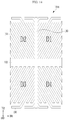
- a pixel electrode 191 A included in the display device according to the present exemplary embodiment has the same structure and features as most of the above-described pixel electrode 191 , however it may further include an edge portion 195 connected to or extending from the end portion of the branch electrode 194 and/or the longitudinal stem 193 .
- the edge portion 195 may extend in parallel with the first direction DR 1 along the edges of the upper and lower ends of the pixel electrode 191 A.
- the length of the first direction DR 1 of the edge portion 195 may be less than half the length of the first direction DR 1 of the pixel electrode 191 .
- the edge portion 195 may be connected to or extend from the end portions of two or more branch portions 194 among a plurality of branch portions 194 respectively disposed in four domains D 1 , D 2 , D 3 , and D 4 defined by the transverse stem 192 and the longitudinal stem 193 of the pixel electrode 191 A. Every other branch portion 194 may have the edge portion 195 disposed in four domains D 1 , D 2 , D 3 , and D 4 . Outmost edge portions 195 in four domains D 1 , D 2 , D 3 , and D 4 may extend to the edge of the pixel electrode 191 A in the first direction.
- a pixel electrode 191 B included in the display device according to the present exemplary embodiment is the same as most of the pixel electrode 191 A according to the exemplary embodiment shown in FIG. 13 , in that it includes an edge portion 196 connected to or extending from the end portion of the branch electrode 194 and/or the longitudinal stem 193 .
- the edge portion 196 may extend approximately in parallel to the first direction DR 1 along the edges of the upper and lower ends of the pixel electrode 191 B.
- the length of the first direction DR 1 of the edge portion 196 may be smaller than the length of the first direction DR 1 of the pixel electrode 191 .
- edge portion 196 may be connected to or extend from the end portion only of one branch portion 194 among the plurality of branch portions 194 respectively disposed in four domains D 1 , D 2 , D 3 , and D 4 defined by the transverse stem 192 and the longitudinal stem 193 of the pixel electrode 191 B. End of the edge portion 196 may extend to the edge of the pixel electrode 191 B in the first direction.
- a pixel electrode 191 C included in the display device according to the present exemplary embodiment is the same as most of the pixel electrodes 191 A and 191 B according to the exemplary embodiments shown in FIG. 13 or FIG. 14 , however it may further include an edge portion 198 disposed outside of the edge portions 195 and 196 .
- the edge portion 198 may be connected to or extend from the extending portion of the longitudinal stem 193 , and particularly may extend approximately parallel to the first direction DR 1 along the edges of the lower and upper ends of the pixel electrode 191 C.
- the length of the first direction DR 1 of the edge portion 198 may be substantially the same as the length of the first direction DR 1 of the pixel electrode 191 .
- FIG. 16 is a top plan view showing a part of one pixel of a display device according to an exemplary embodiment of the present inventive concept
- the display device according to the present exemplary embodiment may be substantially the same as most of the display device according to the exemplary embodiment described above, but the shape of the pixel electrode may be different.
- the branch electrode 194 of the pixel electrode may include the oblique portion 194 a and a transverse portion 194 e connected to or extending from the end of the oblique portion 194 a .
- the shape and characteristics of the transverse portion 194 e may be the same as the transverse portion 194 b of the above-described embodiment.
- the transverse portion 194 e according to the present embodiment may be disposed adjacent to the edge of the pixel electrode.
- the data line 171 may overlap the transverse portion 194 e of the pixel electrode 191 .
- the left and right edges of the data line 171 that are parallel to each other may overlap the transverse portion 194 e , or alternatively, only one of the left and right edges of the data line 171 may overlap the transverse portion 194 e.
- FIG. 17 is a variation of a cross-sectional view of a display device shown in FIG. 2 taken along a line IIIc-IIIb.
- the display device according to the present exemplary embodiment is mostly the same as the display device according to the above-described exemplary embodiment, but the color filter 230 may be disposed on the second display panel 200 instead of the first display panel 100 . That is, the plurality of color filters 230 may be disposed below the second substrate 210 , and the insulating layer 250 may be disposed below the plurality of color filters 230 .
- the light blocking member 220 described above may be disposed between the second substrate 210 and the insulating layer 250 .
- the light blocking member 220 may also be disposed in the first display panel 100 .
- FIG. 18 is a layout view of one pixel of a display device according to an exemplary embodiment of the present inventive concept
- FIG. 19 a cross-sectional view of a display device shown in FIG. 18 taken along a line XIXa-XIXb
- FIG. 20 is a cross-sectional view of a display device shown in FIG. 18 taken along a line XXa-XXb.
- the semiconductor layer may include a semiconductor 151 disposed between the data conductive layer including the data line 171 , the source electrode 173 , the plurality of drain electrodes 175 , and the gate insulating layer 140 .
- the semiconductor 151 includes a channel portion 154 a disposed between the source electrode 173 and the drain electrode 175 , as the channel of the thin film transistor Q. That is, the channel portion 154 a is not covered by the data conductive layer.
- An ohmic contact layer 161 may be disposed between the semiconductor 151 and the data conductive layer.
- the ohmic contact layer 161 may include ohmic contact layers 163 and 165 disposed under the source electrode 173 and the drain electrode 175 .
- the planar shape of the semiconductor 151 except for the channel portion 154 a and the ohmic contact layer 161 may be substantially similar to the planar shape of the data conductive layer. That is, the edge of the semiconductor 151 except the channel portion 154 a or the edge of the ohmic contact layer 161 except the channel portion 154 a may extend substantially parallel to the edge of the data conductive layer.
- the case where the signal line passing through the transmission region of the pixel electrode is the data line 171 has been described as a main example, but it is not limited thereto, and the present inventive concept may be equally applied to the case in which the data line 171 and/or other signal lines pass through the transmissive region of the pixel electrode.
Landscapes
- Physics & Mathematics (AREA)
- Nonlinear Science (AREA)
- General Physics & Mathematics (AREA)
- Chemical & Material Sciences (AREA)
- Crystallography & Structural Chemistry (AREA)
- Mathematical Physics (AREA)
- Optics & Photonics (AREA)
- Engineering & Computer Science (AREA)
- Microelectronics & Electronic Packaging (AREA)
- Geometry (AREA)
- Spectroscopy & Molecular Physics (AREA)
- Liquid Crystal (AREA)
- Devices For Indicating Variable Information By Combining Individual Elements (AREA)
Abstract
Description
Claims (20)
Applications Claiming Priority (2)
| Application Number | Priority Date | Filing Date | Title |
|---|---|---|---|
| KR1020190138741A KR102660294B1 (en) | 2019-11-01 | 2019-11-01 | Display device |
| KR10-2019-0138741 | 2019-11-01 |
Publications (2)
| Publication Number | Publication Date |
|---|---|
| US20210132456A1 US20210132456A1 (en) | 2021-05-06 |
| US11215892B2 true US11215892B2 (en) | 2022-01-04 |
Family
ID=75688932
Family Applications (1)
| Application Number | Title | Priority Date | Filing Date |
|---|---|---|---|
| US16/885,272 Active US11215892B2 (en) | 2019-11-01 | 2020-05-28 | Display device |
Country Status (3)
| Country | Link |
|---|---|
| US (1) | US11215892B2 (en) |
| KR (1) | KR102660294B1 (en) |
| CN (1) | CN112782894B (en) |
Citations (10)
| Publication number | Priority date | Publication date | Assignee | Title |
|---|---|---|---|---|
| US20100157232A1 (en) * | 2008-12-23 | 2010-06-24 | Samsung Electronics Co., Ltd | Array substrate and display device having the same |
| US20100182557A1 (en) * | 2009-01-21 | 2010-07-22 | Samsung Electronics Co., Ltd | Display substrate, display device having the same and method of manufacturing the display substrate |
| US20110242468A1 (en) * | 2010-04-02 | 2011-10-06 | Samsung Electronics Co., Ltd. | Pixel electrode panel, a liquid crystal display panel assembly and methods for manufacturing the same |
| KR101377169B1 (en) | 2012-06-01 | 2014-03-24 | 성균관대학교산학협력단 | Liquid crystal display apparatus and crystal display method |
| KR101502358B1 (en) | 2013-04-24 | 2015-03-13 | 삼성디스플레이 주식회사 | Liquid crystal display |
| KR20150039404A (en) | 2013-10-02 | 2015-04-10 | 삼성디스플레이 주식회사 | Thin film transistor substrate, liquid crystal display and and manufacturing method of thin film transistor substrate |
| US20150234240A1 (en) * | 2012-01-26 | 2015-08-20 | Samsung Display Co., Ltd. | Liquid crystal display |
| KR20150117414A (en) | 2014-04-10 | 2015-10-20 | 엘지디스플레이 주식회사 | Liquid crystal display device |
| US20160026050A1 (en) * | 2014-07-22 | 2016-01-28 | Au Optronics Corp. | Display panel and curved display |
| KR20160014851A (en) | 2014-07-29 | 2016-02-12 | 삼성디스플레이 주식회사 | Liquid crystal display device |
Family Cites Families (5)
| Publication number | Priority date | Publication date | Assignee | Title |
|---|---|---|---|---|
| CN102236220B (en) * | 2011-07-07 | 2013-11-06 | 深圳市华星光电技术有限公司 | Pixel electrode structure |
| JP5755710B2 (en) * | 2013-11-29 | 2015-07-29 | 株式会社ジャパンディスプレイ | Liquid crystal panel and electronic equipment |
| CN105158994B (en) * | 2015-09-30 | 2018-03-06 | 武汉华星光电技术有限公司 | Pixel cell and array base palte |
| KR102483751B1 (en) * | 2016-05-18 | 2023-01-02 | 삼성디스플레이 주식회사 | Liquid crystal display device |
| KR102495984B1 (en) * | 2018-03-22 | 2023-02-07 | 삼성디스플레이 주식회사 | Display device |
-
2019
- 2019-11-01 KR KR1020190138741A patent/KR102660294B1/en active Active
-
2020
- 2020-05-28 US US16/885,272 patent/US11215892B2/en active Active
- 2020-07-13 CN CN202010667901.1A patent/CN112782894B/en active Active
Patent Citations (11)
| Publication number | Priority date | Publication date | Assignee | Title |
|---|---|---|---|---|
| US20100157232A1 (en) * | 2008-12-23 | 2010-06-24 | Samsung Electronics Co., Ltd | Array substrate and display device having the same |
| US20100182557A1 (en) * | 2009-01-21 | 2010-07-22 | Samsung Electronics Co., Ltd | Display substrate, display device having the same and method of manufacturing the display substrate |
| KR20100085518A (en) | 2009-01-21 | 2010-07-29 | 삼성전자주식회사 | Display substrate, display device having the same, and method of manufacturing the display substrate |
| US20110242468A1 (en) * | 2010-04-02 | 2011-10-06 | Samsung Electronics Co., Ltd. | Pixel electrode panel, a liquid crystal display panel assembly and methods for manufacturing the same |
| US20150234240A1 (en) * | 2012-01-26 | 2015-08-20 | Samsung Display Co., Ltd. | Liquid crystal display |
| KR101377169B1 (en) | 2012-06-01 | 2014-03-24 | 성균관대학교산학협력단 | Liquid crystal display apparatus and crystal display method |
| KR101502358B1 (en) | 2013-04-24 | 2015-03-13 | 삼성디스플레이 주식회사 | Liquid crystal display |
| KR20150039404A (en) | 2013-10-02 | 2015-04-10 | 삼성디스플레이 주식회사 | Thin film transistor substrate, liquid crystal display and and manufacturing method of thin film transistor substrate |
| KR20150117414A (en) | 2014-04-10 | 2015-10-20 | 엘지디스플레이 주식회사 | Liquid crystal display device |
| US20160026050A1 (en) * | 2014-07-22 | 2016-01-28 | Au Optronics Corp. | Display panel and curved display |
| KR20160014851A (en) | 2014-07-29 | 2016-02-12 | 삼성디스플레이 주식회사 | Liquid crystal display device |
Also Published As
| Publication number | Publication date |
|---|---|
| CN112782894B (en) | 2024-12-03 |
| US20210132456A1 (en) | 2021-05-06 |
| KR20210053393A (en) | 2021-05-12 |
| CN112782894A (en) | 2021-05-11 |
| KR102660294B1 (en) | 2024-04-24 |
Similar Documents
| Publication | Publication Date | Title |
|---|---|---|
| US10663813B2 (en) | Liquid crystal display | |
| US9780177B2 (en) | Thin film transistor array panel including angled drain regions | |
| US10811437B2 (en) | Display device including pixel electrode having multiple domains | |
| US9530364B2 (en) | Liquid crystal display | |
| KR102074424B1 (en) | Liquid crystal display and manufacturing method thereof | |
| KR101237011B1 (en) | Liquid crystal display | |
| US10394091B2 (en) | Liquid crystal display device | |
| WO2004017129A1 (en) | Pixel array for display device and liquid crystal display | |
| KR20150029377A (en) | Display device | |
| KR101267496B1 (en) | Liquid crystal display | |
| US20210193697A1 (en) | Display device and manufacturing method thereof | |
| US7973865B2 (en) | Thin film transistor display plate and liquid crystal display having the same | |
| US9891485B2 (en) | Liquid crystal display | |
| US11215892B2 (en) | Display device | |
| US11579502B2 (en) | Display device | |
| KR102109678B1 (en) | Liquid crystal display | |
| US20160202557A1 (en) | Liquid crystal display and method of manufacturing the same | |
| KR20210123463A (en) | Liquid crystal display device | |
| KR20060084014A (en) | Thin film transistor array panel and display device using same | |
| KR20080067485A (en) | Liquid crystal display | |
| KR20090002817A (en) | Liquid crystal display |
Legal Events
| Date | Code | Title | Description |
|---|---|---|---|
| AS | Assignment |
Owner name: SAMSUNG DISPLAY CO., LTD., KOREA, REPUBLIC OF Free format text: ASSIGNMENT OF ASSIGNORS INTEREST;ASSIGNORS:SHIN, KYEONG HWAN;AHN, KYU SU;YOO, DONG IL;SIGNING DATES FROM 20200224 TO 20200522;REEL/FRAME:052769/0307 |
|
| FEPP | Fee payment procedure |
Free format text: ENTITY STATUS SET TO UNDISCOUNTED (ORIGINAL EVENT CODE: BIG.); ENTITY STATUS OF PATENT OWNER: LARGE ENTITY |
|
| STPP | Information on status: patent application and granting procedure in general |
Free format text: RESPONSE TO NON-FINAL OFFICE ACTION ENTERED AND FORWARDED TO EXAMINER |
|
| STPP | Information on status: patent application and granting procedure in general |
Free format text: FINAL REJECTION MAILED |
|
| STPP | Information on status: patent application and granting procedure in general |
Free format text: ADVISORY ACTION MAILED |
|
| STPP | Information on status: patent application and granting procedure in general |
Free format text: DOCKETED NEW CASE - READY FOR EXAMINATION |
|
| STPP | Information on status: patent application and granting procedure in general |
Free format text: NOTICE OF ALLOWANCE MAILED -- APPLICATION RECEIVED IN OFFICE OF PUBLICATIONS |
|
| STPP | Information on status: patent application and granting procedure in general |
Free format text: PUBLICATIONS -- ISSUE FEE PAYMENT VERIFIED |
|
| STCF | Information on status: patent grant |
Free format text: PATENTED CASE |
|
| MAFP | Maintenance fee payment |
Free format text: PAYMENT OF MAINTENANCE FEE, 4TH YEAR, LARGE ENTITY (ORIGINAL EVENT CODE: M1551); ENTITY STATUS OF PATENT OWNER: LARGE ENTITY Year of fee payment: 4 |