US11215775B2 - Connection features for electronic and optical packaging - Google Patents
Connection features for electronic and optical packaging Download PDFInfo
- Publication number
- US11215775B2 US11215775B2 US16/544,699 US201916544699A US11215775B2 US 11215775 B2 US11215775 B2 US 11215775B2 US 201916544699 A US201916544699 A US 201916544699A US 11215775 B2 US11215775 B2 US 11215775B2
- Authority
- US
- United States
- Prior art keywords
- optical
- fastener
- feature
- photonic element
- optical connector
- Prior art date
- Legal status (The legal status is an assumption and is not a legal conclusion. Google has not performed a legal analysis and makes no representation as to the accuracy of the status listed.)
- Active
Links
Images


Classifications
-
- G—PHYSICS
- G02—OPTICS
- G02B—OPTICAL ELEMENTS, SYSTEMS OR APPARATUS
- G02B6/00—Light guides; Structural details of arrangements comprising light guides and other optical elements, e.g. couplings
- G02B6/24—Coupling light guides
- G02B6/42—Coupling light guides with opto-electronic elements
- G02B6/4201—Packages, e.g. shape, construction, internal or external details
- G02B6/4219—Mechanical fixtures for holding or positioning the elements relative to each other in the couplings; Alignment methods for the elements, e.g. measuring or observing methods especially used therefor
- G02B6/4228—Passive alignment, i.e. without a detection of the degree of coupling or the position of the elements
- G02B6/423—Passive alignment, i.e. without a detection of the degree of coupling or the position of the elements using guiding surfaces for the alignment
-
- G—PHYSICS
- G02—OPTICS
- G02B—OPTICAL ELEMENTS, SYSTEMS OR APPARATUS
- G02B6/00—Light guides; Structural details of arrangements comprising light guides and other optical elements, e.g. couplings
- G02B6/24—Coupling light guides
- G02B6/36—Mechanical coupling means
- G02B6/38—Mechanical coupling means having fibre to fibre mating means
- G02B6/3807—Dismountable connectors, i.e. comprising plugs
- G02B6/3897—Connectors fixed to housings, casing, frames or circuit boards
-
- G—PHYSICS
- G02—OPTICS
- G02B—OPTICAL ELEMENTS, SYSTEMS OR APPARATUS
- G02B6/00—Light guides; Structural details of arrangements comprising light guides and other optical elements, e.g. couplings
- G02B6/24—Coupling light guides
- G02B6/42—Coupling light guides with opto-electronic elements
- G02B6/4201—Packages, e.g. shape, construction, internal or external details
- G02B6/4219—Mechanical fixtures for holding or positioning the elements relative to each other in the couplings; Alignment methods for the elements, e.g. measuring or observing methods especially used therefor
- G02B6/4236—Fixing or mounting methods of the aligned elements
-
- G—PHYSICS
- G02—OPTICS
- G02B—OPTICAL ELEMENTS, SYSTEMS OR APPARATUS
- G02B6/00—Light guides; Structural details of arrangements comprising light guides and other optical elements, e.g. couplings
- G02B6/24—Coupling light guides
- G02B6/42—Coupling light guides with opto-electronic elements
- G02B6/4292—Coupling light guides with opto-electronic elements the light guide being disconnectable from the opto-electronic element, e.g. mutually self aligning arrangements
-
- G—PHYSICS
- G02—OPTICS
- G02B—OPTICAL ELEMENTS, SYSTEMS OR APPARATUS
- G02B6/00—Light guides; Structural details of arrangements comprising light guides and other optical elements, e.g. couplings
- G02B6/24—Coupling light guides
- G02B6/42—Coupling light guides with opto-electronic elements
- G02B6/4201—Packages, e.g. shape, construction, internal or external details
- G02B6/4204—Packages, e.g. shape, construction, internal or external details the coupling comprising intermediate optical elements, e.g. lenses, holograms
- G02B6/4212—Packages, e.g. shape, construction, internal or external details the coupling comprising intermediate optical elements, e.g. lenses, holograms the intermediate optical element being a coupling medium interposed therebetween, e.g. epoxy resin, refractive index matching material, index grease, matching liquid or gel
-
- G—PHYSICS
- G02—OPTICS
- G02B—OPTICAL ELEMENTS, SYSTEMS OR APPARATUS
- G02B6/00—Light guides; Structural details of arrangements comprising light guides and other optical elements, e.g. couplings
- G02B6/24—Coupling light guides
- G02B6/42—Coupling light guides with opto-electronic elements
- G02B6/4201—Packages, e.g. shape, construction, internal or external details
- G02B6/4249—Packages, e.g. shape, construction, internal or external details comprising arrays of active devices and fibres
Definitions
- Embodiments presented in this disclosure generally relate to streamlining the addition of mechanical features to secure electronic and optical packages.
- Electronics and optical components are often joined together to provide connectivity between various other electronic and optical components creating electronic and optical packages. These packages frequently include additional parts to ensure proper functioning of the joined parts in the packages.
- the electronic and optical packages may include the addition of heat sinks, mechanical supports, clamps, housings, and other structures around the chips and boards in the packages. These additional parts are useful to provide mechanical stability, pass necessary reliability testing, and enable adequate cooling and heat transfer.
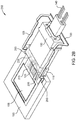
- FIG. 1 illustrates an expanded view of an example optical connection assembly, according to embodiments described herein.
- FIG. 2A illustrates an optical connection assembly with an optical adapter, according to embodiments described herein.
- FIG. 2B illustrates an optical connection assembly with an optical adapter, according to embodiments described herein.
- FIG. 3A illustrates an optical connection assembly without an optical adapter, according to embodiments described herein.
- FIG. 3B illustrates a photonic connection assembly, according to embodiments described herein.
- FIGS. 4A-B illustrate detailed views of fasteners for example optical assemblies, according to embodiments described herein.
- FIGS. 5A-B illustrate detailed views of a mechanical connection feature for example optical assemblies, according to embodiments described herein.
- FIGS. 6A-G illustrate various views of the fabrication of an optical connection assembly, according to embodiments described herein.
- FIG. 7 is a flow chart outlining general operations in an example method to produce an optical connection assembly, according to embodiments described herein.
- An example embodiment includes an optical connection assembly, including: a framing component including a mechanical connection feature; a photonic element including an optical feature, where the photonic element is affixed to the framing component.
- the optical connection assembly also includes an optical connector optically connected to the optical feature in the photonic element, where the optical connector includes an external contact point; and a fastener affixed to the framing component via the mechanical connection feature, where the fastener is joined to the external contact point to establish a mechanical connection between the optical connector and the photonic element.
- An example embodiment includes a photonic connection assembly, including: a photonic element including an optical feature and a connection feature; an optical connector optically connected to the optical feature in the photonic element, where the optical connector includes an external contact point; and a fastener affixed to the photonic element via the connection feature, where the fastener is joined to the external contact point to secure the optical connector to the photonic element.
- One general aspect includes a method for manufacturing an optical connection assembly.
- the method includes: affixing a photonic element and a mechanical connection feature to a carrier layer; forming a framing layer by covering the photonic element and the mechanical connection feature with a framing mold; removing a portion of the framing mold, where the removal of the portion exposes a bottom side of the photonic element and a bottom side of the mechanical connection feature; removing the carrier layer to form a die including the photonic element, the mechanical connection feature, and the framing layer; attaching an optical connector to the die to form an optical connection; joining a fastener to the optical connector; and affixing the fastener to the die via the mechanical connection feature.
- the electronic and optical packages are frequently created to provide connections between various electronic and optical components.
- the electronic and optical packages include additional structures such as heat sinks, mechanical supports, clamps, housings, and other structures around the chips and boards in the packages. These parts provide mechanical stability such as securing the components of the packages to each other.
- etching and drilling into dies and boards can be challenging due to mechanical tolerancing limitations (e.g., limited control of hole position, depth, and size) and also due to the risk of causing cracks or damage on the components. Additionally, some processes such as deep reactive ion etching (DRIE) are limited to producing holes/mechanical features of up to a few hundred microns deep.
- DRIE deep reactive ion etching
- the assemblies and methods described herein use Fan Out Wafer Level Packaging (FOWLP) processes to streamline the addition of mechanical components (e.g., a fastener, etc.) onto optical and electronics packages.
- FOWLP processes provide a method to add mechanical connection and other features directly to a reconstituted die without the introduction of mechanical processes to fragile optical components.
- the resulting assemblies provide mechanical/structural support to the optical packages to ensure an optical connection between the components is maintained.
- FIG. 1 illustrates an expanded view of an example optical connection assembly, according to embodiments described herein.
- the optical connection assembly, assembly 100 includes the framing component, mold compound 150 and a photonic element 155 .
- the mold compound 150 is a FOWLP frame or reconstituted die formed from an epoxy material which is cured to form reconstituted dies, where the mold compound 150 provides a frame/support for the photonic element 155 .
- the mold compound 150 is formed in processes described in relation to FIGS. 6A-6G .
- the photonic element 155 includes a Photonic Integrated Circuit (PIC) including optical features 160 and/or an Electrical Integrated Circuit (EIC) as part of the mold compound 150 .
- the photonic element 155 is an optical device that may operate to amplify, dim, extinguish, phase shift, switch, modulate, direct optical signals, and convert optical signals to an electrical signal for use by an EIC integrated with or connected to the photonic element 155 .
- the EIC is an electrical circuit that operates with the optical connection assembly described herein to send or receive and process optical signals.
- the EIC may include a processor, memory storage devices, communications interfaces to other electrical circuits or equipment, and components to drive or receive optical signals via an optical connection assembly including the photonic element 155 .
- the photonic element 155 optically interfaces with the optical adapter 115 and/or the optical connector 130 to carry optical signals from the photonic element 155 to external devices or to the photonic element 155 from external devices via fibers 140 .
- the interfaces between the photonic element 155 , the optical adapter 115 , and/or the optical connector 130 includes an index matching epoxy applied to improve the optical coupling between the various elements.
- the photonic element 155 is aligned and affixed to the mold compound 150 using one or more reference points on the photonic element, such as fiducials and one or more reference points on the mold compound 150 , etc.
- the optical features 160 include one or more waveguides in the substrate of the photonic element 155 , where the one or more waveguides are connected to an electrical and/or optical component integrated within the photonic element 155 .
- the assembly 100 also includes mechanical features 110 which provide a connection point for a fastener.
- the mechanical features 110 include prefabricated and/or drilled holes/slots in the mold compound 150 , where the holes/slots are added in the FOWLP process described in relation to FIGS. 6A-6G below.
- the mechanical features 110 provide a mechanical connection point for a fastener 105 (e.g., a clamp piece) including the mechanical attachment portion(s) and/or insertion sections, peg(s) 107 .
- the fastener 105 is attached to the mold compound 150 by the pegs 107 being inserted into the mechanical features 110 .
- the pegs 107 are further held in place in the mechanical features 110 by an additional joining material such as an adhesive, an epoxy, solder, etc. applied to the pegs 107 and the mechanical features(s) 110 . Additional fasteners and mechanical connection features are described in relation to FIGS. 4A-5B .
- the assembly 100 also includes the optical connector 130 which includes components to provide an optical connection between fibers 140 and the optical features 160 .
- the optical connector 130 includes alignment components 135 (e.g., pins) which assist in the mechanical alignment of the optical connector 130 to the mold compound 150 and the photonic element 155 .
- the optical connector 130 may also include one or more external contact points 132 .
- the external contact points 132 include standard features of the optical connector 130 and/or customized features added to the optical connector 130 to provide a contact point for the fastener 105 .
- the optical connector 130 is a standard Multi-fiber Push On (MPO) connector.
- MPO Multi-fiber Push On
- the fastener 105 may be formed from any material that can provide structural support and keep the components joined including molded plastic, molded metal, and/or wire.
- the fastener 105 leverages the mechanical connection features in the mold compound 150 (holes, slots, etc.) and on the contact points on a standard optical connector to help hold the connector in place using retention force.
- the fastener 105 may include features to generate spring forces for retention (e.g., spring sections etc.).
- the fastener 105 may also be unjoined/removed from the external contact points 132 when a force is applied to the fastener, thus allowing the optical assembly to be taken apart and/or updated.
- the assembly 100 also includes an optical adapter 115 which may be positioned in order to aid the optical connection between the optical connector 130 and the photonic element 155 .
- the optical adapter 115 may include a silicon dioxide (SiO 2 ) type glass (e.g., borofloat, borosilicate, etc.), where the silicon-oxygen bonds in the SiO 2 type glass.
- the optical adapter 115 provides additional support and/or structure for the connection between the optical connector 130 and the photonic element 155 .
- the optical adapter 115 includes the adapter optical features, waveguides 125 , to provide an optical connection between the optical connector 130 and the optical features 160 of the photonic element 155 . While assembly 100 described in relation to FIG. 1 includes a single mold compound 150 , fastener 105 , and photonic element 155 the assembly 100 may include multiple dies, fasteners, and photonic/electronic elements connected to multiple optical and electrical connectors.
- FIG. 2A illustrates an optical connection assembly, according to embodiments described herein.
- the optical connection assembly 200 includes the components of assembly 100 discussed in relation to assembly 100 in FIG. 1 arranged as a connected optical connection assembly 200 .
- the fastener 105 is affixed to the mold compound 150 at the connections 210 .
- the fastener 105 is affixed to the mold compound 150 by inserting the pegs 107 in the mechanical features 110 along with an adhesive where the adhesive and the peg 107 provide the connection 210 .
- the optical connection assembly 200 includes the optical adapter 115 affixed/disposed on the topside of the photonic element 155 /mold compound 150 to provide additional structural support to the connection between the photonic element 155 and the optical connector 130 .
- the optical adapter 115 is affixed to the photonic element using an index matching epoxy to provide optical coupling between the optical adapter 115 and the photonic element 155 .
- the optical adapter 115 includes the alignment features 235 (e.g., pin holes that mate with the pins of the optical connector 130 ).
- the optical adapter and the photonic element 155 together form the alignment features 235 .
- the alignment features 235 include defined alignment paths/slats, pin holes, etc. that receive the alignment components 135 (pins) and aligns the optical connector 130 to the optical features 160 shown in FIG. 1 .
- This positioning of the fastener 105 secures the optical connector 130 to the photonic element 155 and the mold compound 150 to ensure the optical connection remains connected.
- the fastener 105 may also be unjoined/removed from the external contact points 132 when a force is applied to the fastener, thus allowing the optical assembly to be taken apart and/or updated. For example, a downward force on the fastener 105 shown in FIG. 2A unjoins the fastener 105 from the optical connector 130 and allows for the optical connector 130 to be easily removed from the assembly.
- FIG. 2B illustrates an optical connection assembly, according to embodiments described herein.
- the optical connection assembly 250 includes the components of assembly 100 discussed in relation to assembly 100 in FIG. 1 arranged as a connected optical connection assembly 250 .
- the fastener 105 is affixed to the mold compound 150 at the connections 260 .
- the fastener 105 is affixed to the mold compound 150 by inserting the pegs 107 in the mechanical features 110 along with an adhesive where the adhesive and the peg 107 provide the connection 260 .
- the optical connection assembly 250 includes the optical adapter 115 affixed and/or butt-coupled on a side of the photonic element 155 /mold compound 150 to provide a connection between the photonic element 155 and the optical connector 130 .
- the optical adapter 115 is affixed to the photonic element using an index matching epoxy to provide optical coupling between the optical adapter 115 and the photonic element 155 .
- the optical adapter 115 and the optical support 215 are affixed to the photonic element 155 and the mold compound 150 , where the optical support 215 provides additional structural support to the optical adapter 115 when butt-coupled to a side of the photonic element 155 .
- the optical adapter 115 shown in FIG. 2B includes the alignment features 235 which receive the alignment components 135 and aligns the optical connector 130 to the waveguides 125 shown in FIG. 1 , where the waveguides 125 are optically connected to the optical features 160 .
- the fastener 105 is positioned to the arrangement shown in FIG. 2B where the fastener 105 is positioned around the optical connector 130 , and where an attachment portion 120 of the fastener 105 is joined to the optical connector 130 at the external contact points 132 . This positioning of the fastener 105 secures the optical connector 130 to the optical adapter 115 to ensure the optical connection remains connected.
- the fastener 105 may also be unjoined/removed from the external contact points 132 when a force is applied to the fastener, thus allowing the optical assembly to be taken apart and/or updated. For example, a downward force on the fastener 105 shown in FIG. 2B unjoins the fastener 105 from the optical connector 130 and allows for the optical connector 130 to be easily removed from the assembly.
- FIG. 3A illustrates an optical connection assembly, according to embodiments described herein.
- the optical connection assembly 300 includes the components of assembly 100 discussed in relation to assembly 100 in FIG. 1 arranged as a connected optical connection assembly 300 without an optical adapter thus providing a direct connection between the optical connector 103 and the optical features 160 .
- the fastener 105 is affixed to the mold compound 150 at the connections 310 in a manner similar to connections 210 as described in FIG. 2A .
- the photonic element 155 includes the alignment features 335 .
- the alignment features 335 include defined alignment paths/slats etc. directly in the photonic element 155 that receive the alignment components 135 and aligns the optical connector 130 to the optical features 160 shown in FIG. 1 .
- the fastener 105 is positioned to the arrangement shown in FIG. 3A where an attachment portion 120 of the fastener 105 is joined to the optical connector 130 at the external contact points 132 .
- This positioning of the fastener 105 secures the optical connector 130 to the photonic element 155 and the mold compound 150 to ensure the optical connection remains connected.
- the fastener 105 may also be unjoined/removed from the external contact points 132 when a force is applied to the fastener, thus allowing the optical assembly to be taken apart and/or updated. For example, a downward force on the fastener 105 shown in FIG. 3A unjoins the fastener 105 from the optical connector 130 and allows for the optical connector 130 to be easily removed from the assembly.
- FIG. 3B illustrates a photonic connection assembly, according to embodiments described herein.
- the optical connection assemblies includes the mold compound 150 .
- the photonic assembly 350 includes the fastener 105 directly attached to the photonic element 155 eliminating the need for the mold compound 150 .
- the fastener 105 is affixed to the photonic element 155 one or more connection features 360 .
- the connection features 360 may include connection pads configured for the attachment portions 365 .
- the attachment portions 365 may be directly epoxied to the connection pads.
- the connection features 360 include mechanically defined features such as hole or slats.
- the photonic element 155 includes the alignment features 335 including defined alignment paths/slats etc. directly in the photonic element 155 that receive the alignment components 135 and aligns the optical connector 130 to the optical features 160 shown in FIG. 1 .
- the fastener is positioned to the arrangement shown in FIG. 3B where the fastener 105 is positioned around the optical connector 130 , where an attachment portion 120 of the fastener 105 is joined to the optical connector 130 at the external contact points 132 . This positioning of the fastener 105 secures the optical connector 130 to the photonic element 155 to ensure the optical connection remains connected. As described in FIGS.
- the fastener 105 may also be unjoined/removed from the external contact points 132 when a force is applied to the fastener, thus allowing the optical assembly to be taken apart and/or updated.
- a downward force on the fastener 105 shown in FIG. 3B unjoins the fastener 105 from the optical connector 130 and allows for the optical connector 130 to be easily removed from the assembly.
- the photonic assembly 350 may also include an optical adapter and optical support as described in FIGS. 2A-2B .
- FIGS. 4A-B illustrate detailed views of fasteners for example optical assemblies, according to embodiments described herein.
- the optical assembly 400 may include any of the optical assemblies 200 , 250 , 300 , and 350 described in relation to FIGS. 2A-3B with a fastener 405 .
- FIG. 4A illustrates a top view of the optical assembly 400 and the fastener 405 , where the fastener 405 includes two clamp pieces, each of the two clamp pieces include an attachment portion 406 .
- the attachment portions 406 are joined to the optical connector 130 at the one or more external contact points 132 .
- the fastener 405 includes springs configured to apply a retention/retaining force at the external contact points 132 to secure the optical connector 130 to the photonic element 155 and/or the mold compound 150 .
- the spring also allow for the fastener 405 to be unjoined/removed from the external contact points 132 when a force is applied to the fastener, thus allowing the optical assembly to be easily taken apart and/or updated.
- the fastener 405 may be positioned around the sides of the optical connector 130 and to the external contact points 132 .
- FIG. 4B illustrates a side view of the optical assembly 400 and the fastener 405 . As shown in FIG. 4B , the fastener 405 may be positioned about the top of the optical connector 130 and to the external contact points 132 .
- FIGS. 5A-B illustrate detailed views of a mechanical connection feature for example optical assemblies, according to embodiments described herein.
- the mechanical connection feature 510 extends horizontally through the mold compound 150 .
- the fastener 505 is affixed to the mold compound 150 by passing through the mechanical connection feature 510 .
- FIGS. 6A-G illustrate various views of the fabrication of an optical connection assembly, according to embodiments described herein.
- FIG. 6A illustrates a top and side view of a first step 600 in the fabrication of an optical assembly.
- a photonic element and one or more mechanical connection features are attached/affixed to a carrier layer.
- a top side of the photonic element 155 and the mechanical feature 110 are attached to the carrier 605 .
- a plurality of photonic elements 155 and mechanical features 110 are attached to a wafer of the carrier 605 to create multiple arrangements 606 of the photonic elements and mechanical features.
- attaching/affixing the photonic elements 155 and mechanical features 110 is done with a standard FOWLP process to place photonics dies and other components onto a sticky tape or carrier wafer.
- the mechanical features 110 include preformed hole/slot structures that are affixed to the carrier 605 .
- the mechanical features may include a portion 607 which covers the mechanical feature 110 to prevent a framing mold from entering the mechanical features 110 .
- FIG. 6B illustrates a top and side view of a second step 610 in the fabrication of an optical assembly.
- a framing layer 615 is formed by covering the photonic element 155 and the one or more mechanical connection features with a framing mold.
- the framing mold fills the areas between the photonic element 155 and the mechanical features 110 to form the framing layer 615 .
- FIG. 6C illustrates a top and side view of a third step 620 in the fabrication of an optical assembly.
- a portion 621 of the framing mold/layer 615 is removed.
- the portion 621 is mechanically ground to remove the portion 621 of mold compound and expose the hole structures/bottom side of the mechanical features 110 (e.g., removing portion 607 ) and backside/bottom side of the photonic element 155 .
- FIG. 6D illustrates a top and side view of a fourth step 630 in the fabrication of an optical assembly.
- the carrier 605 is removed to form a die 632 .
- each die 632 includes the photonic element 155 , the one or more mechanical connection features, mechanical features 110 , and the remaining framing layer 615 .
- the carrier 605 is removed at the wafer-level and the plurality of arrangements 606 are diced into a plurality of dies 632 .
- additional processing to form vias, redistribution layers, and/or other electronics structures are completed prior to dicing the dies 632 .
- FIG. 6E illustrates top views of various fifth steps 640 a , 640 b , and 640 c in the fabrication of an optical assembly.
- the dies 632 a - 632 c are further processed using standard fabrication processes to complete any additional opto-mechanical assembly needed (e.g., chip attach, laser attach, etc.).
- alignment features 641 e.g., pin holes
- the contact pads and/or connection features 360 are added to the photonic element 155 using standard fabrication processes.
- the dies 632 b and 632 c are too thin to support alignment features directly in the photonic element 155 .
- an optical adapter 115 is affixed to the die at steps 640 b and 640 c .
- the optical adapter includes alignment features 642 formed in the adapters prior to affixing the optical adapter 115 to the dies.
- the optical adapter 115 is disposed/affixed to on a top portion of the photonic element 155 . For example, the optical adapter 115 is placed on the die 132 b to form a socket in combination with existing pin holes on the die.
- optical adapter 115 is actively aligned/affixed to a side of the die 632 c by a butt-coupling process using an index matching epoxy.
- an optical support 215 as shown in FIG. 2B is also affixed to the die 632 c to provide additional structural support to the optical adapter 115 .
- FIG. 6F illustrates top views of various sixth steps 650 a , 650 b , and 650 c in the fabrication of an optical assembly.
- steps 650 a , 650 b , and 650 c an optical connector 130 is attached to the dies 632 a - 632 c to form an optical connection.
- the optical connector 130 and the alignment components 135 are aligned with the photonic element 155 and connected to provide the optical connection between the optical features 160 and the fibers 140 .
- the optical connector 130 and the alignment components 135 are connected to the photonic element using the optical adapter 115 .
- FIG. 6G illustrates a seventh step 660 in the fabrication of an optical assembly.
- a fastener 105 about the optical connector 130 and affixed to the die via the one or more mechanical connection features, mechanical features 110 .
- the pegs 107 of the fastener 105 are inserted into the holes of the mechanical features 110 made during previous steps allowing the fastener surrounding the optical connector 130 to securely hold the fiber connector in place.
- step 660 includes adding an epoxy, solder, and/or other joining material component to the mechanical features 110 and/or the fastener 105 to hold the fastener in place. While shown with an optical adapter in FIG.
- the fastener 105 is affixed to the dies 132 a - 132 c in a similar manner to form the various connections 210 , 260 , 310 , and 365 described in relation to FIGS. 2A-3B .
- FIG. 7 is a flow chart outlining general operations in an example method to produce an optical connection assembly, according to embodiments described herein. Reference will be made to previous figures.
- Method 700 begins at block 702 where a photonic element and a mechanical connection feature are affixed to a carrier layer such as shown in step 600 of FIG. 6A .
- the carrier includes a carrier layer wafer, where a plurality of photonic elements and mechanical connection features are affixed to the carrier layer as also shown in FIG. 6A .
- a framing layer is formed by covering the photonic element and the mechanical connection feature with a framing mold as shown in step 610 in FIG. 6B .
- a portion of the framing mold is removed.
- the portion 621 at step 620 in FIG. 6C is removed from the framing mold.
- the removal of the portion 621 exposes a bottom side of the photonic element 155 and a bottom side of the mechanical connection feature 110 .
- the carrier layer is removed to form a die where the die includes the photonic element, the mechanical connection feature, and the framing layer.
- removing the carrier layer also includes removing the carrier layer from the plurality of photonic elements, mechanical connection features, and framing layer of the carrier layer wafer and dicing the framing layer into single dies as shown in step 630 of FIG. 6D .
- an optical connector is attached to the die to form an optical connection.
- attaching the optical connector may also include affixing an optical adapter to the die, such as on disposing and affixing the optical adapter on the photonic element and/or butt-coupling the optical adapter to a side of the photonic element and the die as described in steps 640 b and 640 c of FIG. 6E .
- a fastener is joined to the optical connector and at block 714 , the fastener is affixed to the die via the mechanical connection feature.
- the fastener 105 is joined to the optical connector 130 at the attachment portion 120 and the external contact points 132 .
- the fastener 105 is also affixed to the mold compound 150 at the mechanical features 110 .
- the fastener 105 is affixed/epoxied to the mold compound 150 prior to connecting the optical connector 130 .
Landscapes
- Physics & Mathematics (AREA)
- General Physics & Mathematics (AREA)
- Optics & Photonics (AREA)
- Optical Couplings Of Light Guides (AREA)
- Mechanical Coupling Of Light Guides (AREA)
Abstract
Description
Claims (18)
Priority Applications (1)
| Application Number | Priority Date | Filing Date | Title |
|---|---|---|---|
| US16/544,699 US11215775B2 (en) | 2019-08-19 | 2019-08-19 | Connection features for electronic and optical packaging |
Applications Claiming Priority (1)
| Application Number | Priority Date | Filing Date | Title |
|---|---|---|---|
| US16/544,699 US11215775B2 (en) | 2019-08-19 | 2019-08-19 | Connection features for electronic and optical packaging |
Publications (2)
| Publication Number | Publication Date |
|---|---|
| US20210055489A1 US20210055489A1 (en) | 2021-02-25 |
| US11215775B2 true US11215775B2 (en) | 2022-01-04 |
Family
ID=74647201
Family Applications (1)
| Application Number | Title | Priority Date | Filing Date |
|---|---|---|---|
| US16/544,699 Active US11215775B2 (en) | 2019-08-19 | 2019-08-19 | Connection features for electronic and optical packaging |
Country Status (1)
| Country | Link |
|---|---|
| US (1) | US11215775B2 (en) |
Families Citing this family (2)
| Publication number | Priority date | Publication date | Assignee | Title |
|---|---|---|---|---|
| US11320610B2 (en) | 2020-04-07 | 2022-05-03 | Cisco Technology, Inc. | Integration of power and optics through cold plate for delivery to electronic and photonic integrated circuits |
| US11307368B2 (en) | 2020-04-07 | 2022-04-19 | Cisco Technology, Inc. | Integration of power and optics through cold plates for delivery to electronic and photonic integrated circuits |
Citations (13)
| Publication number | Priority date | Publication date | Assignee | Title |
|---|---|---|---|---|
| US7349223B2 (en) | 2000-05-23 | 2008-03-25 | Nanonexus, Inc. | Enhanced compliant probe card systems having improved planarity |
| US20120121218A1 (en) * | 2010-11-15 | 2012-05-17 | Electronics And Telecommunications Research Institute | Photonics chip and optical apparatus including the same |
| US8421212B2 (en) | 2010-09-22 | 2013-04-16 | Stats Chippac Ltd. | Integrated circuit packaging system with active surface heat removal and method of manufacture thereof |
| US20140153876A1 (en) * | 2012-06-13 | 2014-06-05 | Tyco Electronics Netherland Bv | Cable fixture assembly for fastening at least one cable at a cable carrier as well as a splitter comprising such cable fixture assembly |
| US9123685B2 (en) | 2013-07-15 | 2015-09-01 | Freescale Semiconductor Inc. | Microelectronic packages having frontside thermal contacts and methods for the fabrication thereof |
| US20160070048A1 (en) * | 2014-09-05 | 2016-03-10 | Schott Ag | Apparatus for connecting a fiber optic or rigid light guide to a light source |
| US20170097482A1 (en) * | 2015-10-05 | 2017-04-06 | Sumitomo Electric Industries, Ltd. | Connecting optical part, optical processing apparatus, methods for fabricating connecting optical part, method for fabricating guide member product |
| US20170271229A1 (en) | 2016-03-21 | 2017-09-21 | Infineon Technologies Ag | Spatially selective roughening of encapsulant to promote adhesion with functional structure |
| US20170343738A1 (en) * | 2015-05-29 | 2017-11-30 | Corning Optical Communications LLC | Optical connectors and optical couplings for fiber-to-photonics circuit connections |
| US20170343747A1 (en) * | 2016-05-27 | 2017-11-30 | Corning Optical Communications LLC | Silicon-based optical ports providing passive alignment connectivity |
| US20180180826A1 (en) * | 2015-06-15 | 2018-06-28 | Rwth Aachen | Self-alignment for apparatus comprising photonic device |
| US10163750B2 (en) | 2016-12-05 | 2018-12-25 | Taiwan Semiconductor Manufacturing Company, Ltd. | Package structure for heat dissipation |
| US20190384007A1 (en) * | 2017-03-07 | 2019-12-19 | Corning Optical Communications LLC | Universal photonic adaptor for coupling an optical connector to an optoelectronic substrate |
-
2019
- 2019-08-19 US US16/544,699 patent/US11215775B2/en active Active
Patent Citations (13)
| Publication number | Priority date | Publication date | Assignee | Title |
|---|---|---|---|---|
| US7349223B2 (en) | 2000-05-23 | 2008-03-25 | Nanonexus, Inc. | Enhanced compliant probe card systems having improved planarity |
| US8421212B2 (en) | 2010-09-22 | 2013-04-16 | Stats Chippac Ltd. | Integrated circuit packaging system with active surface heat removal and method of manufacture thereof |
| US20120121218A1 (en) * | 2010-11-15 | 2012-05-17 | Electronics And Telecommunications Research Institute | Photonics chip and optical apparatus including the same |
| US20140153876A1 (en) * | 2012-06-13 | 2014-06-05 | Tyco Electronics Netherland Bv | Cable fixture assembly for fastening at least one cable at a cable carrier as well as a splitter comprising such cable fixture assembly |
| US9123685B2 (en) | 2013-07-15 | 2015-09-01 | Freescale Semiconductor Inc. | Microelectronic packages having frontside thermal contacts and methods for the fabrication thereof |
| US20160070048A1 (en) * | 2014-09-05 | 2016-03-10 | Schott Ag | Apparatus for connecting a fiber optic or rigid light guide to a light source |
| US20170343738A1 (en) * | 2015-05-29 | 2017-11-30 | Corning Optical Communications LLC | Optical connectors and optical couplings for fiber-to-photonics circuit connections |
| US20180180826A1 (en) * | 2015-06-15 | 2018-06-28 | Rwth Aachen | Self-alignment for apparatus comprising photonic device |
| US20170097482A1 (en) * | 2015-10-05 | 2017-04-06 | Sumitomo Electric Industries, Ltd. | Connecting optical part, optical processing apparatus, methods for fabricating connecting optical part, method for fabricating guide member product |
| US20170271229A1 (en) | 2016-03-21 | 2017-09-21 | Infineon Technologies Ag | Spatially selective roughening of encapsulant to promote adhesion with functional structure |
| US20170343747A1 (en) * | 2016-05-27 | 2017-11-30 | Corning Optical Communications LLC | Silicon-based optical ports providing passive alignment connectivity |
| US10163750B2 (en) | 2016-12-05 | 2018-12-25 | Taiwan Semiconductor Manufacturing Company, Ltd. | Package structure for heat dissipation |
| US20190384007A1 (en) * | 2017-03-07 | 2019-12-19 | Corning Optical Communications LLC | Universal photonic adaptor for coupling an optical connector to an optoelectronic substrate |
Also Published As
| Publication number | Publication date |
|---|---|
| US20210055489A1 (en) | 2021-02-25 |
Similar Documents
| Publication | Publication Date | Title |
|---|---|---|
| US20190285804A1 (en) | Photonic die fan out package with edge fiber coupling interface and related methods | |
| EP1285297B1 (en) | Optical device with chip level precision alignment | |
| US10495830B2 (en) | Optical fiber alignment device | |
| US7751659B2 (en) | Optical apparatus | |
| US5345529A (en) | Method for assembly of an optical fiber connective device | |
| CN104254796B (en) | For arranging and the apparatus and method of the optoelectronic components that aligns | |
| US9151916B2 (en) | Compact optical package made with planar structures | |
| JP5914647B2 (en) | Optical frame mounted with micro-machined alignment features in the die | |
| WO2019209634A1 (en) | Integrated circuit bridge for photonics and electrical chip integration | |
| US9151917B2 (en) | Optical interconnection apparatus and method | |
| US20080251707A1 (en) | Optical chassis, camera having an optical chassis, and associated methods | |
| US20110176765A1 (en) | Optical interconnection apparatus and method | |
| JP2003529213A (en) | Methods and devices for passive alignment of optical fibers and optoelectronic devices | |
| TWI695970B (en) | Optical device, electrical device and passive optical component | |
| CN114639639B (en) | Manufacturing method of packaging structure and packaging structure | |
| US11215775B2 (en) | Connection features for electronic and optical packaging | |
| US11480745B2 (en) | Companion and host chip photonic integration | |
| US6771859B2 (en) | Self-aligning optical micro-mechanical device package | |
| JP2004354674A (en) | Optical module and manufacturing method thereof | |
| US6440776B1 (en) | Securing an optical component onto a micro bench | |
| US11756861B2 (en) | Thermal packaging with fan out wafer level processing | |
| US20210080662A1 (en) | Alignment features for fiber to chip alignment | |
| JP2004538504A (en) | Tooling fixture for packaged optical micromechanical devices | |
| US11831093B2 (en) | Socket locator | |
| EP1953577B1 (en) | Package for optoelectronic device on wafer level |
Legal Events
| Date | Code | Title | Description |
|---|---|---|---|
| AS | Assignment |
Owner name: CISCO TECHNOLOGY, INC., CALIFORNIA Free format text: ASSIGNMENT OF ASSIGNORS INTEREST;ASSIGNORS:MAKER, ASHLEY J.;PETERNEL, JOYCE J. M.;RAZDAN, SANDEEP;AND OTHERS;SIGNING DATES FROM 20190806 TO 20190817;REEL/FRAME:050093/0429 |
|
| FEPP | Fee payment procedure |
Free format text: ENTITY STATUS SET TO UNDISCOUNTED (ORIGINAL EVENT CODE: BIG.); ENTITY STATUS OF PATENT OWNER: LARGE ENTITY |
|
| STPP | Information on status: patent application and granting procedure in general |
Free format text: FINAL REJECTION MAILED |
|
| STPP | Information on status: patent application and granting procedure in general |
Free format text: DOCKETED NEW CASE - READY FOR EXAMINATION |
|
| STPP | Information on status: patent application and granting procedure in general |
Free format text: NON FINAL ACTION MAILED |
|
| STPP | Information on status: patent application and granting procedure in general |
Free format text: RESPONSE TO NON-FINAL OFFICE ACTION ENTERED AND FORWARDED TO EXAMINER |
|
| STPP | Information on status: patent application and granting procedure in general |
Free format text: NOTICE OF ALLOWANCE MAILED -- APPLICATION RECEIVED IN OFFICE OF PUBLICATIONS |
|
| STPP | Information on status: patent application and granting procedure in general |
Free format text: PUBLICATIONS -- ISSUE FEE PAYMENT VERIFIED |
|
| STCF | Information on status: patent grant |
Free format text: PATENTED CASE |
|
| CC | Certificate of correction | ||
| MAFP | Maintenance fee payment |
Free format text: PAYMENT OF MAINTENANCE FEE, 4TH YEAR, LARGE ENTITY (ORIGINAL EVENT CODE: M1551); ENTITY STATUS OF PATENT OWNER: LARGE ENTITY Year of fee payment: 4 |