US11211568B2 - Compound for organic electroluminescence device using the same - Google Patents
Compound for organic electroluminescence device using the same Download PDFInfo
- Publication number
- US11211568B2 US11211568B2 US16/252,740 US201916252740A US11211568B2 US 11211568 B2 US11211568 B2 US 11211568B2 US 201916252740 A US201916252740 A US 201916252740A US 11211568 B2 US11211568 B2 US 11211568B2
- Authority
- US
- United States
- Prior art keywords
- group
- substituted
- unsubstituted
- organic
- mmol
- Prior art date
- Legal status (The legal status is an assumption and is not a legal conclusion. Google has not performed a legal analysis and makes no representation as to the accuracy of the status listed.)
- Expired - Fee Related, expires
Links
- 0 P.[Ar].[Ar]*C1=CC2=C3C=CCC3=CC=C2C([Ar])=[Y]1 Chemical compound P.[Ar].[Ar]*C1=CC2=C3C=CCC3=CC=C2C([Ar])=[Y]1 0.000 description 14
- PBHJWMATPVGQKK-UHFFFAOYSA-N C1=CC(C2=CC3=C4C(=CC=C3C(C3=CC5=C(C=CC=C5)C=C3)=N2)SC2=C4C=CC3=C2C=CC=C3)=CC(C2=CC=C3C(=C2)OC2=C3C=CC=C2)=C1.C1=CC2=C(C=C1)C=C(C1=NC(C3=CC=C(C4=CC=C5C(=C4)SC4=C5C=CC=C4)C=C3)=CC3=C4C(=CC=C13)OC1=C4C=CC3=C1C=CC=C3)C=C2.C1=CC=C(N2C3=C(C=CC=C3)C3=C2C=C(C2=CC=CC(C4=NC5=C6C(=CC=C5C(C5=C7C=CC=CC7=CC=C5)=C4)OC4=C6C=CC5=C4C=CC=C5)=C2)C=C3)C=C1 Chemical compound C1=CC(C2=CC3=C4C(=CC=C3C(C3=CC5=C(C=CC=C5)C=C3)=N2)SC2=C4C=CC3=C2C=CC=C3)=CC(C2=CC=C3C(=C2)OC2=C3C=CC=C2)=C1.C1=CC2=C(C=C1)C=C(C1=NC(C3=CC=C(C4=CC=C5C(=C4)SC4=C5C=CC=C4)C=C3)=CC3=C4C(=CC=C13)OC1=C4C=CC3=C1C=CC=C3)C=C2.C1=CC=C(N2C3=C(C=CC=C3)C3=C2C=C(C2=CC=CC(C4=NC5=C6C(=CC=C5C(C5=C7C=CC=CC7=CC=C5)=C4)OC4=C6C=CC5=C4C=CC=C5)=C2)C=C3)C=C1 PBHJWMATPVGQKK-UHFFFAOYSA-N 0.000 description 2
- IVAYYKZOJRVLSP-UHFFFAOYSA-N C1=CC(C2=CC=CC(C3=CC4=C5C(=CC=C4C(C4=C6C=CC=CC6=CC=C4)=N3)SC3=C5C=C4C=CC=CC4=C3)=C2)=CN=C1.C1=CN=C(C2=CC=C(C3=CC4=C5C(=CC=C4C(C4=C6C=CC=CC6=CC=C4)=N3)OC3=C5C=C4C=CC=CC4=C3)C=C2)C=C1.CC1(C)C2=CC(C3=NC4=C5C(=CC=C4C(C4=CC6=C(C=CC=C6)C=C4)=C3)OC3=C5C=C4C=CC=CC4=C3)=CC=C2C2=C1C=CC=C2 Chemical compound C1=CC(C2=CC=CC(C3=CC4=C5C(=CC=C4C(C4=C6C=CC=CC6=CC=C4)=N3)SC3=C5C=C4C=CC=CC4=C3)=C2)=CN=C1.C1=CN=C(C2=CC=C(C3=CC4=C5C(=CC=C4C(C4=C6C=CC=CC6=CC=C4)=N3)OC3=C5C=C4C=CC=CC4=C3)C=C2)C=C1.CC1(C)C2=CC(C3=NC4=C5C(=CC=C4C(C4=CC6=C(C=CC=C6)C=C4)=C3)OC3=C5C=C4C=CC=CC4=C3)=CC=C2C2=C1C=CC=C2 IVAYYKZOJRVLSP-UHFFFAOYSA-N 0.000 description 2
- YNMRIVXSQZYJSR-UHFFFAOYSA-N C1=CC(C2=NC3=C4C(=CC=C3C(C3=CC5=C(C=CC=C5)C=C3)=C2)OC2=C4C=CC3=C2C=CC=C3)=CC(C2=C3SC4=C(C=CC=C4)C3=CC=C2)=C1.C1=CC2=C(C=C1)C=C(C1=CC(C3=CC=C4C(=C3)OC3=C4C=CC=C3)=NC3=C4C(=CC=C13)SC1=C4C=CC3=C1C=CC=C3)C=C2.C1=CN=C(C2=CC=C(C3=CC4=C5C(=CC=C4C(C4=C6C=CC=CC6=CC=C4)=N3)OC3=C5C=CC4=C3C=CC=C4)C=C2)C=C1 Chemical compound C1=CC(C2=NC3=C4C(=CC=C3C(C3=CC5=C(C=CC=C5)C=C3)=C2)OC2=C4C=CC3=C2C=CC=C3)=CC(C2=C3SC4=C(C=CC=C4)C3=CC=C2)=C1.C1=CC2=C(C=C1)C=C(C1=CC(C3=CC=C4C(=C3)OC3=C4C=CC=C3)=NC3=C4C(=CC=C13)SC1=C4C=CC3=C1C=CC=C3)C=C2.C1=CN=C(C2=CC=C(C3=CC4=C5C(=CC=C4C(C4=C6C=CC=CC6=CC=C4)=N3)OC3=C5C=CC4=C3C=CC=C4)C=C2)C=C1 YNMRIVXSQZYJSR-UHFFFAOYSA-N 0.000 description 2
- CUJDLKXWDDPMJR-UHFFFAOYSA-N C1=CC(C2=NC3=C4C(=CC=C3C(C3=CC5=C(C=CC=C5)C=C3)=N2)SC2=C4C=CC3=C2C=CC=C3)=CC(C2=CC3=C(C=C2)OC2=C3C=CC=C2)=C1.C1=CC2=C(C=C1)C=C(C1=NC(C3=CC=C(C4=CC5=C(C=C4)SC4=C5C=CC=C4)C=C3)=NC3=C4C(=CC=C13)OC1=C4C=CC3=C1C=CC=C3)C=C2.C1=CC=C(C2=CC=C(C3=CC=CC(C4=NC5=C6C(=CC=C5C(C5=C7C=CC=CC7=CC=C5)=N4)SC4=C6C=CC5=C4C=CC=C5)=C3)C=C2)C=C1 Chemical compound C1=CC(C2=NC3=C4C(=CC=C3C(C3=CC5=C(C=CC=C5)C=C3)=N2)SC2=C4C=CC3=C2C=CC=C3)=CC(C2=CC3=C(C=C2)OC2=C3C=CC=C2)=C1.C1=CC2=C(C=C1)C=C(C1=NC(C3=CC=C(C4=CC5=C(C=C4)SC4=C5C=CC=C4)C=C3)=NC3=C4C(=CC=C13)OC1=C4C=CC3=C1C=CC=C3)C=C2.C1=CC=C(C2=CC=C(C3=CC=CC(C4=NC5=C6C(=CC=C5C(C5=C7C=CC=CC7=CC=C5)=N4)SC4=C6C=CC5=C4C=CC=C5)=C3)C=C2)C=C1 CUJDLKXWDDPMJR-UHFFFAOYSA-N 0.000 description 2
- WOCQQJCGLQYTGO-UHFFFAOYSA-N C1=CC2=C(C=C1)C=C(C1=NC(C3=C4C(=CC=C3)C3(C5=C(C=CC=C5)C5=C3C=CC=C5)C3=C4C=CC=C3)=CC3=C4C(=CC=C13)OC1=C4C=CC3=C1C=CC=C3)C=C2.C1=CC2=C(C=C1)C=C(C1=NC(N3C4=C(C=CC=C4)C4(C5=C(C=CC=C5)C5=C4C=CC=C5)C4=C3C=CC=C4)=CC3=C4C(=CC=C13)SC1=C4C=CC3=C1C=CC=C3)C=C2.C1=CC2=CC=CC(C3=CC(C4=CC=C(N5C6=C(C=CC=C6)C6=C5C=CC=C6)C=C4)=NC4=C5C(=CC=C34)SC3=C5C=CC4=C3C=CC=C4)=C2C=C1 Chemical compound C1=CC2=C(C=C1)C=C(C1=NC(C3=C4C(=CC=C3)C3(C5=C(C=CC=C5)C5=C3C=CC=C5)C3=C4C=CC=C3)=CC3=C4C(=CC=C13)OC1=C4C=CC3=C1C=CC=C3)C=C2.C1=CC2=C(C=C1)C=C(C1=NC(N3C4=C(C=CC=C4)C4(C5=C(C=CC=C5)C5=C4C=CC=C5)C4=C3C=CC=C4)=CC3=C4C(=CC=C13)SC1=C4C=CC3=C1C=CC=C3)C=C2.C1=CC2=CC=CC(C3=CC(C4=CC=C(N5C6=C(C=CC=C6)C6=C5C=CC=C6)C=C4)=NC4=C5C(=CC=C34)SC3=C5C=CC4=C3C=CC=C4)=C2C=C1 WOCQQJCGLQYTGO-UHFFFAOYSA-N 0.000 description 2
- YCVCDZDLIPGVGW-UHFFFAOYSA-N C1=CC2=C(C=C1)C=C(C1=NC(C3=CC=C(C4=CC=CC5=C4OC4=C5C=CC=C4)C=C3)=NC3=C4C(=CC=C13)SC1=C4C3=C(C=CC=C3)C=C1)C=C2.C1=CC2=C(C=C1)C=C(C1=NC(C3=CC=C(C4=CC=CC5=C4SC4=C5C=CC=C4)C=C3)=NC3=C4C(=CC=C13)OC1=C4C3=C(C=CC=C3)C=C1)C=C2.C1=CC2=CC=CC(C3=NC(C4=CC=C5C(=C4)C4=C(C=CC=C4)C4=C5C=CC=C4)=NC4=C5C(=CC=C34)SC3=C5C4=C(C=CC=C4)C=C3)=C2C=C1 Chemical compound C1=CC2=C(C=C1)C=C(C1=NC(C3=CC=C(C4=CC=CC5=C4OC4=C5C=CC=C4)C=C3)=NC3=C4C(=CC=C13)SC1=C4C3=C(C=CC=C3)C=C1)C=C2.C1=CC2=C(C=C1)C=C(C1=NC(C3=CC=C(C4=CC=CC5=C4SC4=C5C=CC=C4)C=C3)=NC3=C4C(=CC=C13)OC1=C4C3=C(C=CC=C3)C=C1)C=C2.C1=CC2=CC=CC(C3=NC(C4=CC=C5C(=C4)C4=C(C=CC=C4)C4=C5C=CC=C4)=NC4=C5C(=CC=C34)SC3=C5C4=C(C=CC=C4)C=C3)=C2C=C1 YCVCDZDLIPGVGW-UHFFFAOYSA-N 0.000 description 2
- YLFQZUSEJKDPPN-UHFFFAOYSA-N C1=CC2=C(C=C1)C=C(C1=NC(N3C4=C(C=CC=C4)C4(C5=C(C=CC=C5)C5=C4C=CC=C5)C4=C3C=CC=C4)=NC3=C4C(=CC=C13)SC1=C4C=CC3=C1C=CC=C3)C=C2.C1=CC2=CC=CC(C3=NC(C4=CC5=C(C=C4)OC4=C5C=CC=C4)=CC4=C5C(=CC=C34)SC3=C5C=CC4=C3C=CC=C4)=C2C=C1.C1=CC=C(C2=CC=CC(N3C4=C(C=CC=C4)C4=C3C=CC(C3=CC5=C6C(=CC=C5C(C5=C7C=CC=CC7=CC=C5)=N3)OC3=C6C=CC5=C3C=CC=C5)=C4)=C2)C=C1 Chemical compound C1=CC2=C(C=C1)C=C(C1=NC(N3C4=C(C=CC=C4)C4(C5=C(C=CC=C5)C5=C4C=CC=C5)C4=C3C=CC=C4)=NC3=C4C(=CC=C13)SC1=C4C=CC3=C1C=CC=C3)C=C2.C1=CC2=CC=CC(C3=NC(C4=CC5=C(C=C4)OC4=C5C=CC=C4)=CC4=C5C(=CC=C34)SC3=C5C=CC4=C3C=CC=C4)=C2C=C1.C1=CC=C(C2=CC=CC(N3C4=C(C=CC=C4)C4=C3C=CC(C3=CC5=C6C(=CC=C5C(C5=C7C=CC=CC7=CC=C5)=N3)OC3=C6C=CC5=C3C=CC=C5)=C4)=C2)C=C1 YLFQZUSEJKDPPN-UHFFFAOYSA-N 0.000 description 2
- ZWYCSPOACZPZIN-UHFFFAOYSA-N C1=CC2=CC3=C(C=C2C=C1)C1=C2C=C(C4=CC=C(C5=CC=CC6=C5SC5=C6C=CC=C5C5=CN=CC=C5)C=C4)N=C(C4=CC5=C(C=CC=C5)C=C4)C2=CC=C1O3.C1=CC2=CC3=C(C=C2C=C1)C1=C2N=C(C4=CC=C(N5C6=C(C=CC=C6)OC6=C5C=CC=C6)C=C4)C=C(C4=C5C=CC=CC5=CC=C4)C2=CC=C1S3.C1=CC=C(C2=CC=CC3=C2OC2=C3C=CC=C2C2=CC=CC(C3=CC4=C5C(=CC=C4C(C4=CC6=C(C=CC=C6)C=C4)=N3)SC3=C5C=C4C=CC=CC4=C3)=C2)C=C1 Chemical compound C1=CC2=CC3=C(C=C2C=C1)C1=C2C=C(C4=CC=C(C5=CC=CC6=C5SC5=C6C=CC=C5C5=CN=CC=C5)C=C4)N=C(C4=CC5=C(C=CC=C5)C=C4)C2=CC=C1O3.C1=CC2=CC3=C(C=C2C=C1)C1=C2N=C(C4=CC=C(N5C6=C(C=CC=C6)OC6=C5C=CC=C6)C=C4)C=C(C4=C5C=CC=CC5=CC=C4)C2=CC=C1S3.C1=CC=C(C2=CC=CC3=C2OC2=C3C=CC=C2C2=CC=CC(C3=CC4=C5C(=CC=C4C(C4=CC6=C(C=CC=C6)C=C4)=N3)SC3=C5C=C4C=CC=CC4=C3)=C2)C=C1 ZWYCSPOACZPZIN-UHFFFAOYSA-N 0.000 description 2
- AVHAKZXYECWHTA-UHFFFAOYSA-N C1=CC2=CC3=C(C=C2C=C1)C1=C2C=C(N4C5=C(C=CC=C5)C5(C6=C(C=CC=C6)C6=C5C=CC=C6)C5=C4C=CC=C5)N=C(C4=C5C=CC=CC5=CC=C4)C2=CC=C1S3.C1=CC=C(C2(C3=CC=CC=C3)C3=C(C=CC=C3)N(C3=CC4=C5C(=CC=C4C(C4=C6C=CC=CC6=CC=C4)=N3)OC3=C5C=C4C=CC=CC4=C3)C3=C2C=CC=C3)C=C1.CCC1(CC)C2=C(C=CC=C2)C2=C1C=CC(C1=NC3=C4C(=CC=C3C(C3=CC5=C(C=CC=C5)C=C3)=C1)SC1=C4C=C3C=CC=CC3=C1)=C2 Chemical compound C1=CC2=CC3=C(C=C2C=C1)C1=C2C=C(N4C5=C(C=CC=C5)C5(C6=C(C=CC=C6)C6=C5C=CC=C6)C5=C4C=CC=C5)N=C(C4=C5C=CC=CC5=CC=C4)C2=CC=C1S3.C1=CC=C(C2(C3=CC=CC=C3)C3=C(C=CC=C3)N(C3=CC4=C5C(=CC=C4C(C4=C6C=CC=CC6=CC=C4)=N3)OC3=C5C=C4C=CC=CC4=C3)C3=C2C=CC=C3)C=C1.CCC1(CC)C2=C(C=CC=C2)C2=C1C=CC(C1=NC3=C4C(=CC=C3C(C3=CC5=C(C=CC=C5)C=C3)=C1)SC1=C4C=C3C=CC=CC3=C1)=C2 AVHAKZXYECWHTA-UHFFFAOYSA-N 0.000 description 2
- BIMQUJYNSKCWMJ-UHFFFAOYSA-N C1=CC2=CC3=C(C=C2C=C1)C1=C2C=C(N4C5=C(C=CC=C5)OC5=C4C=CC=C5)N=C(C4=CC5=C(C=CC=C5)C=C4)C2=CC=C1S3.C1=CC2=CC3=C(C=C2C=C1)C1=C2N=C(C4=CC=C(N5C6=C(C=CC=C6)SC6=C5C=CC=C6)C=C4)C=C(C4=C5C=CC=CC5=CC=C4)C2=CC=C1O3.CC1(C)C2=C(C=CC=C2)N(C2=CC3=C4C(=CC=C3C(C3=CC5=C(C=CC=C5)C=C3)=N2)OC2=C4C=C3C=CC=CC3=C2)C2=C1C=CC=C2 Chemical compound C1=CC2=CC3=C(C=C2C=C1)C1=C2C=C(N4C5=C(C=CC=C5)OC5=C4C=CC=C5)N=C(C4=CC5=C(C=CC=C5)C=C4)C2=CC=C1S3.C1=CC2=CC3=C(C=C2C=C1)C1=C2N=C(C4=CC=C(N5C6=C(C=CC=C6)SC6=C5C=CC=C6)C=C4)C=C(C4=C5C=CC=CC5=CC=C4)C2=CC=C1O3.CC1(C)C2=C(C=CC=C2)N(C2=CC3=C4C(=CC=C3C(C3=CC5=C(C=CC=C5)C=C3)=N2)OC2=C4C=C3C=CC=CC3=C2)C2=C1C=CC=C2 BIMQUJYNSKCWMJ-UHFFFAOYSA-N 0.000 description 2
- OJQJGFBTHYUCEN-UHFFFAOYSA-N C1=CC2=CC3=C(C=C2C=C1)C1=C2N=C(C4=CC(C5=CC6=C(C=C5)SC5=C6C=CC=C5)=CC=C4)N=C(C4=CC5=C(C=CC=C5)C=C4)C2=CC=C1O3.C1=CC2=CC3=C(C=C2C=C1)C1=C2N=C(C4=CC=CC5=C4OC4=C5C=CC=C4)N=C(C4=C5C=CC=CC5=CC=C4)C2=CC=C1S3.C1=CC=C(N2C3=C(C=CC=C3)C3=C2C=CC(C2=NC4=C5C(=CC=C4C(C4=C6C=CC=CC6=CC=C4)=N2)OC2=C5C=C4C=CC=CC4=C2)=C3)C=C1 Chemical compound C1=CC2=CC3=C(C=C2C=C1)C1=C2N=C(C4=CC(C5=CC6=C(C=C5)SC5=C6C=CC=C5)=CC=C4)N=C(C4=CC5=C(C=CC=C5)C=C4)C2=CC=C1O3.C1=CC2=CC3=C(C=C2C=C1)C1=C2N=C(C4=CC=CC5=C4OC4=C5C=CC=C4)N=C(C4=C5C=CC=CC5=CC=C4)C2=CC=C1S3.C1=CC=C(N2C3=C(C=CC=C3)C3=C2C=CC(C2=NC4=C5C(=CC=C4C(C4=C6C=CC=CC6=CC=C4)=N2)OC2=C5C=C4C=CC=CC4=C2)=C3)C=C1 OJQJGFBTHYUCEN-UHFFFAOYSA-N 0.000 description 2
- JRMDADOSBLJUMZ-UHFFFAOYSA-N C1=CC2=CC3=C(C=C2C=C1)C1=C2N=C(C4=CC5=C(C=C4)C4=C(C=CC=C4)C54C5=C(C=CC=C5)C5=C4C=CC=C5)N=C(C4=C5C=CC=CC5=CC=C4)C2=CC=C1O3.CC1(C)C2=CC(C3=NC4=C5C(=CC=C4C(C4=CC6=C(C=CC=C6)C=C4)=N3)OC3=C5C=C4C=CC=CC4=C3)=CC=C2C2=C1C=CC=C2.CCC1(CC)C2=C(C=CC=C2)C2=C1C=CC(C1=NC3=C4C(=CC=C3C(C3=CC5=C(C=CC=C5)C=C3)=N1)SC1=C4C=C3C=CC=CC3=C1)=C2 Chemical compound C1=CC2=CC3=C(C=C2C=C1)C1=C2N=C(C4=CC5=C(C=C4)C4=C(C=CC=C4)C54C5=C(C=CC=C5)C5=C4C=CC=C5)N=C(C4=C5C=CC=CC5=CC=C4)C2=CC=C1O3.CC1(C)C2=CC(C3=NC4=C5C(=CC=C4C(C4=CC6=C(C=CC=C6)C=C4)=N3)OC3=C5C=C4C=CC=CC4=C3)=CC=C2C2=C1C=CC=C2.CCC1(CC)C2=C(C=CC=C2)C2=C1C=CC(C1=NC3=C4C(=CC=C3C(C3=CC5=C(C=CC=C5)C=C3)=N1)SC1=C4C=C3C=CC=CC3=C1)=C2 JRMDADOSBLJUMZ-UHFFFAOYSA-N 0.000 description 2
- JNZTZJZMKJKSCN-UHFFFAOYSA-N C1=CC2=CC3=C(C=C2C=C1)C1=C2N=C(C4=CC=C(C5=CC6=C(C=C5)OC5=C6C=CC=C5)C=C4)N=C(C4=CC5=C(C=CC=C5)C=C4)C2=CC=C1S3.C1=CC=C(C2=C(C3=NC4=C5C(=CC=C4C(C4=C6C=CC=CC6=CC=C4)=N3)OC3=C5C=C4C=CC=CC4=C3)C=CC=C2)C=C1.C1=CC=C(C2=CC=CC(C3=NC4=C5C(=CC=C4C(C4=C6C=CC=CC6=CC=C4)=N3)SC3=C5C=C4C=CC=CC4=C3)=C2)C=C1 Chemical compound C1=CC2=CC3=C(C=C2C=C1)C1=C2N=C(C4=CC=C(C5=CC6=C(C=C5)OC5=C6C=CC=C5)C=C4)N=C(C4=CC5=C(C=CC=C5)C=C4)C2=CC=C1S3.C1=CC=C(C2=C(C3=NC4=C5C(=CC=C4C(C4=C6C=CC=CC6=CC=C4)=N3)OC3=C5C=C4C=CC=CC4=C3)C=CC=C2)C=C1.C1=CC=C(C2=CC=CC(C3=NC4=C5C(=CC=C4C(C4=C6C=CC=CC6=CC=C4)=N3)SC3=C5C=C4C=CC=CC4=C3)=C2)C=C1 JNZTZJZMKJKSCN-UHFFFAOYSA-N 0.000 description 2
- MHQQDJSHECSODY-UHFFFAOYSA-N C1=CC2=CC3=C(C=C2C=C1)C1=C2N=C(C4=CC=C(C5=CC6=C(C=C5)SC5=C6C=CC=C5)C=C4)N=C(C4=CC5=C(C=CC=C5)C=C4)C2=CC=C1O3.C1=CC2=CC3=C(C=C2C=C1)C1=C2N=C(N4C5=C(C=CC=C5)C5=C4C=CC=C5)N=C(C4=C5C=CC=CC5=CC=C4)C2=CC=C1O3.C1=CC=C(C2=CC(C3=CC=CC(C4=NC5=C6C(=CC=C5C(C5=C7C=CC=CC7=CC=C5)=N4)SC4=C6C=C5C=CC=CC5=C4)=C3)=CC=C2)C=C1 Chemical compound C1=CC2=CC3=C(C=C2C=C1)C1=C2N=C(C4=CC=C(C5=CC6=C(C=C5)SC5=C6C=CC=C5)C=C4)N=C(C4=CC5=C(C=CC=C5)C=C4)C2=CC=C1O3.C1=CC2=CC3=C(C=C2C=C1)C1=C2N=C(N4C5=C(C=CC=C5)C5=C4C=CC=C5)N=C(C4=C5C=CC=CC5=CC=C4)C2=CC=C1O3.C1=CC=C(C2=CC(C3=CC=CC(C4=NC5=C6C(=CC=C5C(C5=C7C=CC=CC7=CC=C5)=N4)SC4=C6C=C5C=CC=CC5=C4)=C3)=CC=C2)C=C1 MHQQDJSHECSODY-UHFFFAOYSA-N 0.000 description 2
- UWJMIFGXEWNTLG-UHFFFAOYSA-N C1=CC2=CC3=C(C=C2C=C1)C1=C2N=C(C4=CC=C(C5=CC=C6C(=C5)OC5=C6C=CC=C5)C=C4)N=C(C4=CC5=C(C=CC=C5)C=C4)C2=CC=C1S3.C1=CC=C(N2C3=C(C=CC=C3)C3=C2C=CC(C2=CC=CC(C4=NC5=C6C(=CC=C5C(C5=C7C=CC=CC7=CC=C5)=N4)OC4=C6C=C5C=CC=CC5=C4)=C2)=C3)C=C1.C1=CN=C(N2C3=CC(C4=CC=C(C5=NC6=C7C(=CC=C6C(C6=C8C=CC=CC8=CC=C6)=N5)SC5=C7C=C6C=CC=CC6=C5)C=C4)=CC=C3C3=C2C=CC=C3)C=C1 Chemical compound C1=CC2=CC3=C(C=C2C=C1)C1=C2N=C(C4=CC=C(C5=CC=C6C(=C5)OC5=C6C=CC=C5)C=C4)N=C(C4=CC5=C(C=CC=C5)C=C4)C2=CC=C1S3.C1=CC=C(N2C3=C(C=CC=C3)C3=C2C=CC(C2=CC=CC(C4=NC5=C6C(=CC=C5C(C5=C7C=CC=CC7=CC=C5)=N4)OC4=C6C=C5C=CC=CC5=C4)=C2)=C3)C=C1.C1=CN=C(N2C3=CC(C4=CC=C(C5=NC6=C7C(=CC=C6C(C6=C8C=CC=CC8=CC=C6)=N5)SC5=C7C=C6C=CC=CC6=C5)C=C4)=CC=C3C3=C2C=CC=C3)C=C1 UWJMIFGXEWNTLG-UHFFFAOYSA-N 0.000 description 2
- PLMMRJSLPIZLDT-UHFFFAOYSA-N C1=CC2=CC3=C(C=C2C=C1)C1=C2N=C(N4C5=C(C=CC=C5)C5(C6=C(C=CC=C6)C6=C5C=CC=C6)C5=C4C=CC=C5)N=C(C4=CC5=C(C=CC=C5)C=C4)C2=CC=C1S3.C1=CC=C(C2(C3=CC=CC=C3)C3=C(C=CC=C3)N(C3=NC4=C5C(=CC=C4C(C4=CC6=C(C=CC=C6)C=C4)=N3)OC3=C5C=C4C=CC=CC4=C3)C3=C2C=CC=C3)C=C1.C1=CC=C(C2=CC=C(N3C4=C(C=CC=C4)C4=C3C=CC(C3=CC5=C6C(=CC=C5C(C5=C7C=CC=CC7=CC=C5)=N3)OC3=C6C=C5C=CC=CC5=C3)=C4)C=C2)C=C1 Chemical compound C1=CC2=CC3=C(C=C2C=C1)C1=C2N=C(N4C5=C(C=CC=C5)C5(C6=C(C=CC=C6)C6=C5C=CC=C6)C5=C4C=CC=C5)N=C(C4=CC5=C(C=CC=C5)C=C4)C2=CC=C1S3.C1=CC=C(C2(C3=CC=CC=C3)C3=C(C=CC=C3)N(C3=NC4=C5C(=CC=C4C(C4=CC6=C(C=CC=C6)C=C4)=N3)OC3=C5C=C4C=CC=CC4=C3)C3=C2C=CC=C3)C=C1.C1=CC=C(C2=CC=C(N3C4=C(C=CC=C4)C4=C3C=CC(C3=CC5=C6C(=CC=C5C(C5=C7C=CC=CC7=CC=C5)=N3)OC3=C6C=C5C=CC=CC5=C3)=C4)C=C2)C=C1 PLMMRJSLPIZLDT-UHFFFAOYSA-N 0.000 description 2
- KYXSPBZGFSCMNH-UHFFFAOYSA-N C1=CC2=CC=CC(C3=NC(C4=CC5=C(C=C4)C4(C6=C(C=CC=C6)C6=C4C=CC=C6)C4=C5C=CC=C4)=NC4=C5C(=CC=C34)SC3=C5C=CC4=C3C=CC=C4)=C2C=C1.C1=CC2=CC=CC(C3=NC(C4=CC5=C(C=C4)C4=C(C=CC=C4)C54C5=C(C=CC=C5)C5=C4C=CC=C5)=NC4=C5C(=CC=C34)OC3=C5C=CC4=C3C=CC=C4)=C2C=C1.CCC1(CC)C2=C(C=CC=C2)C2=C1C=CC(C1=NC3=C4C(=CC=C3C(C3=CC5=C(C=CC=C5)C=C3)=N1)SC1=C4C=CC3=C1C=CC=C3)=C2 Chemical compound C1=CC2=CC=CC(C3=NC(C4=CC5=C(C=C4)C4(C6=C(C=CC=C6)C6=C4C=CC=C6)C4=C5C=CC=C4)=NC4=C5C(=CC=C34)SC3=C5C=CC4=C3C=CC=C4)=C2C=C1.C1=CC2=CC=CC(C3=NC(C4=CC5=C(C=C4)C4=C(C=CC=C4)C54C5=C(C=CC=C5)C5=C4C=CC=C5)=NC4=C5C(=CC=C34)OC3=C5C=CC4=C3C=CC=C4)=C2C=C1.CCC1(CC)C2=C(C=CC=C2)C2=C1C=CC(C1=NC3=C4C(=CC=C3C(C3=CC5=C(C=CC=C5)C=C3)=N1)SC1=C4C=CC3=C1C=CC=C3)=C2 KYXSPBZGFSCMNH-UHFFFAOYSA-N 0.000 description 2
- OXCKUPASRNXPRU-UHFFFAOYSA-N C1=CC=C(C2=CC=C(C3=NC4=C5C(=CC=C4C(C4=CC=CC=C4)=N3)OC3=C5C=CC4=C3C=CC=C4)C=C2)C=C1.C1=CC=C(C2=CC=CC(C3=NC4=C5C(=CC=C4C(C4=CC=CC=C4)=N3)SC3=C5C=CC4=C3C=CC=C4)=C2)C=C1.C1=CC=C(C2=NC(C3=CC4=C(C=C3)OC3=C4C=CC=C3)=NC3=C4C(=CC=C23)SC2=C4C=CC3=C2C=CC=C3)C=C1.CC1(C)C2=CC(C3=NC4=C5C(=CC=C4C(C4=CC=CC=C4)=N3)OC3=C5C=CC4=C3C=CC=C4)=CC=C2C2=C1C=CC=C2 Chemical compound C1=CC=C(C2=CC=C(C3=NC4=C5C(=CC=C4C(C4=CC=CC=C4)=N3)OC3=C5C=CC4=C3C=CC=C4)C=C2)C=C1.C1=CC=C(C2=CC=CC(C3=NC4=C5C(=CC=C4C(C4=CC=CC=C4)=N3)SC3=C5C=CC4=C3C=CC=C4)=C2)C=C1.C1=CC=C(C2=NC(C3=CC4=C(C=C3)OC3=C4C=CC=C3)=NC3=C4C(=CC=C23)SC2=C4C=CC3=C2C=CC=C3)C=C1.CC1(C)C2=CC(C3=NC4=C5C(=CC=C4C(C4=CC=CC=C4)=N3)OC3=C5C=CC4=C3C=CC=C4)=CC=C2C2=C1C=CC=C2 OXCKUPASRNXPRU-UHFFFAOYSA-N 0.000 description 2
- BPZBGNHLUGIRNP-UHFFFAOYSA-N CC(C)(C)C1=CC(C2=CC3=C(C=C2)SC2=C3C=CC=C2)=CC=C1.CC(C)(C)C1=CC(C2=CC=CC=C2)=CC=C1.CC(C)(C)C1=CC2=C(C=C1)C(C)(C)C1=CC=CC=C12.CC(C)(C)C1=CC2=C(C=C1)C1=CC=CC=C1C2(C)C.CC(C)(C)C1=CC2=C(C=C1)N(C1=CC=CC=C1)C1=C2C=CC=C1.CC(C)(C)C1=CC2=C(C=C1)SC1=C2C=CC=C1.CC(C)(C)C1=CC=C(C2=CC=CC=C2)C=C1.CC(C)(C)C1=CC=CC2=C1C(C)(C)C1=CC=CC=C12.CC(C)(C)C1=CC=CC2=C1C1=CC=CC=C1C2(C)C.CC(C)(C)C1=CC=CC2=C1OC1=C2C=CC=C1.CC(C)(C)C1=CC=CC2=C1SC1=C2C=CC=C1.CC(C)(C)C1=CC=CC=C1C1=CC=CC=C1 Chemical compound CC(C)(C)C1=CC(C2=CC3=C(C=C2)SC2=C3C=CC=C2)=CC=C1.CC(C)(C)C1=CC(C2=CC=CC=C2)=CC=C1.CC(C)(C)C1=CC2=C(C=C1)C(C)(C)C1=CC=CC=C12.CC(C)(C)C1=CC2=C(C=C1)C1=CC=CC=C1C2(C)C.CC(C)(C)C1=CC2=C(C=C1)N(C1=CC=CC=C1)C1=C2C=CC=C1.CC(C)(C)C1=CC2=C(C=C1)SC1=C2C=CC=C1.CC(C)(C)C1=CC=C(C2=CC=CC=C2)C=C1.CC(C)(C)C1=CC=CC2=C1C(C)(C)C1=CC=CC=C12.CC(C)(C)C1=CC=CC2=C1C1=CC=CC=C1C2(C)C.CC(C)(C)C1=CC=CC2=C1OC1=C2C=CC=C1.CC(C)(C)C1=CC=CC2=C1SC1=C2C=CC=C1.CC(C)(C)C1=CC=CC=C1C1=CC=CC=C1 BPZBGNHLUGIRNP-UHFFFAOYSA-N 0.000 description 2
- JWRMQMBGYNYXNY-UHFFFAOYSA-N CCC(CC)(c(cccc1)c1-c1c2)c1ccc2-c1nc(c2c(cc3)[s]c4c2ccc2c4cccc2)c3c(-c2ccccc2)n1 Chemical compound CCC(CC)(c(cccc1)c1-c1c2)c1ccc2-c1nc(c2c(cc3)[s]c4c2ccc2c4cccc2)c3c(-c2ccccc2)n1 JWRMQMBGYNYXNY-UHFFFAOYSA-N 0.000 description 2
- NCJJQIHKAXFQEB-UHFFFAOYSA-N c(cc1)cc2c1[o]c1c2ccc(-c(cc2)ccc2-c2nc(c3c(cc4)[s]c5cc6ccccc6cc35)c4c(-c3cc4ccccc4cc3)n2)c1 Chemical compound c(cc1)cc2c1[o]c1c2ccc(-c(cc2)ccc2-c2nc(c3c(cc4)[s]c5cc6ccccc6cc35)c4c(-c3cc4ccccc4cc3)n2)c1 NCJJQIHKAXFQEB-UHFFFAOYSA-N 0.000 description 2
- WOCJHNPITLOBRT-UHFFFAOYSA-N c(cc1)ccc1-[n]1c(ccc(-c2cccc(-c3nc(c4c(cc5)[o]c6cc(cccc7)c7cc46)c5c(-c4cccc5c4cccc5)n3)c2)c2)c2c2ccccc12 Chemical compound c(cc1)ccc1-[n]1c(ccc(-c2cccc(-c3nc(c4c(cc5)[o]c6cc(cccc7)c7cc46)c5c(-c4cccc5c4cccc5)n3)c2)c2)c2c2ccccc12 WOCJHNPITLOBRT-UHFFFAOYSA-N 0.000 description 2
- TZOYNMCHTTWVLA-UHFFFAOYSA-N c(cc1)ccc1-c1nc(-c(cc2)cc3c2[o]c2ccccc32)nc2c1ccc1c2c2cc3ccccc3cc2[s]1 Chemical compound c(cc1)ccc1-c1nc(-c(cc2)cc3c2[o]c2ccccc32)nc2c1ccc1c2c2cc3ccccc3cc2[s]1 TZOYNMCHTTWVLA-UHFFFAOYSA-N 0.000 description 2
- IVEPPHHPFZIQGS-UHFFFAOYSA-N c(cc1)ccc1-c1nc(-c(cc2)ccc2-c(cc2)cc3c2[o]c2ccccc32)nc2c1ccc1c2c2cc3ccccc3cc2[s]1 Chemical compound c(cc1)ccc1-c1nc(-c(cc2)ccc2-c(cc2)cc3c2[o]c2ccccc32)nc2c1ccc1c2c2cc3ccccc3cc2[s]1 IVEPPHHPFZIQGS-UHFFFAOYSA-N 0.000 description 2
- DWIVTCFWABLQGT-UHFFFAOYSA-N c(cc1)ccc1-c1nc(-c2cc(-c3c(C45c6ccccc6-c6ccccc46)cccc3)c5cc2)nc2c1ccc1c2c(ccc2c3cccc2)c3[s]1 Chemical compound c(cc1)ccc1-c1nc(-c2cc(-c3c(C45c6ccccc6-c6ccccc46)cccc3)c5cc2)nc2c1ccc1c2c(ccc2c3cccc2)c3[s]1 DWIVTCFWABLQGT-UHFFFAOYSA-N 0.000 description 2
- VSJLOKKUVJJNEJ-UHFFFAOYSA-N c(cc1)ccc1-c1nc(-c2ccc3-c4ccccc4C4(c(cccc5)c5-c5c4cccc5)c3c2)nc2c1ccc1c2c(ccc2ccccc22)c2[o]1 Chemical compound c(cc1)ccc1-c1nc(-c2ccc3-c4ccccc4C4(c(cccc5)c5-c5c4cccc5)c3c2)nc2c1ccc1c2c(ccc2ccccc22)c2[o]1 VSJLOKKUVJJNEJ-UHFFFAOYSA-N 0.000 description 2
- ZLTKXTDIZCXQFI-UHFFFAOYSA-N c(cc1)ccc1-c1nc(-c2cccc(-c(cc3)cc4c3[s]c3ccccc43)c2)nc2c1ccc1c2c2cc(cccc3)c3cc2[o]1 Chemical compound c(cc1)ccc1-c1nc(-c2cccc(-c(cc3)cc4c3[s]c3ccccc43)c2)nc2c1ccc1c2c2cc(cccc3)c3cc2[o]1 ZLTKXTDIZCXQFI-UHFFFAOYSA-N 0.000 description 2
- YDJIAHGSCQWUPU-UHFFFAOYSA-N C.C1=CC=C(C2=NC(C3=CC4=C(C=C3)N(C3=CC=CC=C3)C3=C4C=CC=C3)=NC3=C4C(=CC=C23)SC2=C4C=CC3=C2C=CC=C3)C=C1.C1=CC=C(P(C2=CC=CC=C2)C2=CC=CC=C2)C=C1.C1=CC=C(P(C2=CC=CC=C2)C2=CC=CC=C2)C=C1.C1=CC=C(P(C2=CC=CC=C2)C2=CC=CC=C2)C=C1.C1=CC=C(P(C2=CC=CC=C2)C2=CC=CC=C2)C=C1.CC1(C)OB(C2=CC3=C(C=C2)N(C2=CC=CC=C2)C2=C3C=CC=C2)OC1(C)C.ClC1=NC2=C3C(=CC=C2C(C2=CC=CC=C2)=N1)SC1=C3C=CC2=C1C=CC=C2.[Pd] Chemical compound C.C1=CC=C(C2=NC(C3=CC4=C(C=C3)N(C3=CC=CC=C3)C3=C4C=CC=C3)=NC3=C4C(=CC=C23)SC2=C4C=CC3=C2C=CC=C3)C=C1.C1=CC=C(P(C2=CC=CC=C2)C2=CC=CC=C2)C=C1.C1=CC=C(P(C2=CC=CC=C2)C2=CC=CC=C2)C=C1.C1=CC=C(P(C2=CC=CC=C2)C2=CC=CC=C2)C=C1.C1=CC=C(P(C2=CC=CC=C2)C2=CC=CC=C2)C=C1.CC1(C)OB(C2=CC3=C(C=C2)N(C2=CC=CC=C2)C2=C3C=CC=C2)OC1(C)C.ClC1=NC2=C3C(=CC=C2C(C2=CC=CC=C2)=N1)SC1=C3C=CC2=C1C=CC=C2.[Pd] YDJIAHGSCQWUPU-UHFFFAOYSA-N 0.000 description 1
- RKCJZOBSKBQILT-UHFFFAOYSA-N C.C1=CC=C(C2=NC(C3=CC=CC4=C3OC3=C4C=CC=C3)=NC3=C4C(=CC=C23)SC2=C4C=CC3=C2C=CC=C3)C=C1.C1=CC=C(P(C2=CC=CC=C2)C2=CC=CC=C2)C=C1.C1=CC=C(P(C2=CC=CC=C2)C2=CC=CC=C2)C=C1.C1=CC=C(P(C2=CC=CC=C2)C2=CC=CC=C2)C=C1.C1=CC=C(P(C2=CC=CC=C2)C2=CC=CC=C2)C=C1.ClC1=NC2=C3C(=CC=C2C(C2=CC=CC=C2)=N1)SC1=C3C=CC2=C1C=CC=C2.OBOC1=C2\OC3=C(C=CC=C3)\C2=C\C=C\1.[Pd] Chemical compound C.C1=CC=C(C2=NC(C3=CC=CC4=C3OC3=C4C=CC=C3)=NC3=C4C(=CC=C23)SC2=C4C=CC3=C2C=CC=C3)C=C1.C1=CC=C(P(C2=CC=CC=C2)C2=CC=CC=C2)C=C1.C1=CC=C(P(C2=CC=CC=C2)C2=CC=CC=C2)C=C1.C1=CC=C(P(C2=CC=CC=C2)C2=CC=CC=C2)C=C1.C1=CC=C(P(C2=CC=CC=C2)C2=CC=CC=C2)C=C1.ClC1=NC2=C3C(=CC=C2C(C2=CC=CC=C2)=N1)SC1=C3C=CC2=C1C=CC=C2.OBOC1=C2\OC3=C(C=CC=C3)\C2=C\C=C\1.[Pd] RKCJZOBSKBQILT-UHFFFAOYSA-N 0.000 description 1
- USQDWXLYOGQPMA-UHFFFAOYSA-N C.CC(C)(C)C1=C(C2=CC=C(C3=CC=CC=C3)C=C2)C=CC=C1.CC(C)(C)C1=CC(C2=CC=CC(C3=CC=CC=C3)=C2)=CC=C1.CC(C)(C)C1=CC2=C(C=C1)C1(C3=CC=CC=C32)C2=C(C=CC=C2)C2=C1C=CC=C2.CC(C)(C)C1=CC2=C(C=C1)C1=CC=CC=C1C21C2=C(C=CC=C2)C2=C1C=CC=C2.CC(C)(C)C1=CC=C(C2=CC=C(C3=CC=CC=C3)C=C2)C=C1.CC(C)(C)C1=CC=C(C2=CC=CC(C3=CC=CC=C3)=C2)C=C1.CC(C)(C)C1=CC=CC(C2=CC=C(C3=CC=CC=C3)C=C2)=C1.CC(C)(C)C1=CC=CC2=C1C1(C3=CC=CC=C32)C2=C(C=CC=C2)C2=C1C=CC=C2.CC(C)(C)C1=CC=CC2=C1C1=CC=CC=C1C21C2=C(C=CC=C2)C2=C1C=CC=C2.CCC1(CC)C2=CC=CC=C2C2=C1C=CC(C(C)(C)C)=C2 Chemical compound C.CC(C)(C)C1=C(C2=CC=C(C3=CC=CC=C3)C=C2)C=CC=C1.CC(C)(C)C1=CC(C2=CC=CC(C3=CC=CC=C3)=C2)=CC=C1.CC(C)(C)C1=CC2=C(C=C1)C1(C3=CC=CC=C32)C2=C(C=CC=C2)C2=C1C=CC=C2.CC(C)(C)C1=CC2=C(C=C1)C1=CC=CC=C1C21C2=C(C=CC=C2)C2=C1C=CC=C2.CC(C)(C)C1=CC=C(C2=CC=C(C3=CC=CC=C3)C=C2)C=C1.CC(C)(C)C1=CC=C(C2=CC=CC(C3=CC=CC=C3)=C2)C=C1.CC(C)(C)C1=CC=CC(C2=CC=C(C3=CC=CC=C3)C=C2)=C1.CC(C)(C)C1=CC=CC2=C1C1(C3=CC=CC=C32)C2=C(C=CC=C2)C2=C1C=CC=C2.CC(C)(C)C1=CC=CC2=C1C1=CC=CC=C1C21C2=C(C=CC=C2)C2=C1C=CC=C2.CCC1(CC)C2=CC=CC=C2C2=C1C=CC(C(C)(C)C)=C2 USQDWXLYOGQPMA-UHFFFAOYSA-N 0.000 description 1
- NGCMETBCMPNPEN-UHFFFAOYSA-N C.CC(C)(C)C1=C(C2=CC=C(C3=CC=CC=C3)C=C2)C=CC=C1.CC(C)(C)C1=CC2=C(C=C1)C1(C3=CC=CC=C32)C2=C(C=CC=C2)C2=C1C=CC=C2.CC(C)(C)C1=CC2=C(C=C1)C1=CC=CC=C1C21C2=C(C=CC=C2)C2=C1C=CC=C2.CC(C)(C)C1=CC=C(C2=CC=C(C3=CC=CC=C3)C=C2)C=C1.CC(C)(C)C1=CC=C(C2=CC=CC(C3=CC=CC=C3)=C2)C=C1.CC(C)(C)C1=CC=CC(C2=CC=C(C3=CC=CC=C3)C=C2)=C1.CC(C)(C)C1=CC=CC2=C1C1(C3=CC=CC=C32)C2=C(C=CC=C2)C2=C1C=CC=C2.CC(C)(C)C1=CC=CC2=C1C1=CC=CC=C1C21C2=C(C=CC=C2)C2=C1C=CC=C2.CCC1(CC)C2=CC=CC=C2C2=C1C=CC(C(C)(C)C)=C2 Chemical compound C.CC(C)(C)C1=C(C2=CC=C(C3=CC=CC=C3)C=C2)C=CC=C1.CC(C)(C)C1=CC2=C(C=C1)C1(C3=CC=CC=C32)C2=C(C=CC=C2)C2=C1C=CC=C2.CC(C)(C)C1=CC2=C(C=C1)C1=CC=CC=C1C21C2=C(C=CC=C2)C2=C1C=CC=C2.CC(C)(C)C1=CC=C(C2=CC=C(C3=CC=CC=C3)C=C2)C=C1.CC(C)(C)C1=CC=C(C2=CC=CC(C3=CC=CC=C3)=C2)C=C1.CC(C)(C)C1=CC=CC(C2=CC=C(C3=CC=CC=C3)C=C2)=C1.CC(C)(C)C1=CC=CC2=C1C1(C3=CC=CC=C32)C2=C(C=CC=C2)C2=C1C=CC=C2.CC(C)(C)C1=CC=CC2=C1C1=CC=CC=C1C21C2=C(C=CC=C2)C2=C1C=CC=C2.CCC1(CC)C2=CC=CC=C2C2=C1C=CC(C(C)(C)C)=C2 NGCMETBCMPNPEN-UHFFFAOYSA-N 0.000 description 1
- LVYNKCDFKYEGNA-UHFFFAOYSA-N C.CSC1=C(C2=C3N=C(O)N=C(O)C3=CC=C2)C=CC2=C1C=CC=C2.OC1=NC2=C3C(=CC=C2C(O)=N1)SC1=C3C=CC2=C1C=CC=C2.OO Chemical compound C.CSC1=C(C2=C3N=C(O)N=C(O)C3=CC=C2)C=CC2=C1C=CC=C2.OC1=NC2=C3C(=CC=C2C(O)=N1)SC1=C3C=CC2=C1C=CC=C2.OO LVYNKCDFKYEGNA-UHFFFAOYSA-N 0.000 description 1
- OMHCWVMOTKAVOD-UHFFFAOYSA-N C1=CC(C2=NC3=C4C(=CC=C3C(C3=C5C=CC=CC5=CC=C3)=N2)OC2=C4C=CC3=C2C=CC=C3)=CC(C2=CC3=C(C=C2)SC2=C3C=CC=C2)=C1.C1=CC2=CC=CC(C3=NC(C4=C5OC6=C(C=CC=C6)C5=CC=C4)=NC4=C5C(=CC=C34)SC3=C5C=CC4=C3C=CC=C4)=C2C=C1.C1=CC=C(N2C3=C(C=CC=C3)C3=C2C=CC(C2=NC4=C5C(=CC=C4C(C4=C6C=CC=CC6=CC=C4)=N2)OC2=C5C=CC4=C2C=CC=C4)=C3)C=C1 Chemical compound C1=CC(C2=NC3=C4C(=CC=C3C(C3=C5C=CC=CC5=CC=C3)=N2)OC2=C4C=CC3=C2C=CC=C3)=CC(C2=CC3=C(C=C2)SC2=C3C=CC=C2)=C1.C1=CC2=CC=CC(C3=NC(C4=C5OC6=C(C=CC=C6)C5=CC=C4)=NC4=C5C(=CC=C34)SC3=C5C=CC4=C3C=CC=C4)=C2C=C1.C1=CC=C(N2C3=C(C=CC=C3)C3=C2C=CC(C2=NC4=C5C(=CC=C4C(C4=C6C=CC=CC6=CC=C4)=N2)OC2=C5C=CC4=C2C=CC=C4)=C3)C=C1 OMHCWVMOTKAVOD-UHFFFAOYSA-N 0.000 description 1
- QWMHNUZSTIIDFS-UHFFFAOYSA-N C1=CC(C2=NC3=C4C(=CC=C3C(C3=CC5=C(C=CC=C5)C=C3)=N2)OC2=C4C3=C(C=CC=C3)C=C2)=CC(C2=CC3=C(C=C2)SC2=C3C=CC=C2)=C1.C1=CC2=C(C=C1)C=C(C1=NC(C3=CC=C(C4=CC5=C(C=C4)OC4=C5C=CC=C4)C=C3)=NC3=C4C(=CC=C13)SC1=C4C3=C(C=CC=C3)C=C1)C=C2.C1=CC2=CC=CC(C3=NC(C4=CC5=C(C=C4)C4=C(C=CC=C4)O5)=NC4=C5C(=CC=C34)SC3=C5C4=C(C=CC=C4)C=C3)=C2C=C1 Chemical compound C1=CC(C2=NC3=C4C(=CC=C3C(C3=CC5=C(C=CC=C5)C=C3)=N2)OC2=C4C3=C(C=CC=C3)C=C2)=CC(C2=CC3=C(C=C2)SC2=C3C=CC=C2)=C1.C1=CC2=C(C=C1)C=C(C1=NC(C3=CC=C(C4=CC5=C(C=C4)OC4=C5C=CC=C4)C=C3)=NC3=C4C(=CC=C13)SC1=C4C3=C(C=CC=C3)C=C1)C=C2.C1=CC2=CC=CC(C3=NC(C4=CC5=C(C=C4)C4=C(C=CC=C4)O5)=NC4=C5C(=CC=C34)SC3=C5C4=C(C=CC=C4)C=C3)=C2C=C1 QWMHNUZSTIIDFS-UHFFFAOYSA-N 0.000 description 1
- XEXWSGZEJJEQKK-UHFFFAOYSA-N C1=CC(C2=NC3=C4C(=CC=C3C(C3=CC5=C(C=CC=C5)C=C3)=N2)OC2=C4C3=C(C=CC=C3)C=C2)=CC(C2=CC3=C(C=C2)SC2=C3C=CC=C2)=C1.C1=CC2=C(C=C1)C=C(C1=NC(C3=CC=C(C4=CC5=C(C=C4)OC4=C5C=CC=C4)C=C3)=NC3=C4C(=CC=C13)SC1=C4C3=C(C=CC=C3)C=C1)C=C2.C1=CN=CC(C2=CC=CC(C3=NC4=C5C(=CC=C4C(C4=C6C=CC=CC6=CC=C4)=N3)OC3=C5C4=C(C=CC=C4)C=C3)=C2)=C1 Chemical compound C1=CC(C2=NC3=C4C(=CC=C3C(C3=CC5=C(C=CC=C5)C=C3)=N2)OC2=C4C3=C(C=CC=C3)C=C2)=CC(C2=CC3=C(C=C2)SC2=C3C=CC=C2)=C1.C1=CC2=C(C=C1)C=C(C1=NC(C3=CC=C(C4=CC5=C(C=C4)OC4=C5C=CC=C4)C=C3)=NC3=C4C(=CC=C13)SC1=C4C3=C(C=CC=C3)C=C1)C=C2.C1=CN=CC(C2=CC=CC(C3=NC4=C5C(=CC=C4C(C4=C6C=CC=CC6=CC=C4)=N3)OC3=C5C4=C(C=CC=C4)C=C3)=C2)=C1 XEXWSGZEJJEQKK-UHFFFAOYSA-N 0.000 description 1
- SAHPSXKMGKOLRU-UHFFFAOYSA-N C1=CC(C2=NC3=C4C(=CC=C3C(C3=CC5=C(C=CC=C5)C=C3)=N2)OC2=C4C=CC3=C2C=CC=C3)=CC(C2=CC3=C(C=C2)C2(C4=C(C=CC=C4)C4=C2C=CC=C4)C2=C3C=CC=C2)=C1.C1=CC=C(N2C3=C(C=CC=C3)C3=C2C=CC(C2=CC=CC(C4=NC5=C6C(=CC=C5C(C5=C7C=CC=CC7=CC=C5)=N4)OC4=C6C=CC5=C4C=CC=C5)=C2)=C3)C=C1.C1=CN=C(N2C3=CC(C4=NC=C(C5=NC6=C7C(=CC=C6C(C6=C8C=CC=CC8=CC=C6)=N5)SC5=C7C=CC6=C5C=CC=C6)C=C4)=CC=C3C3=C2C=CC=C3)C=C1 Chemical compound C1=CC(C2=NC3=C4C(=CC=C3C(C3=CC5=C(C=CC=C5)C=C3)=N2)OC2=C4C=CC3=C2C=CC=C3)=CC(C2=CC3=C(C=C2)C2(C4=C(C=CC=C4)C4=C2C=CC=C4)C2=C3C=CC=C2)=C1.C1=CC=C(N2C3=C(C=CC=C3)C3=C2C=CC(C2=CC=CC(C4=NC5=C6C(=CC=C5C(C5=C7C=CC=CC7=CC=C5)=N4)OC4=C6C=CC5=C4C=CC=C5)=C2)=C3)C=C1.C1=CN=C(N2C3=CC(C4=NC=C(C5=NC6=C7C(=CC=C6C(C6=C8C=CC=CC8=CC=C6)=N5)SC5=C7C=CC6=C5C=CC=C6)C=C4)=CC=C3C3=C2C=CC=C3)C=C1 SAHPSXKMGKOLRU-UHFFFAOYSA-N 0.000 description 1
- NZNODBCZHWRFJU-UHFFFAOYSA-N C1=CC(C2=NC3=C4C(=CC=C3C(C3=CC5=C(C=CC=C5)C=C3)=N2)OC2=C4C=CC3=C2C=CC=C3)=CC(C2=CC3=C(C=C2)SC2=C3C=CC=C2)=C1.C1=CC2=CC=CC(C3=NC(C4=C5OC6=C(C=CC=C6)C5=CC=C4)=NC4=C5C(=CC=C34)SC3=C5C=CC4=C3C=CC=C4)=C2C=C1.C1=CC=C(N2C3=C(C=CC=C3)C3=C2C=CC(C2=NC4=C5C(=CC=C4C(C4=C6C=CC=CC6=CC=C4)=N2)OC2=C5C=CC4=C2C=CC=C4)=C3)C=C1 Chemical compound C1=CC(C2=NC3=C4C(=CC=C3C(C3=CC5=C(C=CC=C5)C=C3)=N2)OC2=C4C=CC3=C2C=CC=C3)=CC(C2=CC3=C(C=C2)SC2=C3C=CC=C2)=C1.C1=CC2=CC=CC(C3=NC(C4=C5OC6=C(C=CC=C6)C5=CC=C4)=NC4=C5C(=CC=C34)SC3=C5C=CC4=C3C=CC=C4)=C2C=C1.C1=CC=C(N2C3=C(C=CC=C3)C3=C2C=CC(C2=NC4=C5C(=CC=C4C(C4=C6C=CC=CC6=CC=C4)=N2)OC2=C5C=CC4=C2C=CC=C4)=C3)C=C1 NZNODBCZHWRFJU-UHFFFAOYSA-N 0.000 description 1
- QDTGWVQQFHDFAB-UHFFFAOYSA-N C1=CC2=C(C=C1)C1(C3=C(C=CC=C3)C3=C1C=CC=C3)C1=C/C=C/C=C\1C2.C1=CC2=C(C=C1)C=C(C1=NC(N3C4=C(C=CC=C4)C4(C5=C(C=CC=C5)C5=C4C=CC=C5)C4=C/C=C/C=C\43)=NC3=C4C(=CC=C13)SC1=C\4C3=C(C=CC=C3)/C=C\1)C=C2.ClC1=NC2=C3C(=CC=C2C(C2=CC4=C(C=CC=C4)C=C2)=N1)SC1=C3C2=C(C=CC=C2)C=C1 Chemical compound C1=CC2=C(C=C1)C1(C3=C(C=CC=C3)C3=C1C=CC=C3)C1=C/C=C/C=C\1C2.C1=CC2=C(C=C1)C=C(C1=NC(N3C4=C(C=CC=C4)C4(C5=C(C=CC=C5)C5=C4C=CC=C5)C4=C/C=C/C=C\43)=NC3=C4C(=CC=C13)SC1=C\4C3=C(C=CC=C3)/C=C\1)C=C2.ClC1=NC2=C3C(=CC=C2C(C2=CC4=C(C=CC=C4)C=C2)=N1)SC1=C3C2=C(C=CC=C2)C=C1 QDTGWVQQFHDFAB-UHFFFAOYSA-N 0.000 description 1
- IVBJRIRUCFYTED-UHFFFAOYSA-M C1=CC2=C(C=C1)C=C(/C1=N/C(C3=CC=C(C4=CC=CC5=C4OC4=C5C=CC=C4)C=C3)=N\C3=C4C(=CC=C31)SC1=C4C3=C(C=CC=C3)C=C1)C=C2.C1=CC=C(P(C2=CC=CC=C2)C2=CC=CC=C2)C=C1.C1=CC=C(P(C2=CC=CC=C2)C2=CC=CC=C2)C=C1.C1=CC=C(P(C2=CC=CC=C2)C2=CC=CC=C2)C=C1.C1=CC=C(P(C2=CC=CC=C2)C2=CC=CC=C2)C=C1.ClC1=NC2=C3C(=CC=C2C(C2=C/C4=C(C=CC=C4)/C=C\2)=N1)SC1=C\3C2=C(C=CC=C2)/C=C\1.O=C(OO[K])C1CCCO1.OBOC1=CC=C(C2=CC=CC3=C2OC2=C3C=CC=C2)C=C1.[KH].[Pd] Chemical compound C1=CC2=C(C=C1)C=C(/C1=N/C(C3=CC=C(C4=CC=CC5=C4OC4=C5C=CC=C4)C=C3)=N\C3=C4C(=CC=C31)SC1=C4C3=C(C=CC=C3)C=C1)C=C2.C1=CC=C(P(C2=CC=CC=C2)C2=CC=CC=C2)C=C1.C1=CC=C(P(C2=CC=CC=C2)C2=CC=CC=C2)C=C1.C1=CC=C(P(C2=CC=CC=C2)C2=CC=CC=C2)C=C1.C1=CC=C(P(C2=CC=CC=C2)C2=CC=CC=C2)C=C1.ClC1=NC2=C3C(=CC=C2C(C2=C/C4=C(C=CC=C4)/C=C\2)=N1)SC1=C\3C2=C(C=CC=C2)/C=C\1.O=C(OO[K])C1CCCO1.OBOC1=CC=C(C2=CC=CC3=C2OC2=C3C=CC=C2)C=C1.[KH].[Pd] IVBJRIRUCFYTED-UHFFFAOYSA-M 0.000 description 1
- ZCOCSPGRCPKJOD-UHFFFAOYSA-N C1=CC2=C(C=C1)C=C(C1=CC(C3=CC=C(C4=CC=CC5=C4OC4=C5C=CC=C4)C=C3)=NC3=C4C(=CC=C13)SC1=C4C3=C(C=CC=C3)C=C1)C=C2.C1=CC2=C(C=C1)C=C(C1=CC(C3=CC=C(C4=CC=CC5=C4SC4=C5C=CC=C4)C=C3)=NC3=C4C(=CC=C13)OC1=C4C3=C(C=CC=C3)C=C1)C=C2.C1=CC2=CC=CC(C3=CC(C4=C5C=CC=CC5=CC5=C4C=CC=C5)=NC4=C5C(=CC=C34)OC3=C5C4=C(C=CC=C4)C=C3)=C2C=C1 Chemical compound C1=CC2=C(C=C1)C=C(C1=CC(C3=CC=C(C4=CC=CC5=C4OC4=C5C=CC=C4)C=C3)=NC3=C4C(=CC=C13)SC1=C4C3=C(C=CC=C3)C=C1)C=C2.C1=CC2=C(C=C1)C=C(C1=CC(C3=CC=C(C4=CC=CC5=C4SC4=C5C=CC=C4)C=C3)=NC3=C4C(=CC=C13)OC1=C4C3=C(C=CC=C3)C=C1)C=C2.C1=CC2=CC=CC(C3=CC(C4=C5C=CC=CC5=CC5=C4C=CC=C5)=NC4=C5C(=CC=C34)OC3=C5C4=C(C=CC=C4)C=C3)=C2C=C1 ZCOCSPGRCPKJOD-UHFFFAOYSA-N 0.000 description 1
- CYJMXHLQAUEQEV-UHFFFAOYSA-N C1=CC2=C(C=C1)C=C(C1=CC(C3=CC=C(C4=CC=CC5=C4OC4=C5C=CC=C4)C=C3)=NC3=C4C(=CC=C13)SC1=C4C3=C(C=CC=C3)C=C1)C=C2.C1=CC2=CC=CC(C3=CC(C4=C5C=CC=CC5=CC5=C4C=CC=C5)=NC4=C5C(=CC=C34)OC3=C5C4=C(C=CC=C4)C=C3)=C2C=C1.C1=CC=C(C2=CC(C3=NC4=C5C(=CC=C4C(C4=C6C=CC=CC6=CC=C4)=C3)SC3=C5C4=C(C=CC=C4)C=C3)=CC=C2)C=C1 Chemical compound C1=CC2=C(C=C1)C=C(C1=CC(C3=CC=C(C4=CC=CC5=C4OC4=C5C=CC=C4)C=C3)=NC3=C4C(=CC=C13)SC1=C4C3=C(C=CC=C3)C=C1)C=C2.C1=CC2=CC=CC(C3=CC(C4=C5C=CC=CC5=CC5=C4C=CC=C5)=NC4=C5C(=CC=C34)OC3=C5C4=C(C=CC=C4)C=C3)=C2C=C1.C1=CC=C(C2=CC(C3=NC4=C5C(=CC=C4C(C4=C6C=CC=CC6=CC=C4)=C3)SC3=C5C4=C(C=CC=C4)C=C3)=CC=C2)C=C1 CYJMXHLQAUEQEV-UHFFFAOYSA-N 0.000 description 1
- BFERAGZFMFXUBZ-UHFFFAOYSA-N C1=CC2=C(C=C1)C=C(C1=CC(C3=CC=C(C4=CC=CC5=C4SC4=C5C=CC=C4)C=C3)=NC3=C4C(=CC=C13)OC1=C4C3=C(C=CC=C3)C=C1)C=C2.C1=CC2=C(C=C1)C=C(C1=NC(N3C4=C(C=CC=C4)C4(C5=C(C=CC=C5)C5=C4C=CC=C5)C4=C3C=CC=C4)=NC3=C4C(=CC=C13)SC1=C4C3=C(C=CC=C3)C=C1)C=C2.C1=CC2=CC=CC(C3=CC(C4=CC5=C(C=C4)C4=C(C=CC=C4)O5)=NC4=C5C(=CC=C34)SC3=C5C4=C(C=CC=C4)C=C3)=C2C=C1.C1=CC=C(N2C3=C(C=CC=C3)C3=C2C=C(C2=NC4=C5C(=CC=C4C(C4=C6C=CC=CC6=CC=C4)=C2)OC2=C5C4=C(C=CC=C4)C=C2)C=C3)C=C1 Chemical compound C1=CC2=C(C=C1)C=C(C1=CC(C3=CC=C(C4=CC=CC5=C4SC4=C5C=CC=C4)C=C3)=NC3=C4C(=CC=C13)OC1=C4C3=C(C=CC=C3)C=C1)C=C2.C1=CC2=C(C=C1)C=C(C1=NC(N3C4=C(C=CC=C4)C4(C5=C(C=CC=C5)C5=C4C=CC=C5)C4=C3C=CC=C4)=NC3=C4C(=CC=C13)SC1=C4C3=C(C=CC=C3)C=C1)C=C2.C1=CC2=CC=CC(C3=CC(C4=CC5=C(C=C4)C4=C(C=CC=C4)O5)=NC4=C5C(=CC=C34)SC3=C5C4=C(C=CC=C4)C=C3)=C2C=C1.C1=CC=C(N2C3=C(C=CC=C3)C3=C2C=C(C2=NC4=C5C(=CC=C4C(C4=C6C=CC=CC6=CC=C4)=C2)OC2=C5C4=C(C=CC=C4)C=C2)C=C3)C=C1 BFERAGZFMFXUBZ-UHFFFAOYSA-N 0.000 description 1
- OLLYVQSELMDAQT-UHFFFAOYSA-N C1=CC2=C(C=C1)C=C(C1=NC(C3=C4C(=CC=C3)C3(C5=C(C=CC=C5)C5=C3C=CC=C5)C3=C4C=CC=C3)=NC3=C4C(=CC=C13)OC1=C4C=CC3=C1C=CC=C3)C=C2.C1=CC=C(N2C3=C(C=CC=C3)C3=C2C=CC(C2=CC=CC(C4=NC5=C6C(=CC=C5C(C5=C7C=CC=CC7=CC=C5)=N4)OC4=C6C=CC5=C4C=CC=C5)=C2)=C3)C=C1.C1=CN=C(N2C3=CC(C4=NC=C(C5=NC6=C7C(=CC=C6C(C6=C8C=CC=CC8=CC=C6)=N5)SC5=C7C=CC6=C5C=CC=C6)C=C4)=CC=C3C3=C2C=CC=C3)C=C1 Chemical compound C1=CC2=C(C=C1)C=C(C1=NC(C3=C4C(=CC=C3)C3(C5=C(C=CC=C5)C5=C3C=CC=C5)C3=C4C=CC=C3)=NC3=C4C(=CC=C13)OC1=C4C=CC3=C1C=CC=C3)C=C2.C1=CC=C(N2C3=C(C=CC=C3)C3=C2C=CC(C2=CC=CC(C4=NC5=C6C(=CC=C5C(C5=C7C=CC=CC7=CC=C5)=N4)OC4=C6C=CC5=C4C=CC=C5)=C2)=C3)C=C1.C1=CN=C(N2C3=CC(C4=NC=C(C5=NC6=C7C(=CC=C6C(C6=C8C=CC=CC8=CC=C6)=N5)SC5=C7C=CC6=C5C=CC=C6)C=C4)=CC=C3C3=C2C=CC=C3)C=C1 OLLYVQSELMDAQT-UHFFFAOYSA-N 0.000 description 1
- UJZQISURTCHYKR-UHFFFAOYSA-N C1=CC2=C(C=C1)C=C(C1=NC(C3=CC4=C(C=C3)OC3=C4C=CC=C3)=NC3=C4C(=CC=C13)SC1=C4C=CC3=C1C=CC=C3)C=C2.C1=CC=C(C2=CC=C(C3=NC4=C5C(=CC=C4C(C4=C6C=CC=CC6=CC=C4)=N3)OC3=C5C=CC4=C3C=CC=C4)C=C2)C=C1.C1=CC=C(C2=CC=CC(C3=NC4=C5C(=CC=C4C(C4=C6C=CC=CC6=CC=C4)=N3)SC3=C5C=CC4=C3C=CC=C4)=C2)C=C1.CC1(C)C2=CC(C3=NC4=C5C(=CC=C4C(C4=CC6=C(C=CC=C6)C=C4)=N3)OC3=C5C=CC4=C3C=CC=C4)=CC=C2C2=C1C=CC=C2 Chemical compound C1=CC2=C(C=C1)C=C(C1=NC(C3=CC4=C(C=C3)OC3=C4C=CC=C3)=NC3=C4C(=CC=C13)SC1=C4C=CC3=C1C=CC=C3)C=C2.C1=CC=C(C2=CC=C(C3=NC4=C5C(=CC=C4C(C4=C6C=CC=CC6=CC=C4)=N3)OC3=C5C=CC4=C3C=CC=C4)C=C2)C=C1.C1=CC=C(C2=CC=CC(C3=NC4=C5C(=CC=C4C(C4=C6C=CC=CC6=CC=C4)=N3)SC3=C5C=CC4=C3C=CC=C4)=C2)C=C1.CC1(C)C2=CC(C3=NC4=C5C(=CC=C4C(C4=CC6=C(C=CC=C6)C=C4)=N3)OC3=C5C=CC4=C3C=CC=C4)=CC=C2C2=C1C=CC=C2 UJZQISURTCHYKR-UHFFFAOYSA-N 0.000 description 1
- OAQVYBUFODBBMU-UHFFFAOYSA-N C1=CC2=C(C=C1)C=C(C1=NC(C3=CC=C(C4=CC=CC5=C4OC4=C5C=CC=C4)C=C3)=NC3=C4C(=CC=C13)SC1=C4C3=C(C=CC=C3)C=C1)C=C2.C1=CC2=C(C=C1)C=C(C1=NC(N3C4=C(C=CC=C4)C4(C5=C(C=CC=C5)C5=C4C=CC=C5)C4=C3C=CC=C4)=NC3=C4C(=CC=C13)SC1=C4C3=C(C=CC=C3)C=C1)C=C2.C1=CC=C(N2C3=CC(C4=CC=C(C5=NC6=C7C(=CC=C6C(C6=C8C=CC=CC8=CC=C6)=N5)SC5=C7C6=C(C=CC=C6)C=C5)C=C4)=CC=C3C3=C2C=CC=C3)C=C1 Chemical compound C1=CC2=C(C=C1)C=C(C1=NC(C3=CC=C(C4=CC=CC5=C4OC4=C5C=CC=C4)C=C3)=NC3=C4C(=CC=C13)SC1=C4C3=C(C=CC=C3)C=C1)C=C2.C1=CC2=C(C=C1)C=C(C1=NC(N3C4=C(C=CC=C4)C4(C5=C(C=CC=C5)C5=C4C=CC=C5)C4=C3C=CC=C4)=NC3=C4C(=CC=C13)SC1=C4C3=C(C=CC=C3)C=C1)C=C2.C1=CC=C(N2C3=CC(C4=CC=C(C5=NC6=C7C(=CC=C6C(C6=C8C=CC=CC8=CC=C6)=N5)SC5=C7C6=C(C=CC=C6)C=C5)C=C4)=CC=C3C3=C2C=CC=C3)C=C1 OAQVYBUFODBBMU-UHFFFAOYSA-N 0.000 description 1
- DBJHTFMSXBLFSV-UHFFFAOYSA-N C1=CC2=C(C=C1)C=C(C1=NC(C3=CC=C(N4C5=C(C=CC=C5)OC5=C4C=CC=C5)C=C3)=CC3=C4C(=CC=C13)SC1=C4C=CC3=C1C=CC=C3)C=C2.C1=CC2=CC=CC(C3=CC(C4=CC=C(N5C6=C(C=CC=C6)SC6=C5C=CC=C6)C=C4)=NC4=C5C(=CC=C34)OC3=C5C=CC4=C3C=CC=C4)=C2C=C1.C1=CC2=CC=CC(C3=CC(N4C5=C(C=CC=C5)OC5=C4C=CC=C5)=NC4=C5C(=CC=C34)SC3=C5C=CC4=C3C=CC=C4)=C2C=C1 Chemical compound C1=CC2=C(C=C1)C=C(C1=NC(C3=CC=C(N4C5=C(C=CC=C5)OC5=C4C=CC=C5)C=C3)=CC3=C4C(=CC=C13)SC1=C4C=CC3=C1C=CC=C3)C=C2.C1=CC2=CC=CC(C3=CC(C4=CC=C(N5C6=C(C=CC=C6)SC6=C5C=CC=C6)C=C4)=NC4=C5C(=CC=C34)OC3=C5C=CC4=C3C=CC=C4)=C2C=C1.C1=CC2=CC=CC(C3=CC(N4C5=C(C=CC=C5)OC5=C4C=CC=C5)=NC4=C5C(=CC=C34)SC3=C5C=CC4=C3C=CC=C4)=C2C=C1 DBJHTFMSXBLFSV-UHFFFAOYSA-N 0.000 description 1
- SOTJVHWWZBCSHN-UHFFFAOYSA-N C1=CC2=C(C=C1)C=C(C1=NC(C3=CC=C(N4C5=C(C=CC=C5)OC5=C4C=CC=C5)C=C3)=CC3=C4C(=CC=C13)SC1=C4C=CC3=C1C=CC=C3)C=C2.C1=CC2=CC=CC(C3=CC(N4C5=C(C=CC=C5)OC5=C4C=CC=C5)=NC4=C5C(=CC=C34)SC3=C5C=CC4=C3C=CC=C4)=C2C=C1.C1=CC2=CC=CC(C3=CC(N4C5=C(C=CC=C5)SC5=C4C=CC=C5)=NC4=C5C(=CC=C34)OC3=C5C=CC4=C3C=CC=C4)=C2C=C1 Chemical compound C1=CC2=C(C=C1)C=C(C1=NC(C3=CC=C(N4C5=C(C=CC=C5)OC5=C4C=CC=C5)C=C3)=CC3=C4C(=CC=C13)SC1=C4C=CC3=C1C=CC=C3)C=C2.C1=CC2=CC=CC(C3=CC(N4C5=C(C=CC=C5)OC5=C4C=CC=C5)=NC4=C5C(=CC=C34)SC3=C5C=CC4=C3C=CC=C4)=C2C=C1.C1=CC2=CC=CC(C3=CC(N4C5=C(C=CC=C5)SC5=C4C=CC=C5)=NC4=C5C(=CC=C34)OC3=C5C=CC4=C3C=CC=C4)=C2C=C1 SOTJVHWWZBCSHN-UHFFFAOYSA-N 0.000 description 1
- PSYOSNMNPJVNDT-UHFFFAOYSA-N C1=CC2=C(C=C1)C=C(C1=NC(C3=CC=CC4=C3C=CC=C4)=CC3=C4C(=CC=C13)OC1=C4C3=C(C=CC=C3)C=C1)C=C2.C1=CC2=CC=CC(C3=CC(C4=CC5=C(C=CC=C5)C=C4)=NC4=C5C(=CC=C34)OC3=C5C4=C(C=CC=C4)C=C3)=C2C=C1.C1=CC=C(C2=CC=CC3=C2OC2=C3C=CC=C2C2=CC=CC(C3=CC4=C5C(=CC=C4C(C4=CC6=C(C=CC=C6)C=C4)=N3)SC3=C5C4=C(C=CC=C4)C=C3)=C2)C=C1 Chemical compound C1=CC2=C(C=C1)C=C(C1=NC(C3=CC=CC4=C3C=CC=C4)=CC3=C4C(=CC=C13)OC1=C4C3=C(C=CC=C3)C=C1)C=C2.C1=CC2=CC=CC(C3=CC(C4=CC5=C(C=CC=C5)C=C4)=NC4=C5C(=CC=C34)OC3=C5C4=C(C=CC=C4)C=C3)=C2C=C1.C1=CC=C(C2=CC=CC3=C2OC2=C3C=CC=C2C2=CC=CC(C3=CC4=C5C(=CC=C4C(C4=CC6=C(C=CC=C6)C=C4)=N3)SC3=C5C4=C(C=CC=C4)C=C3)=C2)C=C1 PSYOSNMNPJVNDT-UHFFFAOYSA-N 0.000 description 1
- JKCBMVZHTLITBN-UHFFFAOYSA-N C1=CC2=C(C=C1)C=C(C1=NC(C3=CC=CC4=C3C=CC=C4)=CC3=C4C(=CC=C13)OC1=C4C3=C(C=CC=C3)C=C1)C=C2.C1=CC2=CC=CC(C3=CC(C4=CC=C(N5C6=C(C=CC=C6)OC6=C5C=CC=C6)C=C4)=NC4=C5C(=CC=C34)SC3=C5C4=C(C=CC=C4)C=C3)=C2C=C1.C1=CC=C(C2=CC=CC3=C2OC2=C3C=CC=C2C2=CC=CC(C3=CC4=C5C(=CC=C4C(C4=CC6=C(C=CC=C6)C=C4)=N3)SC3=C5C4=C(C=CC=C4)C=C3)=C2)C=C1 Chemical compound C1=CC2=C(C=C1)C=C(C1=NC(C3=CC=CC4=C3C=CC=C4)=CC3=C4C(=CC=C13)OC1=C4C3=C(C=CC=C3)C=C1)C=C2.C1=CC2=CC=CC(C3=CC(C4=CC=C(N5C6=C(C=CC=C6)OC6=C5C=CC=C6)C=C4)=NC4=C5C(=CC=C34)SC3=C5C4=C(C=CC=C4)C=C3)=C2C=C1.C1=CC=C(C2=CC=CC3=C2OC2=C3C=CC=C2C2=CC=CC(C3=CC4=C5C(=CC=C4C(C4=CC6=C(C=CC=C6)C=C4)=N3)SC3=C5C4=C(C=CC=C4)C=C3)=C2)C=C1 JKCBMVZHTLITBN-UHFFFAOYSA-N 0.000 description 1
- JBIPOPCYUSIKFR-UHFFFAOYSA-N C1=CC2=C(C=C1)C=C(C1=NC(N3C4=C(C=CC=C4)C4(C5=C(C=CC=C5)C5=C4C=CC=C5)C4=C3C=CC=C4)=CC3=C4C(=CC=C13)SC1=C4C3=C(C=CC=C3)C=C1)C=C2 Chemical compound C1=CC2=C(C=C1)C=C(C1=NC(N3C4=C(C=CC=C4)C4(C5=C(C=CC=C5)C5=C4C=CC=C5)C4=C3C=CC=C4)=CC3=C4C(=CC=C13)SC1=C4C3=C(C=CC=C3)C=C1)C=C2 JBIPOPCYUSIKFR-UHFFFAOYSA-N 0.000 description 1
- CMKLMPDBEICKFE-UHFFFAOYSA-N C1=CC2=C(C=C1)C=C(C1=NC(N3C4=C(C=CC=C4)C4(C5=C(C=CC=C5)C5=C4C=CC=C5)C4=C3C=CC=C4)=CC3=C4C(=CC=C13)SC1=C4C3=C(C=CC=C3)C=C1)C=C2.C1=CC=C(C2(C3=CC=CC=C3)C3=C(C=CC=C3)N(C3=CC4=C5C(=CC=C4C(C4=CC6=C(C=CC=C6)C=C4)=N3)OC3=C5C4=C(C=CC=C4)C=C3)C3=C2C=CC=C3)C=C1.C1=CC=C(N2C3=CC(C4=CC=C(C5=NC6=C7C(=CC=C6C(C6=C8C=CC=CC8=CC=C6)=C5)SC5=C7C6=C(C=CC=C6)C=C5)C=C4)=CC=C3C3=C2C=CC=C3)C=C1 Chemical compound C1=CC2=C(C=C1)C=C(C1=NC(N3C4=C(C=CC=C4)C4(C5=C(C=CC=C5)C5=C4C=CC=C5)C4=C3C=CC=C4)=CC3=C4C(=CC=C13)SC1=C4C3=C(C=CC=C3)C=C1)C=C2.C1=CC=C(C2(C3=CC=CC=C3)C3=C(C=CC=C3)N(C3=CC4=C5C(=CC=C4C(C4=CC6=C(C=CC=C6)C=C4)=N3)OC3=C5C4=C(C=CC=C4)C=C3)C3=C2C=CC=C3)C=C1.C1=CC=C(N2C3=CC(C4=CC=C(C5=NC6=C7C(=CC=C6C(C6=C8C=CC=CC8=CC=C6)=C5)SC5=C7C6=C(C=CC=C6)C=C5)C=C4)=CC=C3C3=C2C=CC=C3)C=C1 CMKLMPDBEICKFE-UHFFFAOYSA-N 0.000 description 1
- XTZBKVPQOOXNHU-UHFFFAOYSA-N C1=CC2=C(C=C1)C=C(C1=NC(N3C4=C(C=CC=C4)C4(C5=C(C=CC=C5)C5=C4C=CC=C5)C4=C3C=CC=C4)=NC3=C4C(=CC=C13)SC1=C4C3=C(C=CC=C3)C=C1)C=C2.C1=CC2=CC=CC(C3=CC(C4=CC5=C(C=C4)C4=C(C=CC=C4)O5)=NC4=C5C(=CC=C34)SC3=C5C4=C(C=CC=C4)C=C3)=C2C=C1.C1=CC=C(N2C3=C(C=CC=C3)C3=C2C=C(C2=NC4=C5C(=CC=C4C(C4=C6C=CC=CC6=CC=C4)=C2)OC2=C5C4=C(C=CC=C4)C=C2)C=C3)C=C1 Chemical compound C1=CC2=C(C=C1)C=C(C1=NC(N3C4=C(C=CC=C4)C4(C5=C(C=CC=C5)C5=C4C=CC=C5)C4=C3C=CC=C4)=NC3=C4C(=CC=C13)SC1=C4C3=C(C=CC=C3)C=C1)C=C2.C1=CC2=CC=CC(C3=CC(C4=CC5=C(C=C4)C4=C(C=CC=C4)O5)=NC4=C5C(=CC=C34)SC3=C5C4=C(C=CC=C4)C=C3)=C2C=C1.C1=CC=C(N2C3=C(C=CC=C3)C3=C2C=C(C2=NC4=C5C(=CC=C4C(C4=C6C=CC=CC6=CC=C4)=C2)OC2=C5C4=C(C=CC=C4)C=C2)C=C3)C=C1 XTZBKVPQOOXNHU-UHFFFAOYSA-N 0.000 description 1
- UMTNYKXGWIACDL-UHFFFAOYSA-N C1=CC2=C(C=C1)C=C(C1=NC(N3C4=C(C=CC=C4)OC4=C3C=CC=C4)=CC3=C4C(=CC=C13)SC1=C4C3=C(C=CC=C3)C=C1)C=C2.C1=CC2=CC=CC(C3=CC(C4=CC5=C(C=C4)C4(C6=C(C=CC=C6)C6=C4C=CC=C6)C4=C5C=CC=C4)=NC4=C5C(=CC=C34)SC3=C5C4=C(C=CC=C4)C=C3)=C2C=C1.C1=CC2=CC=CC(C3=CC(C4=CC=C(N5C6=C(C=CC=C6)SC6=C5C=CC=C6)C=C4)=NC4=C5C(=CC=C34)OC3=C5C4=C(C=CC=C4)C=C3)=C2C=C1.CC1(C)C2=C(C=CC=C2)N(C2=CC3=C4C(=CC=C3C(C3=CC5=C(C=CC=C5)C=C3)=N2)OC2=C4C3=C(C=CC=C3)C=C2)C2=C1C=CC=C2 Chemical compound C1=CC2=C(C=C1)C=C(C1=NC(N3C4=C(C=CC=C4)OC4=C3C=CC=C4)=CC3=C4C(=CC=C13)SC1=C4C3=C(C=CC=C3)C=C1)C=C2.C1=CC2=CC=CC(C3=CC(C4=CC5=C(C=C4)C4(C6=C(C=CC=C6)C6=C4C=CC=C6)C4=C5C=CC=C4)=NC4=C5C(=CC=C34)SC3=C5C4=C(C=CC=C4)C=C3)=C2C=C1.C1=CC2=CC=CC(C3=CC(C4=CC=C(N5C6=C(C=CC=C6)SC6=C5C=CC=C6)C=C4)=NC4=C5C(=CC=C34)OC3=C5C4=C(C=CC=C4)C=C3)=C2C=C1.CC1(C)C2=C(C=CC=C2)N(C2=CC3=C4C(=CC=C3C(C3=CC5=C(C=CC=C5)C=C3)=N2)OC2=C4C3=C(C=CC=C3)C=C2)C2=C1C=CC=C2 UMTNYKXGWIACDL-UHFFFAOYSA-N 0.000 description 1
- PKTXWIMBHLBBMK-UHFFFAOYSA-N C1=CC2=C(C=C1)C=C(C1=NC(N3C4=C(C=CC=C4)OC4=C3C=CC=C4)=CC3=C4C(=CC=C13)SC1=C4C3=C(C=CC=C3)C=C1)C=C2.C1=CC2=CC=CC(C3=CC(C4=CC=C(N5C6=C(C=CC=C6)OC6=C5C=CC=C6)C=C4)=NC4=C5C(=CC=C34)SC3=C5C4=C(C=CC=C4)C=C3)=C2C=C1.C1=CC2=CC=CC(C3=CC(C4=CC=C(N5C6=C(C=CC=C6)SC6=C5C=CC=C6)C=C4)=NC4=C5C(=CC=C34)OC3=C5C4=C(C=CC=C4)C=C3)=C2C=C1 Chemical compound C1=CC2=C(C=C1)C=C(C1=NC(N3C4=C(C=CC=C4)OC4=C3C=CC=C4)=CC3=C4C(=CC=C13)SC1=C4C3=C(C=CC=C3)C=C1)C=C2.C1=CC2=CC=CC(C3=CC(C4=CC=C(N5C6=C(C=CC=C6)OC6=C5C=CC=C6)C=C4)=NC4=C5C(=CC=C34)SC3=C5C4=C(C=CC=C4)C=C3)=C2C=C1.C1=CC2=CC=CC(C3=CC(C4=CC=C(N5C6=C(C=CC=C6)SC6=C5C=CC=C6)C=C4)=NC4=C5C(=CC=C34)OC3=C5C4=C(C=CC=C4)C=C3)=C2C=C1 PKTXWIMBHLBBMK-UHFFFAOYSA-N 0.000 description 1
- YPMADBTZZMBREW-UHFFFAOYSA-N C1=CC2=C(C=C1)OC1=C/C=C/C=C\1C2.C1=CC2=CC3=C(C=C2C=C1)C1=C2N=C(N4C5=C(C=CC=C5)OC5=C4/C=C\C=C\5)N=C(C4=CC5=C(C=CC=C5)C=C4)C2=CC=C1S3.ClC1=NC2=C3C(=CC=C2C(C2=CC4=C(C=CC=C4)C=C2)=N1)SC1=C3/C=C2/C=CC=C/C2=C\1 Chemical compound C1=CC2=C(C=C1)OC1=C/C=C/C=C\1C2.C1=CC2=CC3=C(C=C2C=C1)C1=C2N=C(N4C5=C(C=CC=C5)OC5=C4/C=C\C=C\5)N=C(C4=CC5=C(C=CC=C5)C=C4)C2=CC=C1S3.ClC1=NC2=C3C(=CC=C2C(C2=CC4=C(C=CC=C4)C=C2)=N1)SC1=C3/C=C2/C=CC=C/C2=C\1 YPMADBTZZMBREW-UHFFFAOYSA-N 0.000 description 1
- WGNYZDHMOWYVJW-UHFFFAOYSA-N C1=CC2=CC3=C(C=C2C=C1)C1=C2C=C(C4=C5OC6=C(C=CC=C6)C5=CC=C4)N=C(C4=C5C=CC=CC5=CC=C4)C2=CC=C1S3.C1=CC2=CC3=C(C=C2C=C1)C1=C2C=C(N4C5=C(C=CC=C5)OC5=C4C=CC=C5)N=C(C4=CC5=C(C=CC=C5)C=C4)C2=CC=C1S3.C1=CN=C(N2C3=CC(C4=CC=C(C5=NC6=C7C(=CC=C6C(C6=C8C=CC=CC8=CC=C6)=N5)SC5=C7C=C6C=CC=CC6=C5)C=C4)=CC=C3C3=C2C=CC=C3)C=C1 Chemical compound C1=CC2=CC3=C(C=C2C=C1)C1=C2C=C(C4=C5OC6=C(C=CC=C6)C5=CC=C4)N=C(C4=C5C=CC=CC5=CC=C4)C2=CC=C1S3.C1=CC2=CC3=C(C=C2C=C1)C1=C2C=C(N4C5=C(C=CC=C5)OC5=C4C=CC=C5)N=C(C4=CC5=C(C=CC=C5)C=C4)C2=CC=C1S3.C1=CN=C(N2C3=CC(C4=CC=C(C5=NC6=C7C(=CC=C6C(C6=C8C=CC=CC8=CC=C6)=N5)SC5=C7C=C6C=CC=CC6=C5)C=C4)=CC=C3C3=C2C=CC=C3)C=C1 WGNYZDHMOWYVJW-UHFFFAOYSA-N 0.000 description 1
- OPDJVWOCEWCFDS-UHFFFAOYSA-N C1=CC2=CC3=C(C=C2C=C1)C1=C2C=C(C4=C5OC6=C(C=CC=C6)C5=CC=C4)N=C(C4=C5C=CC=CC5=CC=C4)C2=CC=C1S3.C1=CC2=CC3=C(C=C2C=C1)C1=C2N=C(C4=CC(C5=CC=CC6=C5OC5=C6C=CC=C5)=CC=C4)C=C(C4=CC5=C(C=CC=C5)C=C4)C2=CC=C1S3.C1=CC2=CC3=C(C=C2C=C1)C1=C2N=C(C4=CC(C5=CC=CC6=C5SC5=C6C=CC=C5)=CC=C4)C=C(C4=CC5=C(C=CC=C5)C=C4)C2=CC=C1O3 Chemical compound C1=CC2=CC3=C(C=C2C=C1)C1=C2C=C(C4=C5OC6=C(C=CC=C6)C5=CC=C4)N=C(C4=C5C=CC=CC5=CC=C4)C2=CC=C1S3.C1=CC2=CC3=C(C=C2C=C1)C1=C2N=C(C4=CC(C5=CC=CC6=C5OC5=C6C=CC=C5)=CC=C4)C=C(C4=CC5=C(C=CC=C5)C=C4)C2=CC=C1S3.C1=CC2=CC3=C(C=C2C=C1)C1=C2N=C(C4=CC(C5=CC=CC6=C5SC5=C6C=CC=C5)=CC=C4)C=C(C4=CC5=C(C=CC=C5)C=C4)C2=CC=C1O3 OPDJVWOCEWCFDS-UHFFFAOYSA-N 0.000 description 1
- LNEJIQIBYKXPAY-UHFFFAOYSA-N C1=CC2=CC3=C(C=C2C=C1)C1=C2C=C(C4=C5OC6=C(C=CC=C6)C5=CC=C4)N=C(C4=C5C=CC=CC5=CC=C4)C2=CC=C1S3.C1=CC2=CC3=C(C=C2C=C1)C1=C2N=C(C4=CC(C5=CC=CC6=C5SC5=C6C=CC=C5)=CC=C4)C=C(C4=CC5=C(C=CC=C5)C=C4)C2=CC=C1O3.C1=CC2=CC3=C(C=C2C=C1)C1=C2N=C(C4=CC=C5C(=C4)OC4=C5C=CC=C4)C=C(C4=CC5=C(C=CC=C5)C=C4)C2=CC=C1S3 Chemical compound C1=CC2=CC3=C(C=C2C=C1)C1=C2C=C(C4=C5OC6=C(C=CC=C6)C5=CC=C4)N=C(C4=C5C=CC=CC5=CC=C4)C2=CC=C1S3.C1=CC2=CC3=C(C=C2C=C1)C1=C2N=C(C4=CC(C5=CC=CC6=C5SC5=C6C=CC=C5)=CC=C4)C=C(C4=CC5=C(C=CC=C5)C=C4)C2=CC=C1O3.C1=CC2=CC3=C(C=C2C=C1)C1=C2N=C(C4=CC=C5C(=C4)OC4=C5C=CC=C4)C=C(C4=CC5=C(C=CC=C5)C=C4)C2=CC=C1S3 LNEJIQIBYKXPAY-UHFFFAOYSA-N 0.000 description 1
- DXHMMDHYCVCLFA-UHFFFAOYSA-N C1=CC2=CC3=C(C=C2C=C1)C1=C2C=C(N4C5=C(C=CC=C5)C5(C6=C(C=CC=C6)C6=C5C=CC=C6)C5=C4C=CC=C5)N=C(C4=CC5=C(C=CC=C5)C=C4)C2=CC=C1S3.C1=CC2=CC=CC(C3=NC(C4=CC5=C(C=C4)C4=C(C=CC=C4)O5)=NC4=C5C(=CC=C34)SC3=C5C4=C(C=CC=C4)C=C3)=C2C=C1.C1=CC=C(C2=NC(C3=CC=C4C(=C3)C3=C(C=CC=C3)C3=C4C=CC=C3)=NC3=C4C(=CC=C23)SC2=C4C3=C(C=CC=C3)C=C2)C=C1.C1=CC=C(C2=NC(C3=CC=CC(C4=C(C5=CC=CC=C5)C=CC=C4)=C3)=NC3=C4C(=CC=C23)SC2=C4C3=C(C=CC=C3)C=C2)C=C1 Chemical compound C1=CC2=CC3=C(C=C2C=C1)C1=C2C=C(N4C5=C(C=CC=C5)C5(C6=C(C=CC=C6)C6=C5C=CC=C6)C5=C4C=CC=C5)N=C(C4=CC5=C(C=CC=C5)C=C4)C2=CC=C1S3.C1=CC2=CC=CC(C3=NC(C4=CC5=C(C=C4)C4=C(C=CC=C4)O5)=NC4=C5C(=CC=C34)SC3=C5C4=C(C=CC=C4)C=C3)=C2C=C1.C1=CC=C(C2=NC(C3=CC=C4C(=C3)C3=C(C=CC=C3)C3=C4C=CC=C3)=NC3=C4C(=CC=C23)SC2=C4C3=C(C=CC=C3)C=C2)C=C1.C1=CC=C(C2=NC(C3=CC=CC(C4=C(C5=CC=CC=C5)C=CC=C4)=C3)=NC3=C4C(=CC=C23)SC2=C4C3=C(C=CC=C3)C=C2)C=C1 DXHMMDHYCVCLFA-UHFFFAOYSA-N 0.000 description 1
- MVRGLGLSFUNNMX-UHFFFAOYSA-N C1=CC2=CC3=C(C=C2C=C1)C1=C2C=C(N4C5=C(C=CC=C5)C5(C6=C(C=CC=C6)C6=C5C=CC=C6)C5=C4C=CC=C5)N=C(C4=CC5=C(C=CC=C5)C=C4)C2=CC=C1S3.C1=CC2=CC=CC(C3=NC(C4=CC=C5C(=C4)OC4=C5C=CC=C4)=NC4=C5C(=CC=C34)SC3=C5C4=C(C=CC=C4)C=C3)=C2C=C1.C1=CC=C(N2C3=CC(C4=NC5=C6C(=CC=C5C(C5=C7C=CC=CC7=CC=C5)=N4)OC4=C6C5=C(C=CC=C5)C=C4)=CC=C3C3=C2C=CC=C3)C=C1 Chemical compound C1=CC2=CC3=C(C=C2C=C1)C1=C2C=C(N4C5=C(C=CC=C5)C5(C6=C(C=CC=C6)C6=C5C=CC=C6)C5=C4C=CC=C5)N=C(C4=CC5=C(C=CC=C5)C=C4)C2=CC=C1S3.C1=CC2=CC=CC(C3=NC(C4=CC=C5C(=C4)OC4=C5C=CC=C4)=NC4=C5C(=CC=C34)SC3=C5C4=C(C=CC=C4)C=C3)=C2C=C1.C1=CC=C(N2C3=CC(C4=NC5=C6C(=CC=C5C(C5=C7C=CC=CC7=CC=C5)=N4)OC4=C6C5=C(C=CC=C5)C=C4)=CC=C3C3=C2C=CC=C3)C=C1 MVRGLGLSFUNNMX-UHFFFAOYSA-N 0.000 description 1
- TZKWKOUTKOBNRK-UHFFFAOYSA-N C1=CC2=CC3=C(C=C2C=C1)C1=C2C=C(N4C5=C(C=CC=C5)C5(C6=C(C=CC=C6)C6=C5C=CC=C6)C5=C4C=CC=C5)N=C(C4=CC5=C(C=CC=C5)C=C4)C2=CC=C1S3.C1=CC=C(C2(C3=CC=CC=C3)C3=C(C=CC=C3)N(C3=CC4=C5C(=CC=C4C(C4=CC6=C(C=CC=C6)C=C4)=N3)OC3=C5C=C4C=CC=CC4=C3)C3=C2C=CC=C3)C=C1.C1=CC=C(N2C3=C(C=CC=C3)C3=C2C=C(C2=NC4=C5C(=CC=C4C(C4=C6C=CC=CC6=CC=C4)=N2)OC2=C5C4=C(C=CC=C4)C=C2)C=C3)C=C1 Chemical compound C1=CC2=CC3=C(C=C2C=C1)C1=C2C=C(N4C5=C(C=CC=C5)C5(C6=C(C=CC=C6)C6=C5C=CC=C6)C5=C4C=CC=C5)N=C(C4=CC5=C(C=CC=C5)C=C4)C2=CC=C1S3.C1=CC=C(C2(C3=CC=CC=C3)C3=C(C=CC=C3)N(C3=CC4=C5C(=CC=C4C(C4=CC6=C(C=CC=C6)C=C4)=N3)OC3=C5C=C4C=CC=CC4=C3)C3=C2C=CC=C3)C=C1.C1=CC=C(N2C3=C(C=CC=C3)C3=C2C=C(C2=NC4=C5C(=CC=C4C(C4=C6C=CC=CC6=CC=C4)=N2)OC2=C5C4=C(C=CC=C4)C=C2)C=C3)C=C1 TZKWKOUTKOBNRK-UHFFFAOYSA-N 0.000 description 1
- GZMFTSJZKQCAEQ-UHFFFAOYSA-N C1=CC2=CC3=C(C=C2C=C1)C1=C2N=C(C4=C5OC6=C(C=CC=C6)C5=CC=C4)N=C(C4=C5C=CC=CC5=CC=C4)C2=CC=C1S3.C1=CC=C(P(C2=CC=CC=C2)C2=CC=CC=C2)C=C1.C1=CC=C(P(C2=CC=CC=C2)C2=CC=CC=C2)C=C1.C1=CC=C(P(C2=CC=CC=C2)C2=CC=CC=C2)C=C1.C1=CC=C(P(C2=CC=CC=C2)C2=CC=CC=C2)C=C1.ClC1=N/C2=C3C(=CC=C2\C(C2=C4C=CC=CC4=CC=C2)=N/1)SC1=C3/C=C2/C=CC=C/C2=C/1.O=COOC1CCCO1.OBOC1=C2OC3=C(C=CC=C3)C2=CC=C1.[K][K].[Pd] Chemical compound C1=CC2=CC3=C(C=C2C=C1)C1=C2N=C(C4=C5OC6=C(C=CC=C6)C5=CC=C4)N=C(C4=C5C=CC=CC5=CC=C4)C2=CC=C1S3.C1=CC=C(P(C2=CC=CC=C2)C2=CC=CC=C2)C=C1.C1=CC=C(P(C2=CC=CC=C2)C2=CC=CC=C2)C=C1.C1=CC=C(P(C2=CC=CC=C2)C2=CC=CC=C2)C=C1.C1=CC=C(P(C2=CC=CC=C2)C2=CC=CC=C2)C=C1.ClC1=N/C2=C3C(=CC=C2\C(C2=C4C=CC=CC4=CC=C2)=N/1)SC1=C3/C=C2/C=CC=C/C2=C/1.O=COOC1CCCO1.OBOC1=C2OC3=C(C=CC=C3)C2=CC=C1.[K][K].[Pd] GZMFTSJZKQCAEQ-UHFFFAOYSA-N 0.000 description 1
- NVBMHARBYWRHRP-UHFFFAOYSA-N C1=CC2=CC3=C(C=C2C=C1)C1=C2N=C(C4=CC5=C(C=C4)C4(C6=C(C=CC=C6)C6=C4C=CC=C6)C4=C5C=CC=C4)N=C(C4=C5C=CC=CC5=CC=C4)C2=CC=C1S3.C1=CC=C(C2=CC=C(C3=CC=C(C4=NC5=C6C(=CC=C5C(C5=CC7=C(C=CC=C7)C=C5)=N4)SC4=C6C=C5C=CC=CC5=C4)C=C3)C=C2)C=C1.CC1(C)C2=C(C=CC=C2)N(C2=NC3=C4C(=CC=C3C(C3=CC5=C(C=CC=C5)C=C3)=N2)OC2=C4C=C3C=CC=CC3=C2)C2=C1C=CC=C2 Chemical compound C1=CC2=CC3=C(C=C2C=C1)C1=C2N=C(C4=CC5=C(C=C4)C4(C6=C(C=CC=C6)C6=C4C=CC=C6)C4=C5C=CC=C4)N=C(C4=C5C=CC=CC5=CC=C4)C2=CC=C1S3.C1=CC=C(C2=CC=C(C3=CC=C(C4=NC5=C6C(=CC=C5C(C5=CC7=C(C=CC=C7)C=C5)=N4)SC4=C6C=C5C=CC=CC5=C4)C=C3)C=C2)C=C1.CC1(C)C2=C(C=CC=C2)N(C2=NC3=C4C(=CC=C3C(C3=CC5=C(C=CC=C5)C=C3)=N2)OC2=C4C=C3C=CC=CC3=C2)C2=C1C=CC=C2 NVBMHARBYWRHRP-UHFFFAOYSA-N 0.000 description 1
- ZPZBHYIXXSUXTO-UHFFFAOYSA-N C1=CC2=CC3=C(C=C2C=C1)C1=C2N=C(C4=CC=C5C(=C4)C4=C(C=CC=C4)C54C5=C(C=CC=C5)C5=C4C=CC=C5)N=C(C4=C5C=CC=CC5=CC=C4)C2=CC=C1S3.C1=CC=C(C2=CC=C(C3=CC=C(C4=NC5=C6C(=CC=C5C(C5=CC7=C(C=CC=C7)C=C5)=N4)SC4=C6C=C5C=CC=CC5=C4)C=C3)C=C2)C=C1.CC1(C)C2=C(C=CC=C2)C(C2=NC3=C4C(=CC=C3C(C3=CC5=C(C=CC=C5)C=C3)=N2)OC2=C4C=C3C=CC=CC3=C2)C2=C1C=CC=C2 Chemical compound C1=CC2=CC3=C(C=C2C=C1)C1=C2N=C(C4=CC=C5C(=C4)C4=C(C=CC=C4)C54C5=C(C=CC=C5)C5=C4C=CC=C5)N=C(C4=C5C=CC=CC5=CC=C4)C2=CC=C1S3.C1=CC=C(C2=CC=C(C3=CC=C(C4=NC5=C6C(=CC=C5C(C5=CC7=C(C=CC=C7)C=C5)=N4)SC4=C6C=C5C=CC=CC5=C4)C=C3)C=C2)C=C1.CC1(C)C2=C(C=CC=C2)C(C2=NC3=C4C(=CC=C3C(C3=CC5=C(C=CC=C5)C=C3)=N2)OC2=C4C=C3C=CC=CC3=C2)C2=C1C=CC=C2 ZPZBHYIXXSUXTO-UHFFFAOYSA-N 0.000 description 1
- IKNUQYPGMSTORZ-UHFFFAOYSA-N C1=CC2=CC3=C(C=C2C=C1)C1=C2N=C(N4C5=C(C=CC=C5)C5(C6=C(C=CC=C6)C6=C5C=CC=C6)C5=C/C=C/C=C\54)N=C(C4=CC5=C(C=CC=C5)C=C4)C2=CC=C1S3.C1=CC=C2C(=C1)CC1=C(C=CC=C1)C21C2=C(C=CC=C2)C2=C1C=CC=C2.ClC1=NC2=C3C(=CC=C2C(C2=CC4=C(C=CC=C4)C=C2)=N1)SC1=C3C=C2C=CC=CC2=C1 Chemical compound C1=CC2=CC3=C(C=C2C=C1)C1=C2N=C(N4C5=C(C=CC=C5)C5(C6=C(C=CC=C6)C6=C5C=CC=C6)C5=C/C=C/C=C\54)N=C(C4=CC5=C(C=CC=C5)C=C4)C2=CC=C1S3.C1=CC=C2C(=C1)CC1=C(C=CC=C1)C21C2=C(C=CC=C2)C2=C1C=CC=C2.ClC1=NC2=C3C(=CC=C2C(C2=CC4=C(C=CC=C4)C=C2)=N1)SC1=C3C=C2C=CC=CC2=C1 IKNUQYPGMSTORZ-UHFFFAOYSA-N 0.000 description 1
- QXLCHNTZXJHQEG-UHFFFAOYSA-N C1=CC2=CC=CC(C3=CC(C4=CC5=C(C=C4)C4(C6=C(C=CC=C6)C6=C4C=CC=C6)C4=C5C=CC=C4)=NC4=C5C(=CC=C34)SC3=C5C4=C(C=CC=C4)C=C3)=C2C=C1.C1=CC2=CC=CC(C3=CC(C4=CC=CC5=C4C4=C(C=CC=C4)C54C5=C(C=CC=C5)C5=C4C=CC=C5)=NC4=C5C(=CC=C34)OC3=C5C4=C(C=CC=C4)C=C3)=C2C=C1.CC1(C)C2=C(C=CC=C2)N(C2=CC3=C4C(=CC=C3C(C3=CC5=C(C=CC=C5)C=C3)=N2)OC2=C4C3=C(C=CC=C3)C=C2)C2=C1C=CC=C2 Chemical compound C1=CC2=CC=CC(C3=CC(C4=CC5=C(C=C4)C4(C6=C(C=CC=C6)C6=C4C=CC=C6)C4=C5C=CC=C4)=NC4=C5C(=CC=C34)SC3=C5C4=C(C=CC=C4)C=C3)=C2C=C1.C1=CC2=CC=CC(C3=CC(C4=CC=CC5=C4C4=C(C=CC=C4)C54C5=C(C=CC=C5)C5=C4C=CC=C5)=NC4=C5C(=CC=C34)OC3=C5C4=C(C=CC=C4)C=C3)=C2C=C1.CC1(C)C2=C(C=CC=C2)N(C2=CC3=C4C(=CC=C3C(C3=CC5=C(C=CC=C5)C=C3)=N2)OC2=C4C3=C(C=CC=C3)C=C2)C2=C1C=CC=C2 QXLCHNTZXJHQEG-UHFFFAOYSA-N 0.000 description 1
- UIUPPNBISQIZOM-UHFFFAOYSA-N C1=CC2=CC=CC(C3=CC(C4=CC5=C(C=CC=C5)C=C4)=NC4=C5C(=CC=C34)OC3=C5C4=C(C=CC=C4)C=C3)=C2C=C1.C1=CC=C(C2(C3=CC=CC=C3)C3=C(C=CC=C3)N(C3=CC4=C5C(=CC=C4C(C4=CC6=C(C=CC=C6)C=C4)=N3)OC3=C5C4=C(C=CC=C4)C=C3)C3=C2C=CC=C3)C=C1.C1=CC=C(N2C3=CC(C4=CC=C(C5=NC6=C7C(=CC=C6C(C6=C8C=CC=CC8=CC=C6)=C5)SC5=C7C6=C(C=CC=C6)C=C5)C=C4)=CC=C3C3=C2C=CC=C3)C=C1 Chemical compound C1=CC2=CC=CC(C3=CC(C4=CC5=C(C=CC=C5)C=C4)=NC4=C5C(=CC=C34)OC3=C5C4=C(C=CC=C4)C=C3)=C2C=C1.C1=CC=C(C2(C3=CC=CC=C3)C3=C(C=CC=C3)N(C3=CC4=C5C(=CC=C4C(C4=CC6=C(C=CC=C6)C=C4)=N3)OC3=C5C4=C(C=CC=C4)C=C3)C3=C2C=CC=C3)C=C1.C1=CC=C(N2C3=CC(C4=CC=C(C5=NC6=C7C(=CC=C6C(C6=C8C=CC=CC8=CC=C6)=C5)SC5=C7C6=C(C=CC=C6)C=C5)C=C4)=CC=C3C3=C2C=CC=C3)C=C1 UIUPPNBISQIZOM-UHFFFAOYSA-N 0.000 description 1
- KWQKSTJCBALBDN-UHFFFAOYSA-N C1=CC2=CC=CC(C3=CC(C4=CC=CC5=C4C4=C(C=CC=C4)C54C5=C(C=CC=C5)C5=C4C=CC=C5)=NC4=C5C(=CC=C34)OC3=C5C4=C(C=CC=C4)C=C3)=C2C=C1.CC1(C)C2=C(C=CC=C2)C2=C1C=CC(C1=NC3=C4C(=CC=C3C(C3=CC5=C(C=CC=C5)C=C3)=C1)OC1=C4C3=C(C=CC=C3)C=C1)=C2.CCC1(CC)C2=CC(C3=NC4=C5C(=CC=C4C(C4=CC6=C(C=CC=C6)C=C4)=C3)SC3=C5C4=C(C=CC=C4)C=C3)=CC=C2C2=C1C=CC=C2 Chemical compound C1=CC2=CC=CC(C3=CC(C4=CC=CC5=C4C4=C(C=CC=C4)C54C5=C(C=CC=C5)C5=C4C=CC=C5)=NC4=C5C(=CC=C34)OC3=C5C4=C(C=CC=C4)C=C3)=C2C=C1.CC1(C)C2=C(C=CC=C2)C2=C1C=CC(C1=NC3=C4C(=CC=C3C(C3=CC5=C(C=CC=C5)C=C3)=C1)OC1=C4C3=C(C=CC=C3)C=C1)=C2.CCC1(CC)C2=CC(C3=NC4=C5C(=CC=C4C(C4=CC6=C(C=CC=C6)C=C4)=C3)SC3=C5C4=C(C=CC=C4)C=C3)=CC=C2C2=C1C=CC=C2 KWQKSTJCBALBDN-UHFFFAOYSA-N 0.000 description 1
- VOKBJYLNIMUVCZ-UHFFFAOYSA-M C1=CC2=CC=CC(C3=N/C(C4=CC=C5C(=C4)OC4=C5C=CC=C4)=N\C4=C5/C6=C(/C=C\C7=C6C=CC=C7)S/C5=C\C=C\34)=C2C=C1.C1=CC=C(P(C2=CC=CC=C2)C2=CC=CC=C2)C=C1.C1=CC=C(P(C2=CC=CC=C2)C2=CC=CC=C2)C=C1.C1=CC=C(P(C2=CC=CC=C2)C2=CC=CC=C2)C=C1.C1=CC=C(P(C2=CC=CC=C2)C2=CC=CC=C2)C=C1.ClC1=NC2=C3\C4=C(/C=C\C5=C4C=CC=C5)S\C3=C/C=C\2C(C2=C3\C=CC=C\C3=C/C=C\2)=N1.O=C(OO[K])C1CCCO1.OB(O)C1=CC2=C(C=C1)C1=CC=CC=C1O2.[KH].[Pd] Chemical compound C1=CC2=CC=CC(C3=N/C(C4=CC=C5C(=C4)OC4=C5C=CC=C4)=N\C4=C5/C6=C(/C=C\C7=C6C=CC=C7)S/C5=C\C=C\34)=C2C=C1.C1=CC=C(P(C2=CC=CC=C2)C2=CC=CC=C2)C=C1.C1=CC=C(P(C2=CC=CC=C2)C2=CC=CC=C2)C=C1.C1=CC=C(P(C2=CC=CC=C2)C2=CC=CC=C2)C=C1.C1=CC=C(P(C2=CC=CC=C2)C2=CC=CC=C2)C=C1.ClC1=NC2=C3\C4=C(/C=C\C5=C4C=CC=C5)S\C3=C/C=C\2C(C2=C3\C=CC=C\C3=C/C=C\2)=N1.O=C(OO[K])C1CCCO1.OB(O)C1=CC2=C(C=C1)C1=CC=CC=C1O2.[KH].[Pd] VOKBJYLNIMUVCZ-UHFFFAOYSA-M 0.000 description 1
- KPYBEJISKHNHQH-UHFFFAOYSA-N C1=CC2=CC=CC(C3=NC(C4=CC5=C(C=C4)C4(C6=C(C=CC=C6)C6=C4C=CC=C6)C4=C5C=CC=C4)=CC4=C5C(=CC=C34)SC3=C5C=CC4=C3C=CC=C4)=C2C=C1.C1=CC=C(C2(C3=CC=CC=C3)C3=C(C=CC=C3)N(C3=CC4=C5C(=CC=C4C(C4=C6C=CC=CC6=CC=C4)=N3)OC3=C5C=CC4=C3C=CC=C4)C3=C2C=CC=C3)C=C1.CC1(C)C2=C(C=CC=C2)N(C2=CC=C(C3=CC4=C5C(=CC=C4C(C4=CC6=C(C=CC=C6)C=C4)=N3)OC3=C5C=CC4=C3C=CC=C4)C=C2)C2=C1C=CC=C2 Chemical compound C1=CC2=CC=CC(C3=NC(C4=CC5=C(C=C4)C4(C6=C(C=CC=C6)C6=C4C=CC=C6)C4=C5C=CC=C4)=CC4=C5C(=CC=C34)SC3=C5C=CC4=C3C=CC=C4)=C2C=C1.C1=CC=C(C2(C3=CC=CC=C3)C3=C(C=CC=C3)N(C3=CC4=C5C(=CC=C4C(C4=C6C=CC=CC6=CC=C4)=N3)OC3=C5C=CC4=C3C=CC=C4)C3=C2C=CC=C3)C=C1.CC1(C)C2=C(C=CC=C2)N(C2=CC=C(C3=CC4=C5C(=CC=C4C(C4=CC6=C(C=CC=C6)C=C4)=N3)OC3=C5C=CC4=C3C=CC=C4)C=C2)C2=C1C=CC=C2 KPYBEJISKHNHQH-UHFFFAOYSA-N 0.000 description 1
- ZJLGJQMFWNWXBC-UHFFFAOYSA-N C1=CC2=CC=CC(C3=NC(C4=CC5=C(C=C4)C4(C6=C(C=CC=C6)C6=C4C=CC=C6)C4=C5C=CC=C4)=NC4=C5C(=CC=C34)SC3=C5C4=C(C=CC=C4)C=C3)=C2C=C1.C1=CC2=CC=CC(C3=NC(C4=CC=CC5=C4C4=C(C=CC=C4)C54C5=C(C=CC=C5)C5=C4C=CC=C5)=NC4=C5C(=CC=C34)OC3=C5C4=C(C=CC=C4)C=C3)=C2C=C1.CCC1(CC)C2=C(C=CC=C2)C2=C1C=C(C1=NC3=C4C(=CC=C3C(C3=CC5=C(C=CC=C5)C=C3)=N1)SC1=C4C3=C(C=CC=C3)C=C1)C=C2 Chemical compound C1=CC2=CC=CC(C3=NC(C4=CC5=C(C=C4)C4(C6=C(C=CC=C6)C6=C4C=CC=C6)C4=C5C=CC=C4)=NC4=C5C(=CC=C34)SC3=C5C4=C(C=CC=C4)C=C3)=C2C=C1.C1=CC2=CC=CC(C3=NC(C4=CC=CC5=C4C4=C(C=CC=C4)C54C5=C(C=CC=C5)C5=C4C=CC=C5)=NC4=C5C(=CC=C34)OC3=C5C4=C(C=CC=C4)C=C3)=C2C=C1.CCC1(CC)C2=C(C=CC=C2)C2=C1C=C(C1=NC3=C4C(=CC=C3C(C3=CC5=C(C=CC=C5)C=C3)=N1)SC1=C4C3=C(C=CC=C3)C=C1)C=C2 ZJLGJQMFWNWXBC-UHFFFAOYSA-N 0.000 description 1
- UMYPEZQPOCZRJT-UHFFFAOYSA-N C1=CC2=CC=CC(C3=NC(C4=CC5=C(C=C4)C4(C6=C(C=CC=C6)C6=C4C=CC=C6)C4=C5C=CC=C4)=NC4=C5C(=CC=C34)SC3=C5C=CC4=C3C=CC=C4)=C2C=C1.C1=CC=C(C2=CC=CC(C3=NC4=C5C(=CC=C4C(C4=C6C=CC=CC6=CC=C4)=N3)SC3=C5C=CC4=C3C=CC=C4)=C2)C=C1.CCC1(CC)C2=C(C=CC=C2)C2=C1C=CC(C1=NC3=C4C(=CC=C3C(C3=CC5=C(C=CC=C5)C=C3)=N1)SC1=C4C=CC3=C1C=CC=C3)=C2 Chemical compound C1=CC2=CC=CC(C3=NC(C4=CC5=C(C=C4)C4(C6=C(C=CC=C6)C6=C4C=CC=C6)C4=C5C=CC=C4)=NC4=C5C(=CC=C34)SC3=C5C=CC4=C3C=CC=C4)=C2C=C1.C1=CC=C(C2=CC=CC(C3=NC4=C5C(=CC=C4C(C4=C6C=CC=CC6=CC=C4)=N3)SC3=C5C=CC4=C3C=CC=C4)=C2)C=C1.CCC1(CC)C2=C(C=CC=C2)C2=C1C=CC(C1=NC3=C4C(=CC=C3C(C3=CC5=C(C=CC=C5)C=C3)=N1)SC1=C4C=CC3=C1C=CC=C3)=C2 UMYPEZQPOCZRJT-UHFFFAOYSA-N 0.000 description 1
- DULSIGNFUQHTHD-UHFFFAOYSA-N C1=CC2=CC=CC(C3=NC(C4=CC5=C(C=C4)OC4=C5C=CC=C4)=NC4=C5C(=CC=C34)SC3=C5C=CC4=C3C=CC=C4)=C2C=C1.C1=CC=C(C2=CC=C(C3=NC4=C5C(=CC=C4C(C4=C6C=CC=CC6=CC=C4)=N3)OC3=C5C=CC4=C3C=CC=C4)C=C2)C=C1.C1=CC=C(C2=CC=CC(C3=NC4=C5C(=CC=C4C(C4=C6C=CC=CC6=CC=C4)=N3)SC3=C5C=CC4=C3C=CC=C4)=C2)C=C1.CC1(C)C2=CC(C3=NC4=C5C(=CC=C4C(C4=C6C=CC=CC6=CC=C4)=N3)OC3=C5C=CC4=C3C=CC=C4)=CC=C2C2=C1C=CC=C2 Chemical compound C1=CC2=CC=CC(C3=NC(C4=CC5=C(C=C4)OC4=C5C=CC=C4)=NC4=C5C(=CC=C34)SC3=C5C=CC4=C3C=CC=C4)=C2C=C1.C1=CC=C(C2=CC=C(C3=NC4=C5C(=CC=C4C(C4=C6C=CC=CC6=CC=C4)=N3)OC3=C5C=CC4=C3C=CC=C4)C=C2)C=C1.C1=CC=C(C2=CC=CC(C3=NC4=C5C(=CC=C4C(C4=C6C=CC=CC6=CC=C4)=N3)SC3=C5C=CC4=C3C=CC=C4)=C2)C=C1.CC1(C)C2=CC(C3=NC4=C5C(=CC=C4C(C4=C6C=CC=CC6=CC=C4)=N3)OC3=C5C=CC4=C3C=CC=C4)=CC=C2C2=C1C=CC=C2 DULSIGNFUQHTHD-UHFFFAOYSA-N 0.000 description 1
- WSNWPNSDSXTDRR-UHFFFAOYSA-N C1=CC2=CC=CC(C3=NC(C4=CC=C5C(=C4)C4(C6=C5C=CC=C6)C5=C(C=CC=C5)C5=C4C=CC=C5)=NC4=C5C(=CC=C34)OC3=C5C4=C(C=CC=C4)C=C3)=C2C=C1.C1=CC=C(C2=CC=C(C3=NC4=C5C(=CC=C4C(C4=C6C=CC=CC6=CC=C4)=N3)SC3=C5C4=C(C=CC=C4)C=C3)C=C2)C=C1.CC1(C)C2=C(C=CC=C2)C2=C1C=CC(C1=NC3=C4C(=CC=C3C(C3=CC5=C(C=CC=C5)C=C3)=N1)OC1=C4C3=C(C=CC=C3)C=C1)=C2.CCC1(CC)C2=CC(C3=NC4=C5C(=CC=C4C(C4=CC6=C(C=CC=C6)C=C4)=N3)SC3=C5C4=C(C=CC=C4)C=C3)=CC=C2C2=C1C=CC=C2 Chemical compound C1=CC2=CC=CC(C3=NC(C4=CC=C5C(=C4)C4(C6=C5C=CC=C6)C5=C(C=CC=C5)C5=C4C=CC=C5)=NC4=C5C(=CC=C34)OC3=C5C4=C(C=CC=C4)C=C3)=C2C=C1.C1=CC=C(C2=CC=C(C3=NC4=C5C(=CC=C4C(C4=C6C=CC=CC6=CC=C4)=N3)SC3=C5C4=C(C=CC=C4)C=C3)C=C2)C=C1.CC1(C)C2=C(C=CC=C2)C2=C1C=CC(C1=NC3=C4C(=CC=C3C(C3=CC5=C(C=CC=C5)C=C3)=N1)OC1=C4C3=C(C=CC=C3)C=C1)=C2.CCC1(CC)C2=CC(C3=NC4=C5C(=CC=C4C(C4=CC6=C(C=CC=C6)C=C4)=N3)SC3=C5C4=C(C=CC=C4)C=C3)=CC=C2C2=C1C=CC=C2 WSNWPNSDSXTDRR-UHFFFAOYSA-N 0.000 description 1
- IFSMLWXXRNDRCB-UHFFFAOYSA-N C1=CC2=CC=CC(C3=NC(C4=CC=C5C(=C4)C4=C(C=CC=C4)C54C5=C(C=CC=C5)C5=C4C=CC=C5)=CC4=C5C(=CC=C34)SC3=C5C=CC4=C3C=CC=C4)=C2C=C1.C1=CC=C(C2(C3=CC=CC=C3)C3=C(C=CC=C3)C(C3=CC4=C5C(=CC=C4C(C4=C6C=CC=CC6=CC=C4)=N3)OC3=C5C=CC4=C3C=CC=C4)C3=C2C=CC=C3)C=C1.CC1(C)C2=C(C=CC=C2)N(C2=CC=C(C3=CC4=C5C(=CC=C4C(C4=CC6=C(C=CC=C6)C=C4)=N3)OC3=C5C=CC4=C3C=CC=C4)C=C2)C2=C1C=CC=C2 Chemical compound C1=CC2=CC=CC(C3=NC(C4=CC=C5C(=C4)C4=C(C=CC=C4)C54C5=C(C=CC=C5)C5=C4C=CC=C5)=CC4=C5C(=CC=C34)SC3=C5C=CC4=C3C=CC=C4)=C2C=C1.C1=CC=C(C2(C3=CC=CC=C3)C3=C(C=CC=C3)C(C3=CC4=C5C(=CC=C4C(C4=C6C=CC=CC6=CC=C4)=N3)OC3=C5C=CC4=C3C=CC=C4)C3=C2C=CC=C3)C=C1.CC1(C)C2=C(C=CC=C2)N(C2=CC=C(C3=CC4=C5C(=CC=C4C(C4=CC6=C(C=CC=C6)C=C4)=N3)OC3=C5C=CC4=C3C=CC=C4)C=C2)C2=C1C=CC=C2 IFSMLWXXRNDRCB-UHFFFAOYSA-N 0.000 description 1
- GTHOJVXVWMQOHK-UHFFFAOYSA-N C1=CC2=CC=CC(C3=NC(C4=CC=C5C(=C4)C4=C(C=CC=C4)C54C5=C(C=CC=C5)C5=C4C=CC=C5)=NC4=C5C(=CC=C34)SC3=C5C4=C(C=CC=C4)C=C3)=C2C=C1.C1=CC2=CC=CC(C3=NC(N4C5=C(C=CC=C5)C5=C4C=CC=C5)=NC4=C5C(=CC=C34)OC3=C5C4=C(C=CC=C4)C=C3)=C2C=C1.C1=CC=C(C2=C(C3=CC(C4=NC5=C6C(=CC=C5C(C5=CC7=C(C=CC=C7)C=C5)=N4)SC4=C6C5=C(C=CC=C5)C=C4)=CC=C3)C=CC=C2)C=C1.CC1(C)C2=C(C=CC=C2)N(C2=NC3=C4C(=CC=C3C(C3=CC5=C(C=CC=C5)C=C3)=N2)OC2=C4C3=C(C=CC=C3)C=C2)C2=C1C=CC=C2 Chemical compound C1=CC2=CC=CC(C3=NC(C4=CC=C5C(=C4)C4=C(C=CC=C4)C54C5=C(C=CC=C5)C5=C4C=CC=C5)=NC4=C5C(=CC=C34)SC3=C5C4=C(C=CC=C4)C=C3)=C2C=C1.C1=CC2=CC=CC(C3=NC(N4C5=C(C=CC=C5)C5=C4C=CC=C5)=NC4=C5C(=CC=C34)OC3=C5C4=C(C=CC=C4)C=C3)=C2C=C1.C1=CC=C(C2=C(C3=CC(C4=NC5=C6C(=CC=C5C(C5=CC7=C(C=CC=C7)C=C5)=N4)SC4=C6C5=C(C=CC=C5)C=C4)=CC=C3)C=CC=C2)C=C1.CC1(C)C2=C(C=CC=C2)N(C2=NC3=C4C(=CC=C3C(C3=CC5=C(C=CC=C5)C=C3)=N2)OC2=C4C3=C(C=CC=C3)C=C2)C2=C1C=CC=C2 GTHOJVXVWMQOHK-UHFFFAOYSA-N 0.000 description 1
- KCBWTYUBQRTNNF-UHFFFAOYSA-N C1=CC2=CC=CC(C3=NC(C4=CC=C5C(=C4)C4=C(C=CC=C4)C54C5=C(C=CC=C5)C5=C4C=CC=C5)=NC4=C5C(=CC=C34)SC3=C5C=CC4=C3C=CC=C4)=C2C=C1.C1=CC=C(P(C2=CC=CC=C2)C2=CC=CC=C2)C=C1.C1=CC=C(P(C2=CC=CC=C2)C2=CC=CC=C2)C=C1.C1=CC=C(P(C2=CC=CC=C2)C2=CC=CC=C2)C=C1.C1=CC=C(P(C2=CC=CC=C2)C2=CC=CC=C2)C=C1.ClC1=NC2=C3C(=CC=C2C(C2=C4C=CC=CC4=CC=C2)=N1)SC1=C3C=CC2=C1C=CC=C2.OBOC1=CC=C2C(=C1)C1=C(/C=C\C=C/1)C21C2=C(C=CC=C2)C2=C1C=CC=C2.[Pd] Chemical compound C1=CC2=CC=CC(C3=NC(C4=CC=C5C(=C4)C4=C(C=CC=C4)C54C5=C(C=CC=C5)C5=C4C=CC=C5)=NC4=C5C(=CC=C34)SC3=C5C=CC4=C3C=CC=C4)=C2C=C1.C1=CC=C(P(C2=CC=CC=C2)C2=CC=CC=C2)C=C1.C1=CC=C(P(C2=CC=CC=C2)C2=CC=CC=C2)C=C1.C1=CC=C(P(C2=CC=CC=C2)C2=CC=CC=C2)C=C1.C1=CC=C(P(C2=CC=CC=C2)C2=CC=CC=C2)C=C1.ClC1=NC2=C3C(=CC=C2C(C2=C4C=CC=CC4=CC=C2)=N1)SC1=C3C=CC2=C1C=CC=C2.OBOC1=CC=C2C(=C1)C1=C(/C=C\C=C/1)C21C2=C(C=CC=C2)C2=C1C=CC=C2.[Pd] KCBWTYUBQRTNNF-UHFFFAOYSA-N 0.000 description 1
- LCXHKBLXJQZYMS-UHFFFAOYSA-N C1=CC2=CC=CC(C3=NC(N4C5=C(C=CC=C5)C5=C4C=CC=C5)=NC4=C5C(=CC=C34)OC3=C5C4=C(C=CC=C4)C=C3)=C2C=C1.C1=CC=C(C2=C(C3=CC(C4=NC5=C6C(=CC=C5C(C5=CC7=C(C=CC=C7)C=C5)=N4)SC4=C6C5=C(C=CC=C5)C=C4)=CC=C3)C=CC=C2)C=C1.CC1(C)C2=C(C=CC=C2)N(C2=NC3=C4C(=CC=C3C(C3=CC5=C(C=CC=C5)C=C3)=N2)OC2=C4C3=C(C=CC=C3)C=C2)C2=C1C=CC=C2 Chemical compound C1=CC2=CC=CC(C3=NC(N4C5=C(C=CC=C5)C5=C4C=CC=C5)=NC4=C5C(=CC=C34)OC3=C5C4=C(C=CC=C4)C=C3)=C2C=C1.C1=CC=C(C2=C(C3=CC(C4=NC5=C6C(=CC=C5C(C5=CC7=C(C=CC=C7)C=C5)=N4)SC4=C6C5=C(C=CC=C5)C=C4)=CC=C3)C=CC=C2)C=C1.CC1(C)C2=C(C=CC=C2)N(C2=NC3=C4C(=CC=C3C(C3=CC5=C(C=CC=C5)C=C3)=N2)OC2=C4C3=C(C=CC=C3)C=C2)C2=C1C=CC=C2 LCXHKBLXJQZYMS-UHFFFAOYSA-N 0.000 description 1
- CVWLLEOAKHNYOJ-UHFFFAOYSA-N C1=CC2=CC=CC(C3=NC(N4C5=C(C=CC=C5)C5=C4C=CC=C5)=NC4=C5C(=CC=C34)OC3=C5C=CC4=C3C=CC=C4)=C2C=C1.C1=CC=C(C2=CC(C3=CC=C(C4=NC5=C6C(=CC=C5C(C5=CC7=C(C=CC=C7)C=C5)=N4)SC4=C6C=CC5=C4C=CC=C5)C=C3)=CC=C2)C=C1.CC1(C)C2=C(C=CC=C2)N(C2=NC3=C4C(=CC=C3C(C3=CC5=C(C=CC=C5)C=C3)=N2)OC2=C4C=CC3=C2C=CC=C3)C2=C1C=CC=C2 Chemical compound C1=CC2=CC=CC(C3=NC(N4C5=C(C=CC=C5)C5=C4C=CC=C5)=NC4=C5C(=CC=C34)OC3=C5C=CC4=C3C=CC=C4)=C2C=C1.C1=CC=C(C2=CC(C3=CC=C(C4=NC5=C6C(=CC=C5C(C5=CC7=C(C=CC=C7)C=C5)=N4)SC4=C6C=CC5=C4C=CC=C5)C=C3)=CC=C2)C=C1.CC1(C)C2=C(C=CC=C2)N(C2=NC3=C4C(=CC=C3C(C3=CC5=C(C=CC=C5)C=C3)=N2)OC2=C4C=CC3=C2C=CC=C3)C2=C1C=CC=C2 CVWLLEOAKHNYOJ-UHFFFAOYSA-N 0.000 description 1
- OVGGJZIONOTHGV-UHFFFAOYSA-N C1=CC2=CC=CC(C3=NC(N4C5=C(C=CC=C5)C5=C4C=CC=C5)=NC4=C5C(=CC=C34)OC3=C5C=CC4=C3C=CC=C4)=C2C=C1.C1=CC=C(C2=CC=C(C3=CC=C(C4=NC5=C6C(=CC=C5C(C5=CC7=C(C=CC=C7)C=C5)=N4)SC4=C6C=CC5=C4C=CC=C5)C=C3)C=C2)C=C1.CC1(C)C2=C(C=CC=C2)N(C2=NC3=C4C(=CC=C3C(C3=CC5=C(C=CC=C5)C=C3)=N2)OC2=C4C=CC3=C2C=CC=C3)C2=C1C=CC=C2 Chemical compound C1=CC2=CC=CC(C3=NC(N4C5=C(C=CC=C5)C5=C4C=CC=C5)=NC4=C5C(=CC=C34)OC3=C5C=CC4=C3C=CC=C4)=C2C=C1.C1=CC=C(C2=CC=C(C3=CC=C(C4=NC5=C6C(=CC=C5C(C5=CC7=C(C=CC=C7)C=C5)=N4)SC4=C6C=CC5=C4C=CC=C5)C=C3)C=C2)C=C1.CC1(C)C2=C(C=CC=C2)N(C2=NC3=C4C(=CC=C3C(C3=CC5=C(C=CC=C5)C=C3)=N2)OC2=C4C=CC3=C2C=CC=C3)C2=C1C=CC=C2 OVGGJZIONOTHGV-UHFFFAOYSA-N 0.000 description 1
- GCRDCNZCKJMXPP-UHFFFAOYSA-M C1=CC=C(/C2=N/C(C3=CC=C4C(=C3)C3=C(C=CC=C3)C3=C4C=CC=C3)=N\C3=C4C(=CC=C32)SC2=C\4C3=C(C=CC=C3)/C=C\2)C=C1.C1=CC=C(P(C2=CC=CC=C2)C2=CC=CC=C2)C=C1.C1=CC=C(P(C2=CC=CC=C2)C2=CC=CC=C2)C=C1.C1=CC=C(P(C2=CC=CC=C2)C2=CC=CC=C2)C=C1.C1=CC=C(P(C2=CC=CC=C2)C2=CC=CC=C2)C=C1.ClC1=NC2=C3C(=CC=C2C(C2=CC=CC=C2)=N1)SC1=C\3C2=C(C=CC=C2)/C=C\1.O=C(OO[K])C1CCCO1.OB(O)C1=CC2=C(C=C1)C1=C(/C=C\C=C/1)C1=CC=CC=C12.[KH].[Pd] Chemical compound C1=CC=C(/C2=N/C(C3=CC=C4C(=C3)C3=C(C=CC=C3)C3=C4C=CC=C3)=N\C3=C4C(=CC=C32)SC2=C\4C3=C(C=CC=C3)/C=C\2)C=C1.C1=CC=C(P(C2=CC=CC=C2)C2=CC=CC=C2)C=C1.C1=CC=C(P(C2=CC=CC=C2)C2=CC=CC=C2)C=C1.C1=CC=C(P(C2=CC=CC=C2)C2=CC=CC=C2)C=C1.C1=CC=C(P(C2=CC=CC=C2)C2=CC=CC=C2)C=C1.ClC1=NC2=C3C(=CC=C2C(C2=CC=CC=C2)=N1)SC1=C\3C2=C(C=CC=C2)/C=C\1.O=C(OO[K])C1CCCO1.OB(O)C1=CC2=C(C=C1)C1=C(/C=C\C=C/1)C1=CC=CC=C12.[KH].[Pd] GCRDCNZCKJMXPP-UHFFFAOYSA-M 0.000 description 1
- HRHJPNGEEHXYOY-UHFFFAOYSA-N C1=CC=C(C2(C3=CC=CC=C3)C3=C(C=CC=C3)C(C3=NC4=C5C(=CC=C4C(C4=CC6=C(C=CC=C6)C=C4)=N3)OC3=C5C4=C(C=CC=C4)C=C3)C3=C2C=CC=C3)C=C1.C1=CC=C(N2C3=C(C=CC=C3)C3=C2C=CC(C2=CC=CC(C4=NC5=C6C(=CC=C5C(C5=C7C=CC=CC7=CC=C5)=N4)OC4=C6C5=C(C=CC=C5)C=C4)=C2)=C3)C=C1.C1=CC=C(N2C3=CC(C4=CC=C(C5=NC6=C7C(=CC=C6C(C6=C8C=CC=CC8=CC=C6)=N5)SC5=C7C6=C(C=CC=C6)C=C5)C=C4)=CC=C3C3=C2C=CC=C3)C=C1 Chemical compound C1=CC=C(C2(C3=CC=CC=C3)C3=C(C=CC=C3)C(C3=NC4=C5C(=CC=C4C(C4=CC6=C(C=CC=C6)C=C4)=N3)OC3=C5C4=C(C=CC=C4)C=C3)C3=C2C=CC=C3)C=C1.C1=CC=C(N2C3=C(C=CC=C3)C3=C2C=CC(C2=CC=CC(C4=NC5=C6C(=CC=C5C(C5=C7C=CC=CC7=CC=C5)=N4)OC4=C6C5=C(C=CC=C5)C=C4)=C2)=C3)C=C1.C1=CC=C(N2C3=CC(C4=CC=C(C5=NC6=C7C(=CC=C6C(C6=C8C=CC=CC8=CC=C6)=N5)SC5=C7C6=C(C=CC=C6)C=C5)C=C4)=CC=C3C3=C2C=CC=C3)C=C1 HRHJPNGEEHXYOY-UHFFFAOYSA-N 0.000 description 1
- QOYZDORKKHGBGU-UHFFFAOYSA-N C1=CC=C(C2(C3=CC=CC=C3)C3=C(C=CC=C3)N(C3=CC4=C5C(=CC=C4C(C4=CC6=C(C=CC=C6)C=C4)=N3)OC3=C5C=C4C=CC=CC4=C3)C3=C2C=CC=C3)C=C1.C1=CC=C(N2C3=C(C=CC=C3)C3=C2C=CC(C2=CC=CC(C4=NC5=C6C(=CC=C5C(C5=C7C=CC=CC7=CC=C5)=C4)OC4=C6C=C5C=CC=CC5=C4)=C2)=C3)C=C1.C1=CC=C(N2C3=CC(C4=CC=C(C5=NC6=C7C(=CC=C6C(C6=C8C=CC=CC8=CC=C6)=C5)SC5=C7C=C6C=CC=CC6=C5)C=C4)=CC=C3C3=C2C=CC=C3)C=C1 Chemical compound C1=CC=C(C2(C3=CC=CC=C3)C3=C(C=CC=C3)N(C3=CC4=C5C(=CC=C4C(C4=CC6=C(C=CC=C6)C=C4)=N3)OC3=C5C=C4C=CC=CC4=C3)C3=C2C=CC=C3)C=C1.C1=CC=C(N2C3=C(C=CC=C3)C3=C2C=CC(C2=CC=CC(C4=NC5=C6C(=CC=C5C(C5=C7C=CC=CC7=CC=C5)=C4)OC4=C6C=C5C=CC=CC5=C4)=C2)=C3)C=C1.C1=CC=C(N2C3=CC(C4=CC=C(C5=NC6=C7C(=CC=C6C(C6=C8C=CC=CC8=CC=C6)=C5)SC5=C7C=C6C=CC=CC6=C5)C=C4)=CC=C3C3=C2C=CC=C3)C=C1 QOYZDORKKHGBGU-UHFFFAOYSA-N 0.000 description 1
- JAWOJOUBMGJVLS-UHFFFAOYSA-N C1=CC=C(C2(C3=CC=CC=C3)C3=C(C=CC=C3)N(C3=NC4=C5C(=CC=C4C(C4=CC6=C(C=CC=C6)C=C4)=N3)OC3=C5C4=C(C=CC=C4)C=C3)C3=C2C=CC=C3)C=C1.C1=CC=C(N2C3=C(C=CC=C3)C3=C2C=CC(C2=CC=CC(C4=NC5=C6C(=CC=C5C(C5=C7C=CC=CC7=CC=C5)=N4)OC4=C6C5=C(C=CC=C5)C=C4)=C2)=C3)C=C1.C1=CN=C(N2C3=CC(C4=CC=C(C5=NC6=C7C(=CC=C6C(C6=C8C=CC=CC8=CC=C6)=N5)SC5=C7C6=C(C=CC=C6)C=C5)C=C4)=CC=C3C3=C2C=CC=C3)C=C1 Chemical compound C1=CC=C(C2(C3=CC=CC=C3)C3=C(C=CC=C3)N(C3=NC4=C5C(=CC=C4C(C4=CC6=C(C=CC=C6)C=C4)=N3)OC3=C5C4=C(C=CC=C4)C=C3)C3=C2C=CC=C3)C=C1.C1=CC=C(N2C3=C(C=CC=C3)C3=C2C=CC(C2=CC=CC(C4=NC5=C6C(=CC=C5C(C5=C7C=CC=CC7=CC=C5)=N4)OC4=C6C5=C(C=CC=C5)C=C4)=C2)=C3)C=C1.C1=CN=C(N2C3=CC(C4=CC=C(C5=NC6=C7C(=CC=C6C(C6=C8C=CC=CC8=CC=C6)=N5)SC5=C7C6=C(C=CC=C6)C=C5)C=C4)=CC=C3C3=C2C=CC=C3)C=C1 JAWOJOUBMGJVLS-UHFFFAOYSA-N 0.000 description 1
- GWIKFBMLIOBHLM-UHFFFAOYSA-M C1=CC=C(C2=C(C3=CC(C4=N/C5=C6C(=CC=C5\C(C5=CC=CC=C5)=N/4)SC4=C\6C5=C(C=CC=C5)/C=C\4)=CC=C3)C=CC=C2)C=C1.C1=CC=C(P(C2=CC=CC=C2)C2=CC=CC=C2)C=C1.C1=CC=C(P(C2=CC=CC=C2)C2=CC=CC=C2)C=C1.C1=CC=C(P(C2=CC=CC=C2)C2=CC=CC=C2)C=C1.C1=CC=C(P(C2=CC=CC=C2)C2=CC=CC=C2)C=C1.ClC1=NC2=C3C(=CC=C2C(C2=CC=CC=C2)=N1)SC1=C3C2=C(C=CC=C2)C=C1.O=C(OO[K])C1CCCO1.OB(O)C1=CC=C(C2=C(C3=CC=CC=C3)C=CC=C2)C=C1.[KH].[Pd] Chemical compound C1=CC=C(C2=C(C3=CC(C4=N/C5=C6C(=CC=C5\C(C5=CC=CC=C5)=N/4)SC4=C\6C5=C(C=CC=C5)/C=C\4)=CC=C3)C=CC=C2)C=C1.C1=CC=C(P(C2=CC=CC=C2)C2=CC=CC=C2)C=C1.C1=CC=C(P(C2=CC=CC=C2)C2=CC=CC=C2)C=C1.C1=CC=C(P(C2=CC=CC=C2)C2=CC=CC=C2)C=C1.C1=CC=C(P(C2=CC=CC=C2)C2=CC=CC=C2)C=C1.ClC1=NC2=C3C(=CC=C2C(C2=CC=CC=C2)=N1)SC1=C3C2=C(C=CC=C2)C=C1.O=C(OO[K])C1CCCO1.OB(O)C1=CC=C(C2=C(C3=CC=CC=C3)C=CC=C2)C=C1.[KH].[Pd] GWIKFBMLIOBHLM-UHFFFAOYSA-M 0.000 description 1
- LNAPNSJRRJYAJO-UHFFFAOYSA-N C1=CC=C(C2=CC(C3=C(C4=CC=CC=C4)C=CC=C3)=NC3=C4C(=CC=C23)SC2=C4C3=C(C=CC=C3)C=C2)C=C1.CC1(C)C2=CC=C(C3=NC4=C5C(=CC=C4C(C4=CC=CC=C4)=C3)OC3=C5C4=C(C=CC=C4)C=C3)C=C2C2=C1C=CC=C2.CCC1(CC)C2=C(C=CC=C2)C2=C1C=C(C1=NC3=C4C(=CC=C3C(C3=CC=CC=C3)=C1)SC1=C4C3=C(C=CC=C3)C=C1)C=C2 Chemical compound C1=CC=C(C2=CC(C3=C(C4=CC=CC=C4)C=CC=C3)=NC3=C4C(=CC=C23)SC2=C4C3=C(C=CC=C3)C=C2)C=C1.CC1(C)C2=CC=C(C3=NC4=C5C(=CC=C4C(C4=CC=CC=C4)=C3)OC3=C5C4=C(C=CC=C4)C=C3)C=C2C2=C1C=CC=C2.CCC1(CC)C2=C(C=CC=C2)C2=C1C=C(C1=NC3=C4C(=CC=C3C(C3=CC=CC=C3)=C1)SC1=C4C3=C(C=CC=C3)C=C1)C=C2 LNAPNSJRRJYAJO-UHFFFAOYSA-N 0.000 description 1
- YAKZZBVGGJCUKB-UHFFFAOYSA-N C1=CC=C(C2=CC(C3=CC(C4=C5SC6=C(C=CC=C6)C5=CC=C4)=CC=C3)=NC3=C4C(=CC=C23)OC2=C4C=C3C=CC=CC3=C2)C=C1.C1=CC=C(C2=CC(C3=CC=C4C(=C3)OC3=C4C=CC=C3)=NC3=C4C(=CC=C23)SC2=C4C=C3C=CC=CC3=C2)C=C1.C1=CC=C(C2=NC(C3=C4OC5=C(C=CC=C5)C4=CC=C3)=CC3=C4C(=CC=C23)SC2=C4C=C3C=CC=CC3=C2)C=C1 Chemical compound C1=CC=C(C2=CC(C3=CC(C4=C5SC6=C(C=CC=C6)C5=CC=C4)=CC=C3)=NC3=C4C(=CC=C23)OC2=C4C=C3C=CC=CC3=C2)C=C1.C1=CC=C(C2=CC(C3=CC=C4C(=C3)OC3=C4C=CC=C3)=NC3=C4C(=CC=C23)SC2=C4C=C3C=CC=CC3=C2)C=C1.C1=CC=C(C2=NC(C3=C4OC5=C(C=CC=C5)C4=CC=C3)=CC3=C4C(=CC=C23)SC2=C4C=C3C=CC=CC3=C2)C=C1 YAKZZBVGGJCUKB-UHFFFAOYSA-N 0.000 description 1
- CMPFGLLFDJZCME-UHFFFAOYSA-N C1=CC=C(C2=CC(C3=CC(C4=C5SC6=C(C=CC=C6)C5=CC=C4)=CC=C3)=NC3=C4C(=CC=C23)OC2=C4C=C3C=CC=CC3=C2)C=C1.C1=CC=C(C2=CC=C(N3C4=C(C=CC=C4)C4=C3C=CC(C3=CC5=C6C(=CC=C5C(C5=CC=CC=C5)=N3)OC3=C6C=C5C=CC=CC5=C3)=C4)C=C2)C=C1.C1=CC=C(C2=NC(C3=C4OC5=C(C=CC=C5)C4=CC=C3)=CC3=C4C(=CC=C23)SC2=C4C=C3C=CC=CC3=C2)C=C1 Chemical compound C1=CC=C(C2=CC(C3=CC(C4=C5SC6=C(C=CC=C6)C5=CC=C4)=CC=C3)=NC3=C4C(=CC=C23)OC2=C4C=C3C=CC=CC3=C2)C=C1.C1=CC=C(C2=CC=C(N3C4=C(C=CC=C4)C4=C3C=CC(C3=CC5=C6C(=CC=C5C(C5=CC=CC=C5)=N3)OC3=C6C=C5C=CC=CC5=C3)=C4)C=C2)C=C1.C1=CC=C(C2=NC(C3=C4OC5=C(C=CC=C5)C4=CC=C3)=CC3=C4C(=CC=C23)SC2=C4C=C3C=CC=CC3=C2)C=C1 CMPFGLLFDJZCME-UHFFFAOYSA-N 0.000 description 1
- ASFADOVCLSHDSO-UHFFFAOYSA-N C1=CC=C(C2=CC(C3=CC(C4=C5SC6=C(C=CC=C6)C5=CC=C4)=CC=C3)=NC3=C4C(=CC=C23)OC2=C4C=CC3=C2C=CC=C3)C=C1.C1=CC=C(C2=CC(C3=CC=C4C(=C3)OC3=C4C=CC=C3)=NC3=C4C(=CC=C23)SC2=C4C=CC3=C2C=CC=C3)C=C1.C1=CC=C(C2=NC(C3=CC=C(C4=NC=CC=C4)C=C3)=CC3=C4C(=CC=C23)OC2=C4C=CC3=C2C=CC=C3)C=C1 Chemical compound C1=CC=C(C2=CC(C3=CC(C4=C5SC6=C(C=CC=C6)C5=CC=C4)=CC=C3)=NC3=C4C(=CC=C23)OC2=C4C=CC3=C2C=CC=C3)C=C1.C1=CC=C(C2=CC(C3=CC=C4C(=C3)OC3=C4C=CC=C3)=NC3=C4C(=CC=C23)SC2=C4C=CC3=C2C=CC=C3)C=C1.C1=CC=C(C2=NC(C3=CC=C(C4=NC=CC=C4)C=C3)=CC3=C4C(=CC=C23)OC2=C4C=CC3=C2C=CC=C3)C=C1 ASFADOVCLSHDSO-UHFFFAOYSA-N 0.000 description 1
- WYAAETFVVGAOMH-UHFFFAOYSA-N C1=CC=C(C2=CC(C3=CC(C4=C5SC6=C(C=CC=C6)C5=CC=C4)=CC=C3)=NC3=C4C(=CC=C23)OC2=C4C=CC3=C2C=CC=C3)C=C1.C1=CC=C(C2=CC=CC(N3C4=C(C=CC=C4)C4=C3C=CC(C3=CC5=C6C(=CC=C5C(C5=CC=CC=C5)=N3)OC3=C6C=CC5=C3C=CC=C5)=C4)=C2)C=C1.C1=CC=C(C2=NC(C3=CC4=C(C=C3)OC3=C4C=CC=C3)=CC3=C4C(=CC=C23)SC2=C4C=CC3=C2C=CC=C3)C=C1 Chemical compound C1=CC=C(C2=CC(C3=CC(C4=C5SC6=C(C=CC=C6)C5=CC=C4)=CC=C3)=NC3=C4C(=CC=C23)OC2=C4C=CC3=C2C=CC=C3)C=C1.C1=CC=C(C2=CC=CC(N3C4=C(C=CC=C4)C4=C3C=CC(C3=CC5=C6C(=CC=C5C(C5=CC=CC=C5)=N3)OC3=C6C=CC5=C3C=CC=C5)=C4)=C2)C=C1.C1=CC=C(C2=NC(C3=CC4=C(C=C3)OC3=C4C=CC=C3)=CC3=C4C(=CC=C23)SC2=C4C=CC3=C2C=CC=C3)C=C1 WYAAETFVVGAOMH-UHFFFAOYSA-N 0.000 description 1
- XZOKKWIBFYKWGW-UHFFFAOYSA-N C1=CC=C(C2=CC(C3=CC(C4=CC5=C(C=C4)C4=C(C=CC=C4)N5C4=CC=CC=C4)=CC=C3)=NC3=C4C(=CC=C23)OC2=C4C=CC3=C2C=CC=C3)C=C1.C1=CC=C(C2=CC(C3=CC=C(N4C5=C(C=CC=C5)C5=C4C=CC=C5)C=C3)=NC3=C4C(=CC=C23)SC2=C4C=CC3=C2C=CC=C3)C=C1.C1=CC=C(C2=NC(C3=CC(C4=CC=C5C(=C4)OC4=C5C=CC=C4)=CC=C3)=CC3=C4C(=CC=C23)SC2=C4C=CC3=C2C=CC=C3)C=C1 Chemical compound C1=CC=C(C2=CC(C3=CC(C4=CC5=C(C=C4)C4=C(C=CC=C4)N5C4=CC=CC=C4)=CC=C3)=NC3=C4C(=CC=C23)OC2=C4C=CC3=C2C=CC=C3)C=C1.C1=CC=C(C2=CC(C3=CC=C(N4C5=C(C=CC=C5)C5=C4C=CC=C5)C=C3)=NC3=C4C(=CC=C23)SC2=C4C=CC3=C2C=CC=C3)C=C1.C1=CC=C(C2=NC(C3=CC(C4=CC=C5C(=C4)OC4=C5C=CC=C4)=CC=C3)=CC3=C4C(=CC=C23)SC2=C4C=CC3=C2C=CC=C3)C=C1 XZOKKWIBFYKWGW-UHFFFAOYSA-N 0.000 description 1
- YXYCFSCUMDKXPP-UHFFFAOYSA-N C1=CC=C(C2=CC(C3=CC(C4=CC5=C(C=C4)C4=C(C=CC=C4)N5C4=CC=CC=C4)=CC=C3)=NC3=C4C(=CC=C23)OC2=C4C=CC3=C2C=CC=C3)C=C1.C1=CC=C(C2=NC(C3=CC(C4=CC=C5C(=C4)OC4=C5C=CC=C4)=CC=C3)=CC3=C4C(=CC=C23)SC2=C4C=CC3=C2C=CC=C3)C=C1.C1=CC=C(C2=NC(C3=CC=C(C4=CC=C5C(=C4)SC4=C5C=CC=C4)C=C3)=CC3=C4C(=CC=C23)OC2=C4C=CC3=C2C=CC=C3)C=C1 Chemical compound C1=CC=C(C2=CC(C3=CC(C4=CC5=C(C=C4)C4=C(C=CC=C4)N5C4=CC=CC=C4)=CC=C3)=NC3=C4C(=CC=C23)OC2=C4C=CC3=C2C=CC=C3)C=C1.C1=CC=C(C2=NC(C3=CC(C4=CC=C5C(=C4)OC4=C5C=CC=C4)=CC=C3)=CC3=C4C(=CC=C23)SC2=C4C=CC3=C2C=CC=C3)C=C1.C1=CC=C(C2=NC(C3=CC=C(C4=CC=C5C(=C4)SC4=C5C=CC=C4)C=C3)=CC3=C4C(=CC=C23)OC2=C4C=CC3=C2C=CC=C3)C=C1 YXYCFSCUMDKXPP-UHFFFAOYSA-N 0.000 description 1
- XUOPEMANVDHART-UHFFFAOYSA-N C1=CC=C(C2=CC(C3=CC(C4=CC5=C(C=C4)SC4=C5C=CC=C4)=CC=C3)=NC3=C4C(=CC=C23)OC2=C4C3=C(C=CC=C3)C=C2)C=C1.C1=CC=C(C2=CC(C3=CC(C4=CC=NC=C4)=CC=C3)=NC3=C4C(=CC=C23)OC2=C4C3=C(C=CC=C3)C=C2)C=C1.C1=CC=C(C2=CC(C3=CC4=C(C=C3)C3=C(C=CC=C3)O4)=NC3=C4C(=CC=C23)SC2=C4C3=C(C=CC=C3)C=C2)C=C1.C1=CC=C(C2=CC(C3=CC=C(C4=CC=CC5=C4OC4=C5C=CC=C4)C=C3)=NC3=C4C(=CC=C23)SC2=C4C3=C(C=CC=C3)C=C2)C=C1 Chemical compound C1=CC=C(C2=CC(C3=CC(C4=CC5=C(C=C4)SC4=C5C=CC=C4)=CC=C3)=NC3=C4C(=CC=C23)OC2=C4C3=C(C=CC=C3)C=C2)C=C1.C1=CC=C(C2=CC(C3=CC(C4=CC=NC=C4)=CC=C3)=NC3=C4C(=CC=C23)OC2=C4C3=C(C=CC=C3)C=C2)C=C1.C1=CC=C(C2=CC(C3=CC4=C(C=C3)C3=C(C=CC=C3)O4)=NC3=C4C(=CC=C23)SC2=C4C3=C(C=CC=C3)C=C2)C=C1.C1=CC=C(C2=CC(C3=CC=C(C4=CC=CC5=C4OC4=C5C=CC=C4)C=C3)=NC3=C4C(=CC=C23)SC2=C4C3=C(C=CC=C3)C=C2)C=C1 XUOPEMANVDHART-UHFFFAOYSA-N 0.000 description 1
- WJNTXDFOCOIWLW-UHFFFAOYSA-N C1=CC=C(C2=CC(C3=CC(C4=CC5=C(C=C4)SC4=C5C=CC=C4)=CC=C3)=NC3=C4C(=CC=C23)OC2=C4C3=C(C=CC=C3)C=C2)C=C1.C1=CC=C(C2=CC(C3=CC(C4=CC=NC=C4)=CC=C3)=NC3=C4C(=CC=C23)OC2=C4C3=C(C=CC=C3)C=C2)C=C1.C1=CC=C(C2=CC(C3=CC=C(C4=CC=CC5=C4OC4=C5C=CC=C4)C=C3)=NC3=C4C(=CC=C23)SC2=C4C3=C(C=CC=C3)C=C2)C=C1 Chemical compound C1=CC=C(C2=CC(C3=CC(C4=CC5=C(C=C4)SC4=C5C=CC=C4)=CC=C3)=NC3=C4C(=CC=C23)OC2=C4C3=C(C=CC=C3)C=C2)C=C1.C1=CC=C(C2=CC(C3=CC(C4=CC=NC=C4)=CC=C3)=NC3=C4C(=CC=C23)OC2=C4C3=C(C=CC=C3)C=C2)C=C1.C1=CC=C(C2=CC(C3=CC=C(C4=CC=CC5=C4OC4=C5C=CC=C4)C=C3)=NC3=C4C(=CC=C23)SC2=C4C3=C(C=CC=C3)C=C2)C=C1 WJNTXDFOCOIWLW-UHFFFAOYSA-N 0.000 description 1
- KPWLOKKJZJXTFS-UHFFFAOYSA-N C1=CC=C(C2=CC(C3=CC(C4=CC=C5C(=C4)C4=C(C=CC=C4)N5C4=CC=CC=C4)=CC=C3)=NC3=C4C(=CC=C23)OC2=C4C=C3C=CC=CC3=C2)C=C1.C1=CC=C(C2=CC(C3=CC=C(C4=CC=C5C(=C4)N(C4=CC=CC=C4)C4=C5C=CC=C4)C=C3)=NC3=C4C(=CC=C23)SC2=C4C=C3C=CC=CC3=C2)C=C1 Chemical compound C1=CC=C(C2=CC(C3=CC(C4=CC=C5C(=C4)C4=C(C=CC=C4)N5C4=CC=CC=C4)=CC=C3)=NC3=C4C(=CC=C23)OC2=C4C=C3C=CC=CC3=C2)C=C1.C1=CC=C(C2=CC(C3=CC=C(C4=CC=C5C(=C4)N(C4=CC=CC=C4)C4=C5C=CC=C4)C=C3)=NC3=C4C(=CC=C23)SC2=C4C=C3C=CC=CC3=C2)C=C1 KPWLOKKJZJXTFS-UHFFFAOYSA-N 0.000 description 1
- VTQITZIERJVEIK-UHFFFAOYSA-N C1=CC=C(C2=CC(C3=CC(C4=CC=C5C(=C4)C4=C(C=CC=C4)N5C4=CC=CC=C4)=CC=C3)=NC3=C4C(=CC=C23)OC2=C4C=C3C=CC=CC3=C2)C=C1.C1=CC=C(C2=CC=CC3=C2SC2=C3C=CC=C2C2=CC3=C4C(=CC=C3C(C3=CC=CC=C3)=N2)OC2=C4C=C3C=CC=CC3=C2)C=C1.C1=CC=C(C2=NC(C3=CC(C4=CC=CC5=C4OC4=C5C=CC=C4C4=CN=CC=C4)=CC=C3)=CC3=C4C(=CC=C23)SC2=C4C=C3C=CC=CC3=C2)C=C1 Chemical compound C1=CC=C(C2=CC(C3=CC(C4=CC=C5C(=C4)C4=C(C=CC=C4)N5C4=CC=CC=C4)=CC=C3)=NC3=C4C(=CC=C23)OC2=C4C=C3C=CC=CC3=C2)C=C1.C1=CC=C(C2=CC=CC3=C2SC2=C3C=CC=C2C2=CC3=C4C(=CC=C3C(C3=CC=CC=C3)=N2)OC2=C4C=C3C=CC=CC3=C2)C=C1.C1=CC=C(C2=NC(C3=CC(C4=CC=CC5=C4OC4=C5C=CC=C4C4=CN=CC=C4)=CC=C3)=CC3=C4C(=CC=C23)SC2=C4C=C3C=CC=CC3=C2)C=C1 VTQITZIERJVEIK-UHFFFAOYSA-N 0.000 description 1
- IALJOJMMLKERCX-UHFFFAOYSA-N C1=CC=C(C2=CC(C3=CC4=C(C=C3)C3(C5=C(C=CC=C5)C5=C3C=CC=C5)C3=C4C=CC=C3)=NC3=C4C(=CC=C23)SC2=C4C3=C(C=CC=C3)C=C2)C=C1.C1=CC=C(C2=CC(C3=CC=C(N4C5=C(C=CC=C5)SC5=C4C=CC=C5)C=C3)=NC3=C4C(=CC=C23)OC2=C4C3=C(C=CC=C3)C=C2)C=C1.C1=CC=C(C2=NC(N3C4=C(C=CC=C4)OC4=C3C=CC=C4)=CC3=C4C(=CC=C23)SC2=C4C3=C(C=CC=C3)C=C2)C=C1.CC1(C)C2=C(C=CC=C2)C(C2=CC3=C4C(=CC=C3C(C3=CC=CC=C3)=N2)OC2=C4C3=C(C=CC=C3)C=C2)C2=C1C=CC=C2 Chemical compound C1=CC=C(C2=CC(C3=CC4=C(C=C3)C3(C5=C(C=CC=C5)C5=C3C=CC=C5)C3=C4C=CC=C3)=NC3=C4C(=CC=C23)SC2=C4C3=C(C=CC=C3)C=C2)C=C1.C1=CC=C(C2=CC(C3=CC=C(N4C5=C(C=CC=C5)SC5=C4C=CC=C5)C=C3)=NC3=C4C(=CC=C23)OC2=C4C3=C(C=CC=C3)C=C2)C=C1.C1=CC=C(C2=NC(N3C4=C(C=CC=C4)OC4=C3C=CC=C4)=CC3=C4C(=CC=C23)SC2=C4C3=C(C=CC=C3)C=C2)C=C1.CC1(C)C2=C(C=CC=C2)C(C2=CC3=C4C(=CC=C3C(C3=CC=CC=C3)=N2)OC2=C4C3=C(C=CC=C3)C=C2)C2=C1C=CC=C2 IALJOJMMLKERCX-UHFFFAOYSA-N 0.000 description 1
- YKAJATPFQOMZAQ-UHFFFAOYSA-N C1=CC=C(C2=CC(C3=CC4=C(C=C3)C3(C5=C(C=CC=C5)C5=C3C=CC=C5)C3=C4C=CC=C3)=NC3=C4C(=CC=C23)SC2=C4C3=C(C=CC=C3)C=C2)C=C1.C1=CC=C(C2=CC(C3=CC=CC4=C3C3=C(C=CC=C3)C43C4=C(C=CC=C4)C4=C3C=CC=C4)=NC3=C4C(=CC=C23)OC2=C4C3=C(C=CC=C3)C=C2)C=C1.CC1(C)C2=C(C=CC=C2)N(C2=CC3=C4C(=CC=C3C(C3=CC=CC=C3)=N2)OC2=C4C3=C(C=CC=C3)C=C2)C2=C1C=CC=C2 Chemical compound C1=CC=C(C2=CC(C3=CC4=C(C=C3)C3(C5=C(C=CC=C5)C5=C3C=CC=C5)C3=C4C=CC=C3)=NC3=C4C(=CC=C23)SC2=C4C3=C(C=CC=C3)C=C2)C=C1.C1=CC=C(C2=CC(C3=CC=CC4=C3C3=C(C=CC=C3)C43C4=C(C=CC=C4)C4=C3C=CC=C4)=NC3=C4C(=CC=C23)OC2=C4C3=C(C=CC=C3)C=C2)C=C1.CC1(C)C2=C(C=CC=C2)N(C2=CC3=C4C(=CC=C3C(C3=CC=CC=C3)=N2)OC2=C4C3=C(C=CC=C3)C=C2)C2=C1C=CC=C2 YKAJATPFQOMZAQ-UHFFFAOYSA-N 0.000 description 1
- RTUARVDWLYMABY-UHFFFAOYSA-N C1=CC=C(C2=CC(C3=CC4=C(C=C3)C3=C(C=CC=C3)N4C3=CC=CC=C3)=NC3=C4C(=CC=C23)OC2=C4C3=C(C=CC=C3)C=C2)C=C1.C1=CC=C(C2=CC(C3=CC4=C(C=C3)C3=C(C=CC=C3)O4)=NC3=C4C(=CC=C23)SC2=C4C3=C(C=CC=C3)C=C2)C=C1.C1=CC=C(C2=NC(N3C4=C(C=CC=C4)C4(C5=C(C=CC=C5)C5=C4C=CC=C5)C4=C3C=CC=C4)=NC3=C4C(=CC=C23)SC2=C4C3=C(C=CC=C3)C=C2)C=C1 Chemical compound C1=CC=C(C2=CC(C3=CC4=C(C=C3)C3=C(C=CC=C3)N4C3=CC=CC=C3)=NC3=C4C(=CC=C23)OC2=C4C3=C(C=CC=C3)C=C2)C=C1.C1=CC=C(C2=CC(C3=CC4=C(C=C3)C3=C(C=CC=C3)O4)=NC3=C4C(=CC=C23)SC2=C4C3=C(C=CC=C3)C=C2)C=C1.C1=CC=C(C2=NC(N3C4=C(C=CC=C4)C4(C5=C(C=CC=C5)C5=C4C=CC=C5)C4=C3C=CC=C4)=NC3=C4C(=CC=C23)SC2=C4C3=C(C=CC=C3)C=C2)C=C1 RTUARVDWLYMABY-UHFFFAOYSA-N 0.000 description 1
- RRIDIAQRMALFKW-UHFFFAOYSA-N C1=CC=C(C2=CC(C3=CC4=C(C=C3)C3=C(C=CC=C3)N4C3=CC=CC=C3)=NC3=C4C(=CC=C23)OC2=C4C3=C(C=CC=C3)C=C2)C=C1.C1=CC=C(C2=NC(C3=CC=C(C4=CC=C5C(=C4)N(C4=NC=CC=C4)C4=C5C=CC=C4)C=C3)=NC3=C4C(=CC=C23)SC2=C4C3=C(C=CC=C3)C=C2)C=C1.C1=CC=C(C2=NC(N3C4=C(C=CC=C4)C(C4=CC=CC=C4)(C4=CC=CC=C4)C4=C3C=CC=C4)=NC3=C4C(=CC=C23)OC2=C4C3=C(C=CC=C3)C=C2)C=C1.C1=CC=C(C2=NC(N3C4=C(C=CC=C4)C4(C5=C(C=CC=C5)C5=C4C=CC=C5)C4=C3C=CC=C4)=NC3=C4C(=CC=C23)SC2=C4C3=C(C=CC=C3)C=C2)C=C1 Chemical compound C1=CC=C(C2=CC(C3=CC4=C(C=C3)C3=C(C=CC=C3)N4C3=CC=CC=C3)=NC3=C4C(=CC=C23)OC2=C4C3=C(C=CC=C3)C=C2)C=C1.C1=CC=C(C2=NC(C3=CC=C(C4=CC=C5C(=C4)N(C4=NC=CC=C4)C4=C5C=CC=C4)C=C3)=NC3=C4C(=CC=C23)SC2=C4C3=C(C=CC=C3)C=C2)C=C1.C1=CC=C(C2=NC(N3C4=C(C=CC=C4)C(C4=CC=CC=C4)(C4=CC=CC=C4)C4=C3C=CC=C4)=NC3=C4C(=CC=C23)OC2=C4C3=C(C=CC=C3)C=C2)C=C1.C1=CC=C(C2=NC(N3C4=C(C=CC=C4)C4(C5=C(C=CC=C5)C5=C4C=CC=C5)C4=C3C=CC=C4)=NC3=C4C(=CC=C23)SC2=C4C3=C(C=CC=C3)C=C2)C=C1 RRIDIAQRMALFKW-UHFFFAOYSA-N 0.000 description 1
- YAYZTQYZBOIEPG-UHFFFAOYSA-N C1=CC=C(C2=CC(C3=CC=C(C4=CC=C5C(=C4)C4=C(C=CC=C4)N5C4=CC=CC=C4)C=C3)=NC3=C4C(=CC=C23)OC2=C4C3=C(C=CC=C3)C=C2)C=C1.C1=CC=C(C2=CC(C3=CC=C(C4=CC=C5C(=C4)N(C4=CC=CC=C4)C4=C5C=CC=C4)C=C3)=NC3=C4C(=CC=C23)SC2=C4C3=C(C=CC=C3)C=C2)C=C1 Chemical compound C1=CC=C(C2=CC(C3=CC=C(C4=CC=C5C(=C4)C4=C(C=CC=C4)N5C4=CC=CC=C4)C=C3)=NC3=C4C(=CC=C23)OC2=C4C3=C(C=CC=C3)C=C2)C=C1.C1=CC=C(C2=CC(C3=CC=C(C4=CC=C5C(=C4)N(C4=CC=CC=C4)C4=C5C=CC=C4)C=C3)=NC3=C4C(=CC=C23)SC2=C4C3=C(C=CC=C3)C=C2)C=C1 YAYZTQYZBOIEPG-UHFFFAOYSA-N 0.000 description 1
- VOSXLFTWBKWRJU-UHFFFAOYSA-N C1=CC=C(C2=CC(C3=CC=C(C4=CC=C5C(=C4)C4=C(C=CC=C4)N5C4=CC=CC=C4)C=C3)=NC3=C4C(=CC=C23)OC2=C4C3=C(C=CC=C3)C=C2)C=C1.C1=CC=C(C2=CC(C3=CC=C(C4=CC=C5C(=C4)N(C4=CC=CC=C4)C4=C5C=CC=C4)C=C3)=NC3=C4C(=CC=C23)SC2=C4C3=C(C=CC=C3)C=C2)C=C1.C1=CC=C(C2=NC(N3C4=C(C=CC=C4)C(C4=CC=CC=C4)(C4=CC=CC=C4)C4=C3C=CC=C4)=CC3=C4C(=CC=C23)OC2=C4C3=C(C=CC=C3)C=C2)C=C1.C1=CC=C(C2=NC(N3C4=C(C=CC=C4)C4(C5=C(C=CC=C5)C5=C4C=CC=C5)C4=C3C=CC=C4)=CC3=C4C(=CC=C23)SC2=C4C3=C(C=CC=C3)C=C2)C=C1 Chemical compound C1=CC=C(C2=CC(C3=CC=C(C4=CC=C5C(=C4)C4=C(C=CC=C4)N5C4=CC=CC=C4)C=C3)=NC3=C4C(=CC=C23)OC2=C4C3=C(C=CC=C3)C=C2)C=C1.C1=CC=C(C2=CC(C3=CC=C(C4=CC=C5C(=C4)N(C4=CC=CC=C4)C4=C5C=CC=C4)C=C3)=NC3=C4C(=CC=C23)SC2=C4C3=C(C=CC=C3)C=C2)C=C1.C1=CC=C(C2=NC(N3C4=C(C=CC=C4)C(C4=CC=CC=C4)(C4=CC=CC=C4)C4=C3C=CC=C4)=CC3=C4C(=CC=C23)OC2=C4C3=C(C=CC=C3)C=C2)C=C1.C1=CC=C(C2=NC(N3C4=C(C=CC=C4)C4(C5=C(C=CC=C5)C5=C4C=CC=C5)C4=C3C=CC=C4)=CC3=C4C(=CC=C23)SC2=C4C3=C(C=CC=C3)C=C2)C=C1 VOSXLFTWBKWRJU-UHFFFAOYSA-N 0.000 description 1
- HLWKKJKSUWPLAD-UHFFFAOYSA-N C1=CC=C(C2=CC(C3=CC=C(C4=CC=C5C(=C4)N(C4=CC=CC=C4)C4=C5C=CC=C4)C=C3)=NC3=C4C(=CC=C23)SC2=C4C=C3C=CC=CC3=C2)C=C1.C1=CC=C(C2=NC(C3C4=C(C=CC=C4)C(C4=CC=CC=C4)(C4=CC=CC=C4)C4=C3C=CC=C4)=CC3=C4C(=CC=C23)OC2=C4C=C3C=CC=CC3=C2)C=C1.C1=CC=C(C2=NC(C3C4=C(C=CC=C4)C4(C5=C(C=CC=C5)C5=C4C=CC=C5)C4=C3C=CC=C4)=CC3=C4C(=CC=C23)SC2=C4C=C3C=CC=CC3=C2)C=C1 Chemical compound C1=CC=C(C2=CC(C3=CC=C(C4=CC=C5C(=C4)N(C4=CC=CC=C4)C4=C5C=CC=C4)C=C3)=NC3=C4C(=CC=C23)SC2=C4C=C3C=CC=CC3=C2)C=C1.C1=CC=C(C2=NC(C3C4=C(C=CC=C4)C(C4=CC=CC=C4)(C4=CC=CC=C4)C4=C3C=CC=C4)=CC3=C4C(=CC=C23)OC2=C4C=C3C=CC=CC3=C2)C=C1.C1=CC=C(C2=NC(C3C4=C(C=CC=C4)C4(C5=C(C=CC=C5)C5=C4C=CC=C5)C4=C3C=CC=C4)=CC3=C4C(=CC=C23)SC2=C4C=C3C=CC=CC3=C2)C=C1 HLWKKJKSUWPLAD-UHFFFAOYSA-N 0.000 description 1
- HDKXHWWVELQEEZ-UHFFFAOYSA-N C1=CC=C(C2=CC(C3=CC=C(C4=NC5=C6C(=CC=C5C(C5=CC7=C(C=CC=C7)C=C5)=N4)SC4=C6C=CC5=C4C=CC=C5)C=C3)=CC=C2)C=C1.C1=CC=C(C2=NC(C3=CC(C4=CC5=C(C=C4)OC4=C5C=CC=C4)=CC=C3)=NC3=C4C(=CC=C23)SC2=C4C=C3C=CC=CC3=C2)C=C1.C1=CC=C(C2=NC(N3C4=C(C=CC=C4)C4(C5=C(C=CC=C5)C5=C4C=CC=C5)C4=C3C=CC=C4)=NC3=C4C(=CC=C23)SC2=C4C=C3C=CC=CC3=C2)C=C1 Chemical compound C1=CC=C(C2=CC(C3=CC=C(C4=NC5=C6C(=CC=C5C(C5=CC7=C(C=CC=C7)C=C5)=N4)SC4=C6C=CC5=C4C=CC=C5)C=C3)=CC=C2)C=C1.C1=CC=C(C2=NC(C3=CC(C4=CC5=C(C=C4)OC4=C5C=CC=C4)=CC=C3)=NC3=C4C(=CC=C23)SC2=C4C=C3C=CC=CC3=C2)C=C1.C1=CC=C(C2=NC(N3C4=C(C=CC=C4)C4(C5=C(C=CC=C5)C5=C4C=CC=C5)C4=C3C=CC=C4)=NC3=C4C(=CC=C23)SC2=C4C=C3C=CC=CC3=C2)C=C1 HDKXHWWVELQEEZ-UHFFFAOYSA-N 0.000 description 1
- XPULSKIYUZGCNU-UHFFFAOYSA-N C1=CC=C(C2=CC(C3=CC=C(N4C5=C(C=CC=C5)C5=C4C=CC=C5)C=C3)=NC3=C4C(=CC=C23)SC2=C4C=CC3=C2C=CC=C3)C=C1.C1=CC=C(C2=NC(C3=C4C(=CC=C3)C3(C5=C(C=CC=C5)C5=C3C=CC=C5)C3=C4C=CC=C3)=CC3=C4C(=CC=C23)OC2=C4C=CC3=C2C=CC=C3)C=C1.C1=CC=C(C2=NC(N3C4=C(C=CC=C4)C4(C5=C(C=CC=C5)C5=C4C=CC=C5)C4=C3C=CC=C4)=CC3=C4C(=CC=C23)SC2=C4C=CC3=C2C=CC=C3)C=C1 Chemical compound C1=CC=C(C2=CC(C3=CC=C(N4C5=C(C=CC=C5)C5=C4C=CC=C5)C=C3)=NC3=C4C(=CC=C23)SC2=C4C=CC3=C2C=CC=C3)C=C1.C1=CC=C(C2=NC(C3=C4C(=CC=C3)C3(C5=C(C=CC=C5)C5=C3C=CC=C5)C3=C4C=CC=C3)=CC3=C4C(=CC=C23)OC2=C4C=CC3=C2C=CC=C3)C=C1.C1=CC=C(C2=NC(N3C4=C(C=CC=C4)C4(C5=C(C=CC=C5)C5=C4C=CC=C5)C4=C3C=CC=C4)=CC3=C4C(=CC=C23)SC2=C4C=CC3=C2C=CC=C3)C=C1 XPULSKIYUZGCNU-UHFFFAOYSA-N 0.000 description 1
- YOIOOQGNMWFZJE-UHFFFAOYSA-N C1=CC=C(C2=CC(C3=CC=C(N4C5=C(C=CC=C5)OC5=C4C=CC=C5)C=C3)=NC3=C4C(=CC=C23)SC2=C4C3=C(C=CC=C3)C=C2)C=C1.C1=CC=C(C2=CC(C3=CC=C(N4C5=C(C=CC=C5)SC5=C4C=CC=C5)C=C3)=NC3=C4C(=CC=C23)OC2=C4C3=C(C=CC=C3)C=C2)C=C1.C1=CC=C(C2=NC(N3C4=C(C=CC=C4)OC4=C3C=CC=C4)=CC3=C4C(=CC=C23)SC2=C4C3=C(C=CC=C3)C=C2)C=C1 Chemical compound C1=CC=C(C2=CC(C3=CC=C(N4C5=C(C=CC=C5)OC5=C4C=CC=C5)C=C3)=NC3=C4C(=CC=C23)SC2=C4C3=C(C=CC=C3)C=C2)C=C1.C1=CC=C(C2=CC(C3=CC=C(N4C5=C(C=CC=C5)SC5=C4C=CC=C5)C=C3)=NC3=C4C(=CC=C23)OC2=C4C3=C(C=CC=C3)C=C2)C=C1.C1=CC=C(C2=NC(N3C4=C(C=CC=C4)OC4=C3C=CC=C4)=CC3=C4C(=CC=C23)SC2=C4C3=C(C=CC=C3)C=C2)C=C1 YOIOOQGNMWFZJE-UHFFFAOYSA-N 0.000 description 1
- KAHKCPZOMQKMPU-UHFFFAOYSA-N C1=CC=C(C2=CC(C3=CC=C(N4C5=C(C=CC=C5)OC5=C4C=CC=C5)C=C3)=NC3=C4C(=CC=C23)SC2=C4C3=C(C=CC=C3)C=C2)C=C1.C1=CC=C(C2=CC3=C(C=C2)SC2=C3C=C(C3=CC=C(C4=CC5=C6C(=CC=C5C(C5=CC=CC=C5)=N4)OC4=C6C5=C(C=CC=C5)C=C4)C=C3)C=C2)C=C1.C1=CC=C(C2=CC=CC3=C2OC2=C3C=C(C3=CC=CC(C4=CC5=C6C(=CC=C5C(C5=CC=CC=C5)=N4)SC4=C6C5=C(C=CC=C5)C=C4)=C3)C=C2)C=C1 Chemical compound C1=CC=C(C2=CC(C3=CC=C(N4C5=C(C=CC=C5)OC5=C4C=CC=C5)C=C3)=NC3=C4C(=CC=C23)SC2=C4C3=C(C=CC=C3)C=C2)C=C1.C1=CC=C(C2=CC3=C(C=C2)SC2=C3C=C(C3=CC=C(C4=CC5=C6C(=CC=C5C(C5=CC=CC=C5)=N4)OC4=C6C5=C(C=CC=C5)C=C4)C=C3)C=C2)C=C1.C1=CC=C(C2=CC=CC3=C2OC2=C3C=C(C3=CC=CC(C4=CC5=C6C(=CC=C5C(C5=CC=CC=C5)=N4)SC4=C6C5=C(C=CC=C5)C=C4)=C3)C=C2)C=C1 KAHKCPZOMQKMPU-UHFFFAOYSA-N 0.000 description 1
- YRTCYIUFLBYWQB-UHFFFAOYSA-N C1=CC=C(C2=CC(C3=CC=C(N4C5=C(C=CC=C5)OC5=C4C=CC=C5)C=C3)=NC3=C4C(=CC=C23)SC2=C4C=C3C=CC=CC3=C2)C=C1.C1=CC=C(C2=CC(C3=CC=C(N4C5=C(C=CC=C5)SC5=C4C=CC=C5)C=C3)=NC3=C4C(=CC=C23)OC2=C4C=C3C=CC=CC3=C2)C=C1.C1=CC=C(C2=NC(N3C4=C(C=CC=C4)OC4=C3C=CC=C4)=CC3=C4C(=CC=C23)SC2=C4C=C3C=CC=CC3=C2)C=C1.CC1(C)C2=C(C=CC=C2)N(C2=CC3=C4C(=CC=C3C(C3=CC=CC=C3)=N2)OC2=C4C=C3C=CC=CC3=C2)C2=C1C=CC=C2 Chemical compound C1=CC=C(C2=CC(C3=CC=C(N4C5=C(C=CC=C5)OC5=C4C=CC=C5)C=C3)=NC3=C4C(=CC=C23)SC2=C4C=C3C=CC=CC3=C2)C=C1.C1=CC=C(C2=CC(C3=CC=C(N4C5=C(C=CC=C5)SC5=C4C=CC=C5)C=C3)=NC3=C4C(=CC=C23)OC2=C4C=C3C=CC=CC3=C2)C=C1.C1=CC=C(C2=NC(N3C4=C(C=CC=C4)OC4=C3C=CC=C4)=CC3=C4C(=CC=C23)SC2=C4C=C3C=CC=CC3=C2)C=C1.CC1(C)C2=C(C=CC=C2)N(C2=CC3=C4C(=CC=C3C(C3=CC=CC=C3)=N2)OC2=C4C=C3C=CC=CC3=C2)C2=C1C=CC=C2 YRTCYIUFLBYWQB-UHFFFAOYSA-N 0.000 description 1
- KCDOPQSHZWZFNC-UHFFFAOYSA-N C1=CC=C(C2=CC(C3=CC=C(N4C5=C(C=CC=C5)OC5=C4C=CC=C5)C=C3)=NC3=C4C(=CC=C23)SC2=C4C=C3C=CC=CC3=C2)C=C1.C1=CC=C(C2=CC=CC3=C2SC2=C3C=CC=C2C2=CC=C(C3=CC4=C5C(=CC=C4C(C4=CC=CC=C4)=N3)OC3=C5C=C4C=CC=CC4=C3)C=C2)C=C1.C1=CC=C(C2=NC(C3=CC(C4=CC=CC5=C4OC4=C5C=CC=C4C4=CN=CC=C4)=CC=C3)=CC3=C4C(=CC=C23)SC2=C4C=C3C=CC=CC3=C2)C=C1 Chemical compound C1=CC=C(C2=CC(C3=CC=C(N4C5=C(C=CC=C5)OC5=C4C=CC=C5)C=C3)=NC3=C4C(=CC=C23)SC2=C4C=C3C=CC=CC3=C2)C=C1.C1=CC=C(C2=CC=CC3=C2SC2=C3C=CC=C2C2=CC=C(C3=CC4=C5C(=CC=C4C(C4=CC=CC=C4)=N3)OC3=C5C=C4C=CC=CC4=C3)C=C2)C=C1.C1=CC=C(C2=NC(C3=CC(C4=CC=CC5=C4OC4=C5C=CC=C4C4=CN=CC=C4)=CC=C3)=CC3=C4C(=CC=C23)SC2=C4C=C3C=CC=CC3=C2)C=C1 KCDOPQSHZWZFNC-UHFFFAOYSA-N 0.000 description 1
- JHCXXHDUGQPLJR-UHFFFAOYSA-N C1=CC=C(C2=CC(C3=CC=C(N4C5=C(C=CC=C5)SC5=C4C=CC=C5)C=C3)=NC3=C4C(=CC=C23)OC2=C4C=C3C=CC=CC3=C2)C=C1.C1=CC=C(C2=NC(N3C4=C(C=CC=C4)OC4=C3C=CC=C4)=CC3=C4C(=CC=C23)SC2=C4C=C3C=CC=CC3=C2)C=C1.CC1(C)C2=C(C=CC=C2)N(C2=CC3=C4C(=CC=C3C(C3=CC=CC=C3)=N2)OC2=C4C=C3C=CC=CC3=C2)C2=C1C=CC=C2 Chemical compound C1=CC=C(C2=CC(C3=CC=C(N4C5=C(C=CC=C5)SC5=C4C=CC=C5)C=C3)=NC3=C4C(=CC=C23)OC2=C4C=C3C=CC=CC3=C2)C=C1.C1=CC=C(C2=NC(N3C4=C(C=CC=C4)OC4=C3C=CC=C4)=CC3=C4C(=CC=C23)SC2=C4C=C3C=CC=CC3=C2)C=C1.CC1(C)C2=C(C=CC=C2)N(C2=CC3=C4C(=CC=C3C(C3=CC=CC=C3)=N2)OC2=C4C=C3C=CC=CC3=C2)C2=C1C=CC=C2 JHCXXHDUGQPLJR-UHFFFAOYSA-N 0.000 description 1
- ZHFXRXVFYFTVHM-UHFFFAOYSA-N C1=CC=C(C2=CC(C3=CC=C4C(=C3)OC3=C4C=CC=C3)=NC3=C4C(=CC=C23)SC2=C4C=C3C=CC=CC3=C2)C=C1.C1=CC=C(C2=NC(C3=CC(C4=CN=CC=C4)=CC=C3)=CC3=C4C(=CC=C23)SC2=C4C=C3C=CC=CC3=C2)C=C1.C1=CC=C(C2=NC(C3=CC=C(C4=NC=CC=C4)C=C3)=CC3=C4C(=CC=C23)OC2=C4C=C3C=CC=CC3=C2)C=C1 Chemical compound C1=CC=C(C2=CC(C3=CC=C4C(=C3)OC3=C4C=CC=C3)=NC3=C4C(=CC=C23)SC2=C4C=C3C=CC=CC3=C2)C=C1.C1=CC=C(C2=NC(C3=CC(C4=CN=CC=C4)=CC=C3)=CC3=C4C(=CC=C23)SC2=C4C=C3C=CC=CC3=C2)C=C1.C1=CC=C(C2=NC(C3=CC=C(C4=NC=CC=C4)C=C3)=CC3=C4C(=CC=C23)OC2=C4C=C3C=CC=CC3=C2)C=C1 ZHFXRXVFYFTVHM-UHFFFAOYSA-N 0.000 description 1
- KKUKTTVINUNFKI-UHFFFAOYSA-N C1=CC=C(C2=CC(C3=CC=C4C(=C3)OC3=C4C=CC=C3)=NC3=C4C(=CC=C23)SC2=C4C=CC3=C2C=CC=C3)C=C1.C1=CC=C(C2=NC(C3=CC(C4=NC=CC=C4)=CC=C3)=CC3=C4C(=CC=C23)SC2=C4C=CC3=C2C=CC=C3)C=C1.C1=CC=C(C2=NC(C3=CC=C(C4=NC=CC=C4)C=C3)=CC3=C4C(=CC=C23)OC2=C4C=CC3=C2C=CC=C3)C=C1.CC1(C)C2=CC(C3=NC4=C5C(=CC=C4C(C4=CC=CC=C4)=C3)OC3=C5C=CC4=C3C=CC=C4)=CC=C2C2=C1C=CC=C2 Chemical compound C1=CC=C(C2=CC(C3=CC=C4C(=C3)OC3=C4C=CC=C3)=NC3=C4C(=CC=C23)SC2=C4C=CC3=C2C=CC=C3)C=C1.C1=CC=C(C2=NC(C3=CC(C4=NC=CC=C4)=CC=C3)=CC3=C4C(=CC=C23)SC2=C4C=CC3=C2C=CC=C3)C=C1.C1=CC=C(C2=NC(C3=CC=C(C4=NC=CC=C4)C=C3)=CC3=C4C(=CC=C23)OC2=C4C=CC3=C2C=CC=C3)C=C1.CC1(C)C2=CC(C3=NC4=C5C(=CC=C4C(C4=CC=CC=C4)=C3)OC3=C5C=CC4=C3C=CC=C4)=CC=C2C2=C1C=CC=C2 KKUKTTVINUNFKI-UHFFFAOYSA-N 0.000 description 1
- VXJUOGQZDPKMIS-UHFFFAOYSA-N C1=CC=C(C2=CC(C3=CC=CC4=C3C3=C(C=CC=C3)C43C4=C(C=CC=C4)C4=C3C=CC=C4)=NC3=C4C(=CC=C23)OC2=C4C3=C(C=CC=C3)C=C2)C=C1.C1=CC=C(C2=CC=CC=C2C2=NC3=C4C(=CC=C3C(C3=CC=CC=C3)=C2)SC2=C4C3=C(C=CC=C3)C=C2)C=C1.CC1(C)C2=CC=C(C3=NC4=C5C(=CC=C4C(C4=CC=CC=C4)=C3)OC3=C5C4=C(C=CC=C4)C=C3)C=C2C2=C1C=CC=C2.CCC1(CC)C2=C(C=CC=C2)C2=C1C=C(C1=NC3=C4C(=CC=C3C(C3=CC=CC=C3)=C1)SC1=C4C3=C(C=CC=C3)C=C1)C=C2 Chemical compound C1=CC=C(C2=CC(C3=CC=CC4=C3C3=C(C=CC=C3)C43C4=C(C=CC=C4)C4=C3C=CC=C4)=NC3=C4C(=CC=C23)OC2=C4C3=C(C=CC=C3)C=C2)C=C1.C1=CC=C(C2=CC=CC=C2C2=NC3=C4C(=CC=C3C(C3=CC=CC=C3)=C2)SC2=C4C3=C(C=CC=C3)C=C2)C=C1.CC1(C)C2=CC=C(C3=NC4=C5C(=CC=C4C(C4=CC=CC=C4)=C3)OC3=C5C4=C(C=CC=C4)C=C3)C=C2C2=C1C=CC=C2.CCC1(CC)C2=C(C=CC=C2)C2=C1C=C(C1=NC3=C4C(=CC=C3C(C3=CC=CC=C3)=C1)SC1=C4C3=C(C=CC=C3)C=C1)C=C2 VXJUOGQZDPKMIS-UHFFFAOYSA-N 0.000 description 1
- ZRKROGMMFSNUBM-UHFFFAOYSA-N C1=CC=C(C2=CC(N3C4=C(C=CC=C4)OC4=C3C=CC=C4)=NC3=C4C(=CC=C23)SC2=C4C=CC3=C2C=CC=C3)C=C1.C1=CC=C(C2=CC(N3C4=C(C=CC=C4)SC4=C3C=CC=C4)=NC3=C4C(=CC=C23)OC2=C4C=CC3=C2C=CC=C3)C=C1.C1=CC=C(C2=NC(C3=CC=C(C4=CC=C5C(=C4)SC4=C5C=CC=C4)C=C3)=CC3=C4C(=CC=C23)OC2=C4C=CC3=C2C=CC=C3)C=C1.C1=CC=C(C2=NC(C3=CC=C(N4C5=C(C=CC=C5)OC5=C4C=CC=C5)C=C3)=CC3=C4C(=CC=C23)SC2=C4C=CC3=C2C=CC=C3)C=C1 Chemical compound C1=CC=C(C2=CC(N3C4=C(C=CC=C4)OC4=C3C=CC=C4)=NC3=C4C(=CC=C23)SC2=C4C=CC3=C2C=CC=C3)C=C1.C1=CC=C(C2=CC(N3C4=C(C=CC=C4)SC4=C3C=CC=C4)=NC3=C4C(=CC=C23)OC2=C4C=CC3=C2C=CC=C3)C=C1.C1=CC=C(C2=NC(C3=CC=C(C4=CC=C5C(=C4)SC4=C5C=CC=C4)C=C3)=CC3=C4C(=CC=C23)OC2=C4C=CC3=C2C=CC=C3)C=C1.C1=CC=C(C2=NC(C3=CC=C(N4C5=C(C=CC=C5)OC5=C4C=CC=C5)C=C3)=CC3=C4C(=CC=C23)SC2=C4C=CC3=C2C=CC=C3)C=C1 ZRKROGMMFSNUBM-UHFFFAOYSA-N 0.000 description 1
- GEFKLDVNMAJDTE-UHFFFAOYSA-N C1=CC=C(C2=CC(N3C4=C(C=CC=C4)OC4=C3C=CC=C4)=NC3=C4C(=CC=C23)SC2=C4C=CC3=C2C=CC=C3)C=C1.C1=CC=C(C2=CC(N3C4=C(C=CC=C4)SC4=C3C=CC=C4)=NC3=C4C(=CC=C23)OC2=C4C=CC3=C2C=CC=C3)C=C1.C1=CC=C(C2=NC(C3=CC=C(N4C5=C(C=CC=C5)OC5=C4C=CC=C5)C=C3)=CC3=C4C(=CC=C23)SC2=C4C=CC3=C2C=CC=C3)C=C1 Chemical compound C1=CC=C(C2=CC(N3C4=C(C=CC=C4)OC4=C3C=CC=C4)=NC3=C4C(=CC=C23)SC2=C4C=CC3=C2C=CC=C3)C=C1.C1=CC=C(C2=CC(N3C4=C(C=CC=C4)SC4=C3C=CC=C4)=NC3=C4C(=CC=C23)OC2=C4C=CC3=C2C=CC=C3)C=C1.C1=CC=C(C2=NC(C3=CC=C(N4C5=C(C=CC=C5)OC5=C4C=CC=C5)C=C3)=CC3=C4C(=CC=C23)SC2=C4C=CC3=C2C=CC=C3)C=C1 GEFKLDVNMAJDTE-UHFFFAOYSA-N 0.000 description 1
- CTPYMEODBVQFKV-UHFFFAOYSA-N C1=CC=C(C2=CC3=C(C=C2)SC2=C3C=C(C3=CC=C(C4=CC5=C6C(=CC=C5C(C5=CC=CC=C5)=N4)OC4=C6C5=C(C=CC=C5)C=C4)C=C3)C=C2)C=C1.C1=CC=C(C2=CC=CC3=C2OC2=C3C=C(C3=CC=CC(C4=CC5=C6C(=CC=C5C(C5=CC=CC=C5)=N4)SC4=C6C5=C(C=CC=C5)C=C4)=C3)C=C2)C=C1 Chemical compound C1=CC=C(C2=CC3=C(C=C2)SC2=C3C=C(C3=CC=C(C4=CC5=C6C(=CC=C5C(C5=CC=CC=C5)=N4)OC4=C6C5=C(C=CC=C5)C=C4)C=C3)C=C2)C=C1.C1=CC=C(C2=CC=CC3=C2OC2=C3C=C(C3=CC=CC(C4=CC5=C6C(=CC=C5C(C5=CC=CC=C5)=N4)SC4=C6C5=C(C=CC=C5)C=C4)=C3)C=C2)C=C1 CTPYMEODBVQFKV-UHFFFAOYSA-N 0.000 description 1
- QIBITMSPNLJSSN-UHFFFAOYSA-N C1=CC=C(C2=CC3=C(C=C2)SC2=C3C=C(C3=CC=C(C4=NC5=C6C(=CC=C5C(C5=CC=CC=C5)=N4)OC4=C6C5=C(C=CC=C5)C=C4)C=C3)C=C2)C=C1.C1=CC=C(C2=NC(C3=CC(C4=CC5=C(C=C4)N(C4=CC=CC=C4)C4=C5C=CC=C4)=CC=C3)=NC3=C4C(=CC=C23)OC2=C4C3=C(C=CC=C3)C=C2)C=C1.C1=CC=C(C2=NC(C3=CC(C4=CC5=C(C=C4)OC4=C5C=CC=C4)=CC=C3)=NC3=C4C(=CC=C23)SC2=C4C3=C(C=CC=C3)C=C2)C=C1 Chemical compound C1=CC=C(C2=CC3=C(C=C2)SC2=C3C=C(C3=CC=C(C4=NC5=C6C(=CC=C5C(C5=CC=CC=C5)=N4)OC4=C6C5=C(C=CC=C5)C=C4)C=C3)C=C2)C=C1.C1=CC=C(C2=NC(C3=CC(C4=CC5=C(C=C4)N(C4=CC=CC=C4)C4=C5C=CC=C4)=CC=C3)=NC3=C4C(=CC=C23)OC2=C4C3=C(C=CC=C3)C=C2)C=C1.C1=CC=C(C2=NC(C3=CC(C4=CC5=C(C=C4)OC4=C5C=CC=C4)=CC=C3)=NC3=C4C(=CC=C23)SC2=C4C3=C(C=CC=C3)C=C2)C=C1 QIBITMSPNLJSSN-UHFFFAOYSA-N 0.000 description 1
- BWOHJZNEHVHOOS-UHFFFAOYSA-N C1=CC=C(C2=CC3=C(C=C2)SC2=C3C=C(C3=CC=C(C4=NC5=C6C(=CC=C5C(C5=CC=CC=C5)=N4)OC4=C6C5=C(C=CC=C5)C=C4)C=C3)C=C2)C=C1.C1=CC=C(C2=NC(C3=CC(C4=CC5=C(C=C4)OC4=C5C=CC=C4)=CC=C3)=NC3=C4C(=CC=C23)SC2=C4C3=C(C=CC=C3)C=C2)C=C1.C1=CC=C(C2=NC(C3=CC=C4C(=C3)C3=C(C=CC=C3)C3=C4C=CC=C3)=NC3=C4C(=CC=C23)SC2=C4C3=C(C=CC=C3)C=C2)C=C1 Chemical compound C1=CC=C(C2=CC3=C(C=C2)SC2=C3C=C(C3=CC=C(C4=NC5=C6C(=CC=C5C(C5=CC=CC=C5)=N4)OC4=C6C5=C(C=CC=C5)C=C4)C=C3)C=C2)C=C1.C1=CC=C(C2=NC(C3=CC(C4=CC5=C(C=C4)OC4=C5C=CC=C4)=CC=C3)=NC3=C4C(=CC=C23)SC2=C4C3=C(C=CC=C3)C=C2)C=C1.C1=CC=C(C2=NC(C3=CC=C4C(=C3)C3=C(C=CC=C3)C3=C4C=CC=C3)=NC3=C4C(=CC=C23)SC2=C4C3=C(C=CC=C3)C=C2)C=C1 BWOHJZNEHVHOOS-UHFFFAOYSA-N 0.000 description 1
- KVRBZEJJXXCXNN-UHFFFAOYSA-N C1=CC=C(C2=CC=C(C3=CC=C(C4=NC5=C6C(=CC=C5C(C5=CC=CC=C5)=N4)SC4=C6C=C5C=CC=CC5=C4)C=C3)C=C2)C=C1.C1=CC=C(C2=CC=C(C3=CC=CC(C4=NC5=C6C(=CC=C5C(C5=CC=CC=C5)=N4)SC4=C6C=C5C=CC=CC5=C4)=C3)C=C2)C=C1.C1=CC=C(C2=NC(N3C4=C(C=CC=C4)C4=C3C=CC=C4)=NC3=C4C(=CC=C23)OC2=C4C=C3C=CC=CC3=C2)C=C1 Chemical compound C1=CC=C(C2=CC=C(C3=CC=C(C4=NC5=C6C(=CC=C5C(C5=CC=CC=C5)=N4)SC4=C6C=C5C=CC=CC5=C4)C=C3)C=C2)C=C1.C1=CC=C(C2=CC=C(C3=CC=CC(C4=NC5=C6C(=CC=C5C(C5=CC=CC=C5)=N4)SC4=C6C=C5C=CC=CC5=C4)=C3)C=C2)C=C1.C1=CC=C(C2=NC(N3C4=C(C=CC=C4)C4=C3C=CC=C4)=NC3=C4C(=CC=C23)OC2=C4C=C3C=CC=CC3=C2)C=C1 KVRBZEJJXXCXNN-UHFFFAOYSA-N 0.000 description 1
- KWVVLAORYBEJHE-UHFFFAOYSA-N C1=CC=C(C2=CC=C(C3=CC=C(C4=NC5=C6C(=CC=C5C(C5=CC=CC=C5)=N4)SC4=C6C=C5C=CC=CC5=C4)C=C3)C=C2)C=C1.C1=CC=C(C2=NC(C3=CC4=C(C=C3)C3(C5=C(C=CC=C5)C5=C3C=CC=C5)C3=C4C=CC=C3)=NC3=C4C(=CC=C23)SC2=C4C=C3C=CC=CC3=C2)C=C1.CC1(C)C2=C(C=CC=C2)N(C2=NC3=C4C(=CC=C3C(C3=CC=CC=C3)=N2)OC2=C4C=C3C=CC=CC3=C2)C2=C1C=CC=C2 Chemical compound C1=CC=C(C2=CC=C(C3=CC=C(C4=NC5=C6C(=CC=C5C(C5=CC=CC=C5)=N4)SC4=C6C=C5C=CC=CC5=C4)C=C3)C=C2)C=C1.C1=CC=C(C2=NC(C3=CC4=C(C=C3)C3(C5=C(C=CC=C5)C5=C3C=CC=C5)C3=C4C=CC=C3)=NC3=C4C(=CC=C23)SC2=C4C=C3C=CC=CC3=C2)C=C1.CC1(C)C2=C(C=CC=C2)N(C2=NC3=C4C(=CC=C3C(C3=CC=CC=C3)=N2)OC2=C4C=C3C=CC=CC3=C2)C2=C1C=CC=C2 KWVVLAORYBEJHE-UHFFFAOYSA-N 0.000 description 1
- DSIVCXPKGGIYKK-UHFFFAOYSA-N C1=CC=C(C2=CC=C(C3=CC=C(C4=NC5=C6C(=CC=C5C(C5=CC=CC=C5)=N4)SC4=C6C=CC5=C4C=CC=C5)C=C3)C=C2)C=C1.C1=CC=C(C2=CC=C(C3=CC=CC(C4=NC5=C6C(=CC=C5C(C5=CC=CC=C5)=N4)SC4=C6C=CC5=C4C=CC=C5)=C3)C=C2)C=C1.C1=CC=C(C2=NC(N3C4=C(C=CC=C4)C4=C3C=CC=C4)=NC3=C4C(=CC=C23)OC2=C4C=CC3=C2C=CC=C3)C=C1 Chemical compound C1=CC=C(C2=CC=C(C3=CC=C(C4=NC5=C6C(=CC=C5C(C5=CC=CC=C5)=N4)SC4=C6C=CC5=C4C=CC=C5)C=C3)C=C2)C=C1.C1=CC=C(C2=CC=C(C3=CC=CC(C4=NC5=C6C(=CC=C5C(C5=CC=CC=C5)=N4)SC4=C6C=CC5=C4C=CC=C5)=C3)C=C2)C=C1.C1=CC=C(C2=NC(N3C4=C(C=CC=C4)C4=C3C=CC=C4)=NC3=C4C(=CC=C23)OC2=C4C=CC3=C2C=CC=C3)C=C1 DSIVCXPKGGIYKK-UHFFFAOYSA-N 0.000 description 1
- VJLLTHFYAFHKDD-UHFFFAOYSA-N C1=CC=C(C2=CC=C(C3=CC=C(C4=NC5=C6C(=CC=C5C(C5=CC=CC=C5)=N4)SC4=C6C=CC5=C4C=CC=C5)C=C3)C=C2)C=C1.C1=CC=C(C2=NC(N3C4=C(C=CC=C4)C4=C3C=CC=C4)=NC3=C4C(=CC=C23)OC2=C4C=CC3=C2C=CC=C3)C=C1.CC1(C)C2=C(C=CC=C2)N(C2=NC3=C4C(=CC=C3C(C3=CC=CC=C3)=N2)OC2=C4C=CC3=C2C=CC=C3)C2=C1C=CC=C2 Chemical compound C1=CC=C(C2=CC=C(C3=CC=C(C4=NC5=C6C(=CC=C5C(C5=CC=CC=C5)=N4)SC4=C6C=CC5=C4C=CC=C5)C=C3)C=C2)C=C1.C1=CC=C(C2=NC(N3C4=C(C=CC=C4)C4=C3C=CC=C4)=NC3=C4C(=CC=C23)OC2=C4C=CC3=C2C=CC=C3)C=C1.CC1(C)C2=C(C=CC=C2)N(C2=NC3=C4C(=CC=C3C(C3=CC=CC=C3)=N2)OC2=C4C=CC3=C2C=CC=C3)C2=C1C=CC=C2 VJLLTHFYAFHKDD-UHFFFAOYSA-N 0.000 description 1
- QVGLVIQHGLJZCI-UHFFFAOYSA-N C1=CC=C(C2=CC=C(C3=CC=CC(C4=NC5=C6C(=CC=C5C(C5=CC=CC=C5)=N4)SC4=C6C=C5C=CC=CC5=C4)=C3)C=C2)C=C1.C1=CC=C(C2=NC(C3=CC=C(C4=CC5=C(C=C4)SC4=C5C=CC=C4)C=C3)=NC3=C4C(=CC=C23)OC2=C4C=C3C=CC=CC3=C2)C=C1.C1=CC=C(C2=NC(N3C4=C(C=CC=C4)C4=C3C=CC=C4)=NC3=C4C(=CC=C23)OC2=C4C=C3C=CC=CC3=C2)C=C1 Chemical compound C1=CC=C(C2=CC=C(C3=CC=CC(C4=NC5=C6C(=CC=C5C(C5=CC=CC=C5)=N4)SC4=C6C=C5C=CC=CC5=C4)=C3)C=C2)C=C1.C1=CC=C(C2=NC(C3=CC=C(C4=CC5=C(C=C4)SC4=C5C=CC=C4)C=C3)=NC3=C4C(=CC=C23)OC2=C4C=C3C=CC=CC3=C2)C=C1.C1=CC=C(C2=NC(N3C4=C(C=CC=C4)C4=C3C=CC=C4)=NC3=C4C(=CC=C23)OC2=C4C=C3C=CC=CC3=C2)C=C1 QVGLVIQHGLJZCI-UHFFFAOYSA-N 0.000 description 1
- GFHYIFSYVQEOOD-UHFFFAOYSA-N C1=CC=C(C2=CC=C(C3=CC=CC(C4=NC5=C6C(=CC=C5C(C5=CC=CC=C5)=N4)SC4=C6C=CC5=C4C=CC=C5)=C3)C=C2)C=C1.C1=CC=C(C2=NC(C3=CC(C4=CC5=C(C=C4)OC4=C5C=CC=C4)=CC=C3)=NC3=C4C(=CC=C23)SC2=C4C=CC3=C2C=CC=C3)C=C1.C1=CC=C(C2=NC(C3=CC=C(C4=CC5=C(C=C4)SC4=C5C=CC=C4)C=C3)=NC3=C4C(=CC=C23)OC2=C4C=CC3=C2C=CC=C3)C=C1 Chemical compound C1=CC=C(C2=CC=C(C3=CC=CC(C4=NC5=C6C(=CC=C5C(C5=CC=CC=C5)=N4)SC4=C6C=CC5=C4C=CC=C5)=C3)C=C2)C=C1.C1=CC=C(C2=NC(C3=CC(C4=CC5=C(C=C4)OC4=C5C=CC=C4)=CC=C3)=NC3=C4C(=CC=C23)SC2=C4C=CC3=C2C=CC=C3)C=C1.C1=CC=C(C2=NC(C3=CC=C(C4=CC5=C(C=C4)SC4=C5C=CC=C4)C=C3)=NC3=C4C(=CC=C23)OC2=C4C=CC3=C2C=CC=C3)C=C1 GFHYIFSYVQEOOD-UHFFFAOYSA-N 0.000 description 1
- ONVKEUCZFRGDBN-UHFFFAOYSA-N C1=CC=C(C2=CC=C(C3=NC4=C5C(=CC=C4C(C4=C6C=CC=CC6=CC=C4)=N3)SC3=C5C4=C(C=CC=C4)C=C3)C=C2)C=C1.C1=CN=CC(C2=CC=CC(C3=NC4=C5C(=CC=C4C(C4=C6C=CC=CC6=CC=C4)=N3)OC3=C5C4=C(C=CC=C4)C=C3)=C2)=C1.CC1(C)C2=CC=C(C3=NC4=C5C(=CC=C4C(C4=CC6=C(C=CC=C6)C=C4)=N3)OC3=C5C4=C(C=CC=C4)C=C3)C=C2C2=C1C=CC=C2 Chemical compound C1=CC=C(C2=CC=C(C3=NC4=C5C(=CC=C4C(C4=C6C=CC=CC6=CC=C4)=N3)SC3=C5C4=C(C=CC=C4)C=C3)C=C2)C=C1.C1=CN=CC(C2=CC=CC(C3=NC4=C5C(=CC=C4C(C4=C6C=CC=CC6=CC=C4)=N3)OC3=C5C4=C(C=CC=C4)C=C3)=C2)=C1.CC1(C)C2=CC=C(C3=NC4=C5C(=CC=C4C(C4=CC6=C(C=CC=C6)C=C4)=N3)OC3=C5C4=C(C=CC=C4)C=C3)C=C2C2=C1C=CC=C2 ONVKEUCZFRGDBN-UHFFFAOYSA-N 0.000 description 1
- VXHIVZNYHJVBTA-UHFFFAOYSA-N C1=CC=C(C2=CC=C(C3=NC4=C5C(=CC=C4C(C4=CC=CC=C4)=N3)SC3=C5C4=C(C=CC=C4)C=C3)C=C2)C=C1.C1=CC=C(C2=NC(C3=CC(C4=CC=CN=C4)=CC=C3)=NC3=C4C(=CC=C23)OC2=C4C3=C(C=CC=C3)C=C2)C=C1.C1=CC=C(C2=NC(C3=CC=C(C4=CC5=C(C=C4)OC4=C5C=CC=C4)C=C3)=NC3=C4C(=CC=C23)SC2=C4C3=C(C=CC=C3)C=C2)C=C1 Chemical compound C1=CC=C(C2=CC=C(C3=NC4=C5C(=CC=C4C(C4=CC=CC=C4)=N3)SC3=C5C4=C(C=CC=C4)C=C3)C=C2)C=C1.C1=CC=C(C2=NC(C3=CC(C4=CC=CN=C4)=CC=C3)=NC3=C4C(=CC=C23)OC2=C4C3=C(C=CC=C3)C=C2)C=C1.C1=CC=C(C2=NC(C3=CC=C(C4=CC5=C(C=C4)OC4=C5C=CC=C4)C=C3)=NC3=C4C(=CC=C23)SC2=C4C3=C(C=CC=C3)C=C2)C=C1 VXHIVZNYHJVBTA-UHFFFAOYSA-N 0.000 description 1
- KAXFCURTAWISCR-UHFFFAOYSA-N C1=CC=C(C2=CC=C(C3=NC4=C5C(=CC=C4C(C4=CC=CC=C4)=N3)SC3=C5C4=C(C=CC=C4)C=C3)C=C2)C=C1.C1=CC=C(C2=NC(C3=CC(C4=CC=CN=C4)=CC=C3)=NC3=C4C(=CC=C23)OC2=C4C3=C(C=CC=C3)C=C2)C=C1.CC1(C)C2=CC=C(C3=NC4=C5C(=CC=C4C(C4=CC=CC=C4)=N3)OC3=C5C4=C(C=CC=C4)C=C3)C=C2C2=C1C=CC=C2 Chemical compound C1=CC=C(C2=CC=C(C3=NC4=C5C(=CC=C4C(C4=CC=CC=C4)=N3)SC3=C5C4=C(C=CC=C4)C=C3)C=C2)C=C1.C1=CC=C(C2=NC(C3=CC(C4=CC=CN=C4)=CC=C3)=NC3=C4C(=CC=C23)OC2=C4C3=C(C=CC=C3)C=C2)C=C1.CC1(C)C2=CC=C(C3=NC4=C5C(=CC=C4C(C4=CC=CC=C4)=N3)OC3=C5C4=C(C=CC=C4)C=C3)C=C2C2=C1C=CC=C2 KAXFCURTAWISCR-UHFFFAOYSA-N 0.000 description 1
- FKMLNQRNWGTDTH-UHFFFAOYSA-N C1=CC=C(C2=CC=C(N3C4=C(C=CC=C4)C4=C3C=CC(C3=CC5=C6C(=CC=C5C(C5=CC=CC=C5)=N3)OC3=C6C=C5C=CC=CC5=C3)=C4)C=C2)C=C1.C1=CC=C(C2=NC(N3C4=C(C=CC=C4)C(C4=CC=CC=C4)(C4=CC=CC=C4)C4=C3C=CC=C4)=NC3=C4C(=CC=C23)OC2=C4C=C3C=CC=CC3=C2)C=C1.C1=CC=C(C2=NC(N3C4=C(C=CC=C4)C4(C5=C(C=CC=C5)C5=C4C=CC=C5)C4=C3C=CC=C4)=NC3=C4C(=CC=C23)SC2=C4C=C3C=CC=CC3=C2)C=C1 Chemical compound C1=CC=C(C2=CC=C(N3C4=C(C=CC=C4)C4=C3C=CC(C3=CC5=C6C(=CC=C5C(C5=CC=CC=C5)=N3)OC3=C6C=C5C=CC=CC5=C3)=C4)C=C2)C=C1.C1=CC=C(C2=NC(N3C4=C(C=CC=C4)C(C4=CC=CC=C4)(C4=CC=CC=C4)C4=C3C=CC=C4)=NC3=C4C(=CC=C23)OC2=C4C=C3C=CC=CC3=C2)C=C1.C1=CC=C(C2=NC(N3C4=C(C=CC=C4)C4(C5=C(C=CC=C5)C5=C4C=CC=C5)C4=C3C=CC=C4)=NC3=C4C(=CC=C23)SC2=C4C=C3C=CC=CC3=C2)C=C1 FKMLNQRNWGTDTH-UHFFFAOYSA-N 0.000 description 1
- TVWNZEKKVVMVDX-UHFFFAOYSA-N C1=CC=C(C2=CC=CC(C3=CC=C(C4=NC5=C6C(=CC=C5C(C5=CC7=C(C=CC=C7)C=C5)=N4)SC4=C6C=CC5=C4C=CC=C5)C=C3)=C2)C=C1.C1=CC=C(P(C2=CC=CC=C2)C2=CC=CC=C2)C=C1.C1=CC=C(P(C2=CC=CC=C2)C2=CC=CC=C2)C=C1.C1=CC=C(P(C2=CC=CC=C2)C2=CC=CC=C2)C=C1.C1=CC=C(P(C2=CC=CC=C2)C2=CC=CC=C2)C=C1.ClC1=NC2=C3C(=CC=C2C(C2=CC4=C(C=CC=C4)C=C2)=N1)SC1=C3C=CC2=C1C=CC=C2.OB(O)C1=CC=C(C2=CC=CC(C3=CC=CC=C3)=C2)C=C1.[Pd] Chemical compound C1=CC=C(C2=CC=CC(C3=CC=C(C4=NC5=C6C(=CC=C5C(C5=CC7=C(C=CC=C7)C=C5)=N4)SC4=C6C=CC5=C4C=CC=C5)C=C3)=C2)C=C1.C1=CC=C(P(C2=CC=CC=C2)C2=CC=CC=C2)C=C1.C1=CC=C(P(C2=CC=CC=C2)C2=CC=CC=C2)C=C1.C1=CC=C(P(C2=CC=CC=C2)C2=CC=CC=C2)C=C1.C1=CC=C(P(C2=CC=CC=C2)C2=CC=CC=C2)C=C1.ClC1=NC2=C3C(=CC=C2C(C2=CC4=C(C=CC=C4)C=C2)=N1)SC1=C3C=CC2=C1C=CC=C2.OB(O)C1=CC=C(C2=CC=CC(C3=CC=CC=C3)=C2)C=C1.[Pd] TVWNZEKKVVMVDX-UHFFFAOYSA-N 0.000 description 1
- OKOMVYMHROUYSS-UHFFFAOYSA-N C1=CC=C(C2=CC=CC(C3=NC4=C5C(=CC=C4C(C4=C6C=CC=CC6=CC=C4)=C3)SC3=C5C4=C(C=CC=C4)C=C3)=C2)C=C1.CC1(C)C2=CC=C(C3=NC4=C5C(=CC=C4C(C4=CC6=C(C=CC=C6)C=C4)=C3)OC3=C5C4=C(C=CC=C4)C=C3)C=C2C2=C1C=CC=C2.CCC1(CC)C2=C(C=CC=C2)C2=C1C=C(C1=NC3=C4C(=CC=C3C(C3=CC5=C(C=CC=C5)C=C3)=C1)SC1=C4C3=C(C=CC=C3)C=C1)C=C2 Chemical compound C1=CC=C(C2=CC=CC(C3=NC4=C5C(=CC=C4C(C4=C6C=CC=CC6=CC=C4)=C3)SC3=C5C4=C(C=CC=C4)C=C3)=C2)C=C1.CC1(C)C2=CC=C(C3=NC4=C5C(=CC=C4C(C4=CC6=C(C=CC=C6)C=C4)=C3)OC3=C5C4=C(C=CC=C4)C=C3)C=C2C2=C1C=CC=C2.CCC1(CC)C2=C(C=CC=C2)C2=C1C=C(C1=NC3=C4C(=CC=C3C(C3=CC5=C(C=CC=C5)C=C3)=C1)SC1=C4C3=C(C=CC=C3)C=C1)C=C2 OKOMVYMHROUYSS-UHFFFAOYSA-N 0.000 description 1
- ANKUMZBHCLZKAI-UHFFFAOYSA-N C1=CC=C(C2=CC=CC(C3=NC4=C5C(=CC=C4C(C4=C6C=CC=CC6=CC=C4)=N3)SC3=C5C=CC4=C3C=CC=C4)=C2)C=C1.C1=CC=C(P(C2=CC=CC=C2)C2=CC=CC=C2)C=C1.C1=CC=C(P(C2=CC=CC=C2)C2=CC=CC=C2)C=C1.C1=CC=C(P(C2=CC=CC=C2)C2=CC=CC=C2)C=C1.C1=CC=C(P(C2=CC=CC=C2)C2=CC=CC=C2)C=C1.ClC1=NC2=C3C(=CC=C2C(C2=C4C=CC=CC4=CC=C2)=N1)SC1=C3C=CC2=C1C=CC=C2.OB(O)C1=CC=CC(C2=CC=CC=C2)=C1.[Pd] Chemical compound C1=CC=C(C2=CC=CC(C3=NC4=C5C(=CC=C4C(C4=C6C=CC=CC6=CC=C4)=N3)SC3=C5C=CC4=C3C=CC=C4)=C2)C=C1.C1=CC=C(P(C2=CC=CC=C2)C2=CC=CC=C2)C=C1.C1=CC=C(P(C2=CC=CC=C2)C2=CC=CC=C2)C=C1.C1=CC=C(P(C2=CC=CC=C2)C2=CC=CC=C2)C=C1.C1=CC=C(P(C2=CC=CC=C2)C2=CC=CC=C2)C=C1.ClC1=NC2=C3C(=CC=C2C(C2=C4C=CC=CC4=CC=C2)=N1)SC1=C3C=CC2=C1C=CC=C2.OB(O)C1=CC=CC(C2=CC=CC=C2)=C1.[Pd] ANKUMZBHCLZKAI-UHFFFAOYSA-N 0.000 description 1
- SZLRFPQUWXFPJZ-UHFFFAOYSA-N C1=CC=C(C2=CC=CC(C3=NC4=C5C(=CC=C4C(C4=CC=CC=C4)=N3)SC3=C5C=C4C=CC=CC4=C3)=C2)C=C1.C1=CC=C(C2=NC(C3=C(C4=CC=CC=C4)C=CC=C3)=NC3=C4C(=CC=C23)OC2=C4C=C3C=CC=CC3=C2)C=C1.C1=CC=C(C2=NC(C3=CC=C(C4=CC5=C(C=C4)OC4=C5C=CC=C4)C=C3)=NC3=C4C(=CC=C23)SC2=C4C=C3C=CC=CC3=C2)C=C1 Chemical compound C1=CC=C(C2=CC=CC(C3=NC4=C5C(=CC=C4C(C4=CC=CC=C4)=N3)SC3=C5C=C4C=CC=CC4=C3)=C2)C=C1.C1=CC=C(C2=NC(C3=C(C4=CC=CC=C4)C=CC=C3)=NC3=C4C(=CC=C23)OC2=C4C=C3C=CC=CC3=C2)C=C1.C1=CC=C(C2=NC(C3=CC=C(C4=CC5=C(C=C4)OC4=C5C=CC=C4)C=C3)=NC3=C4C(=CC=C23)SC2=C4C=C3C=CC=CC3=C2)C=C1 SZLRFPQUWXFPJZ-UHFFFAOYSA-N 0.000 description 1
- HZFMMQDBKHOSSM-UHFFFAOYSA-N C1=CC=C(C2=CC=CC(C3=NC4=C5C(=CC=C4C(C4=CC=CC=C4)=N3)SC3=C5C=C4C=CC=CC4=C3)=C2)C=C1.C1=CC=C(C2=NC(C3=C(C4=CC=CC=C4)C=CC=C3)=NC3=C4C(=CC=C23)OC2=C4C=C3C=CC=CC3=C2)C=C1.CC1(C)C2=CC(C3=NC4=C5C(=CC=C4C(C4=CC=CC=C4)=N3)OC3=C5C=C4C=CC=CC4=C3)=CC=C2C2=C1C=CC=C2.CCC1(CC)C2=C(C=CC=C2)C2=C1C=CC(C1=NC3=C4C(=CC=C3C(C3=CC=CC=C3)=N1)SC1=C4C=C3C=CC=CC3=C1)=C2 Chemical compound C1=CC=C(C2=CC=CC(C3=NC4=C5C(=CC=C4C(C4=CC=CC=C4)=N3)SC3=C5C=C4C=CC=CC4=C3)=C2)C=C1.C1=CC=C(C2=NC(C3=C(C4=CC=CC=C4)C=CC=C3)=NC3=C4C(=CC=C23)OC2=C4C=C3C=CC=CC3=C2)C=C1.CC1(C)C2=CC(C3=NC4=C5C(=CC=C4C(C4=CC=CC=C4)=N3)OC3=C5C=C4C=CC=CC4=C3)=CC=C2C2=C1C=CC=C2.CCC1(CC)C2=C(C=CC=C2)C2=C1C=CC(C1=NC3=C4C(=CC=C3C(C3=CC=CC=C3)=N1)SC1=C4C=C3C=CC=CC3=C1)=C2 HZFMMQDBKHOSSM-UHFFFAOYSA-N 0.000 description 1
- FWRRVCYBFQSYKM-UHFFFAOYSA-N C1=CC=C(C2=CC=CC(N3C4=C(C=CC=C4)C4=C3C=CC(C3=CC5=C6C(=CC=C5C(C5=CC=CC=C5)=N3)OC3=C6C=CC5=C3C=CC=C5)=C4)=C2)C=C1.C1=CC=C(C2=NC(C3=CC4=C(C=C3)OC3=C4C=CC=C3)=CC3=C4C(=CC=C23)SC2=C4C=CC3=C2C=CC=C3)C=C1.C1=CC=C(C2=NC(N3C4=C(C=CC=C4)C4(C5=C(C=CC=C5)C5=C4C=CC=C5)C4=C3C=CC=C4)=NC3=C4C(=CC=C23)SC2=C4C=CC3=C2C=CC=C3)C=C1 Chemical compound C1=CC=C(C2=CC=CC(N3C4=C(C=CC=C4)C4=C3C=CC(C3=CC5=C6C(=CC=C5C(C5=CC=CC=C5)=N3)OC3=C6C=CC5=C3C=CC=C5)=C4)=C2)C=C1.C1=CC=C(C2=NC(C3=CC4=C(C=C3)OC3=C4C=CC=C3)=CC3=C4C(=CC=C23)SC2=C4C=CC3=C2C=CC=C3)C=C1.C1=CC=C(C2=NC(N3C4=C(C=CC=C4)C4(C5=C(C=CC=C5)C5=C4C=CC=C5)C4=C3C=CC=C4)=NC3=C4C(=CC=C23)SC2=C4C=CC3=C2C=CC=C3)C=C1 FWRRVCYBFQSYKM-UHFFFAOYSA-N 0.000 description 1
- SDAJRROFKBLJHY-UHFFFAOYSA-N C1=CC=C(C2=NC(C3=C4C(=CC=C3)C3(C5=C(C=CC=C5)C5=C3C=CC=C5)C3=C4C=CC=C3)=CC3=C4C(=CC=C23)OC2=C4C=CC3=C2C=CC=C3)C=C1.C1=CC=C(C2=NC(C3=CC4=C(C=C3)N(C3=CC=CC=C3)C3=C4C=CC=C3)=NC3=C4C(=CC=C23)OC2=C4C=C3C=CC=CC3=C2)C=C1.C1=CC=C(C2=NC(N3C4=C(C=CC=C4)C4(C5=C(C=CC=C5)C5=C4C=CC=C5)C4=C3C=CC=C4)=CC3=C4C(=CC=C23)SC2=C4C=CC3=C2C=CC=C3)C=C1 Chemical compound C1=CC=C(C2=NC(C3=C4C(=CC=C3)C3(C5=C(C=CC=C5)C5=C3C=CC=C5)C3=C4C=CC=C3)=CC3=C4C(=CC=C23)OC2=C4C=CC3=C2C=CC=C3)C=C1.C1=CC=C(C2=NC(C3=CC4=C(C=C3)N(C3=CC=CC=C3)C3=C4C=CC=C3)=NC3=C4C(=CC=C23)OC2=C4C=C3C=CC=CC3=C2)C=C1.C1=CC=C(C2=NC(N3C4=C(C=CC=C4)C4(C5=C(C=CC=C5)C5=C4C=CC=C5)C4=C3C=CC=C4)=CC3=C4C(=CC=C23)SC2=C4C=CC3=C2C=CC=C3)C=C1 SDAJRROFKBLJHY-UHFFFAOYSA-N 0.000 description 1
- STGNLXQSHNVVBY-UHFFFAOYSA-N C1=CC=C(C2=NC(C3=C4C(=CC=C3)C3(C5=C(C=CC=C5)C5=C3C=CC=C5)C3=C4C=CC=C3)=NC3=C4C(=CC=C23)OC2=C4C=CC3=C2C=CC=C3)C=C1.C1=CC=C(C2=NC(C3=CC(C4=CC5=C(C=C4)N(C4=CC=CC=C4)C4=C5C=CC=C4)=CC=C3)=NC3=C4C(=CC=C23)OC2=C4C=CC3=C2C=CC=C3)C=C1.C1=CC=C(C2=NC(C3=CN=C(C4=CC=C5C(=C4)N(C4=NC=CC=C4)C4=C5C=CC=C4)C=C3)=NC3=C4C(=CC=C23)SC2=C4C=CC3=C2C=CC=C3)C=C1 Chemical compound C1=CC=C(C2=NC(C3=C4C(=CC=C3)C3(C5=C(C=CC=C5)C5=C3C=CC=C5)C3=C4C=CC=C3)=NC3=C4C(=CC=C23)OC2=C4C=CC3=C2C=CC=C3)C=C1.C1=CC=C(C2=NC(C3=CC(C4=CC5=C(C=C4)N(C4=CC=CC=C4)C4=C5C=CC=C4)=CC=C3)=NC3=C4C(=CC=C23)OC2=C4C=CC3=C2C=CC=C3)C=C1.C1=CC=C(C2=NC(C3=CN=C(C4=CC=C5C(=C4)N(C4=NC=CC=C4)C4=C5C=CC=C4)C=C3)=NC3=C4C(=CC=C23)SC2=C4C=CC3=C2C=CC=C3)C=C1 STGNLXQSHNVVBY-UHFFFAOYSA-N 0.000 description 1
- SURFZKYDEBCKFC-UHFFFAOYSA-N C1=CC=C(C2=NC(C3=C4C(=CC=C3)C3(C5=C(C=CC=C5)C5=C3C=CC=C5)C3=C4C=CC=C3)=NC3=C4C(=CC=C23)OC2=C4C=CC3=C2C=CC=C3)C=C1.C1=CC=C(C2=NC(C3=CN=C(C4=CC=C5C(=C4)N(C4=NC=CC=C4)C4=C5C=CC=C4)C=C3)=NC3=C4C(=CC=C23)SC2=C4C=CC3=C2C=CC=C3)C=C1.C1=CC=C(C2=NC(N3C4=C(C=CC=C4)C4(C5=C(C=CC=C5)C5=C4C=CC=C5)C4=C3C=CC=C4)=NC3=C4C(=CC=C23)SC2=C4C=CC3=C2C=CC=C3)C=C1 Chemical compound C1=CC=C(C2=NC(C3=C4C(=CC=C3)C3(C5=C(C=CC=C5)C5=C3C=CC=C5)C3=C4C=CC=C3)=NC3=C4C(=CC=C23)OC2=C4C=CC3=C2C=CC=C3)C=C1.C1=CC=C(C2=NC(C3=CN=C(C4=CC=C5C(=C4)N(C4=NC=CC=C4)C4=C5C=CC=C4)C=C3)=NC3=C4C(=CC=C23)SC2=C4C=CC3=C2C=CC=C3)C=C1.C1=CC=C(C2=NC(N3C4=C(C=CC=C4)C4(C5=C(C=CC=C5)C5=C4C=CC=C5)C4=C3C=CC=C4)=NC3=C4C(=CC=C23)SC2=C4C=CC3=C2C=CC=C3)C=C1 SURFZKYDEBCKFC-UHFFFAOYSA-N 0.000 description 1
- LHJRRIRYHPSLSA-UHFFFAOYSA-N C1=CC=C(C2=NC(C3=C4OC5=C(C=CC=C5)C4=CC=C3)=NC3=C4C(=CC=C23)SC2=C4C=CC3=C2C=CC=C3)C=C1.C1=CC=C(C2=NC(C3=CC(C4=CC5=C(C=C4)SC4=C5C=CC=C4)=CC=C3)=NC3=C4C(=CC=C23)OC2=C4C=CC3=C2C=CC=C3)C=C1.C1=CC=C(C2=NC(C3=CC4=C(C=C3)N(C3=CC=CC=C3)C3=C4C=CC=C3)=NC3=C4C(=CC=C23)OC2=C4C=CC3=C2C=CC=C3)C=C1 Chemical compound C1=CC=C(C2=NC(C3=C4OC5=C(C=CC=C5)C4=CC=C3)=NC3=C4C(=CC=C23)SC2=C4C=CC3=C2C=CC=C3)C=C1.C1=CC=C(C2=NC(C3=CC(C4=CC5=C(C=C4)SC4=C5C=CC=C4)=CC=C3)=NC3=C4C(=CC=C23)OC2=C4C=CC3=C2C=CC=C3)C=C1.C1=CC=C(C2=NC(C3=CC4=C(C=C3)N(C3=CC=CC=C3)C3=C4C=CC=C3)=NC3=C4C(=CC=C23)OC2=C4C=CC3=C2C=CC=C3)C=C1 LHJRRIRYHPSLSA-UHFFFAOYSA-N 0.000 description 1
- CUCBYOQLAVVHLF-UHFFFAOYSA-N C1=CC=C(C2=NC(C3=C4OC5=C(C=CC=C5)C4=CC=C3)=NC3=C4C(=CC=C23)SC2=C4C=CC3=C2C=CC=C3)C=C1.C1=CC=C(C2=NC(C3=CC(C4=CC5=C(C=C4)SC4=C5C=CC=C4)=CC=C3)=NC3=C4C(=CC=C23)OC2=C4C=CC3=C2C=CC=C3)C=C1.C1=CC=C(C2=NC(C3=CC4=C(C=C3)N(C3=CC=CC=C3)C3=C4C=CC=C3)=NC3=C4C(=CC=C23)SC2=C4C=CC3=C2C=CC=C3)C=C1 Chemical compound C1=CC=C(C2=NC(C3=C4OC5=C(C=CC=C5)C4=CC=C3)=NC3=C4C(=CC=C23)SC2=C4C=CC3=C2C=CC=C3)C=C1.C1=CC=C(C2=NC(C3=CC(C4=CC5=C(C=C4)SC4=C5C=CC=C4)=CC=C3)=NC3=C4C(=CC=C23)OC2=C4C=CC3=C2C=CC=C3)C=C1.C1=CC=C(C2=NC(C3=CC4=C(C=C3)N(C3=CC=CC=C3)C3=C4C=CC=C3)=NC3=C4C(=CC=C23)SC2=C4C=CC3=C2C=CC=C3)C=C1 CUCBYOQLAVVHLF-UHFFFAOYSA-N 0.000 description 1
- ZEYYWJZQOFCDDJ-UHFFFAOYSA-M C1=CC=C(C2=NC(C3=C4OC5=C(C=CC=C5)C4=CC=C3)=NC3=C4C(=CC=C23)SC2=C4C=CC3=C2C=CC=C3)C=C1.C1=CC=C(C2=NC(C3=CC4=C(C=C3)N(C3=CC=CC=C3)C3=C4C=CC=C3)=NC3=C4C(=CC=C23)SC2=C4C=CC3=C2C=CC=C3)C=C1.CC1(C)C2=CC3=C(C=C2C2=C1C=C(C1=NC(C4=CC=CC=C4)=NC(C4=CC=CC=C4)=N1)C=C2)C1=C(/C=C\C=C/1)C1=C3C=CC=C1.[Li]1OC2=CC=CC3=C2C1=CC=C3.[Li]C Chemical compound C1=CC=C(C2=NC(C3=C4OC5=C(C=CC=C5)C4=CC=C3)=NC3=C4C(=CC=C23)SC2=C4C=CC3=C2C=CC=C3)C=C1.C1=CC=C(C2=NC(C3=CC4=C(C=C3)N(C3=CC=CC=C3)C3=C4C=CC=C3)=NC3=C4C(=CC=C23)SC2=C4C=CC3=C2C=CC=C3)C=C1.CC1(C)C2=CC3=C(C=C2C2=C1C=C(C1=NC(C4=CC=CC=C4)=NC(C4=CC=CC=C4)=N1)C=C2)C1=C(/C=C\C=C/1)C1=C3C=CC=C1.[Li]1OC2=CC=CC3=C2C1=CC=C3.[Li]C ZEYYWJZQOFCDDJ-UHFFFAOYSA-M 0.000 description 1
- UTWKMWQJTSBKRP-UHFFFAOYSA-N C1=CC=C(C2=NC(C3=CC(C4=CC5=C(C=C4)N(C4=CC=CC=C4)C4=C5C=CC=C4)=CC=C3)=NC3=C4C(=CC=C23)OC2=C4C3=C(C=CC=C3)C=C2)C=C1.C1=CC=C(C2=NC(C3=CC=C(C4=CC=C5C(=C4)N(C4=NC=CC=C4)C4=C5C=CC=C4)C=C3)=NC3=C4C(=CC=C23)SC2=C4C3=C(C=CC=C3)C=C2)C=C1.C1=CC=C(C2=NC(N3C4=C(C=CC=C4)C(C4=CC=CC=C4)(C4=CC=CC=C4)C4=C3C=CC=C4)=NC3=C4C(=CC=C23)OC2=C4C3=C(C=CC=C3)C=C2)C=C1 Chemical compound C1=CC=C(C2=NC(C3=CC(C4=CC5=C(C=C4)N(C4=CC=CC=C4)C4=C5C=CC=C4)=CC=C3)=NC3=C4C(=CC=C23)OC2=C4C3=C(C=CC=C3)C=C2)C=C1.C1=CC=C(C2=NC(C3=CC=C(C4=CC=C5C(=C4)N(C4=NC=CC=C4)C4=C5C=CC=C4)C=C3)=NC3=C4C(=CC=C23)SC2=C4C3=C(C=CC=C3)C=C2)C=C1.C1=CC=C(C2=NC(N3C4=C(C=CC=C4)C(C4=CC=CC=C4)(C4=CC=CC=C4)C4=C3C=CC=C4)=NC3=C4C(=CC=C23)OC2=C4C3=C(C=CC=C3)C=C2)C=C1 UTWKMWQJTSBKRP-UHFFFAOYSA-N 0.000 description 1
- NFDAIOVRJHOMDC-UHFFFAOYSA-N C1=CC=C(C2=NC(C3=CC(C4=CC5=C(C=C4)N(C4=CC=CC=C4)C4=C5C=CC=C4)=CC=C3)=NC3=C4C(=CC=C23)OC2=C4C=C3C=CC=CC3=C2)C=C1.C1=CC=C(C2=NC(C3=CC(C4=CC5=C(C=C4)OC4=C5C=CC=C4)=CC=C3)=NC3=C4C(=CC=C23)SC2=C4C=C3C=CC=CC3=C2)C=C1.C1=CC=C(C2=NC(C3=CC=C(C4=CC5=C(C=C4)SC4=C5C=CC=C4)C=C3)=NC3=C4C(=CC=C23)OC2=C4C=C3C=CC=CC3=C2)C=C1 Chemical compound C1=CC=C(C2=NC(C3=CC(C4=CC5=C(C=C4)N(C4=CC=CC=C4)C4=C5C=CC=C4)=CC=C3)=NC3=C4C(=CC=C23)OC2=C4C=C3C=CC=CC3=C2)C=C1.C1=CC=C(C2=NC(C3=CC(C4=CC5=C(C=C4)OC4=C5C=CC=C4)=CC=C3)=NC3=C4C(=CC=C23)SC2=C4C=C3C=CC=CC3=C2)C=C1.C1=CC=C(C2=NC(C3=CC=C(C4=CC5=C(C=C4)SC4=C5C=CC=C4)C=C3)=NC3=C4C(=CC=C23)OC2=C4C=C3C=CC=CC3=C2)C=C1 NFDAIOVRJHOMDC-UHFFFAOYSA-N 0.000 description 1
- JHZXCNIAVQCCNR-UHFFFAOYSA-N C1=CC=C(C2=NC(C3=CC(C4=CC5=C(C=C4)N(C4=CC=CC=C4)C4=C5C=CC=C4)=CC=C3)=NC3=C4C(=CC=C23)OC2=C4C=C3C=CC=CC3=C2)C=C1.C1=CC=C(C2=NC(C3=CC(C4=CC5=C(C=C4)OC4=C5C=CC=C4)=CC=C3)=NC3=C4C(=CC=C23)SC2=C4C=C3C=CC=CC3=C2)C=C1.C1=CC=C(C2=NC(C3=CC=C(C4=CC=C5C(=C4)N(C4=NC=CC=C4)C4=C5C=CC=C4)C=C3)=NC3=C4C(=CC=C23)SC2=C4C=C3C=CC=CC3=C2)C=C1 Chemical compound C1=CC=C(C2=NC(C3=CC(C4=CC5=C(C=C4)N(C4=CC=CC=C4)C4=C5C=CC=C4)=CC=C3)=NC3=C4C(=CC=C23)OC2=C4C=C3C=CC=CC3=C2)C=C1.C1=CC=C(C2=NC(C3=CC(C4=CC5=C(C=C4)OC4=C5C=CC=C4)=CC=C3)=NC3=C4C(=CC=C23)SC2=C4C=C3C=CC=CC3=C2)C=C1.C1=CC=C(C2=NC(C3=CC=C(C4=CC=C5C(=C4)N(C4=NC=CC=C4)C4=C5C=CC=C4)C=C3)=NC3=C4C(=CC=C23)SC2=C4C=C3C=CC=CC3=C2)C=C1 JHZXCNIAVQCCNR-UHFFFAOYSA-N 0.000 description 1
- ODCYHHYBLUXGDE-UHFFFAOYSA-N C1=CC=C(C2=NC(C3=CC(C4=CC5=C(C=C4)N(C4=CC=CC=C4)C4=C5C=CC=C4)=CC=C3)=NC3=C4C(=CC=C23)OC2=C4C=CC3=C2C=CC=C3)C=C1.C1=CC=C(C2=NC(C3=CC(C4=CC5=C(C=C4)OC4=C5C=CC=C4)=CC=C3)=NC3=C4C(=CC=C23)SC2=C4C=CC3=C2C=CC=C3)C=C1.C1=CC=C(C2=NC(C3=CC=C(C4=CC5=C(C=C4)SC4=C5C=CC=C4)C=C3)=NC3=C4C(=CC=C23)OC2=C4C=CC3=C2C=CC=C3)C=C1 Chemical compound C1=CC=C(C2=NC(C3=CC(C4=CC5=C(C=C4)N(C4=CC=CC=C4)C4=C5C=CC=C4)=CC=C3)=NC3=C4C(=CC=C23)OC2=C4C=CC3=C2C=CC=C3)C=C1.C1=CC=C(C2=NC(C3=CC(C4=CC5=C(C=C4)OC4=C5C=CC=C4)=CC=C3)=NC3=C4C(=CC=C23)SC2=C4C=CC3=C2C=CC=C3)C=C1.C1=CC=C(C2=NC(C3=CC=C(C4=CC5=C(C=C4)SC4=C5C=CC=C4)C=C3)=NC3=C4C(=CC=C23)OC2=C4C=CC3=C2C=CC=C3)C=C1 ODCYHHYBLUXGDE-UHFFFAOYSA-N 0.000 description 1
- KVFLNMRKMITXHP-UHFFFAOYSA-N C1=CC=C(C2=NC(C3=CC(C4=CC5=C(C=C4)SC4=C5C=CC=C4)=CC=C3)=NC3=C4C(=CC=C23)OC2=C4C3=C(C=CC=C3)C=C2)C=C1.C1=CC=C(C2=NC(C3=CC4=C(C=C3)C3=C(C=CC=C3)N4C3=CC=CC=C3)=NC3=C4C(=CC=C23)OC2=C4C3=C(C=CC=C3)C=C2)C=C1.C1=CC=C(C2=NC(C3=CC=C4C(=C3)OC3=C4C=CC=C3)=NC3=C4C(=CC=C23)SC2=C4C3=C(C=CC=C3)C=C2)C=C1 Chemical compound C1=CC=C(C2=NC(C3=CC(C4=CC5=C(C=C4)SC4=C5C=CC=C4)=CC=C3)=NC3=C4C(=CC=C23)OC2=C4C3=C(C=CC=C3)C=C2)C=C1.C1=CC=C(C2=NC(C3=CC4=C(C=C3)C3=C(C=CC=C3)N4C3=CC=CC=C3)=NC3=C4C(=CC=C23)OC2=C4C3=C(C=CC=C3)C=C2)C=C1.C1=CC=C(C2=NC(C3=CC=C4C(=C3)OC3=C4C=CC=C3)=NC3=C4C(=CC=C23)SC2=C4C3=C(C=CC=C3)C=C2)C=C1 KVFLNMRKMITXHP-UHFFFAOYSA-N 0.000 description 1
- BKFULUWXVVLGMO-UHFFFAOYSA-N C1=CC=C(C2=NC(C3=CC(C4=CC5=C(C=C4)SC4=C5C=CC=C4)=CC=C3)=NC3=C4C(=CC=C23)OC2=C4C3=C(C=CC=C3)C=C2)C=C1.C1=CC=C(C2=NC(C3=CC4=C(C=C3)C3=C(C=CC=C3)O4)=NC3=C4C(=CC=C23)SC2=C4C3=C(C=CC=C3)C=C2)C=C1.C1=CC=C(C2=NC(C3=CC=C(C4=CC5=C(C=C4)OC4=C5C=CC=C4)C=C3)=NC3=C4C(=CC=C23)SC2=C4C3=C(C=CC=C3)C=C2)C=C1 Chemical compound C1=CC=C(C2=NC(C3=CC(C4=CC5=C(C=C4)SC4=C5C=CC=C4)=CC=C3)=NC3=C4C(=CC=C23)OC2=C4C3=C(C=CC=C3)C=C2)C=C1.C1=CC=C(C2=NC(C3=CC4=C(C=C3)C3=C(C=CC=C3)O4)=NC3=C4C(=CC=C23)SC2=C4C3=C(C=CC=C3)C=C2)C=C1.C1=CC=C(C2=NC(C3=CC=C(C4=CC5=C(C=C4)OC4=C5C=CC=C4)C=C3)=NC3=C4C(=CC=C23)SC2=C4C3=C(C=CC=C3)C=C2)C=C1 BKFULUWXVVLGMO-UHFFFAOYSA-N 0.000 description 1
- BODDKPOEXIRQNL-UHFFFAOYSA-N C1=CC=C(C2=NC(C3=CC(C4=CC5=C(C=C4)SC4=C5C=CC=C4)=CC=C3)=NC3=C4C(=CC=C23)OC2=C4C=C3C=CC=CC3=C2)C=C1.C1=CC=C(C2=NC(C3=CC4=C(C=C3)N(C3=CC=CC=C3)C3=C4C=CC=C3)=NC3=C4C(=CC=C23)OC2=C4C=C3C=CC=CC3=C2)C=C1.C1=CC=C(C2=NC(C3=CC4=C(C=C3)OC3=C4C=CC=C3)=NC3=C4C(=CC=C23)SC2=C4C=C3C=CC=CC3=C2)C=C1 Chemical compound C1=CC=C(C2=NC(C3=CC(C4=CC5=C(C=C4)SC4=C5C=CC=C4)=CC=C3)=NC3=C4C(=CC=C23)OC2=C4C=C3C=CC=CC3=C2)C=C1.C1=CC=C(C2=NC(C3=CC4=C(C=C3)N(C3=CC=CC=C3)C3=C4C=CC=C3)=NC3=C4C(=CC=C23)OC2=C4C=C3C=CC=CC3=C2)C=C1.C1=CC=C(C2=NC(C3=CC4=C(C=C3)OC3=C4C=CC=C3)=NC3=C4C(=CC=C23)SC2=C4C=C3C=CC=CC3=C2)C=C1 BODDKPOEXIRQNL-UHFFFAOYSA-N 0.000 description 1
- BLKSJOKBJPCOOO-UHFFFAOYSA-N C1=CC=C(C2=NC(C3=CC(C4=CC5=C(C=C4)SC4=C5C=CC=C4)=CC=C3)=NC3=C4C(=CC=C23)OC2=C4C=C3C=CC=CC3=C2)C=C1.C1=CC=C(C2=NC(C3=CC4=C(C=C3)OC3=C4C=CC=C3)=NC3=C4C(=CC=C23)SC2=C4C=C3C=CC=CC3=C2)C=C1.C1=CC=C(C2=NC(C3=CC=C(C4=CC5=C(C=C4)OC4=C5C=CC=C4)C=C3)=NC3=C4C(=CC=C23)SC2=C4C=C3C=CC=CC3=C2)C=C1 Chemical compound C1=CC=C(C2=NC(C3=CC(C4=CC5=C(C=C4)SC4=C5C=CC=C4)=CC=C3)=NC3=C4C(=CC=C23)OC2=C4C=C3C=CC=CC3=C2)C=C1.C1=CC=C(C2=NC(C3=CC4=C(C=C3)OC3=C4C=CC=C3)=NC3=C4C(=CC=C23)SC2=C4C=C3C=CC=CC3=C2)C=C1.C1=CC=C(C2=NC(C3=CC=C(C4=CC5=C(C=C4)OC4=C5C=CC=C4)C=C3)=NC3=C4C(=CC=C23)SC2=C4C=C3C=CC=CC3=C2)C=C1 BLKSJOKBJPCOOO-UHFFFAOYSA-N 0.000 description 1
- KVGOLJDOJMRGES-UHFFFAOYSA-N C1=CC=C(C2=NC(C3=CC(C4=CN=CC=C4)=CC=C3)=CC3=C4C(=CC=C23)SC2=C4C=C3C=CC=CC3=C2)C=C1.C1=CC=C(C2=NC(C3=CC=C(C4=NC=CC=C4)C=C3)=CC3=C4C(=CC=C23)OC2=C4C=C3C=CC=CC3=C2)C=C1.CC1(C)C2=CC(C3=NC4=C5C(=CC=C4C(C4=CC=CC=C4)=C3)OC3=C5C=C4C=CC=CC4=C3)=CC=C2C2=C1C=CC=C2 Chemical compound C1=CC=C(C2=NC(C3=CC(C4=CN=CC=C4)=CC=C3)=CC3=C4C(=CC=C23)SC2=C4C=C3C=CC=CC3=C2)C=C1.C1=CC=C(C2=NC(C3=CC=C(C4=NC=CC=C4)C=C3)=CC3=C4C(=CC=C23)OC2=C4C=C3C=CC=CC3=C2)C=C1.CC1(C)C2=CC(C3=NC4=C5C(=CC=C4C(C4=CC=CC=C4)=C3)OC3=C5C=C4C=CC=CC4=C3)=CC=C2C2=C1C=CC=C2 KVGOLJDOJMRGES-UHFFFAOYSA-N 0.000 description 1
- WQGBRCYHMFWMBE-UHFFFAOYSA-N C1=CC=C(C2=NC(C3=CC(C4=NC=CC=C4)=CC=C3)=CC3=C4C(=CC=C23)SC2=C4C=CC3=C2C=CC=C3)C=C1.CC1(C)C2=CC(C3=NC4=C5C(=CC=C4C(C4=CC=CC=C4)=C3)OC3=C5C=CC4=C3C=CC=C4)=CC=C2C2=C1C=CC=C2.CCC1(CC)C2=C(C=CC=C2)C2=C1C=CC(C1=NC3=C4C(=CC=C3C(C3=CC=CC=C3)=C1)SC1=C4C=CC3=C1C=CC=C3)=C2 Chemical compound C1=CC=C(C2=NC(C3=CC(C4=NC=CC=C4)=CC=C3)=CC3=C4C(=CC=C23)SC2=C4C=CC3=C2C=CC=C3)C=C1.CC1(C)C2=CC(C3=NC4=C5C(=CC=C4C(C4=CC=CC=C4)=C3)OC3=C5C=CC4=C3C=CC=C4)=CC=C2C2=C1C=CC=C2.CCC1(CC)C2=C(C=CC=C2)C2=C1C=CC(C1=NC3=C4C(=CC=C3C(C3=CC=CC=C3)=C1)SC1=C4C=CC3=C1C=CC=C3)=C2 WQGBRCYHMFWMBE-UHFFFAOYSA-N 0.000 description 1
- BFKCVTLHDWMUPR-UHFFFAOYSA-N C1=CC=C(C2=NC(C3=CC4=C(C=C3)C3(C5=C(C=CC=C5)C5=C3C=CC=C5)C3=C4C=CC=C3)=CC3=C4C(=CC=C23)SC2=C4C=CC3=C2C=CC=C3)C=C1.C1=CC=C(C2=NC(N3C4=C(C=CC=C4)C(C4=CC=CC=C4)(C4=CC=CC=C4)C4=C3C=CC=C4)=CC3=C4C(=CC=C23)OC2=C4C=CC3=C2C=CC=C3)C=C1.CC1(C)C2=C(C=CC=C2)N(C2=CC=C(C3=CC4=C5C(=CC=C4C(C4=CC=CC=C4)=N3)OC3=C5C=CC4=C3C=CC=C4)C=C2)C2=C1C=CC=C2 Chemical compound C1=CC=C(C2=NC(C3=CC4=C(C=C3)C3(C5=C(C=CC=C5)C5=C3C=CC=C5)C3=C4C=CC=C3)=CC3=C4C(=CC=C23)SC2=C4C=CC3=C2C=CC=C3)C=C1.C1=CC=C(C2=NC(N3C4=C(C=CC=C4)C(C4=CC=CC=C4)(C4=CC=CC=C4)C4=C3C=CC=C4)=CC3=C4C(=CC=C23)OC2=C4C=CC3=C2C=CC=C3)C=C1.CC1(C)C2=C(C=CC=C2)N(C2=CC=C(C3=CC4=C5C(=CC=C4C(C4=CC=CC=C4)=N3)OC3=C5C=CC4=C3C=CC=C4)C=C2)C2=C1C=CC=C2 BFKCVTLHDWMUPR-UHFFFAOYSA-N 0.000 description 1
- YUWBNRYKAXGQPB-UHFFFAOYSA-N C1=CC=C(C2=NC(C3=CC4=C(C=C3)C3(C5=C(C=CC=C5)C5=C3C=CC=C5)C3=C4C=CC=C3)=CC3=C4C(=CC=C23)SC2=C4C=CC3=C2C=CC=C3)C=C1.C1=CC=C(C2=NC(N3C4=C(C=CC=C4)C(C4=CC=CC=C4)(C4=CC=CC=C4)C4=C3C=CC=C4)=CC3=C4C(=CC=C23)OC2=C4C=CC3=C2C=CC=C3)C=C1.CC1(C)C2=C(C=CC=C2)N(C2=CC=C(C3=CC4=C5C(=CC=C4C(C4=CC=CC=C4)=N3)OC3=C5C=CC4=C3C=CC=C4)C=C2)C2=C1C=CC=C2.CCC1(CC)C2=C(C=CC=C2)C2=C1C=CC(C1=NC3=C4C(=CC=C3C(C3=CC=CC=C3)=C1)SC1=C4C=CC3=C1C=CC=C3)=C2 Chemical compound C1=CC=C(C2=NC(C3=CC4=C(C=C3)C3(C5=C(C=CC=C5)C5=C3C=CC=C5)C3=C4C=CC=C3)=CC3=C4C(=CC=C23)SC2=C4C=CC3=C2C=CC=C3)C=C1.C1=CC=C(C2=NC(N3C4=C(C=CC=C4)C(C4=CC=CC=C4)(C4=CC=CC=C4)C4=C3C=CC=C4)=CC3=C4C(=CC=C23)OC2=C4C=CC3=C2C=CC=C3)C=C1.CC1(C)C2=C(C=CC=C2)N(C2=CC=C(C3=CC4=C5C(=CC=C4C(C4=CC=CC=C4)=N3)OC3=C5C=CC4=C3C=CC=C4)C=C2)C2=C1C=CC=C2.CCC1(CC)C2=C(C=CC=C2)C2=C1C=CC(C1=NC3=C4C(=CC=C3C(C3=CC=CC=C3)=C1)SC1=C4C=CC3=C1C=CC=C3)=C2 YUWBNRYKAXGQPB-UHFFFAOYSA-N 0.000 description 1
- OCEQAZAHKPUMJN-UHFFFAOYSA-N C1=CC=C(C2=NC(C3=CC4=C(C=C3)C3(C5=C(C=CC=C5)C5=C3C=CC=C5)C3=C4C=CC=C3)=NC3=C4C(=CC=C23)SC2=C4C3=C(C=CC=C3)C=C2)C=C1.C1=CC=C(C2=NC(C3=CC=CC4=C3C3=C(C=CC=C3)C43C4=C(C=CC=C4)C4=C3C=CC=C4)=NC3=C4C(=CC=C23)OC2=C4C3=C(C=CC=C3)C=C2)C=C1.CC1(C)C2=CC=C(C3=NC4=C5C(=CC=C4C(C4=CC=CC=C4)=N3)OC3=C5C4=C(C=CC=C4)C=C3)C=C2C2=C1C=CC=C2.CCC1(CC)C2=C(C=CC=C2)C2=C1C=C(C1=NC3=C4C(=CC=C3C(C3=CC=CC=C3)=N1)SC1=C4C3=C(C=CC=C3)C=C1)C=C2 Chemical compound C1=CC=C(C2=NC(C3=CC4=C(C=C3)C3(C5=C(C=CC=C5)C5=C3C=CC=C5)C3=C4C=CC=C3)=NC3=C4C(=CC=C23)SC2=C4C3=C(C=CC=C3)C=C2)C=C1.C1=CC=C(C2=NC(C3=CC=CC4=C3C3=C(C=CC=C3)C43C4=C(C=CC=C4)C4=C3C=CC=C4)=NC3=C4C(=CC=C23)OC2=C4C3=C(C=CC=C3)C=C2)C=C1.CC1(C)C2=CC=C(C3=NC4=C5C(=CC=C4C(C4=CC=CC=C4)=N3)OC3=C5C4=C(C=CC=C4)C=C3)C=C2C2=C1C=CC=C2.CCC1(CC)C2=C(C=CC=C2)C2=C1C=C(C1=NC3=C4C(=CC=C3C(C3=CC=CC=C3)=N1)SC1=C4C3=C(C=CC=C3)C=C1)C=C2 OCEQAZAHKPUMJN-UHFFFAOYSA-N 0.000 description 1
- VUWPQHKSMPIMFO-UHFFFAOYSA-N C1=CC=C(C2=NC(C3=CC4=C(C=C3)C3(C5=C(C=CC=C5)C5=C3C=CC=C5)C3=C4C=CC=C3)=NC3=C4C(=CC=C23)SC2=C4C3=C(C=CC=C3)C=C2)C=C1.C1=CC=C(C2=NC(C3=CC=CC4=C3C3=C(C=CC=C3)C43C4=C(C=CC=C4)C4=C3C=CC=C4)=NC3=C4C(=CC=C23)OC2=C4C3=C(C=CC=C3)C=C2)C=C1.CCC1(CC)C2=C(C=CC=C2)C2=C1C=C(C1=NC3=C4C(=CC=C3C(C3=CC=CC=C3)=N1)SC1=C4C3=C(C=CC=C3)C=C1)C=C2 Chemical compound C1=CC=C(C2=NC(C3=CC4=C(C=C3)C3(C5=C(C=CC=C5)C5=C3C=CC=C5)C3=C4C=CC=C3)=NC3=C4C(=CC=C23)SC2=C4C3=C(C=CC=C3)C=C2)C=C1.C1=CC=C(C2=NC(C3=CC=CC4=C3C3=C(C=CC=C3)C43C4=C(C=CC=C4)C4=C3C=CC=C4)=NC3=C4C(=CC=C23)OC2=C4C3=C(C=CC=C3)C=C2)C=C1.CCC1(CC)C2=C(C=CC=C2)C2=C1C=C(C1=NC3=C4C(=CC=C3C(C3=CC=CC=C3)=N1)SC1=C4C3=C(C=CC=C3)C=C1)C=C2 VUWPQHKSMPIMFO-UHFFFAOYSA-N 0.000 description 1
- JRYPRXVHQODXIE-UHFFFAOYSA-N C1=CC=C(C2=NC(C3=CC4=C(C=C3)C3(C5=C(C=CC=C5)C5=C3C=CC=C5)C3=C4C=CC=C3)=NC3=C4C(=CC=C23)SC2=C4C=C3C=CC=CC3=C2)C=C1.C1=CC=C(C2=NC(C3=CC4=C(C=C3)C3=C(C=CC=C3)C43C4=C(C=CC=C4)C4=C3C=CC=C4)=NC3=C4C(=CC=C23)OC2=C4C=C3C=CC=CC3=C2)C=C1.CC1(C)C2=C(C=CC=C2)N(C2=NC3=C4C(=CC=C3C(C3=CC=CC=C3)=N2)OC2=C4C=C3C=CC=CC3=C2)C2=C1C=CC=C2 Chemical compound C1=CC=C(C2=NC(C3=CC4=C(C=C3)C3(C5=C(C=CC=C5)C5=C3C=CC=C5)C3=C4C=CC=C3)=NC3=C4C(=CC=C23)SC2=C4C=C3C=CC=CC3=C2)C=C1.C1=CC=C(C2=NC(C3=CC4=C(C=C3)C3=C(C=CC=C3)C43C4=C(C=CC=C4)C4=C3C=CC=C4)=NC3=C4C(=CC=C23)OC2=C4C=C3C=CC=CC3=C2)C=C1.CC1(C)C2=C(C=CC=C2)N(C2=NC3=C4C(=CC=C3C(C3=CC=CC=C3)=N2)OC2=C4C=C3C=CC=CC3=C2)C2=C1C=CC=C2 JRYPRXVHQODXIE-UHFFFAOYSA-N 0.000 description 1
- IKZIFOURDVBGHQ-UHFFFAOYSA-N C1=CC=C(C2=NC(C3=CC4=C(C=C3)C3(C5=C(C=CC=C5)C5=C3C=CC=C5)C3=C4C=CC=C3)=NC3=C4C(=CC=C23)SC2=C4C=CC3=C2C=CC=C3)C=C1.C1=CC=C(C2=NC(C3=CC4=C(C=C3)C3=C(C=CC=C3)C43C4=C(C=CC=C4)C4=C3C=CC=C4)=NC3=C4C(=CC=C23)OC2=C4C=CC3=C2C=CC=C3)C=C1.CC1(C)C2=C(C=CC=C2)N(C2=NC3=C4C(=CC=C3C(C3=CC=CC=C3)=N2)OC2=C4C=CC3=C2C=CC=C3)C2=C1C=CC=C2.CCC1(CC)C2=C(C=CC=C2)C2=C1C=CC(C1=NC3=C4C(=CC=C3C(C3=CC=CC=C3)=N1)SC1=C4C=CC3=C1C=CC=C3)=C2 Chemical compound C1=CC=C(C2=NC(C3=CC4=C(C=C3)C3(C5=C(C=CC=C5)C5=C3C=CC=C5)C3=C4C=CC=C3)=NC3=C4C(=CC=C23)SC2=C4C=CC3=C2C=CC=C3)C=C1.C1=CC=C(C2=NC(C3=CC4=C(C=C3)C3=C(C=CC=C3)C43C4=C(C=CC=C4)C4=C3C=CC=C4)=NC3=C4C(=CC=C23)OC2=C4C=CC3=C2C=CC=C3)C=C1.CC1(C)C2=C(C=CC=C2)N(C2=NC3=C4C(=CC=C3C(C3=CC=CC=C3)=N2)OC2=C4C=CC3=C2C=CC=C3)C2=C1C=CC=C2.CCC1(CC)C2=C(C=CC=C2)C2=C1C=CC(C1=NC3=C4C(=CC=C3C(C3=CC=CC=C3)=N1)SC1=C4C=CC3=C1C=CC=C3)=C2 IKZIFOURDVBGHQ-UHFFFAOYSA-N 0.000 description 1
- RTZPNZNXJJENJP-UHFFFAOYSA-N C1=CC=C(C2=NC(C3=CC4=C(C=C3)C3(C5=C(C=CC=C5)C5=C3C=CC=C5)C3=C4C=CC=C3)=NC3=C4C(=CC=C23)SC2=C4C=CC3=C2C=CC=C3)C=C1.C1=CC=C(C2=NC(C3=CC4=C(C=C3)C3=C(C=CC=C3)C43C4=C(C=CC=C4)C4=C3C=CC=C4)=NC3=C4C(=CC=C23)OC2=C4C=CC3=C2C=CC=C3)C=C1.CCC1(CC)C2=C(C=CC=C2)C2=C1C=CC(C1=NC3=C4C(=CC=C3C(C3=CC=CC=C3)=N1)SC1=C4C=CC3=C1C=CC=C3)=C2 Chemical compound C1=CC=C(C2=NC(C3=CC4=C(C=C3)C3(C5=C(C=CC=C5)C5=C3C=CC=C5)C3=C4C=CC=C3)=NC3=C4C(=CC=C23)SC2=C4C=CC3=C2C=CC=C3)C=C1.C1=CC=C(C2=NC(C3=CC4=C(C=C3)C3=C(C=CC=C3)C43C4=C(C=CC=C4)C4=C3C=CC=C4)=NC3=C4C(=CC=C23)OC2=C4C=CC3=C2C=CC=C3)C=C1.CCC1(CC)C2=C(C=CC=C2)C2=C1C=CC(C1=NC3=C4C(=CC=C3C(C3=CC=CC=C3)=N1)SC1=C4C=CC3=C1C=CC=C3)=C2 RTZPNZNXJJENJP-UHFFFAOYSA-N 0.000 description 1
- NIKCDIWQMQMFMY-UHFFFAOYSA-N C1=CC=C(C2=NC(C3=CC4=C(C=C3)C3=C(C=CC=C3)C43C4=C(C=CC=C4)C4=C3C=CC=C4)=NC3=C4C(=CC=C23)OC2=C4C=C3C=CC=CC3=C2)C=C1.CC1(C)C2=CC(C3=NC4=C5C(=CC=C4C(C4=CC=CC=C4)=N3)OC3=C5C=C4C=CC=CC4=C3)=CC=C2C2=C1C=CC=C2.CCC1(CC)C2=C(C=CC=C2)C2=C1C=CC(C1=NC3=C4C(=CC=C3C(C3=CC=CC=C3)=N1)SC1=C4C=C3C=CC=CC3=C1)=C2 Chemical compound C1=CC=C(C2=NC(C3=CC4=C(C=C3)C3=C(C=CC=C3)C43C4=C(C=CC=C4)C4=C3C=CC=C4)=NC3=C4C(=CC=C23)OC2=C4C=C3C=CC=CC3=C2)C=C1.CC1(C)C2=CC(C3=NC4=C5C(=CC=C4C(C4=CC=CC=C4)=N3)OC3=C5C=C4C=CC=CC4=C3)=CC=C2C2=C1C=CC=C2.CCC1(CC)C2=C(C=CC=C2)C2=C1C=CC(C1=NC3=C4C(=CC=C3C(C3=CC=CC=C3)=N1)SC1=C4C=C3C=CC=CC3=C1)=C2 NIKCDIWQMQMFMY-UHFFFAOYSA-N 0.000 description 1
- GHGZHWHTZBIFDO-UHFFFAOYSA-N C1=CC=C(C2=NC(C3=CC4=C(C=C3)C3=C(C=CC=C3)N4C3=CC=CC=C3)=NC3=C4C(=CC=C23)OC2=C4C3=C(C=CC=C3)C=C2)C=C1.C1=CC=C(C2=NC(N3C4=C(C=CC=C4)C(C4=CC=CC=C4)(C4=CC=CC=C4)C4=C3C=CC=C4)=CC3=C4C(=CC=C23)OC2=C4C=C3C=CC=CC3=C2)C=C1.C1=CC=C(C2=NC(N3C4=C(C=CC=C4)C4(C5=C(C=CC=C5)C5=C4C=CC=C5)C4=C3C=CC=C4)=CC3=C4C(=CC=C23)SC2=C4C=C3C=CC=CC3=C2)C=C1 Chemical compound C1=CC=C(C2=NC(C3=CC4=C(C=C3)C3=C(C=CC=C3)N4C3=CC=CC=C3)=NC3=C4C(=CC=C23)OC2=C4C3=C(C=CC=C3)C=C2)C=C1.C1=CC=C(C2=NC(N3C4=C(C=CC=C4)C(C4=CC=CC=C4)(C4=CC=CC=C4)C4=C3C=CC=C4)=CC3=C4C(=CC=C23)OC2=C4C=C3C=CC=CC3=C2)C=C1.C1=CC=C(C2=NC(N3C4=C(C=CC=C4)C4(C5=C(C=CC=C5)C5=C4C=CC=C5)C4=C3C=CC=C4)=CC3=C4C(=CC=C23)SC2=C4C=C3C=CC=CC3=C2)C=C1 GHGZHWHTZBIFDO-UHFFFAOYSA-N 0.000 description 1
- NGBFFKHRXXZMKQ-UHFFFAOYSA-N C1=CC=C(C2=NC(C3=CC=C(C4=CC=C5C(=C4)N(C4=NC=CC=C4)C4=C5C=CC=C4)C=C3)=NC3=C4C(=CC=C23)SC2=C4C=C3C=CC=CC3=C2)C=C1.C1=CC=C(C2=NC(N3C4=C(C=CC=C4)C(C4=CC=CC=C4)(C4=CC=CC=C4)C4=C3C=CC=C4)=NC3=C4C(=CC=C23)OC2=C4C=C3C=CC=CC3=C2)C=C1.C1=CC=C(C2=NC(N3C4=C(C=CC=C4)C4(C5=C(C=CC=C5)C5=C4C=CC=C5)C4=C3C=CC=C4)=NC3=C4C(=CC=C23)SC2=C4C=C3C=CC=CC3=C2)C=C1 Chemical compound C1=CC=C(C2=NC(C3=CC=C(C4=CC=C5C(=C4)N(C4=NC=CC=C4)C4=C5C=CC=C4)C=C3)=NC3=C4C(=CC=C23)SC2=C4C=C3C=CC=CC3=C2)C=C1.C1=CC=C(C2=NC(N3C4=C(C=CC=C4)C(C4=CC=CC=C4)(C4=CC=CC=C4)C4=C3C=CC=C4)=NC3=C4C(=CC=C23)OC2=C4C=C3C=CC=CC3=C2)C=C1.C1=CC=C(C2=NC(N3C4=C(C=CC=C4)C4(C5=C(C=CC=C5)C5=C4C=CC=C5)C4=C3C=CC=C4)=NC3=C4C(=CC=C23)SC2=C4C=C3C=CC=CC3=C2)C=C1 NGBFFKHRXXZMKQ-UHFFFAOYSA-N 0.000 description 1
- ZWPOYAGGPHRKGW-UHFFFAOYSA-N C1=CC=C(C2=NC(C3=CC=C4C(=C3)C3=C(C=CC=C3)C3=C4C=CC=C3)=NC3=C4C(=CC=C23)SC2=C4C3=C(C=CC=C3)C=C2)C=C1.C1=CC=C(C2=NC(C3=CC=CC(C4=C(C5=CC=CC=C5)C=CC=C4)=C3)=NC3=C4C(=CC=C23)SC2=C4C3=C(C=CC=C3)C=C2)C=C1.C1=CC=C(C2=NC(N3C4=C(C=CC=C4)C4=C3C=CC=C4)=NC3=C4C(=CC=C23)OC2=C4C3=C(C=CC=C3)C=C2)C=C1.CC1(C)C2=C(C=CC=C2)N(C2=NC3=C4C(=CC=C3C(C3=CC=CC=C3)=N2)OC2=C4C3=C(C=CC=C3)C=C2)C2=C1C=CC=C2 Chemical compound C1=CC=C(C2=NC(C3=CC=C4C(=C3)C3=C(C=CC=C3)C3=C4C=CC=C3)=NC3=C4C(=CC=C23)SC2=C4C3=C(C=CC=C3)C=C2)C=C1.C1=CC=C(C2=NC(C3=CC=CC(C4=C(C5=CC=CC=C5)C=CC=C4)=C3)=NC3=C4C(=CC=C23)SC2=C4C3=C(C=CC=C3)C=C2)C=C1.C1=CC=C(C2=NC(N3C4=C(C=CC=C4)C4=C3C=CC=C4)=NC3=C4C(=CC=C23)OC2=C4C3=C(C=CC=C3)C=C2)C=C1.CC1(C)C2=C(C=CC=C2)N(C2=NC3=C4C(=CC=C3C(C3=CC=CC=C3)=N2)OC2=C4C3=C(C=CC=C3)C=C2)C2=C1C=CC=C2 ZWPOYAGGPHRKGW-UHFFFAOYSA-N 0.000 description 1
- SPMDTXYRIWKASI-UHFFFAOYSA-N C1=CC=C(C2=NC(C3=CC=CC(C4=C(C5=CC=CC=C5)C=CC=C4)=C3)=NC3=C4C(=CC=C23)SC2=C4C3=C(C=CC=C3)C=C2)C=C1.C1=CC=C(C2=NC(N3C4=C(C=CC=C4)C4=C3C=CC=C4)=NC3=C4C(=CC=C23)OC2=C4C3=C(C=CC=C3)C=C2)C=C1.CC1(C)C2=C(C=CC=C2)N(C2=NC3=C4C(=CC=C3C(C3=CC=CC=C3)=N2)OC2=C4C3=C(C=CC=C3)C=C2)C2=C1C=CC=C2 Chemical compound C1=CC=C(C2=NC(C3=CC=CC(C4=C(C5=CC=CC=C5)C=CC=C4)=C3)=NC3=C4C(=CC=C23)SC2=C4C3=C(C=CC=C3)C=C2)C=C1.C1=CC=C(C2=NC(N3C4=C(C=CC=C4)C4=C3C=CC=C4)=NC3=C4C(=CC=C23)OC2=C4C3=C(C=CC=C3)C=C2)C=C1.CC1(C)C2=C(C=CC=C2)N(C2=NC3=C4C(=CC=C3C(C3=CC=CC=C3)=N2)OC2=C4C3=C(C=CC=C3)C=C2)C2=C1C=CC=C2 SPMDTXYRIWKASI-UHFFFAOYSA-N 0.000 description 1
- AUFNVVBYKHXKJF-UHFFFAOYSA-N C1=CC=C(C2=NC(C3=CC=CC(C4=CC5=C(C=C4)OC4=CC=CC=C45)=C3)=NC3=C4C(=CC=C23)SC2=C4C=C3C=CC=CC3=C2)C=C1.C1=CC=C(P(C2=CC=CC=C2)C2=CC=CC=C2)C=C1.C1=CC=C(P(C2=CC=CC=C2)C2=CC=CC=C2)C=C1.C1=CC=C(P(C2=CC=CC=C2)C2=CC=CC=C2)C=C1.C1=CC=C(P(C2=CC=CC=C2)C2=CC=CC=C2)C=C1.ClC1=NC2=C3C(=CC=C2C(C2=CC=CC=C2)=N1)SC1=C3C=C2C=CC=CC2=C1.OBOC1=CC=CC(C2=C/C3=C(\C=C/2)OC2=CC=CC=C23)=C1.[Pd] Chemical compound C1=CC=C(C2=NC(C3=CC=CC(C4=CC5=C(C=C4)OC4=CC=CC=C45)=C3)=NC3=C4C(=CC=C23)SC2=C4C=C3C=CC=CC3=C2)C=C1.C1=CC=C(P(C2=CC=CC=C2)C2=CC=CC=C2)C=C1.C1=CC=C(P(C2=CC=CC=C2)C2=CC=CC=C2)C=C1.C1=CC=C(P(C2=CC=CC=C2)C2=CC=CC=C2)C=C1.C1=CC=C(P(C2=CC=CC=C2)C2=CC=CC=C2)C=C1.ClC1=NC2=C3C(=CC=C2C(C2=CC=CC=C2)=N1)SC1=C3C=C2C=CC=CC2=C1.OBOC1=CC=CC(C2=C/C3=C(\C=C/2)OC2=CC=CC=C23)=C1.[Pd] AUFNVVBYKHXKJF-UHFFFAOYSA-N 0.000 description 1
- VWIKEIIQOGIKQZ-UHFFFAOYSA-N C1=CC=C(C2=NC(C3C4=C(C=CC=C4)C(C4=CC=CC=C4)(C4=CC=CC=C4)C4=C3C=CC=C4)=CC3=C4C(=CC=C23)OC2=C4C=C3C=CC=CC3=C2)C=C1.C1=CC=C(C2=NC(C3C4=C(C=CC=C4)C4(C5=C(C=CC=C5)C5=C4C=CC=C5)C4=C3C=CC=C4)=CC3=C4C(=CC=C23)SC2=C4C=C3C=CC=CC3=C2)C=C1.CC1(C)C2=CC(C3=NC4=C5C(=CC=C4C(C4=CC=CC=C4)=C3)OC3=C5C=C4C=CC=CC4=C3)=CC=C2C2=C1C=CC=C2.CCC1(CC)C2=C(C=CC=C2)C2=C1C=CC(C1=NC3=C4C(=CC=C3C(C3=CC=CC=C3)=C1)SC1=C4C=C3C=CC=CC3=C1)=C2 Chemical compound C1=CC=C(C2=NC(C3C4=C(C=CC=C4)C(C4=CC=CC=C4)(C4=CC=CC=C4)C4=C3C=CC=C4)=CC3=C4C(=CC=C23)OC2=C4C=C3C=CC=CC3=C2)C=C1.C1=CC=C(C2=NC(C3C4=C(C=CC=C4)C4(C5=C(C=CC=C5)C5=C4C=CC=C5)C4=C3C=CC=C4)=CC3=C4C(=CC=C23)SC2=C4C=C3C=CC=CC3=C2)C=C1.CC1(C)C2=CC(C3=NC4=C5C(=CC=C4C(C4=CC=CC=C4)=C3)OC3=C5C=C4C=CC=CC4=C3)=CC=C2C2=C1C=CC=C2.CCC1(CC)C2=C(C=CC=C2)C2=C1C=CC(C1=NC3=C4C(=CC=C3C(C3=CC=CC=C3)=C1)SC1=C4C=C3C=CC=CC3=C1)=C2 VWIKEIIQOGIKQZ-UHFFFAOYSA-N 0.000 description 1
- RQANDUVEWGABKX-UHFFFAOYSA-N C1=CC=C(C2=NC(N3C4=C(C=CC=C4)C(C4=CC=CC=C4)(C4=CC=CC=C4)C4=C3C=CC=C4)=CC3=C4C(=CC=C23)OC2=C4C3=C(C=CC=C3)C=C2)C=C1.C1=CC=C(C2=NC(N3C4=C(C=CC=C4)C4(C5=C(C=CC=C5)C5=C4C=CC=C5)C4=C3C=CC=C4)=CC3=C4C(=CC=C23)SC2=C4C3=C(C=CC=C3)C=C2)C=C1 Chemical compound C1=CC=C(C2=NC(N3C4=C(C=CC=C4)C(C4=CC=CC=C4)(C4=CC=CC=C4)C4=C3C=CC=C4)=CC3=C4C(=CC=C23)OC2=C4C3=C(C=CC=C3)C=C2)C=C1.C1=CC=C(C2=NC(N3C4=C(C=CC=C4)C4(C5=C(C=CC=C5)C5=C4C=CC=C5)C4=C3C=CC=C4)=CC3=C4C(=CC=C23)SC2=C4C3=C(C=CC=C3)C=C2)C=C1 RQANDUVEWGABKX-UHFFFAOYSA-N 0.000 description 1
- MYASTWPQZJRHLS-UHFFFAOYSA-N C1=CC=C(C2=NC(N3C4=C(C=CC=C4)C(C4=CC=CC=C4)(C4=CC=CC=C4)C4=C3C=CC=C4)=CC3=C4C(=CC=C23)OC2=C4C=C3C=CC=CC3=C2)C=C1.C1=CC=C(C2=NC(N3C4=C(C=CC=C4)C4(C5=C(C=CC=C5)C5=C4C=CC=C5)C4=C3C=CC=C4)=CC3=C4C(=CC=C23)SC2=C4C=C3C=CC=CC3=C2)C=C1.CCC1(CC)C2=C(C=CC=C2)C2=C1C=CC(C1=NC3=C4C(=CC=C3C(C3=CC=CC=C3)=C1)SC1=C4C=C3C=CC=CC3=C1)=C2 Chemical compound C1=CC=C(C2=NC(N3C4=C(C=CC=C4)C(C4=CC=CC=C4)(C4=CC=CC=C4)C4=C3C=CC=C4)=CC3=C4C(=CC=C23)OC2=C4C=C3C=CC=CC3=C2)C=C1.C1=CC=C(C2=NC(N3C4=C(C=CC=C4)C4(C5=C(C=CC=C5)C5=C4C=CC=C5)C4=C3C=CC=C4)=CC3=C4C(=CC=C23)SC2=C4C=C3C=CC=CC3=C2)C=C1.CCC1(CC)C2=C(C=CC=C2)C2=C1C=CC(C1=NC3=C4C(=CC=C3C(C3=CC=CC=C3)=C1)SC1=C4C=C3C=CC=CC3=C1)=C2 MYASTWPQZJRHLS-UHFFFAOYSA-N 0.000 description 1
- YYKLELQXZQZVTJ-UHFFFAOYSA-N C1=CC=C(C2=NC(N3C4=CC=CC=C4C4(C5=C(C=CC=C5)C5=C4C=CC=C5)C4=C3C=CC=C4)=NC3=C4C(=CC=C23)SC2=C4C=C3C=CC=CC3=C2)C=C1.C1=CC=C2C(=C1)CC1=C(C=CC=C1)C21C2=C(C=CC=C2)C2=C1C=CC=C2.ClC1=NC2=C3C(=CC=C2C(C2=CC=CC=C2)=N1)SC1=C3C=C2C=CC=CC2=C1 Chemical compound C1=CC=C(C2=NC(N3C4=CC=CC=C4C4(C5=C(C=CC=C5)C5=C4C=CC=C5)C4=C3C=CC=C4)=NC3=C4C(=CC=C23)SC2=C4C=C3C=CC=CC3=C2)C=C1.C1=CC=C2C(=C1)CC1=C(C=CC=C1)C21C2=C(C=CC=C2)C2=C1C=CC=C2.ClC1=NC2=C3C(=CC=C2C(C2=CC=CC=C2)=N1)SC1=C3C=C2C=CC=CC2=C1 YYKLELQXZQZVTJ-UHFFFAOYSA-N 0.000 description 1
- ZXPJATKNMNPUTN-UHFFFAOYSA-M C1=CC=C(N2C3=C(C=CC=C3)C3=C2C=C(C2=CC=C(C4=NC5=C6C(=CC=C5C(C5=C7\C=CC=C\C7=C/C=C\5)=N4)SC4=C6C5=C(C=CC=C5)/C=C\4)C=C2)C=C3)C=C1.C1=CC=C(P(C2=CC=CC=C2)C2=CC=CC=C2)C=C1.C1=CC=C(P(C2=CC=CC=C2)C2=CC=CC=C2)C=C1.C1=CC=C(P(C2=CC=CC=C2)C2=CC=CC=C2)C=C1.C1=CC=C(P(C2=CC=CC=C2)C2=CC=CC=C2)C=C1.ClC1=NC2=C3C(=CC=C2C(C2=C4C=CC=CC4=CC=C2)=N1)SC1=C\3C2=C(C=CC=C2)/C=C\1.O=C(OO[K])C1CCCO1.OB(O)C1=CC=C(C2=CC3=C(C=C2)C2=CC=CC=C2N3C2=CC=CC=C2)C=C1.[KH].[Pd] Chemical compound C1=CC=C(N2C3=C(C=CC=C3)C3=C2C=C(C2=CC=C(C4=NC5=C6C(=CC=C5C(C5=C7\C=CC=C\C7=C/C=C\5)=N4)SC4=C6C5=C(C=CC=C5)/C=C\4)C=C2)C=C3)C=C1.C1=CC=C(P(C2=CC=CC=C2)C2=CC=CC=C2)C=C1.C1=CC=C(P(C2=CC=CC=C2)C2=CC=CC=C2)C=C1.C1=CC=C(P(C2=CC=CC=C2)C2=CC=CC=C2)C=C1.C1=CC=C(P(C2=CC=CC=C2)C2=CC=CC=C2)C=C1.ClC1=NC2=C3C(=CC=C2C(C2=C4C=CC=CC4=CC=C2)=N1)SC1=C\3C2=C(C=CC=C2)/C=C\1.O=C(OO[K])C1CCCO1.OB(O)C1=CC=C(C2=CC3=C(C=C2)C2=CC=CC=C2N3C2=CC=CC=C2)C=C1.[KH].[Pd] ZXPJATKNMNPUTN-UHFFFAOYSA-M 0.000 description 1
- GDHNYUVTBXKEPJ-UHFFFAOYSA-N C1=CC=C(N2C3=CC(C4=CC=C(C5=NC6=C7C(=CC=C6C(C6=C8C=CC=CC8=CC=C6)=C5)SC5=C7C=C6C=CC=CC6=C5)C=C4)=CC=C3C3=C2C=CC=C3)C=C1.C1=CC=C(N2C3=CC=C(C4=CC=CC(C5=NC6=C7C(=CC=C6C(C6=C8C=CC=CC8=CC=C6)=C5)OC5=C7C=C6C=CC=CC6=C5)=C4)C=C3C3=C2C=CC=C3)C=C1 Chemical compound C1=CC=C(N2C3=CC(C4=CC=C(C5=NC6=C7C(=CC=C6C(C6=C8C=CC=CC8=CC=C6)=C5)SC5=C7C=C6C=CC=CC6=C5)C=C4)=CC=C3C3=C2C=CC=C3)C=C1.C1=CC=C(N2C3=CC=C(C4=CC=CC(C5=NC6=C7C(=CC=C6C(C6=C8C=CC=CC8=CC=C6)=C5)OC5=C7C=C6C=CC=CC6=C5)=C4)C=C3C3=C2C=CC=C3)C=C1 GDHNYUVTBXKEPJ-UHFFFAOYSA-N 0.000 description 1
- NJRQDIGSCXVIDI-UHFFFAOYSA-N C1=CC=C(P(C2=CC=CC=C2)C2=CC=CC=C2)C=C1.C1=CC=C(P(C2=CC=CC=C2)C2=CC=CC=C2)C=C1.C1=CC=C(P(C2=CC=CC=C2)C2=CC=CC=C2)C=C1.C1=CC=C(P(C2=CC=CC=C2)C2=CC=CC=C2)C=C1.C1=CN=C(N2C3=CC(C4=NC5=C6C(=CC=C5C(C5=C7C=CC=CC7=CC=C5)=N4)SC4=C6C=C5C=CC=CC5=C4)=CC=C3C3=C2C=CC=C3)C=C1.ClC1=NC2=C3C(=CC=C2C(C2=C4C=CC=CC4=CC=C2)=N1)SC1=C3C=C2C=CC=CC2=C1.OBOC1=C/C=C2\C3=C(C=CC=C3)N(C3=NC=CC=C3)\C2=C\1.[Pd] Chemical compound C1=CC=C(P(C2=CC=CC=C2)C2=CC=CC=C2)C=C1.C1=CC=C(P(C2=CC=CC=C2)C2=CC=CC=C2)C=C1.C1=CC=C(P(C2=CC=CC=C2)C2=CC=CC=C2)C=C1.C1=CC=C(P(C2=CC=CC=C2)C2=CC=CC=C2)C=C1.C1=CN=C(N2C3=CC(C4=NC5=C6C(=CC=C5C(C5=C7C=CC=CC7=CC=C5)=N4)SC4=C6C=C5C=CC=CC5=C4)=CC=C3C3=C2C=CC=C3)C=C1.ClC1=NC2=C3C(=CC=C2C(C2=C4C=CC=CC4=CC=C2)=N1)SC1=C3C=C2C=CC=CC2=C1.OBOC1=C/C=C2\C3=C(C=CC=C3)N(C3=NC=CC=C3)\C2=C\1.[Pd] NJRQDIGSCXVIDI-UHFFFAOYSA-N 0.000 description 1
- HOSSCCJHXKUYNN-UHFFFAOYSA-N C1=CC=C(P(C2=CC=CC=C2)C2=CC=CC=C2)C=C1.C1=CC=C(P(C2=CC=CC=C2)C2=CC=CC=C2)C=C1.C1=CC=C(P(C2=CC=CC=C2)C2=CC=CC=C2)C=C1.C1=CC=C(P(C2=CC=CC=C2)C2=CC=CC=C2)C=C1.CCC1(CC)C2=C(C=C(B(O)O)C=C2)C2=C\C=C/C=C\21.CCC1(CC)C2=CC=C(C3=NC4=C5C(=CC=C4C(C4=CC6=C(C=CC=C6)C=C4)=N3)SC3=C5C=CC4=C3C=CC=C4)C=C2C2=C1C=CC=C2.ClC1=NC2=C3C(=CC=C2C(C2=CC4=C(C=CC=C4)C=C2)=N1)SC1=C3C=CC2=C1C=CC=C2.[Pd] Chemical compound C1=CC=C(P(C2=CC=CC=C2)C2=CC=CC=C2)C=C1.C1=CC=C(P(C2=CC=CC=C2)C2=CC=CC=C2)C=C1.C1=CC=C(P(C2=CC=CC=C2)C2=CC=CC=C2)C=C1.C1=CC=C(P(C2=CC=CC=C2)C2=CC=CC=C2)C=C1.CCC1(CC)C2=C(C=C(B(O)O)C=C2)C2=C\C=C/C=C\21.CCC1(CC)C2=CC=C(C3=NC4=C5C(=CC=C4C(C4=CC6=C(C=CC=C6)C=C4)=N3)SC3=C5C=CC4=C3C=CC=C4)C=C2C2=C1C=CC=C2.ClC1=NC2=C3C(=CC=C2C(C2=CC4=C(C=CC=C4)C=C2)=N1)SC1=C3C=CC2=C1C=CC=C2.[Pd] HOSSCCJHXKUYNN-UHFFFAOYSA-N 0.000 description 1
- CLVOAPISUGAJOF-UHFFFAOYSA-M C1=CC=C(P(C2=CC=CC=C2)C2=CC=CC=C2)C=C1.C1=CC=C(P(C2=CC=CC=C2)C2=CC=CC=C2)C=C1.C1=CC=C(P(C2=CC=CC=C2)C2=CC=CC=C2)C=C1.C1=CC=C(P(C2=CC=CC=C2)C2=CC=CC=C2)C=C1.CCC1=C(B(O)O)C=C2C=CC=CC2=C1.CSC1=C(C2=C3N=C(O)N=C(O)C3=CC=C2)C=C2C=CC=CC2=C1.O=COO[K].OC1=NC2=C(Br)C=CC=C2C(O)=N1.[KH].[Pd] Chemical compound C1=CC=C(P(C2=CC=CC=C2)C2=CC=CC=C2)C=C1.C1=CC=C(P(C2=CC=CC=C2)C2=CC=CC=C2)C=C1.C1=CC=C(P(C2=CC=CC=C2)C2=CC=CC=C2)C=C1.C1=CC=C(P(C2=CC=CC=C2)C2=CC=CC=C2)C=C1.CCC1=C(B(O)O)C=C2C=CC=CC2=C1.CSC1=C(C2=C3N=C(O)N=C(O)C3=CC=C2)C=C2C=CC=CC2=C1.O=COO[K].OC1=NC2=C(Br)C=CC=C2C(O)=N1.[KH].[Pd] CLVOAPISUGAJOF-UHFFFAOYSA-M 0.000 description 1
- CUKNCEVGMQYKBE-UHFFFAOYSA-M C1=CC=C(P(C2=CC=CC=C2)C2=CC=CC=C2)C=C1.C1=CC=C(P(C2=CC=CC=C2)C2=CC=CC=C2)C=C1.C1=CC=C(P(C2=CC=CC=C2)C2=CC=CC=C2)C=C1.C1=CC=C(P(C2=CC=CC=C2)C2=CC=CC=C2)C=C1.CSC1=C(B(O)O)C2=C(C=CC=C2)C=C1.CSC1=C(\C2=C3N=C(O)N=C(O)C3=CC=C2)C2=C(C=CC=C2)/C=C\1.O=COO[K].OC1=NC2=C(Br)C=CC=C2C(O)=N1.[KH].[Pd] Chemical compound C1=CC=C(P(C2=CC=CC=C2)C2=CC=CC=C2)C=C1.C1=CC=C(P(C2=CC=CC=C2)C2=CC=CC=C2)C=C1.C1=CC=C(P(C2=CC=CC=C2)C2=CC=CC=C2)C=C1.C1=CC=C(P(C2=CC=CC=C2)C2=CC=CC=C2)C=C1.CSC1=C(B(O)O)C2=C(C=CC=C2)C=C1.CSC1=C(\C2=C3N=C(O)N=C(O)C3=CC=C2)C2=C(C=CC=C2)/C=C\1.O=COO[K].OC1=NC2=C(Br)C=CC=C2C(O)=N1.[KH].[Pd] CUKNCEVGMQYKBE-UHFFFAOYSA-M 0.000 description 1
- YFJXQHMIYFSWHT-UHFFFAOYSA-M C1=CC=C(P(C2=CC=CC=C2)C2=CC=CC=C2)C=C1.C1=CC=C(P(C2=CC=CC=C2)C2=CC=CC=C2)C=C1.C1=CC=C(P(C2=CC=CC=C2)C2=CC=CC=C2)C=C1.C1=CC=C(P(C2=CC=CC=C2)C2=CC=CC=C2)C=C1.CSC1=C(B(O)O)C=CC2=C1C=CC=C2.CSC1=C(C2=C3N=C(O)N=C(O)C3=CC=C2)C=CC2=C1C=CC=C2.O=COO[K].OC1=NC2=C(Br)C=CC=C2C(O)=N1.[KH].[Pd] Chemical compound C1=CC=C(P(C2=CC=CC=C2)C2=CC=CC=C2)C=C1.C1=CC=C(P(C2=CC=CC=C2)C2=CC=CC=C2)C=C1.C1=CC=C(P(C2=CC=CC=C2)C2=CC=CC=C2)C=C1.C1=CC=C(P(C2=CC=CC=C2)C2=CC=CC=C2)C=C1.CSC1=C(B(O)O)C=CC2=C1C=CC=C2.CSC1=C(C2=C3N=C(O)N=C(O)C3=CC=C2)C=CC2=C1C=CC=C2.O=COO[K].OC1=NC2=C(Br)C=CC=C2C(O)=N1.[KH].[Pd] YFJXQHMIYFSWHT-UHFFFAOYSA-M 0.000 description 1
- JUVPOFPSODZPGS-UHFFFAOYSA-M C1=CC=C(P(C2=CC=CC=C2)C2=CC=CC=C2)C=C1.C1=CC=C(P(C2=CC=CC=C2)C2=CC=CC=C2)C=C1.C1=CC=C(P(C2=CC=CC=C2)C2=CC=CC=C2)C=C1.C1=CC=C(P(C2=CC=CC=C2)C2=CC=CC=C2)C=C1.ClC1=N/C2=C3C(=CC=C2\C(C2=C4C=CC=CC4=CC=C2)=N/1)SC1=C3C2=C(C=CC=C2)C=C1.ClC1=N/C2=C3C(=CC=C2\C(Cl)=N/1)SC1=C3C2=C(C=CC=C2)/C=C\1.O=C(OO[K])C1CCCO1.OB(O)C1=C2C=CC=CC2=CC=C1.[KH].[Pd] Chemical compound C1=CC=C(P(C2=CC=CC=C2)C2=CC=CC=C2)C=C1.C1=CC=C(P(C2=CC=CC=C2)C2=CC=CC=C2)C=C1.C1=CC=C(P(C2=CC=CC=C2)C2=CC=CC=C2)C=C1.C1=CC=C(P(C2=CC=CC=C2)C2=CC=CC=C2)C=C1.ClC1=N/C2=C3C(=CC=C2\C(C2=C4C=CC=CC4=CC=C2)=N/1)SC1=C3C2=C(C=CC=C2)C=C1.ClC1=N/C2=C3C(=CC=C2\C(Cl)=N/1)SC1=C3C2=C(C=CC=C2)/C=C\1.O=C(OO[K])C1CCCO1.OB(O)C1=C2C=CC=CC2=CC=C1.[KH].[Pd] JUVPOFPSODZPGS-UHFFFAOYSA-M 0.000 description 1
- MOOUANCLQMLCKZ-UHFFFAOYSA-M C1=CC=C(P(C2=CC=CC=C2)C2=CC=CC=C2)C=C1.C1=CC=C(P(C2=CC=CC=C2)C2=CC=CC=C2)C=C1.C1=CC=C(P(C2=CC=CC=C2)C2=CC=CC=C2)C=C1.C1=CC=C(P(C2=CC=CC=C2)C2=CC=CC=C2)C=C1.ClC1=N/C2=C3C(=CC=C2\C(C2=CC4=C(C=CC=C4)C=C2)=N/1)SC1=C3C2=C(C=CC=C2)/C=C\1.ClC1=NC2=C3C(=CC=C2C(Cl)=N1)SC1=C3C2=C(C=CC=C2)C=C1.O=C(OO[K])C1CCCO1.OB(O)C1=CC2=C(C=C1)/C=C\C=C/2.[KH].[Pd] Chemical compound C1=CC=C(P(C2=CC=CC=C2)C2=CC=CC=C2)C=C1.C1=CC=C(P(C2=CC=CC=C2)C2=CC=CC=C2)C=C1.C1=CC=C(P(C2=CC=CC=C2)C2=CC=CC=C2)C=C1.C1=CC=C(P(C2=CC=CC=C2)C2=CC=CC=C2)C=C1.ClC1=N/C2=C3C(=CC=C2\C(C2=CC4=C(C=CC=C4)C=C2)=N/1)SC1=C3C2=C(C=CC=C2)/C=C\1.ClC1=NC2=C3C(=CC=C2C(Cl)=N1)SC1=C3C2=C(C=CC=C2)C=C1.O=C(OO[K])C1CCCO1.OB(O)C1=CC2=C(C=C1)/C=C\C=C/2.[KH].[Pd] MOOUANCLQMLCKZ-UHFFFAOYSA-M 0.000 description 1
- YWAPGYRDQDBODM-UHFFFAOYSA-N C1=CC=C(P(C2=CC=CC=C2)C2=CC=CC=C2)C=C1.C1=CC=C(P(C2=CC=CC=C2)C2=CC=CC=C2)C=C1.C1=CC=C(P(C2=CC=CC=C2)C2=CC=CC=C2)C=C1.C1=CC=C(P(C2=CC=CC=C2)C2=CC=CC=C2)C=C1.ClC1=NC2=C3C(=CC=C2C(C2=C4C=CC=CC4=CC=C2)=N1)SC1=C3C=C2C=CC=CC2=C1.ClC1=NC2=C3C(=CC=C2C(Cl)=N1)SC1=C3C=C2C=CC=CC2=C1.OB(O)C1=C2C=CC=CC2=CC=C1.[Pd] Chemical compound C1=CC=C(P(C2=CC=CC=C2)C2=CC=CC=C2)C=C1.C1=CC=C(P(C2=CC=CC=C2)C2=CC=CC=C2)C=C1.C1=CC=C(P(C2=CC=CC=C2)C2=CC=CC=C2)C=C1.C1=CC=C(P(C2=CC=CC=C2)C2=CC=CC=C2)C=C1.ClC1=NC2=C3C(=CC=C2C(C2=C4C=CC=CC4=CC=C2)=N1)SC1=C3C=C2C=CC=CC2=C1.ClC1=NC2=C3C(=CC=C2C(Cl)=N1)SC1=C3C=C2C=CC=CC2=C1.OB(O)C1=C2C=CC=CC2=CC=C1.[Pd] YWAPGYRDQDBODM-UHFFFAOYSA-N 0.000 description 1
- DGHROMYPYBMIDC-UHFFFAOYSA-M C1=CC=C(P(C2=CC=CC=C2)C2=CC=CC=C2)C=C1.C1=CC=C(P(C2=CC=CC=C2)C2=CC=CC=C2)C=C1.C1=CC=C(P(C2=CC=CC=C2)C2=CC=CC=C2)C=C1.C1=CC=C(P(C2=CC=CC=C2)C2=CC=CC=C2)C=C1.ClC1=NC2=C3C(=CC=C2C(C2=C4C=CC=CC4=CC=C2)=N1)SC1=C3C=CC2=C1C=CC=C2.ClC1=NC2=C3C(=CC=C2C(Cl)=N1)SC1=C3C=CC2=C1C=CC=C2.O=COO[K].OB(O)C1=C2C=CC=CC2=CC=C1.[KH].[Pd] Chemical compound C1=CC=C(P(C2=CC=CC=C2)C2=CC=CC=C2)C=C1.C1=CC=C(P(C2=CC=CC=C2)C2=CC=CC=C2)C=C1.C1=CC=C(P(C2=CC=CC=C2)C2=CC=CC=C2)C=C1.C1=CC=C(P(C2=CC=CC=C2)C2=CC=CC=C2)C=C1.ClC1=NC2=C3C(=CC=C2C(C2=C4C=CC=CC4=CC=C2)=N1)SC1=C3C=CC2=C1C=CC=C2.ClC1=NC2=C3C(=CC=C2C(Cl)=N1)SC1=C3C=CC2=C1C=CC=C2.O=COO[K].OB(O)C1=C2C=CC=CC2=CC=C1.[KH].[Pd] DGHROMYPYBMIDC-UHFFFAOYSA-M 0.000 description 1
- KEAMURCGAXZFFK-UHFFFAOYSA-M C1=CC=C(P(C2=CC=CC=C2)C2=CC=CC=C2)C=C1.C1=CC=C(P(C2=CC=CC=C2)C2=CC=CC=C2)C=C1.C1=CC=C(P(C2=CC=CC=C2)C2=CC=CC=C2)C=C1.C1=CC=C(P(C2=CC=CC=C2)C2=CC=CC=C2)C=C1.ClC1=NC2=C3C(=CC=C2C(C2=CC4=C(C=CC=C4)C=C2)=N1)SC1=C3C=CC2=C1C=CC=C2.ClC1=NC2=C3C(=CC=C2C(Cl)=N1)SC1=C3C=CC2=C1C=CC=C2.O=COO[K].OBOC1=CC=C2C=CC=CC2=C1.[KH].[Pd] Chemical compound C1=CC=C(P(C2=CC=CC=C2)C2=CC=CC=C2)C=C1.C1=CC=C(P(C2=CC=CC=C2)C2=CC=CC=C2)C=C1.C1=CC=C(P(C2=CC=CC=C2)C2=CC=CC=C2)C=C1.C1=CC=C(P(C2=CC=CC=C2)C2=CC=CC=C2)C=C1.ClC1=NC2=C3C(=CC=C2C(C2=CC4=C(C=CC=C4)C=C2)=N1)SC1=C3C=CC2=C1C=CC=C2.ClC1=NC2=C3C(=CC=C2C(Cl)=N1)SC1=C3C=CC2=C1C=CC=C2.O=COO[K].OBOC1=CC=C2C=CC=CC2=C1.[KH].[Pd] KEAMURCGAXZFFK-UHFFFAOYSA-M 0.000 description 1
- CPYZKNIBWJINBZ-UHFFFAOYSA-M C1=CC=C(P(C2=CC=CC=C2)C2=CC=CC=C2)C=C1.C1=CC=C(P(C2=CC=CC=C2)C2=CC=CC=C2)C=C1.C1=CC=C(P(C2=CC=CC=C2)C2=CC=CC=C2)C=C1.C1=CC=C(P(C2=CC=CC=C2)C2=CC=CC=C2)C=C1.ClC1=NC2=C3C(=CC=C2C(C2=CC=CC=C2)=N1)SC1=C3C=CC2=C1C=CC=C2.ClC1=NC2=C3C(=CC=C2C(Cl)=N1)SC1=C3C=CC2=C1C=CC=C2.O=COO[K].OB(O)C1=CC=CC=C1.[KH].[Pd] Chemical compound C1=CC=C(P(C2=CC=CC=C2)C2=CC=CC=C2)C=C1.C1=CC=C(P(C2=CC=CC=C2)C2=CC=CC=C2)C=C1.C1=CC=C(P(C2=CC=CC=C2)C2=CC=CC=C2)C=C1.C1=CC=C(P(C2=CC=CC=C2)C2=CC=CC=C2)C=C1.ClC1=NC2=C3C(=CC=C2C(C2=CC=CC=C2)=N1)SC1=C3C=CC2=C1C=CC=C2.ClC1=NC2=C3C(=CC=C2C(Cl)=N1)SC1=C3C=CC2=C1C=CC=C2.O=COO[K].OB(O)C1=CC=CC=C1.[KH].[Pd] CPYZKNIBWJINBZ-UHFFFAOYSA-M 0.000 description 1
- AIQVJARZPLKGJH-UHFFFAOYSA-N C1=CN=C(C2=CC=CC(C3=CC4=C5C(=CC=C4C(C4=C6C=CC=CC6=CC=C4)=N3)SC3=C5C=CC4=C3C=CC=C4)=C2)C=C1.CC1(C)C2=CC(C3=NC4=C5C(=CC=C4C(C4=CC6=C(C=CC=C6)C=C4)=C3)OC3=C5C=CC4=C3C=CC=C4)=CC=C2C2=C1C=CC=C2.CCC1(CC)C2=C(C=CC=C2)C2=C1C=CC(C1=NC3=C4C(=CC=C3C(C3=CC5=C(C=CC=C5)C=C3)=C1)SC1=C4C=CC3=C1C=CC=C3)=C2 Chemical compound C1=CN=C(C2=CC=CC(C3=CC4=C5C(=CC=C4C(C4=C6C=CC=CC6=CC=C4)=N3)SC3=C5C=CC4=C3C=CC=C4)=C2)C=C1.CC1(C)C2=CC(C3=NC4=C5C(=CC=C4C(C4=CC6=C(C=CC=C6)C=C4)=C3)OC3=C5C=CC4=C3C=CC=C4)=CC=C2C2=C1C=CC=C2.CCC1(CC)C2=C(C=CC=C2)C2=C1C=CC(C1=NC3=C4C(=CC=C3C(C3=CC5=C(C=CC=C5)C=C3)=C1)SC1=C4C=CC3=C1C=CC=C3)=C2 AIQVJARZPLKGJH-UHFFFAOYSA-N 0.000 description 1
- FLIXKMAYFJWRRM-UHFFFAOYSA-N C1=CN=C(C2=CC=CC(C3=CC4=C5C(=CC=C4C(C4=C6C=CC=CC6=CC=C4)=N3)SC3=C5C=CC4=C3C=CC=C4)=C2)C=C1.CC1(C)C2=CC(C3=NC4=C5C(=CC=C4C(C4=CC6=C(C=CC=C6)C=C4)=C3)SC3=C5C=CC4=C3C=CC=C4)=CC=C2C2=C1C=CC=C2.CCC1(CC)C2=C(C=CC=C2)C2=C1C=CC(C1=NC3=C4C(=CC=C3C(C3=CC5=C(C=CC=C5)C=C3)=C1)SC1=C4C=CC3=C1C=CC=C3)=C2 Chemical compound C1=CN=C(C2=CC=CC(C3=CC4=C5C(=CC=C4C(C4=C6C=CC=CC6=CC=C4)=N3)SC3=C5C=CC4=C3C=CC=C4)=C2)C=C1.CC1(C)C2=CC(C3=NC4=C5C(=CC=C4C(C4=CC6=C(C=CC=C6)C=C4)=C3)SC3=C5C=CC4=C3C=CC=C4)=CC=C2C2=C1C=CC=C2.CCC1(CC)C2=C(C=CC=C2)C2=C1C=CC(C1=NC3=C4C(=CC=C3C(C3=CC5=C(C=CC=C5)C=C3)=C1)SC1=C4C=CC3=C1C=CC=C3)=C2 FLIXKMAYFJWRRM-UHFFFAOYSA-N 0.000 description 1
- CAHCSJDFKCLNTD-UHFFFAOYSA-N CC(C)(C)C1=C2C=CC=CC2=CC2=C1/C=C\C=C/2.CC(C)(C)C1=CC=C(C2=CC=C3C4=CC=CC=C4N(C4=CC=CC=C4)C3=C2)C=C1.CC(C)(C)C1=CC=C2C=CC=CC2=C1.CC(C)(C)C1=CC=CC(C2=CC=C3C4=CC=CC=C4N(C4=CC=CC=C4)C3=C2)=C1.CC(C)(C)C1=CC=CC2=C1C=CC=C2 Chemical compound CC(C)(C)C1=C2C=CC=CC2=CC2=C1/C=C\C=C/2.CC(C)(C)C1=CC=C(C2=CC=C3C4=CC=CC=C4N(C4=CC=CC=C4)C3=C2)C=C1.CC(C)(C)C1=CC=C2C=CC=CC2=C1.CC(C)(C)C1=CC=CC(C2=CC=C3C4=CC=CC=C4N(C4=CC=CC=C4)C3=C2)=C1.CC(C)(C)C1=CC=CC2=C1C=CC=C2 CAHCSJDFKCLNTD-UHFFFAOYSA-N 0.000 description 1
- XIYTYBOVZIVMIJ-UHFFFAOYSA-N CC(C)(C)C1=C2C=CC=CC2=CC2=C1C=CC=C2.CC(C)(C)C1=CC=C2C=CC=CC2=C1.CC(C)(C)C1=CC=CC(C2=CC=C3C4=CC=CC=C4N(C4=CC=CC=C4)C3=C2)=C1.CC(C)(C)C1=CC=CC2=C1C=CC=C2 Chemical compound CC(C)(C)C1=C2C=CC=CC2=CC2=C1C=CC=C2.CC(C)(C)C1=CC=C2C=CC=CC2=C1.CC(C)(C)C1=CC=CC(C2=CC=C3C4=CC=CC=C4N(C4=CC=CC=C4)C3=C2)=C1.CC(C)(C)C1=CC=CC2=C1C=CC=C2 XIYTYBOVZIVMIJ-UHFFFAOYSA-N 0.000 description 1
- DWZYKVVIXCXZEP-UHFFFAOYSA-N CC(C)(C)C1=CC(C2=CC3=C(C=C2)OC2=C3C=CC=C2)=CC=C1.CC(C)(C)C1=CC(C2=CC=C3C(=C2)C2=C(C=CC=C2)N3C2=CC=CC=C2)=CC=C1.CC(C)(C)C1=CC(C2=CC=CC(C3=CC=CC=C3)=C2)=CC=C1.CC(C)(C)C1=CC(C2=CC=CC3=C2OC2=C3C=CC=C2)=CC=C1.CC(C)(C)C1=CC=C(C2=CC=C3C(=C2)C2=C(C=CC=C2)N3C2=CC=CC=C2)C=C1.CC(C)(C)C1=CC=C(C2=CC=C3C4=CC=CC=C4N(C4=CC=CC=C4)C3=C2)C=C1.CC(C)(C)C1=CC=C(C2=CC=CC3=C2OC2=C3C=CC=C2)C=C1.CC(C)(C)C1=CC=CC=C1C1=CC=CC2=C1OC1=C2C=CC=C1 Chemical compound CC(C)(C)C1=CC(C2=CC3=C(C=C2)OC2=C3C=CC=C2)=CC=C1.CC(C)(C)C1=CC(C2=CC=C3C(=C2)C2=C(C=CC=C2)N3C2=CC=CC=C2)=CC=C1.CC(C)(C)C1=CC(C2=CC=CC(C3=CC=CC=C3)=C2)=CC=C1.CC(C)(C)C1=CC(C2=CC=CC3=C2OC2=C3C=CC=C2)=CC=C1.CC(C)(C)C1=CC=C(C2=CC=C3C(=C2)C2=C(C=CC=C2)N3C2=CC=CC=C2)C=C1.CC(C)(C)C1=CC=C(C2=CC=C3C4=CC=CC=C4N(C4=CC=CC=C4)C3=C2)C=C1.CC(C)(C)C1=CC=C(C2=CC=CC3=C2OC2=C3C=CC=C2)C=C1.CC(C)(C)C1=CC=CC=C1C1=CC=CC2=C1OC1=C2C=CC=C1 DWZYKVVIXCXZEP-UHFFFAOYSA-N 0.000 description 1
- MRLAFKUXPYLKAG-UHFFFAOYSA-N CC(C)(C)C1=CC(C2=CC3=C(C=C2)OC2=C3C=CC=C2)=CC=C1.CC(C)(C)C1=CC(C2=CC=C3C(=C2)C2=C(C=CC=C2)N3C2=CC=CC=C2)=CC=C1.CC(C)(C)C1=CC(C2=CC=CC3=C2OC2=C3C=CC=C2)=CC=C1.CC(C)(C)C1=CC=C(C2=CC=C3C(=C2)C2=C(C=CC=C2)N3C2=CC=CC=C2)C=C1.CC(C)(C)C1=CC=C(C2=CC=CC3=C2OC2=C3C=CC=C2)C=C1.CC(C)(C)C1=CC=CC=C1C1=CC=CC2=C1OC1=C2C=CC=C1 Chemical compound CC(C)(C)C1=CC(C2=CC3=C(C=C2)OC2=C3C=CC=C2)=CC=C1.CC(C)(C)C1=CC(C2=CC=C3C(=C2)C2=C(C=CC=C2)N3C2=CC=CC=C2)=CC=C1.CC(C)(C)C1=CC(C2=CC=CC3=C2OC2=C3C=CC=C2)=CC=C1.CC(C)(C)C1=CC=C(C2=CC=C3C(=C2)C2=C(C=CC=C2)N3C2=CC=CC=C2)C=C1.CC(C)(C)C1=CC=C(C2=CC=CC3=C2OC2=C3C=CC=C2)C=C1.CC(C)(C)C1=CC=CC=C1C1=CC=CC2=C1OC1=C2C=CC=C1 MRLAFKUXPYLKAG-UHFFFAOYSA-N 0.000 description 1
- CMCFZBAFBWMQFT-UHFFFAOYSA-N CC(C)(c(cccc1)c1-c1c2)c1ccc2-c1nc(c2c(cc3)[o]c4ccc(cccc5)c5c24)c3c(-c2cc3ccccc3cc2)c1 Chemical compound CC(C)(c(cccc1)c1-c1c2)c1ccc2-c1nc(c2c(cc3)[o]c4ccc(cccc5)c5c24)c3c(-c2cc3ccccc3cc2)c1 CMCFZBAFBWMQFT-UHFFFAOYSA-N 0.000 description 1
- BFMFORJAHOMUGI-UHFFFAOYSA-N CC(C)(c1c2cccc1)c1ccccc1N2c1nc(c2c(cc3)[o]c4c(cccc5)c5ccc24)c3c(-c2ccccc2)n1 Chemical compound CC(C)(c1c2cccc1)c1ccccc1N2c1nc(c2c(cc3)[o]c4c(cccc5)c5ccc24)c3c(-c2ccccc2)n1 BFMFORJAHOMUGI-UHFFFAOYSA-N 0.000 description 1
- RSLPFNITIVDETG-UHFFFAOYSA-N CC(C)(c1c2cccc1)c1ccccc1N2c1nc2c(c3cc4ccccc4cc3[o]3)c3ccc2c(-c2cc3ccccc3cc2)n1 Chemical compound CC(C)(c1c2cccc1)c1ccccc1N2c1nc2c(c3cc4ccccc4cc3[o]3)c3ccc2c(-c2cc3ccccc3cc2)n1 RSLPFNITIVDETG-UHFFFAOYSA-N 0.000 description 1
- KNHOFNCYJUPWAI-UHFFFAOYSA-N CC(C)(c1ccccc11)c2ccccc2C1c1cc(c2c(cc3)[o]c4c2c(cccc2)c2cc4)c3c(-c2ccccc2)n1 Chemical compound CC(C)(c1ccccc11)c2ccccc2C1c1cc(c2c(cc3)[o]c4c2c(cccc2)c2cc4)c3c(-c2ccccc2)n1 KNHOFNCYJUPWAI-UHFFFAOYSA-N 0.000 description 1
- SHZYASTXVKJOSL-UHFFFAOYSA-N CC(C1)C=Cc2c1cc1[o]c3ccc4c(-c5cccc6c5cccc6)nc(-[n]5c6ccccc6c6c5C(C)CC=C6)nc4c3c1c2 Chemical compound CC(C1)C=Cc2c1cc1[o]c3ccc4c(-c5cccc6c5cccc6)nc(-[n]5c6ccccc6c6c5C(C)CC=C6)nc4c3c1c2 SHZYASTXVKJOSL-UHFFFAOYSA-N 0.000 description 1
- LRPKOEDGXHWTIO-UHFFFAOYSA-N CC1(C)c(cc(cc2)-c3nc4c(c(ccc5c6cccc5)c6[s]5)c5ccc4c(-c4cc5ccccc5cc4)c3)c2-c2ccccc12 Chemical compound CC1(C)c(cc(cc2)-c3nc4c(c(ccc5c6cccc5)c6[s]5)c5ccc4c(-c4cc5ccccc5cc4)c3)c2-c2ccccc12 LRPKOEDGXHWTIO-UHFFFAOYSA-N 0.000 description 1
- RHGZUDFRRSOWLI-UHFFFAOYSA-N CC1(C)c(cccc2)c2N(c(cc2)ccc2-c2cc3c(c(ccc4c5cccc4)c5[o]4)c4ccc3c(-c3cc4ccccc4cc3)n2)c2c1cccc2 Chemical compound CC1(C)c(cccc2)c2N(c(cc2)ccc2-c2cc3c(c(ccc4c5cccc4)c5[o]4)c4ccc3c(-c3cc4ccccc4cc3)n2)c2c1cccc2 RHGZUDFRRSOWLI-UHFFFAOYSA-N 0.000 description 1
- KSUJRNMXZDUYAF-UHFFFAOYSA-N CC1(C)c2cc(-c3nc(c4c(cc5)[o]c6c4ccc4c6cccc4)c5c(-c4ccccc4)n3)ccc2-c2ccccc12 Chemical compound CC1(C)c2cc(-c3nc(c4c(cc5)[o]c6c4ccc4c6cccc4)c5c(-c4ccccc4)n3)ccc2-c2ccccc12 KSUJRNMXZDUYAF-UHFFFAOYSA-N 0.000 description 1
- OWDVGWRMTDNPNB-UHFFFAOYSA-N CC1(C)c2cc(-c3nc(c4c(cc5)[o]c6c4ccc4ccccc64)c5c(-c4cccc5c4cccc5)n3)ccc2-c2ccccc12 Chemical compound CC1(C)c2cc(-c3nc(c4c(cc5)[o]c6c4ccc4ccccc64)c5c(-c4cccc5c4cccc5)n3)ccc2-c2ccccc12 OWDVGWRMTDNPNB-UHFFFAOYSA-N 0.000 description 1
- GXZNSLQTLQTTMN-UHFFFAOYSA-N CC1=C(N)C(C(=O)O)=CC=C1.OC1=NC2=C(Br)C=CC=C2C(O)=N1 Chemical compound CC1=C(N)C(C(=O)O)=CC=C1.OC1=NC2=C(Br)C=CC=C2C(O)=N1 GXZNSLQTLQTTMN-UHFFFAOYSA-N 0.000 description 1
- WDSQTEITNMWZDL-UHFFFAOYSA-N CC1C=CC([n]2c3cc(-c(cc4)ccc4-c4nc5c(c6cc7ccccc7cc6[s]6)c6ccc5c(-c5cccc6c5cccc6)n4)ccc3c3ccccc23)N(C)C1 Chemical compound CC1C=CC([n]2c3cc(-c(cc4)ccc4-c4nc5c(c6cc7ccccc7cc6[s]6)c6ccc5c(-c5cccc6c5cccc6)n4)ccc3c3ccccc23)N(C)C1 WDSQTEITNMWZDL-UHFFFAOYSA-N 0.000 description 1
- MDSXDODHRBWXFQ-UHFFFAOYSA-N CCC(CC)(c(cccc1)c1-c1c2)c1ccc2-c1nc(c2c(cc3)[s]c4c2ccc2ccccc42)c3c(-c2cc3ccccc3cc2)c1 Chemical compound CCC(CC)(c(cccc1)c1-c1c2)c1ccc2-c1nc(c2c(cc3)[s]c4c2ccc2ccccc42)c3c(-c2cc3ccccc3cc2)c1 MDSXDODHRBWXFQ-UHFFFAOYSA-N 0.000 description 1
- GPMGNIQPVNXVDT-UHFFFAOYSA-N CCC(CC)(c(cccc1)c1-c1c2)c1ccc2-c1nc(c2c(cc3)[s]c4c2ccc2ccccc42)c3c(-c2cc3ccccc3cc2)n1 Chemical compound CCC(CC)(c(cccc1)c1-c1c2)c1ccc2-c1nc(c2c(cc3)[s]c4c2ccc2ccccc42)c3c(-c2cc3ccccc3cc2)n1 GPMGNIQPVNXVDT-UHFFFAOYSA-N 0.000 description 1
- DDJGDFUBSZFLCG-UHFFFAOYSA-N CCC1(CC)c2cc(-c3nc(c4c(cc5)[s]c6ccc(cccc7)c7c46)c5c(-c4cc5ccccc5cc4)c3)ccc2-c2c1cccc2 Chemical compound CCC1(CC)c2cc(-c3nc(c4c(cc5)[s]c6ccc(cccc7)c7c46)c5c(-c4cc5ccccc5cc4)c3)ccc2-c2c1cccc2 DDJGDFUBSZFLCG-UHFFFAOYSA-N 0.000 description 1
- BLIFJQGBROCHDA-UHFFFAOYSA-N CSC1=C(C2=C3N=C(O)N=C(O)C3=CC=C2)C=C2C=CC=CC2=C1.OC1=NC2=C3C(=CC=C2C(O)=N1)SC1=C3C=C2C=CC=CC2=C1.OO Chemical compound CSC1=C(C2=C3N=C(O)N=C(O)C3=CC=C2)C=C2C=CC=CC2=C1.OC1=NC2=C3C(=CC=C2C(O)=N1)SC1=C3C=C2C=CC=CC2=C1.OO BLIFJQGBROCHDA-UHFFFAOYSA-N 0.000 description 1
- YVZBOYHQFYMJNU-UHFFFAOYSA-N CSC1=C(\C2=C3N=C(O)N=C(O)C3=CC=C2)C2=C(C=CC=C2)/C=C\1.OC1=NC2=C3C(=CC=C2C(O)=N1)SC1=C3C2=C(C=CC=C2)C=C1.OO Chemical compound CSC1=C(\C2=C3N=C(O)N=C(O)C3=CC=C2)C2=C(C=CC=C2)/C=C\1.OC1=NC2=C3C(=CC=C2C(O)=N1)SC1=C3C2=C(C=CC=C2)C=C1.OO YVZBOYHQFYMJNU-UHFFFAOYSA-N 0.000 description 1
- FBQOBDIHZPLTPP-UHFFFAOYSA-M ClC1=N/C2=C3C(=CC=C2\C(Cl)=N/1)SC1=C3/C=C2/C=CC=C/C2=C/1.ClC1=NC2=C3\C4=C(/C=C5/C=CC=C/C5=C/4)S\C3=C/C=C\2C(C2=CC3=C(C=CC=C3)C=C2)=N1.O=C(OO[K])C1CCCO1.OB(O)C1=C/C2=C(C=CC=C2)/C=C\1.[KH] Chemical compound ClC1=N/C2=C3C(=CC=C2\C(Cl)=N/1)SC1=C3/C=C2/C=CC=C/C2=C/1.ClC1=NC2=C3\C4=C(/C=C5/C=CC=C/C5=C/4)S\C3=C/C=C\2C(C2=CC3=C(C=CC=C3)C=C2)=N1.O=C(OO[K])C1CCCO1.OB(O)C1=C/C2=C(C=CC=C2)/C=C\1.[KH] FBQOBDIHZPLTPP-UHFFFAOYSA-M 0.000 description 1
- JXPLJMPCZAIKGW-UHFFFAOYSA-N ClC1=NC2=C3C(=CC=C2C(C2=CC=CC=C2)=N1)SC1=C3C2=C(C=CC=C2)C=C1.ClC1=NC2=C3C(=CC=C2C(Cl)=N1)SC1=C3C2=C(C=CC=C2)C=C1.OB(O)C1=CC=CC=C1 Chemical compound ClC1=NC2=C3C(=CC=C2C(C2=CC=CC=C2)=N1)SC1=C3C2=C(C=CC=C2)C=C1.ClC1=NC2=C3C(=CC=C2C(Cl)=N1)SC1=C3C2=C(C=CC=C2)C=C1.OB(O)C1=CC=CC=C1 JXPLJMPCZAIKGW-UHFFFAOYSA-N 0.000 description 1
- DTORJUBOOWVODU-UHFFFAOYSA-N ClC1=NC2=C3C(=CC=C2C(C2=CC=CC=C2)=N1)SC1=C3C=C2C=CC=CC2=C1.ClC1=NC2=C3C(=CC=C2C(Cl)=N1)SC1=C3C=C2C=CC=CC2=C1.OB(O)C1=CC=CC=C1 Chemical compound ClC1=NC2=C3C(=CC=C2C(C2=CC=CC=C2)=N1)SC1=C3C=C2C=CC=CC2=C1.ClC1=NC2=C3C(=CC=C2C(Cl)=N1)SC1=C3C=C2C=CC=CC2=C1.OB(O)C1=CC=CC=C1 DTORJUBOOWVODU-UHFFFAOYSA-N 0.000 description 1
- KSBPCJPEEAXDQO-UHFFFAOYSA-N ClC1=NC2=C3C(=CC=C2C(Cl)=N1)SC1=C3C=C2C=CC=CC2=C1.O=P(Cl)(Cl)Cl.OC1=NC2=C3C(=CC=C2C(O)=N1)SC1=C3C=C2C=CC=CC2=C1 Chemical compound ClC1=NC2=C3C(=CC=C2C(Cl)=N1)SC1=C3C=C2C=CC=CC2=C1.O=P(Cl)(Cl)Cl.OC1=NC2=C3C(=CC=C2C(O)=N1)SC1=C3C=C2C=CC=CC2=C1 KSBPCJPEEAXDQO-UHFFFAOYSA-N 0.000 description 1
- PKTYDWNEWUAWLQ-UHFFFAOYSA-N ClC1=NC2=C3C(=CC=C2C(Cl)=N1)SC1=C3C=CC2=C1C=CC=C2.O=P(Cl)(Cl)Cl.OC1=NC2=C3C(=CC=C2C(O)=N1)SC1=C3C=CC2=C1C=CC=C2 Chemical compound ClC1=NC2=C3C(=CC=C2C(Cl)=N1)SC1=C3C=CC2=C1C=CC=C2.O=P(Cl)(Cl)Cl.OC1=NC2=C3C(=CC=C2C(O)=N1)SC1=C3C=CC2=C1C=CC=C2 PKTYDWNEWUAWLQ-UHFFFAOYSA-N 0.000 description 1
- MCTDJKGDVYCXST-UHFFFAOYSA-N ClC1=NC2=C3\C4=C(/C=C\C5=C4C=CC=C5)S\C3=C/C=C\2C(Cl)=N1.O=P(Cl)(Cl)Cl.OC1=NC2=C3\C4=C(/C=C\C5=C4C=CC=C5)S\C3=C/C=C\2C(O)=N1 Chemical compound ClC1=NC2=C3\C4=C(/C=C\C5=C4C=CC=C5)S\C3=C/C=C\2C(Cl)=N1.O=P(Cl)(Cl)Cl.OC1=NC2=C3\C4=C(/C=C\C5=C4C=CC=C5)S\C3=C/C=C\2C(O)=N1 MCTDJKGDVYCXST-UHFFFAOYSA-N 0.000 description 1
- TYZMJOZOIBAMCG-UHFFFAOYSA-N Clc1nc(Cl)nc2c1ccc1c2c(c(cccc2)c2cc2)c2[s]1 Chemical compound Clc1nc(Cl)nc2c1ccc1c2c(c(cccc2)c2cc2)c2[s]1 TYZMJOZOIBAMCG-UHFFFAOYSA-N 0.000 description 1
- CUPZGBWWADJAMF-UHFFFAOYSA-M NC1=C(Br)C=CC=C1C(=O)O.O=C1NC2=C(Br)C=CC=C2C1=O.OO.O[Na] Chemical compound NC1=C(Br)C=CC=C1C(=O)O.O=C1NC2=C(Br)C=CC=C2C1=O.OO.O[Na] CUPZGBWWADJAMF-UHFFFAOYSA-M 0.000 description 1
- XAKSYDAOQDFHDD-UHFFFAOYSA-N Oc1nc(O)nc2c1cccc2Br Chemical compound Oc1nc(O)nc2c1cccc2Br XAKSYDAOQDFHDD-UHFFFAOYSA-N 0.000 description 1
- MUSXBRGPTRBOPQ-UHFFFAOYSA-N Oc1nc(O)nc2c3c(c(cccc4)c4cc4)c4[s]c3ccc12 Chemical compound Oc1nc(O)nc2c3c(c(cccc4)c4cc4)c4[s]c3ccc12 MUSXBRGPTRBOPQ-UHFFFAOYSA-N 0.000 description 1
- MRWUYBZXZBKMDQ-UHFFFAOYSA-N c(cc1)cc(c(c2c3)ccc3-c(cc3)ccc3-c3nc(c4c(cc5)[s]c6cc7ccccc7cc46)c5c(-c4cccc5c4cccc5)n3)c1[n]2-c1ccccn1 Chemical compound c(cc1)cc(c(c2c3)ccc3-c(cc3)ccc3-c3nc(c4c(cc5)[s]c6cc7ccccc7cc46)c5c(-c4cccc5c4cccc5)n3)c1[n]2-c1ccccn1 MRWUYBZXZBKMDQ-UHFFFAOYSA-N 0.000 description 1
- KGEHHVQSHPTSEG-UHFFFAOYSA-N c(cc1)cc(c2c3)c1[o]c2ccc3-c1nc(c2c(cc3)[s]c4c2ccc2c4cccc2)c3c(-c2cccc3c2cccc3)n1 Chemical compound c(cc1)cc(c2c3)c1[o]c2ccc3-c1nc(c2c(cc3)[s]c4c2ccc2c4cccc2)c3c(-c2cccc3c2cccc3)n1 KGEHHVQSHPTSEG-UHFFFAOYSA-N 0.000 description 1
- GIJWZGXKMKWHHT-UHFFFAOYSA-N c(cc1)cc(c2c3)c1[s]c2ccc3-c(cc1)ccc1-c1nc(c2c(cc3)[o]c4cc5ccccc5cc24)c3c(-c2cc3ccccc3cc2)n1 Chemical compound c(cc1)cc(c2c3)c1[s]c2ccc3-c(cc1)ccc1-c1nc(c2c(cc3)[o]c4cc5ccccc5cc24)c3c(-c2cc3ccccc3cc2)n1 GIJWZGXKMKWHHT-UHFFFAOYSA-N 0.000 description 1
- RHIHHAXRMBLLKM-UHFFFAOYSA-N c(cc1)cc(c2c3)c1[s]c2ccc3-c1cc(-c2nc(c3c(cc4)[o]c5c3ccc3c5cccc3)c4c(-c3cccc4c3cccc4)n2)ccc1 Chemical compound c(cc1)cc(c2c3)c1[s]c2ccc3-c1cc(-c2nc(c3c(cc4)[o]c5c3ccc3c5cccc3)c4c(-c3cccc4c3cccc4)n2)ccc1 RHIHHAXRMBLLKM-UHFFFAOYSA-N 0.000 description 1
- RDWFYBKCMGCJDY-UHFFFAOYSA-N c(cc1)cc(c2ccc3)c1[o]c2c3-c(cc1)ccc1-c1nc(c2c(cc3)[s]c4ccc(cccc5)c5c24)c3c(-c2cc3ccccc3cc2)n1 Chemical compound c(cc1)cc(c2ccc3)c1[o]c2c3-c(cc1)ccc1-c1nc(c2c(cc3)[s]c4ccc(cccc5)c5c24)c3c(-c2cc3ccccc3cc2)n1 RDWFYBKCMGCJDY-UHFFFAOYSA-N 0.000 description 1
- ZIUZKZKMORPQRD-UHFFFAOYSA-N c(cc1)cc(c2ccc3)c1[o]c2c3-c(cc1)ccc1-c1nc2c3c4c(cccc5)c5ccc4[s]c3ccc2c(-c2cc3ccccc3cc2)c1 Chemical compound c(cc1)cc(c2ccc3)c1[o]c2c3-c(cc1)ccc1-c1nc2c3c4c(cccc5)c5ccc4[s]c3ccc2c(-c2cc3ccccc3cc2)c1 ZIUZKZKMORPQRD-UHFFFAOYSA-N 0.000 description 1
- UJOSZPZLLJFIBK-UHFFFAOYSA-N c(cc1)cc(c2ccc3)c1[s]c2c3-c(cc1)ccc1-c1nc(c2c(cc3)[o]c4ccc(cccc5)c5c24)c3c(-c2cc(cccc3)c3cc2)n1 Chemical compound c(cc1)cc(c2ccc3)c1[s]c2c3-c(cc1)ccc1-c1nc(c2c(cc3)[o]c4ccc(cccc5)c5c24)c3c(-c2cc(cccc3)c3cc2)n1 UJOSZPZLLJFIBK-UHFFFAOYSA-N 0.000 description 1
- VVUXSUJAPXBDKV-UHFFFAOYSA-N c(cc1)cc(c2ccccc22)c1[n]2-c1nc(c2c(cc3)[o]c4c2c(cccc2)c2cc4)c3c(-c2cccc3c2cccc3)n1 Chemical compound c(cc1)cc(c2ccccc22)c1[n]2-c1nc(c2c(cc3)[o]c4c2c(cccc2)c2cc4)c3c(-c2cccc3c2cccc3)n1 VVUXSUJAPXBDKV-UHFFFAOYSA-N 0.000 description 1
- LNNCVVPQWPZPSZ-UHFFFAOYSA-N c(cc1)cc(c2ccccc22)c1[n]2-c1nc(c2c(cc3)[o]c4cc5ccccc5cc24)c3c(-c2c(cccc3)c3ccc2)n1 Chemical compound c(cc1)cc(c2ccccc22)c1[n]2-c1nc(c2c(cc3)[o]c4cc5ccccc5cc24)c3c(-c2c(cccc3)c3ccc2)n1 LNNCVVPQWPZPSZ-UHFFFAOYSA-N 0.000 description 1
- ZJIDXZXLQVUQSF-UHFFFAOYSA-N c(cc1)ccc1-[n]1c(ccc(-c2cc(-c3nc(c4c(cc5)[o]c6ccc(cccc7)c7c46)c5c(-c4cccc5c4cccc5)n3)ccc2)c2)c2c2ccccc12 Chemical compound c(cc1)ccc1-[n]1c(ccc(-c2cc(-c3nc(c4c(cc5)[o]c6ccc(cccc7)c7c46)c5c(-c4cccc5c4cccc5)n3)ccc2)c2)c2c2ccccc12 ZJIDXZXLQVUQSF-UHFFFAOYSA-N 0.000 description 1
- PGAVAGWALJGVMX-UHFFFAOYSA-N c(cc1)ccc1-c(cc1)ccc1-[n](c1ccccc1c1c2)c1ccc2-c1cc2c(c(cc(cccc3)c3c3)c3[o]3)c3ccc2c(-c2cccc3c2cccc3)n1 Chemical compound c(cc1)ccc1-c(cc1)ccc1-[n](c1ccccc1c1c2)c1ccc2-c1cc2c(c(cc(cccc3)c3c3)c3[o]3)c3ccc2c(-c2cccc3c2cccc3)n1 PGAVAGWALJGVMX-UHFFFAOYSA-N 0.000 description 1
- PMBAGQTXDOGTIP-UHFFFAOYSA-N c(cc1)ccc1-c(cc1)ccc1-c(cc1)ccc1-c1nc(c2c(cc3)[s]c4c2ccc2c4cccc2)c3c(-c2ccccc2)n1 Chemical compound c(cc1)ccc1-c(cc1)ccc1-c(cc1)ccc1-c1nc(c2c(cc3)[s]c4c2ccc2c4cccc2)c3c(-c2ccccc2)n1 PMBAGQTXDOGTIP-UHFFFAOYSA-N 0.000 description 1
- PIGSVNWGOVPNOR-UHFFFAOYSA-N c(cc1)ccc1-c(cc1)ccc1-c(cc1)ccc1-c1nc2c(c3cc4ccccc4cc3[s]3)c3ccc2c(-c2cc3ccccc3cc2)n1 Chemical compound c(cc1)ccc1-c(cc1)ccc1-c(cc1)ccc1-c1nc2c(c3cc4ccccc4cc3[s]3)c3ccc2c(-c2cc3ccccc3cc2)n1 PIGSVNWGOVPNOR-UHFFFAOYSA-N 0.000 description 1
- QIRLUZDGZLXRRP-UHFFFAOYSA-N c(cc1)ccc1-c(cc1)ccc1-c1nc2c(c(ccc3c4cccc3)c4[o]3)c3ccc2c(-c2cccc3c2cccc3)n1 Chemical compound c(cc1)ccc1-c(cc1)ccc1-c1nc2c(c(ccc3c4cccc3)c4[o]3)c3ccc2c(-c2cccc3c2cccc3)n1 QIRLUZDGZLXRRP-UHFFFAOYSA-N 0.000 description 1
- DYOHBDRYJPEBLN-UHFFFAOYSA-N c(cc1)ccc1-c(cc1)ccc1-c1nc2c(c(ccc3c4cccc3)c4[o]3)c3ccc2c(-c2ccccc2)n1 Chemical compound c(cc1)ccc1-c(cc1)ccc1-c1nc2c(c(ccc3c4cccc3)c4[o]3)c3ccc2c(-c2ccccc2)n1 DYOHBDRYJPEBLN-UHFFFAOYSA-N 0.000 description 1
- XQOVRCQCGKYATC-UHFFFAOYSA-N c(cc1)ccc1-c1cc(-c(cc2)ccc2N2c3ccccc3Sc3c2cccc3)nc2c1ccc1c2c(c(cccc2)c2cc2)c2[o]1 Chemical compound c(cc1)ccc1-c1cc(-c(cc2)ccc2N2c3ccccc3Sc3c2cccc3)nc2c1ccc1c2c(c(cccc2)c2cc2)c2[o]1 XQOVRCQCGKYATC-UHFFFAOYSA-N 0.000 description 1
- YPPSAAREKSYMIV-UHFFFAOYSA-N c(cc1)ccc1-c1cc(-c2ccc(C3(c(cccc4)c4-c4ccccc34)c3ccccc3-3)c-3c2)nc2c1ccc1c2c2c(cccc3)c3ccc2[s]1 Chemical compound c(cc1)ccc1-c1cc(-c2ccc(C3(c(cccc4)c4-c4ccccc34)c3ccccc3-3)c-3c2)nc2c1ccc1c2c2c(cccc3)c3ccc2[s]1 YPPSAAREKSYMIV-UHFFFAOYSA-N 0.000 description 1
- AFSZGKFCXPDKDL-UHFFFAOYSA-N c(cc1)ccc1-c1cc(-c2nc(c3c(cc4)[s]c5c3ccc3c5cccc3)c4c(-c3cccc4c3cccc4)n2)ccc1 Chemical compound c(cc1)ccc1-c1cc(-c2nc(c3c(cc4)[s]c5c3ccc3c5cccc3)c4c(-c3cccc4c3cccc4)n2)ccc1 AFSZGKFCXPDKDL-UHFFFAOYSA-N 0.000 description 1
- FGNHNMBWOWJUOL-UHFFFAOYSA-N c(cc1)ccc1-c1cc(-c2nc(c3c(cc4)[s]c5c3ccc3ccccc53)c4c(-c3ccccc3)n2)ccc1 Chemical compound c(cc1)ccc1-c1cc(-c2nc(c3c(cc4)[s]c5c3ccc3ccccc53)c4c(-c3ccccc3)n2)ccc1 FGNHNMBWOWJUOL-UHFFFAOYSA-N 0.000 description 1
- JMMQNHKYVXJPDM-UHFFFAOYSA-N c(cc1)ccc1-c1cccc(-c2cc(-c3nc(c4c(cc5)[s]c6cc(cccc7)c7cc46)c5c(-c4cccc5c4cccc5)n3)ccc2)c1 Chemical compound c(cc1)ccc1-c1cccc(-c2cc(-c3nc(c4c(cc5)[s]c6cc(cccc7)c7cc46)c5c(-c4cccc5c4cccc5)n3)ccc2)c1 JMMQNHKYVXJPDM-UHFFFAOYSA-N 0.000 description 1
- FLVJPWSLEQIZRB-UHFFFAOYSA-N c(cc1)ccc1-c1cccc(-c2nc(c3c(cc4)[s]c5c3c(cccc3)c3cc5)c4c(-c3cccc4c3cccc4)c2)c1 Chemical compound c(cc1)ccc1-c1cccc(-c2nc(c3c(cc4)[s]c5c3c(cccc3)c3cc5)c4c(-c3cccc4c3cccc4)c2)c1 FLVJPWSLEQIZRB-UHFFFAOYSA-N 0.000 description 1
- MILXBGPASDWVRT-UHFFFAOYSA-N c(cc1)ccc1-c1nc(-[n]2c3ccccc3c3c2cccc3)nc2c(c(ccc3c4cccc3)c4[o]3)c3ccc12 Chemical compound c(cc1)ccc1-c1nc(-[n]2c3ccccc3c3c2cccc3)nc2c(c(ccc3c4cccc3)c4[o]3)c3ccc12 MILXBGPASDWVRT-UHFFFAOYSA-N 0.000 description 1
- SJTMXTQTDSPIBT-UHFFFAOYSA-N c(cc1)ccc1-c1nc(-c(cc2)cc3c2[o]c2ccccc32)nc2c1ccc1c2c(ccc2ccccc22)c2[s]1 Chemical compound c(cc1)ccc1-c1nc(-c(cc2)cc3c2[o]c2ccccc32)nc2c1ccc1c2c(ccc2ccccc22)c2[s]1 SJTMXTQTDSPIBT-UHFFFAOYSA-N 0.000 description 1
- CXFVFZGDBQVSFW-UHFFFAOYSA-N c(cc1)ccc1-c1nc(-c(cc2c3ccccc33)ccc2[n]3-c2ccccc2)nc2c1ccc1c2c2cc3ccccc3cc2[o]1 Chemical compound c(cc1)ccc1-c1nc(-c(cc2c3ccccc33)ccc2[n]3-c2ccccc2)nc2c1ccc1c2c2cc3ccccc3cc2[o]1 CXFVFZGDBQVSFW-UHFFFAOYSA-N 0.000 description 1
- DPEKKODQNDDWIB-UHFFFAOYSA-N c(cc1)ccc1-c1nc(-c2c3-c4ccccc4C4(c(cccc5)c5-c5c4cccc5)c3ccc2)cc2c1ccc1c2c(ccc2c3cccc2)c3[o]1 Chemical compound c(cc1)ccc1-c1nc(-c2c3-c4ccccc4C4(c(cccc5)c5-c5c4cccc5)c3ccc2)cc2c1ccc1c2c(ccc2c3cccc2)c3[o]1 DPEKKODQNDDWIB-UHFFFAOYSA-N 0.000 description 1
- DSXKLHLDIOHTAR-UHFFFAOYSA-N c(cc1)ccc1-c1nc(N(c2c(C34c(cccc5)c5-c5c3cccc5)cccc2)c2c4cccc2)cc2c(c3ccc(cccc4)c4c3[s]3)c3ccc12 Chemical compound c(cc1)ccc1-c1nc(N(c2c(C34c(cccc5)c5-c5c3cccc5)cccc2)c2c4cccc2)cc2c(c3ccc(cccc4)c4c3[s]3)c3ccc12 DSXKLHLDIOHTAR-UHFFFAOYSA-N 0.000 description 1
- FLWDHHOUTYOCDD-UHFFFAOYSA-N c(cc1)ccc1-c1nc(N2c3ccccc3Oc3c2cccc3)cc2c1ccc1c2c2c(cccc3)c3ccc2[s]1 Chemical compound c(cc1)ccc1-c1nc(N2c3ccccc3Oc3c2cccc3)cc2c1ccc1c2c2c(cccc3)c3ccc2[s]1 FLWDHHOUTYOCDD-UHFFFAOYSA-N 0.000 description 1
- RRWKFFVKBXKDHB-UHFFFAOYSA-N c(cc12)ccc1-c1ccccc1C2(c1c2cccc1)c(cccc1)c1N2c1nc2c(c3cc4ccccc4cc3[s]3)c3ccc2c(-c2cc3ccccc3cc2)n1 Chemical compound c(cc12)ccc1-c1ccccc1C2(c1c2cccc1)c(cccc1)c1N2c1nc2c(c3cc4ccccc4cc3[s]3)c3ccc2c(-c2cc3ccccc3cc2)n1 RRWKFFVKBXKDHB-UHFFFAOYSA-N 0.000 description 1
- SXFPOTTUBWOLCH-UHFFFAOYSA-N c(cc12)ccc1-c1ccccc1C2(c1ccccc1-c1c2)c1ccc2-c1nc(c2c(cc3)[s]c4cc5ccccc5cc24)c3c(-c2cccc3c2cccc3)n1 Chemical compound c(cc12)ccc1-c1ccccc1C2(c1ccccc1-c1c2)c1ccc2-c1nc(c2c(cc3)[s]c4cc5ccccc5cc24)c3c(-c2cccc3c2cccc3)n1 SXFPOTTUBWOLCH-UHFFFAOYSA-N 0.000 description 1
- DFHKUKHWLOODBM-UHFFFAOYSA-N c(cc12)ccc1-c1ccccc1C21c(ccc(-c2cc(c3c(cc4)[s]c5c3ccc3ccccc53)c4c(-c3cccc4c3cccc4)n2)c2)c2-c2ccccc12 Chemical compound c(cc12)ccc1-c1ccccc1C21c(ccc(-c2cc(c3c(cc4)[s]c5c3ccc3ccccc53)c4c(-c3cccc4c3cccc4)n2)c2)c2-c2ccccc12 DFHKUKHWLOODBM-UHFFFAOYSA-N 0.000 description 1
- XFUFUDKRNDLBML-UHFFFAOYSA-N c(cc1c(cc2)c3cc2-c(cc2)ccc2-c2nc(c4c(cc5)[s]c6ccc(cccc7)c7c46)c5c(-c4cccc5c4cccc5)n2)ccc1[n]3-c1ccccn1 Chemical compound c(cc1c(cc2)c3cc2-c(cc2)ccc2-c2nc(c4c(cc5)[s]c6ccc(cccc7)c7c46)c5c(-c4cccc5c4cccc5)n2)ccc1[n]3-c1ccccn1 XFUFUDKRNDLBML-UHFFFAOYSA-N 0.000 description 1
- ISJVXPJVRFIASE-UHFFFAOYSA-N c(cc1c2ccc3)ccc1[s]c2c3-c(cc1)ccc1-c1nc(c2c(cc3)[o]c4c2c(cccc2)c2cc4)c3c(-c2cc3ccccc3cc2)c1 Chemical compound c(cc1c2ccc3)ccc1[s]c2c3-c(cc1)ccc1-c1nc(c2c(cc3)[o]c4c2c(cccc2)c2cc4)c3c(-c2cc3ccccc3cc2)c1 ISJVXPJVRFIASE-UHFFFAOYSA-N 0.000 description 1
- XHWVSVQJXPBCHR-UHFFFAOYSA-N c(ccc1c23)cc1ccc2[o]c(cc1)c3c2c1c(-c1cccc3c1cccc3)cc(-c1c(cccc3)c3cc3c1cccc3)n2 Chemical compound c(ccc1c23)cc1ccc2[o]c(cc1)c3c2c1c(-c1cccc3c1cccc3)cc(-c1c(cccc3)c3cc3c1cccc3)n2 XHWVSVQJXPBCHR-UHFFFAOYSA-N 0.000 description 1
- QTQBOMIOPXZKKK-UHFFFAOYSA-N c1cc2ccc3[s]c4ccc5c(-c6cccc7c6cccc7)nc(-c6cc7c(cccc8)c8c(cccc8)c8c7cc6)nc5c4c3c2cc1 Chemical compound c1cc2ccc3[s]c4ccc5c(-c6cccc7c6cccc7)nc(-c6cc7c(cccc8)c8c(cccc8)c8c7cc6)nc5c4c3c2cc1 QTQBOMIOPXZKKK-UHFFFAOYSA-N 0.000 description 1
- RNKQIYXRCDBAEC-UHFFFAOYSA-N c1ccc(C(c2ccccc2)(c2c3cccc2)c(cccc2)c2N3c2nc(c3c(cc4)[o]c5cc(cccc6)c6cc35)c4c(-c3cc4ccccc4cc3)n2)cc1 Chemical compound c1ccc(C(c2ccccc2)(c2c3cccc2)c(cccc2)c2N3c2nc(c3c(cc4)[o]c5cc(cccc6)c6cc35)c4c(-c3cc4ccccc4cc3)n2)cc1 RNKQIYXRCDBAEC-UHFFFAOYSA-N 0.000 description 1
- PAPORKGFHPWHSK-UHFFFAOYSA-N c1ccc(C(c2ccccc2)(c2c3cccc2)c2ccccc2N3c2cc3c(c(ccc4c5cccc4)c5[o]4)c4ccc3c(-c3cccc4c3cccc4)n2)cc1 Chemical compound c1ccc(C(c2ccccc2)(c2c3cccc2)c2ccccc2N3c2cc3c(c(ccc4c5cccc4)c5[o]4)c4ccc3c(-c3cccc4c3cccc4)n2)cc1 PAPORKGFHPWHSK-UHFFFAOYSA-N 0.000 description 1
- UCVFZCUXRURMAR-UHFFFAOYSA-N c1ccc(c2c(cc3)c(c4c(cc5)c(-c6cccc7c6cccc7)nc(-c6cccc(-c7ccccn7)c6)c4)c5[s]2)c3c1 Chemical compound c1ccc(c2c(cc3)c(c4c(cc5)c(-c6cccc7c6cccc7)nc(-c6cccc(-c7ccccn7)c6)c4)c5[s]2)c3c1 UCVFZCUXRURMAR-UHFFFAOYSA-N 0.000 description 1
Images


Classifications
-
- H01L51/0072—
-
- C—CHEMISTRY; METALLURGY
- C07—ORGANIC CHEMISTRY
- C07D—HETEROCYCLIC COMPOUNDS
- C07D495/00—Heterocyclic compounds containing in the condensed system at least one hetero ring having sulfur atoms as the only ring hetero atoms
- C07D495/02—Heterocyclic compounds containing in the condensed system at least one hetero ring having sulfur atoms as the only ring hetero atoms in which the condensed system contains two hetero rings
- C07D495/04—Ortho-condensed systems
-
- C—CHEMISTRY; METALLURGY
- C09—DYES; PAINTS; POLISHES; NATURAL RESINS; ADHESIVES; COMPOSITIONS NOT OTHERWISE PROVIDED FOR; APPLICATIONS OF MATERIALS NOT OTHERWISE PROVIDED FOR
- C09K—MATERIALS FOR MISCELLANEOUS APPLICATIONS, NOT PROVIDED FOR ELSEWHERE
- C09K11/00—Luminescent materials, e.g. electroluminescent or chemiluminescent
- C09K11/06—Luminescent materials, e.g. electroluminescent or chemiluminescent containing organic luminescent materials
-
- H01L51/0067—
-
- H01L51/0071—
-
- H01L51/0073—
-
- H—ELECTRICITY
- H10—SEMICONDUCTOR DEVICES; ELECTRIC SOLID-STATE DEVICES NOT OTHERWISE PROVIDED FOR
- H10K—ORGANIC ELECTRIC SOLID-STATE DEVICES
- H10K85/00—Organic materials used in the body or electrodes of devices covered by this subclass
- H10K85/60—Organic compounds having low molecular weight
- H10K85/615—Polycyclic condensed aromatic hydrocarbons, e.g. anthracene
- H10K85/622—Polycyclic condensed aromatic hydrocarbons, e.g. anthracene containing four rings, e.g. pyrene
-
- H—ELECTRICITY
- H10—SEMICONDUCTOR DEVICES; ELECTRIC SOLID-STATE DEVICES NOT OTHERWISE PROVIDED FOR
- H10K—ORGANIC ELECTRIC SOLID-STATE DEVICES
- H10K85/00—Organic materials used in the body or electrodes of devices covered by this subclass
- H10K85/60—Organic compounds having low molecular weight
- H10K85/649—Aromatic compounds comprising a hetero atom
- H10K85/654—Aromatic compounds comprising a hetero atom comprising only nitrogen as heteroatom
-
- H—ELECTRICITY
- H10—SEMICONDUCTOR DEVICES; ELECTRIC SOLID-STATE DEVICES NOT OTHERWISE PROVIDED FOR
- H10K—ORGANIC ELECTRIC SOLID-STATE DEVICES
- H10K85/00—Organic materials used in the body or electrodes of devices covered by this subclass
- H10K85/60—Organic compounds having low molecular weight
- H10K85/649—Aromatic compounds comprising a hetero atom
- H10K85/657—Polycyclic condensed heteroaromatic hydrocarbons
- H10K85/6572—Polycyclic condensed heteroaromatic hydrocarbons comprising only nitrogen in the heteroaromatic polycondensed ring system, e.g. phenanthroline or carbazole
-
- H—ELECTRICITY
- H10—SEMICONDUCTOR DEVICES; ELECTRIC SOLID-STATE DEVICES NOT OTHERWISE PROVIDED FOR
- H10K—ORGANIC ELECTRIC SOLID-STATE DEVICES
- H10K85/00—Organic materials used in the body or electrodes of devices covered by this subclass
- H10K85/60—Organic compounds having low molecular weight
- H10K85/649—Aromatic compounds comprising a hetero atom
- H10K85/657—Polycyclic condensed heteroaromatic hydrocarbons
- H10K85/6574—Polycyclic condensed heteroaromatic hydrocarbons comprising only oxygen in the heteroaromatic polycondensed ring system, e.g. cumarine dyes
-
- C—CHEMISTRY; METALLURGY
- C09—DYES; PAINTS; POLISHES; NATURAL RESINS; ADHESIVES; COMPOSITIONS NOT OTHERWISE PROVIDED FOR; APPLICATIONS OF MATERIALS NOT OTHERWISE PROVIDED FOR
- C09K—MATERIALS FOR MISCELLANEOUS APPLICATIONS, NOT PROVIDED FOR ELSEWHERE
- C09K2211/00—Chemical nature of organic luminescent or tenebrescent compounds
- C09K2211/10—Non-macromolecular compounds
- C09K2211/1018—Heterocyclic compounds
-
- H01L2251/5376—
-
- H01L51/5016—
-
- H—ELECTRICITY
- H10—SEMICONDUCTOR DEVICES; ELECTRIC SOLID-STATE DEVICES NOT OTHERWISE PROVIDED FOR
- H10K—ORGANIC ELECTRIC SOLID-STATE DEVICES
- H10K2101/00—Properties of the organic materials covered by group H10K85/00
- H10K2101/10—Triplet emission
-
- H—ELECTRICITY
- H10—SEMICONDUCTOR DEVICES; ELECTRIC SOLID-STATE DEVICES NOT OTHERWISE PROVIDED FOR
- H10K—ORGANIC ELECTRIC SOLID-STATE DEVICES
- H10K2101/00—Properties of the organic materials covered by group H10K85/00
- H10K2101/27—Combination of fluorescent and phosphorescent emission
-
- H—ELECTRICITY
- H10—SEMICONDUCTOR DEVICES; ELECTRIC SOLID-STATE DEVICES NOT OTHERWISE PROVIDED FOR
- H10K—ORGANIC ELECTRIC SOLID-STATE DEVICES
- H10K50/00—Organic light-emitting devices
- H10K50/10—OLEDs or polymer light-emitting diodes [PLED]
- H10K50/11—OLEDs or polymer light-emitting diodes [PLED] characterised by the electroluminescent [EL] layers
Definitions
- the present invention relates generally to a compound, and, more specifically, to an organic electroluminescence (hereinafter referred to as organic EL) device using the compound.
- organic EL organic electroluminescence
- An organic EL device is a light-emitting diode (LED) in which the light emitting layer is a film made from organic compounds, which emits light in response to an electric current.
- the light emitting layer containing the organic compound is sandwiched between two electrodes.
- the organic EL device is applied to flat panel displays due to its high illumination, low weight, ultra-thin profile, self-illumination without back light, low power consumption, wide viewing angle, high contrast, simple fabrication methods and rapid response time.
- organic EL device is composed of organic material layers sandwiched between two electrodes.
- the organic material layers include the hole transporting layer, the light emitting layer, and the electron transporting layer.
- the basic mechanism of organic EL involves the injection, transport, and recombination of carriers as well as exciton formation for emitting light.
- an external voltage is applied across the organic EL device, electrons and holes are injected from the cathode and the anode, respectively. Electrons will be injected from a cathode into a LUMO (lowest unoccupied molecular orbital) and holes will be injected from an anode into a HOMO (highest occupied molecular orbital).
- the electrons recombine with holes in the light emitting layer to form excitons and then emit light.
- the exciton may either be in a singlet state or a triplet state, depending on how the spins of the electrons and holes have been combined. 75% of the excitons is formed by recombination of electrons and holes to achieve the triplet excited state. Decay from triplet states is spin forbidden, thus, a fluorescence electroluminescent device has only 25% internal quantum efficiency.
- phosphorescent organic EL device make use of spin-orbit interactions to facilitate intersystem crossing between singlet and triplet states, thus obtaining emission from both singlet and triplet states and the internal quantum efficiency of electroluminescent devices from 25% to 100%.
- the spin-orbit interactions is achieved by certain heavy atoms, such as iridium, rhodium, platinum, and palladium, and the phosphorescent transition may be observed from an excited MLCT (metal to ligand charge transfer) state of organic metallic complexes.
- the phosphorescent organic EL device utilizes both triplet and singlet excitons.
- the phosphorescent organic EL device generally need an additional hole blocking layer (HBL) between the emitting layer (EML) and the electron transporting layer (ETL) or an electron blocking layer (EBL) between the emitting layer (EML) and the hole transporting layer (HTL).
- HBL hole blocking layer
- EBL electron blocking layer
- HTL hole transporting layer
- the hole blocking materials or the electron blocking materials must have HOMO (highest occupied molecular orbital) and LUMO (lowest unoccupied molecular orbital) energy levels suitable to block hole or electron transport from the EML to the ETL or the HTL.
- HOMO highest occupied molecular orbital
- LUMO lowest unoccupied molecular orbital
- the present invention has the objective of resolving the problems of prior arts and offering a novel compound.
- Another object of the invention is to provide an organic EL device using the compound.
- the organic EL device of the present invention can operate under reduced voltage and exhibit higher current efficiency and longer life time.
- the present invention discloses an organic compound of formula (A):
- X may be a divalent bridge selected from the group consisting of O and S.
- Y and Z may be independently C(Rs) or N. Rs may be a hydrogen atom or an alkyl group. At least one of Y and Z may be N.
- P may represent a substituted or unsubstituted fused ring hydrocarbons unit having two rings. The fused ring hydrocarbons unit may be, for example, a naphthyl group.
- L may represent a single bonded, a substituted or unsubstituted arylene group having 6 to 30 ring carbon atoms or a substituted or unsubstituted heteroaryl group having 5 to 30 ring atoms.
- the symbol n may represent an integer of 0 to 1.
- Ar 1 may be selected from the group consisting of a substituted or unsubstituted aryl group having 5 to 30 ring atoms, a substituted or unsubstituted heteroaryl group having 5 to 30 ring atoms, a substituted or unsubstituted arylamine group having 5 to 30 ring atoms, or a substituted or unsubstituted heteroarylamine group having 5 to 30 ring atoms.
- Ar 2 may represent a phenyl group or a naphthyl group.
- the present invention further discloses an organic electroluminescence device.
- the organic electroluminescence device comprises a pair of electrodes having a cathode and an anode. Between the pair of electrodes, the organic electroluminescence device comprises at least a light emitting layer and one or more layers of organic thin film layers.
- the light emitting layer and/or the one or more thin film layers comprise the organic compound of formula (A).
- the light emitting layer comprising the compound of formula (A) may be a host material.
- the organic electroluminescence device may be a lighting panel or a backlight panel.
- the light emitting layer may be an emitting layer comprising emitting host materials and a phosphorescent dopant material.
- the emitting host material may be doped with about 15% emitting phosphorescent dopant (guest) material.
- the light emitting layer may have a thickness of about 30 nm.
- An organic EL device of the present invention comprises an organic compound of formula (A) as a dopant material to collocate with, for example, and not limited to a host material CBP, to emit a red light, thereby lowering a driving voltage to about but not limited to 4.2-4.6 V, increasing a current efficiency to about but not limited to 16.4-17.8 cd/A, or increasing a 90% life time to about but not limited to 90-150 hours.
- A organic compound of formula (A) as a dopant material to collocate with, for example, and not limited to a host material CBP, to emit a red light, thereby lowering a driving voltage to about but not limited to 4.2-4.6 V, increasing a current efficiency to about but not limited to 16.4-17.8 cd/A, or increasing a 90% life time to about but not limited to 90-150 hours.
- the FIGURE is a schematic view showing an organic EL device according to an embodiment of the present invention.
- a compound which can be used as the host material of the organic EL device is disclosed.
- the compound is represented by the following formula (A):
- X may be a divalent bridge selected from the group consisting of O and S.
- Y and Z may be independently C(Rs) or N. Rs may be a hydrogen atom or an alkyl group. At least one of Y and Z may be N.
- P may represent a substituted or unsubstituted fused ring hydrocarbons unit having two rings. The fused ring hydrocarbons unit may be, for example, a naphthyl group.
- L may represent a single bonded, a substituted or unsubstituted arylene group having 6 to 30 ring carbon atoms or a substituted or unsubstituted heteroaryl group having 5 to 30 ring atoms.
- the symbol n may represent an integer of 0 to 1.
- Ar 1 may be selected from the group consisting of a substituted or unsubstituted aryl group having 5 to 30 ring atoms, a substituted or unsubstituted heteroaryl group having 5 to 30 ring atoms, a substituted or unsubstituted arylamine group having 5 to 30 ring atoms, or a substituted or unsubstituted heteroarylamine group having 5 to 30 ring atoms.
- Ar 2 may represent a phenyl group or a naphthyl group.
- the organic compound may be represented by one of the following formula (B) to formula (J):
- Ar 1 may be a substituted or unsubstituted phenyl group, a substituted or unsubstituted biphenyl group, a substituted or unsubstituted fluorene group, a substituted or unsubstituted benzofluorene group, a substituted or unsubstituted naphthyl group, a substituted or unsubstituted anthracenyl group, a substituted or unsubstituted phenanthrenyl group, a substituted or unsubstituted pyrenyl group, a substituted or unsubstituted chrysenyl group, a substituted or unsubstituted triphenylenyl group, a substituted or unsubstituted carbazolyl group, a substituted or unsubstituted biscarbazolyl group, a substituted or unsubstituted dibenzofuranyl group, a substituted or unsubstituted
- Ar 1 may represent one of the following substituents:
- an organic electroluminescence device comprises a pair of electrodes composed of a cathode and an anode, and a light emitting layer and one or more organic thin film layers between the pair of electrodes.
- at least one of the light emitting layer and the organic thin film layer comprises the compound of formula (A).
- the light emitting layer comprising the compound of formula (A) is a host material.
- the organic electroluminescence device is a lighting panel. In other embodiment of the present invention, the organic electroluminescence device is a backlight panel.
- ITO-coated glasses with 9-12 ohm/square in resistance and 120-160 nm in thickness are provided (hereinafter ITO substrate) and cleaned in a number of cleaning steps in an ultrasonic bath (e.g. detergent, deionized water). Before vapor deposition of the organic layers, cleaned ITO substrates are further treated by UV and ozone. All pre-treatment processes for ITO substrate are under clean room (class 100).
- an ultrasonic bath e.g. detergent, deionized water
- the organic layers are applied onto the ITO substrate in order by vapor deposition in a high-vacuum unit (10 ⁇ 7 Torr), such as: resistively heated quartz boats.
- a high-vacuum unit 10 ⁇ 7 Torr
- the thickness of the respective layer and the vapor deposition rate (0.1 ⁇ 0.3 nm/sec) are precisely monitored or set with the aid of a quartz-crystal monitor.
- individual layers can consist of more than one compound, e.g. a host material doped with a dopant material in the light emitting layer. This is successfully achieved by co-vaporization from two or more sources, which means the iridium complex of the present invention is thermally stable.
- Dipyrazino[2,3-f:2,3-]quinoxaline-2,3,6,7,10,11-hexacarbonitrile (HAT-CN) is used to form the hole injection layer, and N,N-bis(naphthalene-1-yl)-N,N-bis(phenyl)-benzidine (NPB) is used to form the hole transporting layer of the organic EL device.
- N-(biphenyl-4-yl)-9,9-dimethyl-N-(4′-phenyl-biphenyl-4-yl)-9H-fluoren-2-amine (EB2) is used to form the electron blocking layer.
- HB3 is used as hole blocking material (HBM), and 2-(10,10-dimethyl-10H-indeno [2,1-b]triphenylen-12-yl)-4,6-diphenyl-1,3,5-triazine (ET2) is used as electron transporting material to co-deposit with 8-hydroxyquinolato-lithium (LiQ) in organic EL devices.
- HBM hole blocking material
- E2 2-(10,10-dimethyl-10H-indeno [2,1-b]triphenylen-12-yl)-4,6-diphenyl-1,3,5-triazine
- E2 8-hydroxyquinolato-lithium
- Ir(piq)2acac is used as the phosphorescent dopant.
- a typical organic EL device consists of low work function metals, such as Al, Mg, Ca, Li and K, as the cathode, and the low work function metals can help electrons injecting the electron transporting layer from cathode.
- a thin-film electron injecting layer is introduced between the cathode and the electron transporting layer.
- Conventional materials of electron injecting layer are metal halide or metal oxide with low work function, such as: LiF, LiQ, MgO, or Li 2 O.
- the current/voltage, luminescence/voltage and yield/voltage characteristics are taken with a Keithley 2400 programmable voltage-current source.
- the above-mentioned apparatuses are operated at room temperature (about 25° C.) and under atmospheric pressure.
- organic EL devices emitting phosphorescence and having the following device structure as shown in the FIGURE.
- the following components were produced: ITO/HAT-CN (20 nm)/NPB (110 nm)/EB2 (5 nm)/CBP doped with 15% phosphorescent dopant (30 nm)/HB3 (10 nm)/ET2 doped with 40% LiQ (35 nm)/LiQ (nm)/Al (160 nm).
- the hole injection layer 20 (HAT-CN) is deposited onto the transparent electrode 10 (ITO), the hole transport layer 30 (NPB) is deposited onto the hole injection layer 20 , the emitting layer 40 is deposited onto the hole transport layer 30 .
- the emitting layer 40 may comprise an emitting host material and an emitting guest (dopant) material, as shown in, for example, Table 1.
- the emitting host material may be doped with about 15% emitting guest material.
- the emitting layer 40 may have a thickness of about 30 nm.
- the hole blocking layer 50 (HB3) is deposited onto the emitting layer 40 .
- the electron transport layer 60 (ET2 doped with 50% LiQ) is deposited onto the hole blocking layer 50 .
- the electron transport layer 70 (LiQ) is deposited onto the electron transport layer 60 .
- the metal electrode 80 (Al) is deposited onto the electron injection layer 70 .
- the I-V-B (at 1000 nits) and 90% life time test reports of these organic EL devices are summarized in Table 1 below.
- the 90% life time is defined as the time the initial luminance of 5000 cd/m 2 has dropped to 10% of the initial luminance.
- the organic material with formula (A) used as a host material for organic EL devices in the present invention displays better performance than the prior art organic EL materials. More specifically, the organic EL devices of the present invention use an organic material with formula (A) as emitting quest material to collocate with emitting host material, such as CBP, showing lower power consumption, higher efficiency, or longer 90% life time.
Landscapes
- Chemical & Material Sciences (AREA)
- Engineering & Computer Science (AREA)
- Materials Engineering (AREA)
- Organic Chemistry (AREA)
- Physics & Mathematics (AREA)
- Spectroscopy & Molecular Physics (AREA)
- Electroluminescent Light Sources (AREA)
Abstract
Description

wherein X may be a divalent bridge selected from the group consisting of O and S. Y and Z may be independently C(Rs) or N. Rs may be a hydrogen atom or an alkyl group. At least one of Y and Z may be N. P may represent a substituted or unsubstituted fused ring hydrocarbons unit having two rings. The fused ring hydrocarbons unit may be, for example, a naphthyl group. L may represent a single bonded, a substituted or unsubstituted arylene group having 6 to 30 ring carbon atoms or a substituted or unsubstituted heteroaryl group having 5 to 30 ring atoms. The symbol n may represent an integer of 0 to 1. Ar1 may be selected from the group consisting of a substituted or unsubstituted aryl group having 5 to 30 ring atoms, a substituted or unsubstituted heteroaryl group having 5 to 30 ring atoms, a substituted or unsubstituted arylamine group having 5 to 30 ring atoms, or a substituted or unsubstituted heteroarylamine group having 5 to 30 ring atoms. Ar2 may represent a phenyl group or a naphthyl group.

wherein X may be a divalent bridge selected from the group consisting of O and S. Y and Z may be independently C(Rs) or N. Rs may be a hydrogen atom or an alkyl group. At least one of Y and Z may be N. P may represent a substituted or unsubstituted fused ring hydrocarbons unit having two rings. The fused ring hydrocarbons unit may be, for example, a naphthyl group. L may represent a single bonded, a substituted or unsubstituted arylene group having 6 to 30 ring carbon atoms or a substituted or unsubstituted heteroaryl group having 5 to 30 ring atoms. The symbol n may represent an integer of 0 to 1. Ar1 may be selected from the group consisting of a substituted or unsubstituted aryl group having 5 to 30 ring atoms, a substituted or unsubstituted heteroaryl group having 5 to 30 ring atoms, a substituted or unsubstituted arylamine group having 5 to 30 ring atoms, or a substituted or unsubstituted heteroarylamine group having 5 to 30 ring atoms. Ar2 may represent a phenyl group or a naphthyl group.


| TABLE 1 | |||||
| Driving | Current | 90% life time | |||
| Dopant | Voltage | Efficiency | Color | (hrs) | |
| Host | Material | (V) | (cd/A) | (EL color) | at 5000 cd/m2 |
| CBP | — | 6 | 5.8 | red | 20 |
| CBP | C1 | 4.3 | 16.8 | red | 90 |
| CBP | C2 | 4.4 | 17.1 | red | 110 |
| CBP | C126 | 4.6 | 17.5 | red | 130 |
| CBP | C130 | 4.6 | 17.4 | red | 125 |
| CBP | C128 | 4.5 | 17.2 | red | 125 |
| CBP | C132 | 4.4 | 16.9 | red | 120 |
| CBP | C56 | 4.5 | 17.2 | red | 135 |
| CBP | C60 | 4.6 | 17.6 | red | 150 |
| CBP | C178 | 4.3 | 16.7 | red | 110 |
| CBP | C182 | 4.3 | 16.6 | red | 100 |
| CBP | C192 | 4.2 | 16.4 | red | 95 |
| CBP | C200 | 4.5 | 17.3 | red | 140 |
| CBP | C92 | 4.4 | 17.1 | red | 125 |
| CBP | C94 | 4.6 | 17.8 | red | 145 |
| CBP | C202 | 4.5 | 17.4 | red | 130 |
| CBP | C218 | 4.6 | 17.9 | red | 140 |
| CBP | C216 | 4.5 | 17.8 | red | 150 |
| CBP | C220 | 4.4 | 17.6 | red | 120 |
Claims (9)


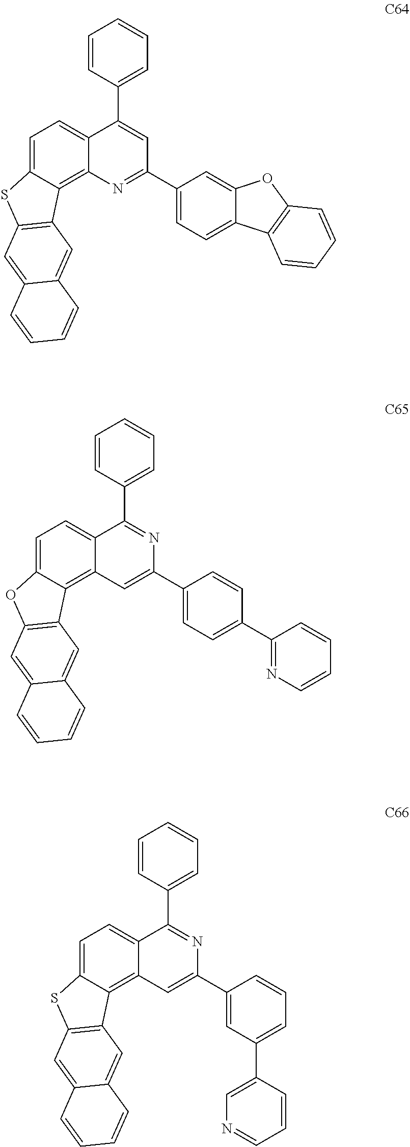


Priority Applications (2)
| Application Number | Priority Date | Filing Date | Title |
|---|---|---|---|
| US16/252,740 US11211568B2 (en) | 2019-01-21 | 2019-01-21 | Compound for organic electroluminescence device using the same |
| TW109102049A TWI766230B (en) | 2019-01-21 | 2020-01-21 | Organic compound and organic electroluminescence device using the same |
Applications Claiming Priority (1)
| Application Number | Priority Date | Filing Date | Title |
|---|---|---|---|
| US16/252,740 US11211568B2 (en) | 2019-01-21 | 2019-01-21 | Compound for organic electroluminescence device using the same |
Publications (2)
| Publication Number | Publication Date |
|---|---|
| US20200235311A1 US20200235311A1 (en) | 2020-07-23 |
| US11211568B2 true US11211568B2 (en) | 2021-12-28 |
Family
ID=71608415
Family Applications (1)
| Application Number | Title | Priority Date | Filing Date |
|---|---|---|---|
| US16/252,740 Expired - Fee Related US11211568B2 (en) | 2019-01-21 | 2019-01-21 | Compound for organic electroluminescence device using the same |
Country Status (2)
| Country | Link |
|---|---|
| US (1) | US11211568B2 (en) |
| TW (1) | TWI766230B (en) |
Citations (3)
| Publication number | Priority date | Publication date | Assignee | Title |
|---|---|---|---|---|
| US20150144898A1 (en) * | 2012-05-30 | 2015-05-28 | Guangdong Aglaia Optoelectronic Materials Co., Ltd | Organic electroluminescent device |
| KR20170139895A (en) * | 2016-06-10 | 2017-12-20 | 에스에프씨 주식회사 | Novel heterocyclic compounds and organic light-emitting diode including the same |
| US20180006242A1 (en) | 2015-05-13 | 2018-01-04 | Samsung Sdi Co., Ltd. | Compound for organic optoelectronic diode, organic optoelectronic diode comprising same, and display device |
Family Cites Families (3)
| Publication number | Priority date | Publication date | Assignee | Title |
|---|---|---|---|---|
| CN103242299A (en) * | 2013-05-16 | 2013-08-14 | 吉林大学 | Quinazoline derivative and application thereof in organic electroluminescent device |
| CN103467447B (en) * | 2013-09-04 | 2015-10-28 | 吉林奥来德光电材料股份有限公司 | One class electroluminescent organic material and applying in the devices |
| WO2018123783A1 (en) * | 2016-12-27 | 2018-07-05 | 新日鉄住金化学株式会社 | Material for organic electroluminescent element, and organic electroluminescent element |
-
2019
- 2019-01-21 US US16/252,740 patent/US11211568B2/en not_active Expired - Fee Related
-
2020
- 2020-01-21 TW TW109102049A patent/TWI766230B/en not_active IP Right Cessation
Patent Citations (3)
| Publication number | Priority date | Publication date | Assignee | Title |
|---|---|---|---|---|
| US20150144898A1 (en) * | 2012-05-30 | 2015-05-28 | Guangdong Aglaia Optoelectronic Materials Co., Ltd | Organic electroluminescent device |
| US20180006242A1 (en) | 2015-05-13 | 2018-01-04 | Samsung Sdi Co., Ltd. | Compound for organic optoelectronic diode, organic optoelectronic diode comprising same, and display device |
| KR20170139895A (en) * | 2016-06-10 | 2017-12-20 | 에스에프씨 주식회사 | Novel heterocyclic compounds and organic light-emitting diode including the same |
Non-Patent Citations (1)
| Title |
|---|
| Machine English translation of Lee et al. (KR-10-2017-0139895). Apr. 19, 2021. * |
Also Published As
| Publication number | Publication date |
|---|---|
| TW202028422A (en) | 2020-08-01 |
| TWI766230B (en) | 2022-06-01 |
| US20200235311A1 (en) | 2020-07-23 |
Similar Documents
| Publication | Publication Date | Title |
|---|---|---|
| US10886477B2 (en) | Iridium complex and organic electroluminescence device using the same | |
| US11038120B2 (en) | Organic compound and organic electroluminescence device using the same | |
| US9190619B2 (en) | Compound for organic electroluminescence device | |
| US10103339B2 (en) | Iridium complexes and organic electroluminescence device using the same | |
| US9812649B2 (en) | Indenotriphenylene-based amine derivative for organic electroluminescent device | |
| US9698351B2 (en) | Organic material for electroluminescent device | |
| US9893305B2 (en) | Indenotriphenylene-based iridium complexes for organic electroluminescence device | |
| US11239435B2 (en) | Iridium complex and organic electroluminescence device using the same | |
| US9905772B2 (en) | Material for organic electroluminescence device and use thereof | |
| US11111244B2 (en) | Organic compound and organic electroluminescence device using the same | |
| US10079347B2 (en) | Compounds for organic electroluminescence device | |
| US11236075B2 (en) | Organic compound and organic electroluminescence device using the same | |
| US10622566B2 (en) | Polyheteroaromatic compound and organic electroluminescence device using the same | |
| US10186668B2 (en) | Organic electroluminescent material and use thereof | |
| US20160380207A1 (en) | Triphenylene-based fused biscarbazole derivative and use thereof | |
| US20200235306A1 (en) | Organic compound and organic electroluminescence device using the same | |
| US20200106028A1 (en) | Iridium complex and organic electroluminescence device using the same | |
| US20180301631A1 (en) | Light emitting material for organic electroluminescence device | |
| US10844043B2 (en) | Heteroaromatic compound and organic electroluminescence device using the same | |
| US10056561B2 (en) | Organic material and organic electroluminescent device using the same | |
| US10807972B2 (en) | Indenotriphenylene-based amine derivative and organic electroluminescence device using the same | |
| US9831444B1 (en) | Phenanthroline-based compound for organic electroluminescence device | |
| US10686146B2 (en) | Paracyclophane-based iridium complexes for organic electroluminescence device | |
| US11005047B2 (en) | Heteroaromatic compound and organic electroluminescence device using the same | |
| US20190273210A1 (en) | Heteroaromatic compound and organic electroluminescence device using the same |
Legal Events
| Date | Code | Title | Description |
|---|---|---|---|
| FEPP | Fee payment procedure |
Free format text: ENTITY STATUS SET TO UNDISCOUNTED (ORIGINAL EVENT CODE: BIG.); ENTITY STATUS OF PATENT OWNER: SMALL ENTITY |
|
| FEPP | Fee payment procedure |
Free format text: ENTITY STATUS SET TO SMALL (ORIGINAL EVENT CODE: SMAL); ENTITY STATUS OF PATENT OWNER: SMALL ENTITY |
|
| AS | Assignment |
Owner name: LUMINESCENCE TECHNOLOGY CORP., TAIWAN Free format text: ASSIGNMENT OF ASSIGNORS INTEREST;ASSIGNORS:YEN, FENG-WEN;HSIAO, WEN-FENG;REEL/FRAME:053968/0270 Effective date: 20201005 |
|
| STPP | Information on status: patent application and granting procedure in general |
Free format text: NON FINAL ACTION MAILED |
|
| STPP | Information on status: patent application and granting procedure in general |
Free format text: RESPONSE TO NON-FINAL OFFICE ACTION ENTERED AND FORWARDED TO EXAMINER |
|
| STPP | Information on status: patent application and granting procedure in general |
Free format text: NOTICE OF ALLOWANCE MAILED -- APPLICATION RECEIVED IN OFFICE OF PUBLICATIONS |
|
| STPP | Information on status: patent application and granting procedure in general |
Free format text: PUBLICATIONS -- ISSUE FEE PAYMENT VERIFIED |
|
| STCF | Information on status: patent grant |
Free format text: PATENTED CASE |
|
| FEPP | Fee payment procedure |
Free format text: MAINTENANCE FEE REMINDER MAILED (ORIGINAL EVENT CODE: REM.); ENTITY STATUS OF PATENT OWNER: SMALL ENTITY |
|
| LAPS | Lapse for failure to pay maintenance fees |
Free format text: PATENT EXPIRED FOR FAILURE TO PAY MAINTENANCE FEES (ORIGINAL EVENT CODE: EXP.); ENTITY STATUS OF PATENT OWNER: SMALL ENTITY |
|
| STCH | Information on status: patent discontinuation |
Free format text: PATENT EXPIRED DUE TO NONPAYMENT OF MAINTENANCE FEES UNDER 37 CFR 1.362 |
|
| FP | Lapsed due to failure to pay maintenance fee |
Effective date: 20251228 |