US11201616B2 - Voltage tolerant interface circuit - Google Patents
Voltage tolerant interface circuit Download PDFInfo
- Publication number
- US11201616B2 US11201616B2 US17/081,888 US202017081888A US11201616B2 US 11201616 B2 US11201616 B2 US 11201616B2 US 202017081888 A US202017081888 A US 202017081888A US 11201616 B2 US11201616 B2 US 11201616B2
- Authority
- US
- United States
- Prior art keywords
- voltage
- transistor
- low
- interface circuit
- blocking
- Prior art date
- Legal status (The legal status is an assumption and is not a legal conclusion. Google has not performed a legal analysis and makes no representation as to the accuracy of the status listed.)
- Active
Links
Images


Classifications
-
- H—ELECTRICITY
- H03—ELECTRONIC CIRCUITRY
- H03K—PULSE TECHNIQUE
- H03K17/00—Electronic switching or gating, i.e. not by contact-making and –breaking
- H03K17/08—Modifications for protecting switching circuit against overcurrent or overvoltage
- H03K17/082—Modifications for protecting switching circuit against overcurrent or overvoltage by feedback from the output to the control circuit
- H03K17/0822—Modifications for protecting switching circuit against overcurrent or overvoltage by feedback from the output to the control circuit in field-effect transistor switches
-
- H—ELECTRICITY
- H03—ELECTRONIC CIRCUITRY
- H03K—PULSE TECHNIQUE
- H03K5/00—Manipulating of pulses not covered by one of the other main groups of this subclass
- H03K5/22—Circuits having more than one input and one output for comparing pulses or pulse trains with each other according to input signal characteristics, e.g. slope, integral
- H03K5/24—Circuits having more than one input and one output for comparing pulses or pulse trains with each other according to input signal characteristics, e.g. slope, integral the characteristic being amplitude
- H03K5/2472—Circuits having more than one input and one output for comparing pulses or pulse trains with each other according to input signal characteristics, e.g. slope, integral the characteristic being amplitude using field effect transistors
- H03K5/2481—Circuits having more than one input and one output for comparing pulses or pulse trains with each other according to input signal characteristics, e.g. slope, integral the characteristic being amplitude using field effect transistors with at least one differential stage
Definitions
- Low-voltage transistors can be advantageous for a wide variety of electronics applications due to their high speed, low power consumption, and small size. Despite their potential advantages, however, the use of low-voltage transistors may be limited by their susceptibility to damage or failure when exposed to the high voltages present in many applications.
- DC-DC voltage regulation One common application where high voltages are typically present is DC-DC voltage regulation. Nevertheless, high bandwidth, high accuracy, DC-DC voltage regulators require high speed circuits that low-voltage transistors are well suited to implement.
- a DC-DC voltage regulator may require a high speed comparator to sample an operating characteristic of a power transistor when it is turned on. While the power transistor is turned on, the voltages encountered in measuring its operation are typically safe for low-voltage transistors to be exposed to. However, when the power transistor is turned off, it may be at a voltage that substantially exceeds such a safe voltage level. Consequently, there is a need in the art for a solution enabling use of low-voltage transistors in applications in which voltages exceeding their voltage tolerance may be present.
- the present disclosure is directed to voltage tolerant circuits and systems, substantially as shown in and/or described in connection with at least one of the figures, and as set forth in the claims.
- FIG. 1 shows a diagram of an exemplary system-on-chip (SoC) including an integrated voltage regulator and voltage tolerant interface circuit, according to one implementation.
- SoC system-on-chip
- FIG. 2A shows a diagram of an exemplary voltage tolerant interface circuit suitable for use as part of the SoC of FIG. 1 , according to one implementation.
- FIG. 2B shows another exemplary implementation of the voltage tolerant interface circuit of FIG. 2A .
- FIG. 2C shows yet another exemplary implementation of the voltage tolerant interface circuit of FIG. 2A .
- FIG. 3A shows a diagram of an exemplary voltage tolerant interface circuit suitable for use as part of the SoC of FIG. 1 , according to another implementation.
- FIG. 3B shows another exemplary implementation of the voltage tolerant interface circuit of FIG. 3A .
- FIG. 4A shows a diagram of an exemplary voltage tolerant interface circuit suitable for use as part of the SoC of FIG. 1 , according to another implementation.
- FIG. 4B shows another exemplary implementation of the voltage tolerant interface circuit of FIG. 4A .
- FIG. 5 shows a diagram of an exemplary voltage tolerant interface circuit suitable for use as part of the SoC of FIG. 1 , according to yet another implementation.
- low-voltage transistors can be advantageous for a wide variety of electronics applications due to their high speed, low power consumption, and small size. As further stated above, despite their potential advantages, the use of low-voltage transistors may be limited by their susceptibility to damage or failure when exposed to the high voltages present in many applications, such as DC-DC voltage regulation, for example.
- the present application addresses and overcomes the constraints on the use of low-voltage transistors by disclosing a solution enabling use of low-voltage transistors in applications in which voltages exceeding their voltage tolerance may be present.
- the present inventive principles provide voltage protection for the low-voltage transistor.
- the blocking transistor protects the control terminal of the low-voltage transistor by blocking the voltage received at the input terminal when the voltage exceeds a voltage tolerance of the low-voltage transistor.
- the low-voltage transistor receives a supply voltage higher than its voltage tolerance. In that implementation, the blocking transistor protects the control terminal of the low-voltage transistor by blocking the voltage received at the input terminal when the voltage is below a predetermined threshold.
- the expression “voltage tolerance” refers to the maximum voltage that a transistor can sustain between any two terminals without being damaged.
- the voltage tolerance of the low-voltage FET is the maximum voltage the FET can sustain between any two of its gate, source, drain, and body terminals.
- a low-voltage FET is described as having a voltage tolerance of up to one volt (1.0 V)
- that FET can tolerate a voltage difference of up to a maximum of 1.0 V between any two of its gate, source, drain, and body terminals without being damaged.
- FIG. 1 shows a diagram of exemplary system-on-chip (SoC) 100 including integrated voltage regulator 106 and voltage tolerant interface circuit 110 , according to one implementation.
- SoC system-on-chip
- voltage tolerant interface circuit 110 receives an input voltage at input terminal 102 and generates output 104 based on the voltage received at input terminal 102 .
- output 104 is provided to integrated voltage regulator 106 , which processes output 104 as part of providing a regulated voltage at regulated voltage output 108 of SoC 100 .
- Integrated voltage regulator 106 may be a high bandwidth, highly accurate “on chip” DC-DC voltage regulator.
- voltage tolerant interface circuit 110 is included on chip with integrated voltage regulator 106 as part of SoC 100 . Consequently, it may be advantageous of desirable to implement voltage tolerant interface circuit 110 using low-voltage transistors to enhance its speed, reduce its power consumption, and minimize its size on chip.
- voltage tolerant interface circuit 110 may take the form of a high speed comparator including low-voltage transistors having a voltage tolerance of 1.0 V or less, such as 0.9 V, or even less.
- voltage tolerant interface circuit 110 may take the form of an amplifier or level converter, to name merely two alternative examples.
- the input voltage received by voltage tolerant interface circuit 110 at input terminal 102 may be variable, and may sometimes exceed, or substantially exceed, the voltage tolerance of the low-voltage transistors utilized in voltage tolerant interface circuit 110 .
- the input voltage at input terminal 102 may vary between zero volts (0.0 V) and 1.8 V.
- voltage tolerant input circuit 110 includes features providing voltage protection to one or more low-voltage transistors it includes.
- FIG. 2A shows a diagram of exemplary voltage tolerant interface circuit 210 A suitable for use as part of SoC 100 in FIG. 1 , according to one implementation.
- exemplary voltage tolerant interface circuit 210 A is implemented as a differential comparator receiving input voltage (V IN ) at input terminal 202 and generating output 204 at differential output terminals 204 a and 204 b based on the voltage V IN received at input terminal 202 .
- Voltage tolerant interface circuit 210 A having input terminal 202 and providing output 204 corresponds in general to voltage tolerant interface circuit 110 having input terminal 102 and providing output 104 , in FIG. 1 . Consequently, voltage tolerant interface circuits 110 and 210 A may share features and attributes that are common to both circuits.
- voltage tolerant interface circuit 210 A includes differential pair transistors 230 a and 230 b , and supply rail transistor 228 , each implemented as a low-voltage transistor having a voltage tolerance of up to approximately 1.0 V.
- voltage tolerant interface circuit 210 A includes first blocking transistor 220 a , optional second blocking transistor 220 b , low reference voltage input 214 A, and load devices 218 a and 218 b shown as respective load resistors. Also shown in FIG. 2A are low voltage supply (V DD ) 212 A and ground or V SS 216 A.
- voltage tolerant interface circuit 210 A includes differential pair transistors 230 a and 230 b , supply rail transistor 228 , first blocking transistor 220 a , and optional second blocking transistor 220 b in the form of FETs, that representation is merely exemplary.
- differential pair transistors 230 a and 230 b , supply rail transistor 228 , first blocking transistor 220 a , and optional second blocking transistor 220 b may take the form of any switching devices suitable to the purposes of voltage tolerant interface circuit 210 A and/or SoC 100 .
- each of differential pair transistors 230 a and 230 b , and supply rail transistor 228 is shown as a P type FET (PFET), while each of first blocking transistor 220 a and optional second blocking transistor 220 b takes the form of an N type FET (NFET).
- PFET P type FET
- NFET N type FET
- first blocking transistor 220 a has source 222 a , drain 224 a , and gate 226 a
- optional second blocking transistor 220 b has source 222 b , drain 224 b , and gate 226 b .
- differential pair transistor 230 a has source 232 a , drain 234 a , and gate 236 a (hereinafter “control terminal 236 a ”)
- differential pair transistor 230 b has source 232 b , drain 234 b , and gate 236 b (hereinafter “control terminal 236 b ”).
- supply rail transistor 228 is coupled between V DD 212 A and sources 232 a and 232 b of respective differential pair transistors 230 a and 230 b .
- differential output terminal 204 a is situated between drain 234 a of differential pair transistor 230 a and load device 218 a
- differential output terminal 204 b is situated between drain 234 b of differential pair transistor 230 b and load device 218 b.
- Load device 218 a couples drain 234 a of differential pair transistor 230 a to ground or V SS 216 A, while load device 218 b couples drain 234 b of differential pair transistor 230 b to ground or V SS 216 A. It is noted that although load devices 218 a and 218 b are resistors having substantially identical resistance in the implementation of FIG. 2A , that representation is merely by way of example. In other implementations, load devices 218 a and 218 b may take the form of diodes or transistors having substantially similar performance characteristics to one another.
- First blocking transistor 220 a is coupled between control terminal 236 a of low-voltage differential pair transistor 230 a and input terminal 202 . That is to say, according to the exemplary implementation shown in FIG. 2A , source 222 a of NFET first blocking transistor 220 a may be directly coupled to control terminal 236 a of PFET differential pair transistor 230 a . Moreover, drain 224 a of first blocking transistor 220 a may be directly coupled to input terminal 202 .
- optional second blocking transistor 220 b may be coupled between control terminal 236 b of low-voltage differential pair transistor 230 b and reference voltage input 214 A.
- source 222 b of NFET second blocking transistor 220 b may be directly coupled to control terminal 236 b of PFET differential pair transistor 230 b .
- drain 224 b of second blocking transistor 220 b may be directly coupled to reference voltage input 214 A.
- control terminal 236 b of low-voltage differential pair transistor 230 b may be directly coupled to reference voltage input 214 A. It is noted that inclusion or omission of second blocking transistor 220 b in voltage tolerant interface circuit 210 A is a matter of design choice.
- voltage tolerant interface circuit 210 A compares voltage V IN applied to a terminal, e.g., drain 224 a , of first blocking transistor 220 a to a reference voltage (V REF ) applied to reference voltage input 214 A.
- V REF reference voltage
- differential pair transistors 230 a and 230 b , and supply rail transistor 228 may each be a low-voltage transistor having a voltage tolerance of up to approximately 1.0 V.
- input voltage V IN at input terminal 102 / 202 of voltage tolerant interface circuit 110 / 210 A may vary between 0.0 V and 1.8 V.
- low voltage supply V DD 212 A may be at 0.9 V
- V REF applied to reference voltage input 214 A may be in a range between 0.0 V and 0.5 V, such as 0.3 V for example
- load devices 218 a and 218 b may be considered to be coupled between respective differential output terminals 204 a and 204 b and ground 216 A.
- load devices 218 a and 218 b may take the form of resistors having substantially identical resistance in a range from approximately five hundred ohms (500 ⁇ ) to approximately fifty kilo ohms (50 k ⁇ ).
- First blocking transistor 220 a and optional second blocking transistor 220 b have their respective gates 226 a and 226 b biased at a voltage between V REF and the voltage tolerance of low-voltage differential pair transistors 230 a and 230 b . As a result of that biasing, first blocking transistor 220 a and optional second blocking transistor 220 b are always-on blocking transistors.
- first blocking transistor 220 a and optional second blocking transistor 220 b are always-on, their switching speed is not relevant to the overall performance of voltage tolerant interface circuit 210 A. Consequently, first blocking transistor 220 a and optional second blocking transistor 220 b may be implemented using small, fast, low-voltage transistors or using larger, slower, higher voltage tolerant transistors. In one implementation, first blocking transistor 220 a and optional second blocking transistor 220 b may take the form of low-voltage transistors having a voltage tolerance substantially equal to the voltage tolerance of low-voltage differential pair transistors 230 a and 230 b , i.e., a voltage tolerance of up to approximately 1.0 V.
- optional second blocking transistor 220 b may be omitted and control terminal 236 b of low-voltage differential pair transistor 230 b may be directly coupled to reference voltage input 214 A.
- optional second blocking transistor 220 b may be coupled between control terminal 236 b of low-voltage differential pair transistor 230 b and reference voltage input 214 A, and may have its gate 226 b biased higher than V REF .
- V REF is equal to 0.3 V
- gate 226 b of second blocking transistor 220 b may be biased at 0.6 V.
- second blocking transistor 220 b is included in voltage tolerant interface circuit 210 A or not, a voltage approximately equal to V REF is applied to control terminal 236 b of low-voltage differential pair transistor 230 b .
- low-voltage differential pair transistor 230 b is a PFET and its gate-to-source voltage is negative, low-voltage differential pair transistor 230 b is on, resulting in current flow through load device 218 b and an output voltage at differential output terminal 204 b.
- First blocking transistor 220 a is coupled between control terminal 236 a of low-voltage differential pair transistor 230 a and input terminal 202 , and may have its gate 226 a biased higher than V REF .
- gate 226 a of first blocking transistor 220 a may be biased at 0.6 V. In that biased state, first blocking transistor 220 a will block a portion of V IN when V IN is higher than the biasing voltage applied to gate 226 a . In other words, a voltage at source 222 a of first blocking transistor 220 a will not exceed the biasing voltage applied to gate 226 a .
- first blocking transistor 220 a protects control terminal 236 a of low-voltage differential pair transistor 230 a by blocking the voltage received at input terminal 202 when V IN exceeds the voltage tolerance of low-voltage differential pair transistor 230 a.
- low-voltage differential pair transistor 230 a is a PFET and its gate-to-source voltage is negative, low-voltage differential pair transistor 230 a is also on, resulting in current flow through load device 218 a and an output voltage at differential output terminal 204 a.
- the gate-to-source voltage of low-voltage differential pair transistor 230 a is less negative than the gate-to-source voltage of low-voltage differential pair transistor 230 b as long as control terminal 236 a sees the bias voltage applied to gate 226 a of first blocking transistor 220 a , resulting in a difference between the voltages present at respective differential output terminals 204 a and 204 b.
- first blocking transistor 220 a When V IN is below the bias voltage applied to gate 226 a of first blocking transistor 220 a , first blocking transistor 220 a passes V IN to control terminal 236 a of low-voltage differential pair transistor 230 a . As long as V IN is greater than V REF , a differential voltage having a consistent polarity will be present at output 204 . However, when V IN drops below V REF , the polarity of the differential voltage at output 204 is reversed. Consequently, first blocking transistor 220 a advantageously enables use of low-voltage differential transistors 230 a and 230 b to implement voltage tolerant interface circuit 210 A as a differential comparator, while also advantageously protecting low-voltage differential pair transistor 230 a from voltages exceeding its voltage tolerance.
- Exemplary voltage tolerant interface circuit 210 A is configured to compare V IN to V REF when V IN is at the low end of its variable voltage range, i.e., between approximately 0.0 V and approximately 0.9 V. However, in some applications, it may be advantageous or desirable to utilize a voltage tolerant interface circuit including low-voltage transistors to sample compare V IN to V REF when V IN is higher, i.e., up to approximately 1.8 V.
- FIG. 2B shows one exemplary implementation of such a voltage tolerant interface circuit.
- exemplary voltage tolerant interface circuit 210 B is implemented as a differential comparator receiving V IN at input terminal 202 and generating output 204 at differential output terminals 204 a and 204 b based on V IN .
- Voltage tolerant interface circuit 210 B having input terminal 202 and providing output 204 corresponds in general to voltage tolerant interface circuit 110 having input terminal 102 and providing output 104 , in FIG. 1 . Consequently, voltage tolerant interface circuits 110 and 210 B may share any of the features attributed to either of voltage tolerant interface circuits 110 and 210 B in the present disclosure.
- voltage tolerant interface circuit 210 B shares many features in common with voltage tolerant interface circuit 210 A, in FIG. 2A . It is further noted that any features identified in FIG. 2B by reference numbers identical to those used to identify corresponding features in FIG. 2A may share any of the characteristics attributed to those corresponding features above. Thus differential pair transistors 230 a and 230 b , supply rail transistor 228 , and load devices 218 a and 218 b may have any of the characteristics described above by reference to FIG. 2A .
- voltage tolerant interface circuit 210 B includes first blocking transistor 240 a and optional second blocking transistor 240 b in the form of PFET devices, in contrast to the NFET devices utilized for first blocking transistor 220 a and optional second blocking transistor 220 b in FIG. 2A .
- voltage tolerant interface circuit 210 B includes high reference voltage input 214 B, high voltage supply V DD 212 B and ground or low voltage 216 B less than V DD .
- voltage tolerant interface circuit 210 B includes first blocking transistor 240 a and optional second blocking transistor 240 b in the form of FETs, that representation is merely exemplary. In other implementations, first blocking transistor 240 a and optional second blocking transistor 240 b may take the form of any switching devices suitable to the purposes of voltage tolerant interface circuit 210 B and/or SoC 100 .
- differential pair transistors 230 a and 230 b , and supply rail transistor 228 may each be a low-voltage transistor having a voltage tolerance of up to approximately 1.0 V.
- input voltage V IN at input terminal 102 / 202 of voltage tolerant interface circuit 110 / 210 A may vary between 0.0 V and 1.8 V.
- high voltage supply V DD 212 B may be at 1.8 V. That is to say, low-voltage differential pair transistors 230 a and 230 b , and supply rail transistor 228 , receive supply voltage V DD 212 B that may be higher than the voltage tolerance of those low-voltage transistors.
- V REF applied to reference voltage input 214 B may be in a range between 1.3 V and 1.8 V, such as 1.5 V for example, and load devices 218 a and 218 b may be considered to be coupled between respective differential output terminals 204 a and 204 b and low voltage 216 B at approximately 0.9 V.
- low-voltage differential pair transistors 230 a and 230 b , and low-voltage supply rail transistor 228 are exposed to supply voltage V DD 212 B higher than their voltage tolerance, those devices can operate safely as long as the voltage across any two terminals remains within their voltage tolerance.
- voltage tolerant interface circuit 210 B can safely compare V IN between 0.9 V and 1.8 V with V REF in that range.
- the body terminals of each of low-voltage differential pair transistors 230 a and 230 b , and low-voltage supply rail transistor 228 may be tied to their respective sources.
- first blocking transistor 240 a includes source 242 a , drain 244 a , and gate 246 a
- optional second blocking transistor 240 b includes source 242 b , drain 244 b , and gate 246 b
- first blocking transistor 240 a is coupled between control terminal 236 a of low-voltage differential pair transistor 230 a and input terminal 202 . That is to say, according to the exemplary implementation shown in FIG. 2B , drain 244 a of PFET first blocking transistor 240 a may be directly coupled to control terminal 236 a of PFET differential pair transistor 230 a . Moreover, source 242 a of first blocking transistor 240 a may be directly coupled to input terminal 202 .
- optional second blocking transistor 240 b may be coupled between control terminal 236 b of low-voltage differential pair transistor 230 b and reference voltage input 214 B.
- drain 244 b of PFET second blocking transistor 240 b may be directly coupled to control terminal 236 b of PFET differential pair transistor 230 b .
- source 242 b of second blocking transistor 240 b may be directly coupled to reference voltage input 214 B.
- control terminal 236 b of low-voltage differential pair transistor 230 b may be directly coupled to reference voltage input 214 B. It is noted that inclusion or omission of second blocking transistor 240 b in voltage tolerant interface circuit 210 B is a matter of design choice.
- voltage tolerant interface circuit 210 B compares voltage V IN applied to a terminal, e.g., source 242 a , of first blocking transistor 240 a to reference voltage V REF applied to reference voltage input 214 B.
- First blocking transistor 240 a and optional second blocking transistor 240 b have their respective gates 246 a and 246 b biased at a voltage below V REF and above the difference between high voltage supply V DD 212 B and the voltage tolerance of low-voltage differential pair transistors 230 a and 230 b .
- first blocking transistor 240 a and optional second blocking transistor 240 b are always-on blocking transistors.
- first blocking transistor 240 a and optional second blocking transistor 240 b are always-on, their switching speed is not relevant to the overall performance of voltage tolerant interface circuit 210 B. Consequently, first blocking transistor 240 a and optional second blocking transistor 240 b may be implemented using small, fast, low-voltage transistors or using larger, slower, higher voltage tolerant transistors. In one implementation, first blocking transistor 240 a and optional second blocking transistor 240 b may take the form of low-voltage transistors having a voltage tolerance substantially equal to the voltage tolerance of low-voltage differential pair transistors 230 a and 230 b , i.e., a voltage tolerance of up to approximately 1.0 V.
- optional second blocking transistor 240 b may be omitted and control terminal 236 b of low-voltage differential pair transistor 230 b may be directly coupled to reference voltage input 214 B.
- optional second blocking transistor 240 b may be coupled between control terminal 236 b of low-voltage differential pair transistor 230 b and reference voltage input 214 B, and may have its gate 246 b biased lower than V REF .
- V REF is equal to 1.5 V
- gate 246 b of second blocking transistor 240 b may be biased at 1.3 V.
- second blocking transistor 240 b is included in voltage tolerant interface circuit 210 B or not, a voltage approximately equal to V REF is applied to control terminal 246 b of low-voltage differential pair transistor 230 b .
- low-voltage differential pair transistor 230 b is a PFET and its gate-to-source voltage is negative, low-voltage differential pair transistor 230 b is on, resulting in current flow through load device 218 b and an output voltage at differential output terminal 204 b.
- First blocking transistor 240 a is coupled between control terminal 236 a of low-voltage differential pair transistor 230 a and input terminal 202 , and may have its gate 246 a biased lower than V REF .
- gate or 246 a of first blocking transistor 240 a may be biased at 1.3V. In that biased state, first blocking transistor 240 a will block V IN when V IN is lower than the biasing voltage applied to gate 246 a , e.g., 1.3 V. In other words, a voltage at drain 244 a of first blocking transistor 240 a will not fall significantly below the biasing voltage applied to gate 246 a .
- first blocking transistor 240 a protects control terminal 236 a of low-voltage differential pair transistor 230 a by blocking V IN received at input terminal 202 when the difference between V DD 212 B and V IN exceeds the voltage tolerance of low-voltage differential pair transistor 230 a.
- low-voltage differential pair transistor 230 a is a PFET and its gate-to-source voltage is negative, low-voltage differential pair transistor 230 a is also on, resulting in current flow through load device 218 a and an output voltage at differential output terminal 204 a.
- the gate-to-source voltage of low-voltage differential pair transistor 230 a is more negative than the gate-to-source voltage of low-voltage differential pair transistor 230 b as long as control terminal 236 a sees the bias voltage applied to gate 246 a of first blocking transistor 240 a , resulting in a difference between the voltages present at respective differential output terminals 204 a and 204 b.
- first blocking transistor 240 a When V IN is above the bias voltage applied to gate 246 a of first blocking transistor 240 a , first blocking transistor 240 a passes V IN to control terminal 236 a of low-voltage differential pair transistor 230 a . As long as V IN is less than V REF , a differential voltage having a consistent polarity will be present at output 204 . However, when V IN exceeds V REF , the polarity of the differential voltage at output 204 is reversed.
- first blocking transistor 240 a advantageously enables use of low-voltage differential transistors 230 a and 230 b to implement voltage tolerant interface circuit 210 B as a differential comparator, while also advantageously protecting low-voltage differential pair transistor 230 a from voltages below a predetermined voltage threshold.
- FIG. 2C shows another exemplary implementation of the voltage tolerant interface circuit of FIG. 2A .
- exemplary voltage tolerant interface circuit 210 C is implemented as a differential comparator receiving V IN at input terminal 202 and generating output 204 at differential output terminals 204 a and 204 b based on V IN .
- Voltage tolerant interface circuit 210 C having input terminal 202 and providing output 204 corresponds in general to voltage tolerant interface circuit 110 having input terminal 102 and providing output 104 , in FIG. 1 . Consequently, voltage tolerant interface circuits 110 and 210 C may share any of the features attributed to either of voltage tolerant interface circuits 110 and 210 C in the present disclosure.
- voltage tolerant interface circuit 210 C shares many features in common with voltage tolerant interface circuit 210 A, in FIG. 2A . It is further noted that any features identified in FIG. 2C by reference numbers identical to those used to identify corresponding features in FIG. 2A may share any of the characteristics attributed to those corresponding features above. Thus first blocking transistor 220 a , optional second blocking transistor 220 b , load devices 218 a and 218 b , low voltage supply V DD 212 A and ground or V SS 216 A may have any of the characteristics described above by reference to FIG. 2A .
- voltage tolerant interface circuit 210 B includes differential pair transistors 280 a and 280 b , and ground rail transistor 288 in the form of NFET devices, in contrast to the PFET devices utilized for differential pair transistors 230 a and 230 b , and supply rail transistor 228 in FIG. 2A .
- Differential pair transistors 280 a and 280 b , and ground rail transistor 288 may each be implemented as a low-voltage transistor having a voltage tolerance of up to approximately 1.0 V.
- voltage tolerant interface circuit 210 C includes differential pair transistors 280 a and 280 b , and ground rail transistor 288 in the form of low-voltage FETs, that representation is merely exemplary.
- differential pair transistors 280 a and 280 b , and ground rail transistor 288 may take the form of any low-voltage switching devices suitable to the purposes of voltage tolerant interface circuit 210 C and/or SoC 100 .
- each of differential pair transistors 280 a and 280 b , ground rail transistor 288 , first blocking transistor 220 a , and optional second blocking transistor 220 b takes the form of an NFET.
- differential pair transistor 280 a has source 282 a , drain 284 a , and gate 286 a (hereinafter “control terminal 286 a ”)
- differential pair transistor 280 b has source 282 b , drain 284 b , and gate 286 b (hereinafter “control terminal 286 b ”).
- ground rail transistor 288 is coupled between ground or V SS 216 A and sources 282 a and 282 b of respective differential pair transistors 280 a and 280 b .
- differential output terminal 204 a is situated to between drain 284 a of differential pair transistor 280 a and load device 218 a
- differential output terminal 204 b is situated between drain 284 b of differential pair transistor 280 b and load device 218 b.
- Load device 218 a couples drain 284 a of differential pair transistor 280 a to V DD 212 A, while load device 218 b couples drain 284 b of differential pair transistor 280 b to V DD 212 A.
- First blocking transistor 220 a is coupled between control terminal 286 a of low-voltage differential pair transistor 280 a and input terminal 202 . That is to say, according to the exemplary implementation shown in FIG. 2C , source 222 a of NFET first blocking transistor 220 a may be directly coupled to control terminal 286 a of NFET differential pair transistor 280 a . Moreover, drain 224 a of first blocking transistor 220 a may be directly coupled to input terminal 202 .
- optional second blocking transistor 220 b may be coupled between control terminal 286 b of low-voltage differential pair transistor 280 b and reference voltage input 214 A.
- source 222 b of NFET second blocking transistor 220 b may be directly coupled to control terminal 286 b of NFET differential pair transistor 280 b .
- drain 224 b of second blocking transistor 220 b may be directly coupled to reference voltage input 214 A.
- control terminal 286 b of low-voltage differential pair transistor 280 b may be directly coupled to reference voltage input 214 A. It is noted that inclusion or omission of second blocking transistor 220 b in voltage tolerant interface circuit 210 C is a matter of design choice.
- voltage tolerant interface circuit 210 C compares voltage V IN applied to a terminal, e.g., drain 224 a , of first blocking transistor 220 a to reference voltage V REF applied to reference voltage input 214 A.
- a terminal e.g., drain 224 a
- V REF reference voltage
- voltage tolerant interface circuit 210 C compares voltage V IN applied to a terminal, e.g., drain 224 a , of first blocking transistor 220 a to reference voltage V REF applied to reference voltage input 214 A.
- differential pair transistors 280 a and 280 b , and ground rail transistor 288 may each be a low-voltage transistor having a voltage tolerance of up to approximately 1.0 V.
- input voltage V IN at input terminal 102 / 202 of voltage tolerant interface circuit 110 / 210 A may vary between 0.0 V and 1.8 V.
- low voltage supply V DD 212 A may be at 0.9 V
- V REF applied to reference voltage input 214 A may be in a range between 0.0 V and 0.5 V, such as 0.3 V for example
- ground rail transistor 288 may be considered to be coupled between differential pair transistors 280 a and 280 b and ground 216 A.
- First blocking transistor 220 a and optional second blocking transistor 220 b have their respective gates 226 a and 226 b biased at a voltage between V REF and the voltage tolerance of low-voltage differential pair transistors 280 a and 280 b . As a result of that biasing, first blocking transistor 220 a and optional second blocking transistor 220 b are always-on blocking transistors.
- first blocking transistor 220 a and optional second blocking transistor 220 b are always-on, their switching speed is not relevant to the overall performance of voltage tolerant interface circuit 210 A. Consequently, first blocking transistor 220 a and optional second blocking transistor 220 b may be implemented using small, fast, low-voltage transistors or using larger, slower, higher voltage tolerant transistors. In one implementation, first blocking transistor 220 a and optional second blocking transistor 220 b may take the form of low-voltage transistors having a voltage tolerance substantially equal to the voltage tolerance of low-voltage differential pair transistors 280 a and 280 b , i.e., a voltage tolerance of up to approximately 1.0 V.
- second blocking transistor 220 b is included in voltage tolerant interface circuit 210 C or not, a voltage approximately equal to V REF is applied to control terminal 286 b of low-voltage differential pair transistor 280 b .
- low-voltage differential pair transistor 280 b is an NFET and its gate-to-source voltage is positive, low-voltage differential pair transistor 280 b is on, resulting in current flow through load device 218 b and an output voltage at differential output terminal 204 b.
- First blocking transistor 220 a is coupled between control terminal 286 a of low-voltage differential pair transistor 280 a and input terminal 202 , and may have its gate 226 a biased higher than V REF .
- gate 226 a of first blocking transistor 220 a may be biased at 0.6 V. In that biased state, first blocking transistor 220 a will block a portion of V IN when V IN is higher than the biasing voltage applied to gate 226 a . In other words, a voltage at source 222 a of first blocking transistor 220 a will not exceed the biasing voltage applied to gate 226 a .
- first blocking transistor 220 a protects control terminal 286 a of low-voltage differential pair transistor 280 a by blocking the voltage received at input terminal 202 when V IN exceeds the voltage tolerance of low-voltage differential pair transistor 280 a.
- low-voltage differential pair transistor 280 a is an NFET and its gate-to-source voltage is positive, low-voltage differential pair transistor 280 a is also on, resulting in current flow through load device 218 a and an output voltage at differential output terminal 204 a.
- the gate-to-source voltage of low-voltage differential pair transistor 280 b is less positive than the gate-to-source voltage of low-voltage differential pair transistor 280 a as long as control terminal 286 a sees the bias voltage applied to gate 226 a of first blocking transistor 220 a , resulting in a difference between the voltages present at respective differential output terminals 204 a and 204 b.
- first blocking transistor 220 a When V IN is below the bias voltage applied to gate 226 a of first blocking transistor 220 a , first blocking transistor 220 a passes V IN to control terminal 286 a of low-voltage differential pair transistor 280 a . As long as V IN is greater than V REF , a differential voltage having a consistent polarity will be present at output 204 . However, when V IN drops below V REF , the polarity of the differential voltage at output 204 is reversed. Consequently, first blocking transistor 220 a advantageously enables use of low-voltage differential transistors 280 a and 280 b to implement voltage tolerant interface circuit 210 C as a differential comparator, while also advantageously protecting low-voltage differential pair transistor 280 a from voltages exceeding its voltage tolerance.
- FIG. 3A shows a diagram of exemplary voltage tolerant interface circuit 310 A suitable for use as part of SoC 100 in FIG. 1 , according to another implementation.
- exemplary voltage tolerant interface circuit 310 A is implemented as an offset-calibrated differential comparator receiving input voltage V IN at input terminal 302 and generating output 304 at differential output terminals 304 a and 304 b based on the voltage V IN received at input terminal 302 .
- Voltage tolerant interface circuit 310 A having input terminal 302 and providing output 304 corresponds in general to voltage tolerant interface circuit 110 having input terminal 102 and providing output 104 , in FIG. 1 . Consequently, voltage tolerant interface circuits 110 and 310 A may share any of the features attributed to either of voltage tolerant interface circuits 110 and 310 A in the present disclosure.
- voltage tolerant interface circuit 310 A shares many features in common with voltage tolerant interface circuit 210 A, in FIG. 2A . It is further noted that any features identified in FIG. 2B by reference numbers corresponding to those used to identify features in FIG. 2A may share any of the characteristics attributed to those corresponding features above.
- first blocking transistor 320 a , optional second blocking transistor 320 b , and differential pair transistors 330 a and 330 b may share any of the characteristics attributed to respectively corresponding first blocking transistor 220 a , optional second blocking transistor 220 b , and differential pair transistors 230 a and 230 b , above.
- supply rail transistor 328 , load devices 318 a and 318 b , V DD 312 A, V REF at reference voltage input 314 A, and ground or V SS 316 A may share any of the characteristics attributed to respectively corresponding supply rail transistor 228 , load devices 218 a and 218 b , V DD 212 A, V REF at reference voltage input 214 A and ground or V SS 216 A, above.
- voltage tolerant interface circuit 310 A includes Phase 1 reference voltage input terminal 362 A, Phase 1 coupling transistors 350 a and 350 b , offset-calibration transistors 352 a and 352 b , offset-calibration capacitors 338 a and 338 b , and Phase 2 coupling transistors 360 a and 360 b .
- Phase 1 coupling transistors 350 a and 350 b , offset-calibration transistors 352 a and 352 b , and Phase 2 coupling transistors 360 a and 360 b may each be implemented as a low-voltage transistor having a voltage tolerance of up to approximately 1.0 V.
- offset-calibration capacitors 338 a and 338 b may each have a capacitance in a range from approximately 50 femto farads (50 fF) to approximately 200 fF.
- voltage tolerant interface circuit 310 A includes differential pair transistors 330 a and 330 b , supply rail transistor 328 , first blocking transistor 320 a , and optional second blocking transistor 320 b in the form of FETs, that representation is merely exemplary.
- the representation in FIG. 3A of Phase 1 coupling transistors 350 a and 350 b , offset-calibration transistors 352 a and 352 b , and Phase 2 coupling transistors 360 a and 360 b as FETs is also merely exemplary.
- the transistors used to implement voltage tolerant interface circuit 310 A may take the form of any switching devices suitable to the purposes of voltage tolerant interface circuit 310 A and/or SoC 100 .
- each of differential pair transistors 330 a and 330 b , and supply rail transistor 328 is shown as a PFET.
- each of first blocking transistor 320 a , optional second blocking transistor 320 b , Phase 1 coupling transistors 350 a and 350 b , offset-calibration transistors 352 a and 352 b , and Phase 2 coupling transistors 360 a and 360 b takes the form of an NFET.
- first blocking transistor 320 a has source 322 a , drain 324 a , and gate 326 a
- optional second blocking transistor 320 b has source 322 b , drain 324 b , and gate 326 b .
- differential pair transistor 330 a has source 332 a , drain 334 a , and gate 336 a (hereinafter “control terminal 336 a ”)
- differential pair transistor 330 b has source 332 b , drain 334 b , and gate 336 b (hereinafter “control terminal 336 b ”).
- First blocking transistor 320 a is coupled between control terminal 336 a of low-voltage differential pair transistor 330 a and input terminal 302 .
- source 322 a of NFET first blocking transistor 320 a may be coupled to control terminal 336 a of PFET differential pair transistor 330 a by Phase 2 coupling transistor 360 a and offset-calibration capacitor 338 a .
- drain 324 a of first blocking transistor 320 a may be directly coupled to input terminal 302 .
- optional second blocking transistor 320 b may be coupled between control terminal 336 b of low-voltage differential pair transistor 330 b and reference voltage input 314 A.
- source 322 b of NFET second blocking transistor 320 b may be coupled to control terminal 336 b of PFET differential pair transistor 330 b by Phase 2 coupling transistor 360 b and offset-calibration capacitor 338 b .
- drain 324 b of second blocking transistor 320 b may be directly coupled to reference voltage input 314 A.
- control terminal 336 b of low-voltage differential pair transistor 330 b may be coupled to reference voltage input 314 A by Phase 2 coupling transistor 360 b and offset-calibration capacitor 338 b alone. It is noted that inclusion or omission of second blocking transistor 320 b in voltage tolerant interface circuit 310 A is a matter of design choice.
- voltage tolerant interface circuit 310 A has two phases of operation.
- Phase 1 Phase 1 coupling transistors 350 a and 350 b , and offset-calibration transistors 352 a and 352 b are turned on, while Phase 2 coupling transistors 360 a and 360 b are held off.
- Phase 1 V REF is applied to control terminal 336 a of low-voltage differential pair transistor 330 a , as well as to control terminal 336 b of low-voltage differential pair transistor 330 b .
- control terminal 336 a and drain 334 a (input and output) of low-voltage differential pair transistor 330 a are shorted together, and control terminal 336 b and drain 334 b (input and output) of low-voltage differential pair transistor 330 b are shorted together, to bias voltage tolerant interface circuit 310 A at its highest gain point.
- Phase 1 operation of voltage tolerant interface circuit 310 A causes the device mismatch, or offset, of low-voltage differential pair transistors 330 a and 330 b to be stored on offset-calibration capacitors 338 a and 338 b . Consequently, during Phase 2 operation, voltage tolerant interface circuit 310 A advantageously performs as though low-voltage differential pair transistors 330 a and 330 b are matched.
- Phase 2 coupling transistors 350 a and 350 b , and offset-calibration transistors 352 a and 352 b are switched off, while Phase 2 coupling transistors 360 a and 360 b are switched on.
- the operation of voltage tolerant interface circuit 310 A is analogous to the operation of voltage tolerant interface circuit 210 A described by reference to FIG. 2A . That is to say, voltage tolerant interface circuit 310 A compares voltage V IN applied to a terminal, e.g., drain 324 a , of first blocking transistor 320 a to a reference voltage V REF applied to reference voltage input 314 A.
- control terminal 336 a is not exposed to a DC current.
- offset-calibration capacitor 338 b being interposed between control terminal 336 b of low-voltage differential pair transistor 330 b and reference voltage input 314 A, control terminal 336 b is also not exposed to a DC current.
- First blocking transistor 320 a and optional second blocking transistor 320 b have their respective gates 326 a and 326 b biased at a voltage between V REF and the voltage tolerance of low-voltage differential pair transistors 330 a and 330 b .
- first blocking transistor 320 a and optional second blocking transistor 320 b are always-on blocking transistors, i.e., during both Phase 1 operation and Phase 2 operation of voltage tolerant interface circuit 310 A.
- V REF applied to Phase 1 reference voltage input 362 A and reference voltage input 314 A is equal to 0.3 V
- gates 326 a and 326 b of first and second blocking transistor 320 a and 320 b may be biased at 0.6 V.
- second blocking transistor 320 b is included in voltage tolerant interface circuit 310 A or not, during Phase 2 operation, V REF is passed by Phase 2 coupling transistor 360 b and a voltage approximately equal to V REF corrected by the offset stored on offset-calibration capacitor 338 b is applied to control terminal 336 b of low-voltage differential pair transistor 330 b .
- low-voltage differential pair transistor 330 b is a PFET and its gate-to-source voltage is negative, low-voltage differential pair transistor 330 b is on, resulting in current flow through load device 318 b and an output voltage at differential output terminal 304 b.
- First blocking transistor 320 a is coupled between control terminal 236 a of low-voltage differential pair transistor 330 a and input terminal 302 , and may have its gate 326 a biased higher than V REF .
- V REF is equal to 0.3 V
- gate 326 a of first blocking transistor 320 a may be biased at 0.6 V. In that biased state, first blocking transistor 320 a will block a portion of V IN when V IN is higher than the biasing voltage applied to gate 326 a . In other words, a voltage at source 322 a of first blocking transistor 320 a will not exceed the biasing voltage applied to gate 326 a .
- first blocking transistor 320 a protects Phase 2 coupling transistor 360 a and control terminal 336 a of low-voltage differential pair transistor 330 a by blocking the voltage received at input terminal 302 when V IN exceeds the voltage tolerance of low-voltage differential pair transistor 330 a.
- low-voltage differential pair transistor 330 a is a PFET and its gate-to-source voltage is negative, low-voltage differential pair transistor 330 a is also on, resulting in current flow through load device 318 a and an output voltage at differential output terminal 304 a.
- the gate-to-source voltage of low-voltage differential pair transistor 330 a is less negative than the gate-to-source voltage of low-voltage differential pair transistor 330 b as long as V IN is greater than V REF , resulting in a difference between the voltages present at respective differential output terminals 304 a and 304 b .
- V IN greater than V REF
- a differential voltage having a consistent polarity will be present at output 304 .
- V IN drops below V REF
- the polarity of the differential voltage at output 304 is reversed.
- first blocking transistor 320 a advantageously enables use of low-voltage differential transistors 330 a and 330 b to implement voltage tolerant interface circuit 310 A as an offset-calibrated differential comparator, while also advantageously protecting low-voltage differential pair transistor 330 a from voltages exceeding its voltage tolerance.
- voltage tolerant interface circuit 310 A in FIG. 3A , is configured to compare V IN to V REF when V IN is at the low end of its variable voltage range, i.e., between approximately 0.0 V and approximately 0.9 V.
- V IN variable voltage range
- FIG. 3B shows one exemplary implementation of such a voltage tolerant interface circuit.
- exemplary voltage tolerant interface circuit 310 B is implemented as an offset-calibrated differential comparator receiving V IN at input terminal 302 and generating output 304 at differential output terminals 304 a and 304 b based on V IN .
- Voltage tolerant interface circuit 310 B having input terminal 302 and providing output 304 corresponds in general to voltage tolerant interface circuit 110 having input terminal 102 and providing output 104 , in FIG. 1 . Consequently, voltage tolerant interface circuits 110 and 310 B may share any of the features attributed to either of voltage tolerant interface circuits 110 and 310 B in the present disclosure.
- voltage tolerant interface circuit 310 B shares many features in common with voltage tolerant interface circuit 310 A, in FIG. 3A . It is further noted that any features identified in FIG. 3B by reference numbers identical to those used to identify corresponding features in FIG. 3A may share any of the characteristics attributed to those corresponding features above. Thus differential pair transistors 330 a and 330 b , supply rail transistor 328 , and load devices 318 a and 318 b may have any of the characteristics described above by reference to FIG. 3A .
- voltage tolerant interface circuit 310 B includes Phase 1 coupling transistors 354 a and 354 b , Phase 2 coupling transistors 364 a and 364 b , first blocking transistor 340 a , and optional second blocking transistor 340 b in the form of PFET devices, in contrast to the NFET devices utilized for Phase 1 coupling transistors 350 a and 350 b , Phase 2 coupling transistors 360 a and 360 b , first blocking transistor 320 a , and optional second blocking transistor 320 b in FIG. 3A .
- voltage tolerant interface circuit 310 B includes high voltage Phase 1 reference voltage input 362 B, high reference voltage input 314 B, high voltage supply V DD 312 B and ground or low voltage 316 B less than V DD .
- voltage tolerant interface circuit 310 B includes Phase 1 coupling transistors 354 a and 354 b , Phase 2 coupling transistors 364 a and 364 b , first blocking transistor 340 a , and optional second blocking transistor 340 b in the form of FETs, that representation is merely exemplary.
- Phase 1 coupling transistors 354 a and 354 b , Phase 2 coupling transistors 364 a and 364 b , first blocking transistor 340 a , and optional second blocking transistor 340 b may take the form of any switching devices suitable to the purposes of voltage tolerant interface circuit 310 B and/or SoC 100 .
- differential pair transistors 330 a and 330 b , and supply rail transistor 328 may each be a low-voltage transistor having a voltage tolerance of up to approximately 1.0 V.
- input voltage V IN at input terminal 102 / 302 of voltage tolerant interface circuit 110 / 310 A may vary between 0.0 V and 1.8 V.
- high voltage supply V DD 312 B may be at 1.8 V. That is to say, in some implementations, low-voltage differential pair transistors 330 a and 330 b , and supply rail transistor 328 , may receive supply voltage V DD 312 B that is higher than the voltage tolerance of those low-voltage transistors.
- V REF applied to Phase 1 reference voltage input 362 B and reference voltage input 314 B may be in a range between 1.3 V and 1.8 V, such as 1.5 V for example, while load devices 318 a and 318 b may be considered to be coupled between respective differential output terminals 304 a and 304 b and low voltage 316 B at approximately 0.9 V.
- low-voltage differential pair transistors 330 a and 330 b are exposed to supply voltage V DD 312 B higher than their voltage tolerance, those devices can operate safely as long as the voltage across any two terminals remains within their voltage tolerance.
- voltage tolerant interface circuit 310 B can safely compare V IN between 0.9 V and 1.8 V with V REF in that range.
- the body terminals of each the low-voltage transistors used in voltage tolerant interface circuit 310 B may be tied to their respective sources.
- voltage tolerant interface circuit 310 B has two phases of operation.
- Phase 1 Phase 1 coupling transistors 354 a and 354 b , and offset-calibration transistors 352 a and 352 b are turned on, while Phase 2 coupling transistors 364 a and 364 b are held off.
- Phase 1 Phase 1 coupling transistors 354 a and 354 b , and offset-calibration transistors 352 a and 352 b are turned on, while Phase 2 coupling transistors 364 a and 364 b are held off.
- V REF is applied to control terminal 336 a of low-voltage differential pair transistor 330 a , as well as to control terminal 336 b of low-voltage differential pair transistor 330 b .
- control terminal 336 a and drain 334 a of low-voltage differential pair transistor 330 a are shorted together, and control terminal 336 b and drain 334 b of low-voltage differential pair transistor 330 b are shorted together, to bias voltage tolerant interface circuit 310 B at its highest gain point.
- Phase 1 operation of voltage tolerant interface circuit 310 A causes the device mismatch, or offset, of low-voltage differential pair transistors 330 a and 330 b to be stored on offset-calibration capacitors 338 a and 338 b . Consequently, during Phase 2 operation, voltage tolerant interface circuit 310 B advantageously performs as though low-voltage differential pair transistors 330 a and 330 b are matched.
- Phase 2 Phase 1 coupling transistors 354 a and 354 b , and offset-calibration transistors 352 a and 352 b are switched off, while Phase 2 coupling transistors 364 a and 364 b are switched on.
- the operation of voltage tolerant interface circuit 310 B is analogous to the operation of voltage tolerant interface circuit 210 B described by reference to FIG. 2B . That is to say, voltage tolerant interface circuit 310 B compares voltage V IN applied to a terminal, e.g., source 342 a , of first blocking transistor 340 a to a reference voltage V REF applied to reference voltage input 314 B.
- control terminal 336 a is not exposed to a DC current.
- offset-calibration capacitor 338 b being interposed between control terminal 336 b of low-voltage differential pair transistor 330 b and reference voltage input 314 B, control terminal 336 b is also not exposed to a DC current.
- First blocking transistor 340 a and optional second blocking transistor 340 b have their respective gates 346 a and 346 b biased at a voltage below V REF and above the difference between high voltage supply V DD 312 B and the voltage tolerance of the low-voltage transistors utilized in voltage tolerant interface circuit 310 B. As a result of that biasing, first blocking transistor 340 a and optional second blocking transistor 340 b are always-on blocking transistors, i.e., during both Phase 1 operation and Phase 2 operation of voltage tolerant interface circuit 310 B.
- gates 346 a and 346 b of first and second blocking transistors 320 a and 320 b may be biased at 1.3 V.
- second blocking transistor 340 b is included in voltage tolerant interface circuit 310 B or not, during Phase 2 operation, V REF is passed by Phase 2 coupling transistor 364 b and a voltage approximately equal to V REF corrected by the offset stored on offset-calibration capacitor 338 b is applied to control terminal 336 b of low-voltage differential pair transistor 330 b .
- low-voltage differential pair transistor 330 b is a PFET and its gate-to-source voltage is negative, low-voltage differential pair transistor 330 b is on, resulting in current flow through load device 318 b and an output voltage at differential output terminal 304 b.
- First blocking transistor 340 a is coupled between control terminal 336 a of low-voltage differential pair transistor 330 a and input terminal 302 , and may have its gate 346 a biased lower than V REF .
- gate 346 a of first blocking transistor 340 a may be biased at 1.3 V. In that biased state, first blocking transistor 340 a will block V IN when V IN is lower than the biasing voltage applied to gate 346 a , e.g., 1.3 V. In other words, a voltage at drain 344 a of first blocking transistor 340 a will not exceed the biasing voltage applied to gate 346 a .
- first blocking transistor 340 a protects Phase 2 coupling transistor 364 a and control terminal 336 a of low-voltage differential pair transistor 330 a by blocking the voltage received at input terminal 302 when the difference between V DD 312 B and V IN exceeds the voltage tolerance of low-voltage differential pair transistor 330 a.
- low-voltage differential pair transistor 330 a is a PFET and its gate-to-source voltage is negative, low-voltage differential pair transistor 330 a is also on, resulting in current flow through load device 318 a and an output voltage at differential output terminal 304 a.
- the gate-to-source voltage of low-voltage differential pair transistor 330 a is more negative than the gate-to-source voltage of low-voltage differential pair transistor 330 b as long as V IN is less than V REF , resulting in a difference between the voltages present at respective differential output terminals 304 a and 304 b .
- V IN less than V REF
- a differential voltage having a consistent polarity will be present at output 304 .
- V IN exceeds V REF
- the polarity of the differential voltage at output 304 is reversed.
- first blocking transistor 340 a advantageously enables use of low-voltage differential transistors 330 a and 330 b to implement voltage tolerant interface circuit 310 B as an offset-calibrated differential comparator, while also advantageously protecting low-voltage differential pair transistor 330 a from voltages below a predetermined threshold voltage.
- FIG. 4A shows a diagram of exemplary voltage tolerant interface circuit 410 A suitable for use as part of SoC 100 in FIG. 1 , according to another implementation.
- exemplary voltage tolerant interface circuit 410 A is implemented as an offset-calibrated single-ended comparator receiving input voltage V IN at input terminal 402 and generating output 404 based on the voltage V IN received at input terminal 402 .
- Voltage tolerant interface circuit 410 A having input terminal 402 and providing output 404 corresponds in general to voltage tolerant interface circuit 110 having input terminal 102 and providing output 104 , in FIG. 1 . Consequently, voltage tolerant interface circuits 110 and 410 A may share any of the features attributed to either of voltage tolerant interface circuits 110 and 410 A in the present disclosure.
- Voltage tolerant interface circuit 410 A includes inverters 480 a and 480 b , each coupled between low voltage supply V DD 412 and V SS or ground 416 .
- Inverter 480 a includes P type transistor 482 a having control terminal 484 a , and N type transistor 486 a having control terminal 488 a .
- inverter 480 b includes P type transistor 482 b having control terminal 484 b , and N type transistor 486 b having control terminal 488 b .
- voltage tolerant interface circuit 410 A includes reference capacitor 448 , offset-calibration capacitor 468 , as well as N type Phase 1 coupling transistor 450 , N type Phase 2 coupling transistor 460 , and N type blocking transistor 420 .
- Also shown in FIG. 4A are low reference voltage input 414 A receiving V REF , Phase 1 switches 466 a and 466 b , and nodes 472 a , 474 a , 472 b , and 474
- each of inverters 480 a and 480 b , Phase 1 coupling transistor 450 , and Phase two coupling transistor 460 may be a low-voltage transistor having a voltage tolerance of up to approximately 1.0 V.
- reference capacitor 448 and offset-calibration capacitor 468 may each have a capacitance in a range from approximately 50 fF to approximately 200 fF.
- low voltage supply V DD 412 may be at 0.9 V
- V REF applied to reference voltage input 414 A may be in a range between 0.0 V and 0.5 V, such as 0.3 V for example
- inverters 480 a and 480 b may be considered to be coupled between V DD 412 and ground 416 .
- voltage tolerant interface circuit 410 A includes blocking transistor 420 , Phase 1 coupling transistor 450 , Phase two coupling transistor 460 , and inverter transistors 482 a , 486 a , 482 b , and 486 b in the form of FETs, that representation is merely exemplary.
- blocking transistor 420 , Phase 1 coupling transistor 450 , Phase two coupling transistor 460 , and inverter transistors 482 a , 486 a , 482 b , and 486 b may take the form of any switching devices suitable to the purposes of voltage tolerant interface circuit 410 A and/or SoC 100 .
- inverter transistors 482 a and 482 b are shown as PFETs, while each of blocking transistor 420 , Phase 1 coupling transistor 450 , Phase two coupling transistor 460 , and inverter transistors 486 a and 486 b takes the form of an NFET.
- blocking transistor 420 has source 422 , drain 424 , and gate 426 .
- inverter transistor 482 a is shown to have gate 484 (hereinafter “control terminal 484 ”), while inverter transistor 486 a is shown to have gate 488 (hereinafter “control terminal 488 ”).
- voltage tolerant interface circuit 410 A has two phases of operation.
- Phase 1 coupling transistor 450 is turned on and Phase 1 switches 466 a and 466 b are closed, while Phase 2 coupling transistor 460 is held off.
- Phase 1 is applied to reference capacitor 448 .
- closure of Phase 1 switches 466 a and 466 b ties the input of each of inverters 480 a and 480 b to its output.
- inverter 480 a at node 474 a is tied to the input of inverter 480 a at node 472 a
- the output of inverter 480 b at node 474 b is tied to the input of inverter 480 b at node 472 b.
- Phase 1 operation of voltage tolerant interface circuit 410 A causes the device mismatch, or offset, between inverters 480 a and 480 b to be stored on offset-calibration capacitor 468 . Consequently, during Phase 2 operation, voltage tolerant interface circuit 410 A advantageously performs as though inverters 480 a and 480 b are matched.
- Phase 1 coupling transistor 450 is switched off while Phase 1 switches 466 a and 466 b are opened, and Phase 2 coupling transistor 460 is switched on.
- voltage tolerant interface circuit 410 A compares voltage V IN applied to a terminal, e.g., drain 424 , of blocking transistor 420 to a reference voltage V REF applied to reference voltage input 414 A.
- Blocking transistor 420 has its gate biased at a voltage between V REF and the voltage tolerance of the low-voltage transistors utilized in voltage tolerant interface circuit 410 A. As a result of that biasing, blocking transistor 420 is an always-on blocking transistor, i.e., during both Phase 1 operation and Phase 2 operation of voltage tolerant interface circuit 410 A. As a specific example, where V REF applied to reference voltage input 414 A is equal to 0.3 V, gate 426 of blocking transistor 420 may be biased at 0.6 V.
- blocking transistor 420 Because blocking transistor 420 is always-on, its switching speed is not relevant to the overall performance of voltage tolerant interface circuit 410 A. Consequently, blocking transistor 420 may be implemented using one or more small, fast, low-voltage transistors, or using one or more larger, slower, higher voltage tolerant transistors. In one implementation, blocking transistor 420 may take the form of a low-voltage transistor having a voltage tolerance substantially equal to the voltage tolerance of other low-voltage differential transistors utilized in voltage tolerant interface circuit 410 A, i.e., a voltage tolerance of up to approximately 1.0 V.
- Blocking transistor 420 is coupled between control terminals 484 and 488 of respective low-voltage inverter transistors 482 a and 486 a of inverter 480 a (i.e., the input to inverter 480 a ) and input terminal 402 , and may have its gate 426 biased higher than V REF .
- V REF is equal to 0.3 V
- gate 426 of blocking transistor 420 may be biased at 0.6 V. In that biased state, blocking transistor 420 will block a portion of V IN when V IN is higher than the biasing voltage applied to gate 426 . In other words, a voltage at source 422 of blocking transistor 420 will not exceed the biasing voltage applied to gate 426 .
- blocking transistor 420 protects Phase 2 coupling transistor 460 and control terminals 484 and 488 of respective low-voltage inverter transistors 482 a and 486 a by blocking the voltage received at input terminal 402 when V IN exceeds the voltage tolerance of low-voltage inverter transistors 482 a and 486 a.
- control terminals 484 and 488 of respective low-voltage inverter transistors 482 a and 486 a of inverter 480 a and input terminal 402 are not exposed to a DC current.
- blocking transistor 420 clamps the voltage applied to Phase 2 coupling transistor 460 and reference capacitor 448 at approximately the bias voltage, e.g., 0.6 V.
- V IN is below the bias voltage applied to gate 426 .
- blocking transistor 420 passes V IN to Phase 2 coupling transistor 460 and reference capacitor 448 .
- V IN is greater than V REF , i.e., the input to voltage tolerant interface circuit 410 A is high, the operation of inverters 480 a and 480 b results in output 404 being high.
- V IN drops below V REF , output 404 goes low. Consequently, blocking transistor 420 advantageously enables use of low-voltage transistors to implement voltage tolerant interface circuit 410 A as an offset-calibrated single-ended comparator, while also advantageously protecting those low-voltage transistors from voltages exceeding their voltage tolerance.
- FIG. 4B shows another exemplary implementation of the voltage tolerant interface circuit of FIG. 4A .
- exemplary voltage tolerant interface circuit 410 B is implemented as an offset-calibrated single-ended comparator receiving V IN at input terminal 402 and generating output 404 based on V IN .
- Voltage tolerant interface circuit 410 B having input terminal 402 and providing output 404 corresponds in general to voltage tolerant interface circuit 110 having input terminal 102 and providing output 104 , in FIG. 1 . Consequently, voltage tolerant interface circuits 110 and 410 B may share any of the features attributed to either of voltage tolerant interface circuits 110 and 410 B in the present disclosure.
- voltage tolerant interface circuit 410 B shares many features in common with voltage tolerant interface circuit 410 A, in FIG. 4A . It is further noted that any features identified in FIG. 4B by reference numbers identical to those used to identify corresponding features in FIG. 4A may share any of the characteristics attributed to those corresponding features above. Thus inverters 480 a and 480 b, Phase 1 switches 466 a and 466 b , reference capacitor 448 , and offset-calibration capacitor 468 may have any of the characteristics described above by reference to FIG. 4A .
- Voltage tolerant interface circuit 410 B differs from the implementation shown in FIG. 4A in that Phase 1 coupling transistor 454 , Phase 2 coupling transistor 464 , and blocking transistor 440 are PFET devices, in contrast to the NFET devices utilized for Phase 1 coupling transistor 450 , Phase 2 coupling transistor 460 , and blocking transistor 420 in FIG. 4A .
- voltage tolerant interface circuit 410 B includes high reference voltage input 414 B.
- voltage tolerant interface circuit 410 B includes Phase 1 coupling transistor 454 , Phase 2 coupling transistor 464 , and blocking transistor 440 in the form of FETs, that representation is merely exemplary. In other implementations, Phase 1 coupling transistor 454 , Phase 2 coupling transistor 464 , and blocking transistor 440 may take the form of any switching devices suitable to the purposes of voltage tolerant interface circuit 410 B and/or SoC 100 .
- Phase 1 coupling transistor 454 , Phase 2 coupling transistor 464 , and blocking transistor 440 correspond respectively to Phase 1 coupling transistors 254 a / 254 b , Phase 2 coupling transistor 264 a / 264 b , and blocking transistor 240 a / 240 b , in FIG. 2B . Consequently, Phase 1 coupling transistor 454 , Phase 2 coupling transistor 464 , and blocking transistor 440 may share any of the characteristics attributed to respectively corresponding Phase 1 coupling transistors 254 a / 254 b , Phase 2 coupling transistor 264 a / 264 b , and blocking transistor 240 a / 240 b in the present disclosure.
- voltage tolerant interface circuit 410 B functions analogously to voltage tolerant interface circuit 410 A, but compares V IN to V REF when V IN is at the high end of its variable voltage range, i.e., up to approximately 1.8 V.
- V IN variable voltage range
- V REF variable voltage range
- blocking transistor 440 is an always-on blocking transistor, i.e., during both Phase 1 operation and Phase 2 operation of voltage tolerant interface circuit 410 B.
- V REF applied to reference voltage input 414 B is equal to 1.5 V
- gate 446 of blocking transistor 440 may be biased at 1.3 V.
- Blocking transistor 440 is coupled between control terminals 484 and 488 of respective low-voltage inverter transistors 482 a and 486 a of inverter 480 a (i.e., the input to inverter 480 a ) and input terminal 402 .
- the biasing of blocking transistor 440 will block V IN when V IN is lower than the biasing voltage applied to gate 446 . In other words, a voltage at drain 444 of blocking transistor 440 will not fall below the biasing voltage applied to gate 446 .
- blocking transistor 440 protects Phase 2 coupling transistor 464 and control terminals 484 and 488 of respective low-voltage inverter transistors 482 a and 486 a by blocking the voltage received at input terminal 402 when V IN is below a predetermined voltage threshold.
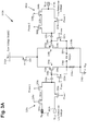
- FIG. 5 shows a diagram of exemplary voltage tolerant interface circuit 510 suitable for use as part of SoC 100 in FIG. 1 , according to yet another implementation.
- exemplary voltage tolerant interface circuit 510 is implemented as a level converter receiving input voltage V IN at input terminal 502 and generating output 504 based on the voltage V IN received at input terminal 502 .
- Voltage tolerant interface circuit 510 having input terminal 502 and providing output 504 corresponds in general to voltage tolerant interface circuit 110 having input terminal 102 and providing output 104 , in FIG. 1 . Consequently, voltage tolerant interface circuits 110 and 510 may share any of the features attributed to either of voltage tolerant interface circuits 110 and 510 in the present disclosure.
- blocking transistor 520 corresponds to blocking transistors 220 a and 220 b , in FIGS. 2A and 2C , as well as to blocking transistor 420 , in FIG. 4A . Thus, blocking transistor 520 may share any of the characteristics attributed to blocking transistors 220 a , 220 b , and 420 in the present disclosure.
- blocking transistor 520 and low-voltage transistor 590 are implemented as N type transistors. Also shown in FIG. 5 are low voltage supply V DD 512 , V SS or ground 516 , and resistor 568 coupled between V DD 512 and low-voltage transistor 590 .
- low-voltage transistor 590 is a transistor having a voltage tolerance of up to approximately 1.0 V.
- low voltage supply V DD 512 may be at 0.9 V and low-voltage transistor 590 may be considered to be coupled to ground at 516 .
- voltage tolerant interface circuit 510 includes blocking transistor 520 and low-voltage transistor 590 in the form of FETs, that representation is merely exemplary. In other implementations, blocking transistor 520 and low-voltage transistor 590 may take the form of any switching devices suitable to the purposes of voltage tolerant interface circuit 510 and/or SoC 100 . Nevertheless, according to the present exemplary implementation, each of blocking transistor 520 and low-voltage transistor 590 takes the form of an NFET. Thus, blocking transistor 520 has source 522 , drain 524 , and gate 526 , while low-voltage transistor 590 is shown to have source 592 , drain 594 , and gate 596 (hereinafter “control terminal 596 ”).
- Blocking transistor 520 has gate 526 biased at a voltage within the voltage tolerance of low-voltage transistor 590 , e.g., up to approximately 0.9 V. As a result of that biasing, blocking transistor 520 is an always-on blocking transistor. Because blocking transistor 520 is always-on, its switching speed is not relevant to the overall performance of voltage tolerant interface circuit 510 . Consequently, blocking transistor 520 may be implemented using one or more small, fast, low-voltage transistors, or using one or more larger, slower, higher voltage tolerant transistors. In one implementation, blocking transistor 520 may take the form of a low-voltage transistor having a voltage tolerance substantially equal to the voltage tolerance of low-voltage transistor 590 , i.e., a voltage tolerance of up to approximately 1.0 V.
- Blocking transistor 520 is coupled between control terminal 596 of low-voltage transistor 590 and input terminal 502 . Because it is biased, blocking transistor 520 will block a portion of V IN when V IN is higher than the biasing voltage applied to gate 526 . In other words, a voltage at source 522 of blocking transistor 520 will not exceed the biasing voltage applied to gate 526 . As a result, blocking transistor 520 protects control terminal 596 of low-voltage transistor 590 by blocking the voltage received at input terminal 502 when V IN exceeds the voltage tolerance of low-voltage transistor 590 .
- blocking transistor 520 clamps the voltage applied to control terminal 596 of low-voltage transistor 590 at approximately that bias voltage.
- blocking transistor 520 passes V IN to control terminal 596 of low-voltage transistor 590 .
- V IN is greater than a turn-on voltage of low-voltage transistor 590 , i.e., the input to voltage tolerant interface circuit 510 is high, output 504 is pulled to ground 512 and is low.
- V IN drops below the turn-on voltage of low-voltage transistor 590 , i.e., the input to voltage tolerant interface circuit 510 is low, output 504 goes high. Consequently, blocking transistor 520 advantageously enables use of low-voltage transistor 590 to implement voltage tolerant interface circuit 510 as an inverter, while also advantageously protecting low-voltage transistor 590 from voltages exceeding its voltage tolerance.
- the present application discloses voltage tolerant interface circuits enabling use of low-voltage transistors in applications in which voltages exceeding the voltage tolerance of those transistors may be present.
- a blocking transistor between a control terminal of a low-voltage transistor and an input terminal to the voltage tolerant interface circuit
- the present inventive principles provide voltage protection for the low-voltage transistor.
- the blocking transistor protects the control terminal of the low-voltage transistor by blocking the voltage received at the input terminal when the voltage exceeds a voltage tolerance of the low-voltage transistor.
- the low-voltage transistor receives a supply voltage higher than its voltage tolerance.
- the blocking transistor protects the control terminal of the low-voltage transistor by blocking the voltage received at the input terminal when the voltage is below a predetermined threshold voltage.
Landscapes
- Physics & Mathematics (AREA)
- Nonlinear Science (AREA)
- Logic Circuits (AREA)
Abstract
Description
Claims (18)
Priority Applications (1)
| Application Number | Priority Date | Filing Date | Title |
|---|---|---|---|
| US17/081,888 US11201616B2 (en) | 2018-10-01 | 2020-10-27 | Voltage tolerant interface circuit |
Applications Claiming Priority (2)
| Application Number | Priority Date | Filing Date | Title |
|---|---|---|---|
| US16/148,232 US10879889B2 (en) | 2018-10-01 | 2018-10-01 | Voltage tolerant circuit and system |
| US17/081,888 US11201616B2 (en) | 2018-10-01 | 2020-10-27 | Voltage tolerant interface circuit |
Related Parent Applications (1)
| Application Number | Title | Priority Date | Filing Date |
|---|---|---|---|
| US16/148,232 Continuation US10879889B2 (en) | 2018-10-01 | 2018-10-01 | Voltage tolerant circuit and system |
Publications (2)
| Publication Number | Publication Date |
|---|---|
| US20210044289A1 US20210044289A1 (en) | 2021-02-11 |
| US11201616B2 true US11201616B2 (en) | 2021-12-14 |
Family
ID=69947995
Family Applications (2)
| Application Number | Title | Priority Date | Filing Date |
|---|---|---|---|
| US16/148,232 Active 2039-06-14 US10879889B2 (en) | 2018-10-01 | 2018-10-01 | Voltage tolerant circuit and system |
| US17/081,888 Active US11201616B2 (en) | 2018-10-01 | 2020-10-27 | Voltage tolerant interface circuit |
Family Applications Before (1)
| Application Number | Title | Priority Date | Filing Date |
|---|---|---|---|
| US16/148,232 Active 2039-06-14 US10879889B2 (en) | 2018-10-01 | 2018-10-01 | Voltage tolerant circuit and system |
Country Status (1)
| Country | Link |
|---|---|
| US (2) | US10879889B2 (en) |
Families Citing this family (2)
| Publication number | Priority date | Publication date | Assignee | Title |
|---|---|---|---|---|
| US10833584B2 (en) | 2015-11-12 | 2020-11-10 | Empower Semiconductor, Inc. | Boot-strapping systems and techniques for circuits |
| US10879889B2 (en) * | 2018-10-01 | 2020-12-29 | Empower Semiconductor, Inc. | Voltage tolerant circuit and system |
Citations (4)
| Publication number | Priority date | Publication date | Assignee | Title |
|---|---|---|---|---|
| US7564317B2 (en) * | 2007-07-06 | 2009-07-21 | Amazing Microelectronic Corporation | High/low voltage tolerant interface circuit and crystal oscillator circuit |
| US9588529B2 (en) * | 2010-09-03 | 2017-03-07 | Skyworks Solutions, Inc. | High-voltage tolerant voltage regulator |
| US10748769B2 (en) | 2018-05-09 | 2020-08-18 | Tokyo Electron Limited | Methods and systems for patterning of low aspect ratio stacks |
| US10879889B2 (en) * | 2018-10-01 | 2020-12-29 | Empower Semiconductor, Inc. | Voltage tolerant circuit and system |
Family Cites Families (5)
| Publication number | Priority date | Publication date | Assignee | Title |
|---|---|---|---|---|
| US6147511A (en) * | 1996-05-28 | 2000-11-14 | Altera Corporation | Overvoltage-tolerant interface for integrated circuits |
| US6144221A (en) * | 1998-07-02 | 2000-11-07 | Seiko Epson Corporation | Voltage tolerant interface circuit |
| US7830200B2 (en) * | 2006-01-17 | 2010-11-09 | Cypress Semiconductor Corporation | High voltage tolerant bias circuit with low voltage transistors |
| US8704591B1 (en) * | 2012-11-08 | 2014-04-22 | Lsi Corporation | High-voltage tolerant biasing arrangement using low-voltage devices |
| US10186945B1 (en) * | 2017-06-30 | 2019-01-22 | Empower Semiconductor | Resonant switching regulator with continuous current |
-
2018
- 2018-10-01 US US16/148,232 patent/US10879889B2/en active Active
-
2020
- 2020-10-27 US US17/081,888 patent/US11201616B2/en active Active
Patent Citations (4)
| Publication number | Priority date | Publication date | Assignee | Title |
|---|---|---|---|---|
| US7564317B2 (en) * | 2007-07-06 | 2009-07-21 | Amazing Microelectronic Corporation | High/low voltage tolerant interface circuit and crystal oscillator circuit |
| US9588529B2 (en) * | 2010-09-03 | 2017-03-07 | Skyworks Solutions, Inc. | High-voltage tolerant voltage regulator |
| US10748769B2 (en) | 2018-05-09 | 2020-08-18 | Tokyo Electron Limited | Methods and systems for patterning of low aspect ratio stacks |
| US10879889B2 (en) * | 2018-10-01 | 2020-12-29 | Empower Semiconductor, Inc. | Voltage tolerant circuit and system |
Also Published As
| Publication number | Publication date |
|---|---|
| US20200106431A1 (en) | 2020-04-02 |
| US10879889B2 (en) | 2020-12-29 |
| US20210044289A1 (en) | 2021-02-11 |
Similar Documents
| Publication | Publication Date | Title |
|---|---|---|
| KR102283135B1 (en) | Electrostatic discharge protection circuitry | |
| US10581423B1 (en) | Fault tolerant low leakage switch | |
| TWI645279B (en) | Voltage reference buffer circuit | |
| US9419571B2 (en) | Precision, high voltage, low power differential input stage with static and dynamic gate protection | |
| US11201616B2 (en) | Voltage tolerant interface circuit | |
| CN112513771B (en) | Dual Input LDO Voltage Regulator | |
| US11509224B2 (en) | Dual mode supply circuit and method | |
| EP3548982B1 (en) | Voltage clamp circuit | |
| US10186958B2 (en) | Input-output circuits | |
| US20060232304A1 (en) | Apparatus and methods for adaptive trip point detection | |
| US20230083606A1 (en) | Dual mode supply circuit and method | |
| US11489519B2 (en) | Analog switch with boost current for fast turn on | |
| CN111756029A (en) | High-speed wide dynamic range input structure | |
| KR19990083514A (en) | CMOS reference voltage generator | |
| US10211823B2 (en) | Method and apparatus for protecting gate-source junction of low-voltage MOSFET in high-voltage circuit | |
| US9570906B2 (en) | Voltage clamping circuit | |
| US11502674B2 (en) | Optimized low Ron flatness gate driver | |
| US20040189356A1 (en) | Power-on detector, and power-on reset circuit using the same | |
| US12316330B2 (en) | Comparator circuit with dynamic hysteresis | |
| US9030790B1 (en) | Low-leakage ESD protection circuit | |
| US10429877B1 (en) | Low-voltage reference current circuit | |
| JP2000252429A (en) | Static electricity protection circuit and semiconductor integrated circuit | |
| US20250370491A1 (en) | Device and Method for Generating a Temperature-Independent Reference Voltage | |
| US20240340001A1 (en) | Clamp circuits | |
| US11101780B2 (en) | Comparator circuit |
Legal Events
| Date | Code | Title | Description |
|---|---|---|---|
| FEPP | Fee payment procedure |
Free format text: ENTITY STATUS SET TO UNDISCOUNTED (ORIGINAL EVENT CODE: BIG.); ENTITY STATUS OF PATENT OWNER: SMALL ENTITY |
|
| FEPP | Fee payment procedure |
Free format text: ENTITY STATUS SET TO SMALL (ORIGINAL EVENT CODE: SMAL); ENTITY STATUS OF PATENT OWNER: SMALL ENTITY |
|
| STPP | Information on status: patent application and granting procedure in general |
Free format text: APPLICATION DISPATCHED FROM PREEXAM, NOT YET DOCKETED |
|
| STPP | Information on status: patent application and granting procedure in general |
Free format text: DOCKETED NEW CASE - READY FOR EXAMINATION |
|
| STPP | Information on status: patent application and granting procedure in general |
Free format text: NON FINAL ACTION MAILED |
|
| STPP | Information on status: patent application and granting procedure in general |
Free format text: NON FINAL ACTION MAILED |
|
| STPP | Information on status: patent application and granting procedure in general |
Free format text: RESPONSE TO NON-FINAL OFFICE ACTION ENTERED AND FORWARDED TO EXAMINER |
|
| AS | Assignment |
Owner name: EMPOWER SEMICONDUCTOR, CALIFORNIA Free format text: ASSIGNMENT OF ASSIGNORS INTEREST;ASSIGNOR:OAK, PARAG;REEL/FRAME:057402/0966 Effective date: 20180926 |
|
| STPP | Information on status: patent application and granting procedure in general |
Free format text: NOTICE OF ALLOWANCE MAILED -- APPLICATION RECEIVED IN OFFICE OF PUBLICATIONS |
|
| STPP | Information on status: patent application and granting procedure in general |
Free format text: PUBLICATIONS -- ISSUE FEE PAYMENT VERIFIED |
|
| STCF | Information on status: patent grant |
Free format text: PATENTED CASE |
|
| MAFP | Maintenance fee payment |
Free format text: PAYMENT OF MAINTENANCE FEE, 4TH YR, SMALL ENTITY (ORIGINAL EVENT CODE: M2551); ENTITY STATUS OF PATENT OWNER: SMALL ENTITY Year of fee payment: 4 |