US11194239B2 - Wavelength conversion module and projection device - Google Patents
Wavelength conversion module and projection device Download PDFInfo
- Publication number
- US11194239B2 US11194239B2 US16/879,752 US202016879752A US11194239B2 US 11194239 B2 US11194239 B2 US 11194239B2 US 202016879752 A US202016879752 A US 202016879752A US 11194239 B2 US11194239 B2 US 11194239B2
- Authority
- US
- United States
- Prior art keywords
- wavelength conversion
- region
- reflective layer
- substrate
- layer
- Prior art date
- Legal status (The legal status is an assumption and is not a legal conclusion. Google has not performed a legal analysis and makes no representation as to the accuracy of the status listed.)
- Active
Links
- 238000006243 chemical reaction Methods 0.000 title claims abstract description 232
- 239000000758 substrate Substances 0.000 claims abstract description 112
- 238000005286 illumination Methods 0.000 claims abstract description 39
- 239000000463 material Substances 0.000 claims description 57
- 230000005284 excitation Effects 0.000 claims description 55
- 230000005540 biological transmission Effects 0.000 claims description 15
- 238000009792 diffusion process Methods 0.000 claims description 6
- 238000001228 spectrum Methods 0.000 claims description 6
- 239000010410 layer Substances 0.000 description 109
- 230000008901 benefit Effects 0.000 description 13
- 230000000694 effects Effects 0.000 description 12
- OAICVXFJPJFONN-UHFFFAOYSA-N Phosphorus Chemical compound [P] OAICVXFJPJFONN-UHFFFAOYSA-N 0.000 description 7
- 230000001010 compromised effect Effects 0.000 description 6
- 229920001296 polysiloxane Polymers 0.000 description 6
- VYPSYNLAJGMNEJ-UHFFFAOYSA-N Silicium dioxide Chemical compound O=[Si]=O VYPSYNLAJGMNEJ-UHFFFAOYSA-N 0.000 description 4
- 230000006866 deterioration Effects 0.000 description 4
- 230000002349 favourable effect Effects 0.000 description 4
- 230000003287 optical effect Effects 0.000 description 4
- 238000002310 reflectometry Methods 0.000 description 4
- 239000003086 colorant Substances 0.000 description 3
- 239000002245 particle Substances 0.000 description 3
- 230000000149 penetrating effect Effects 0.000 description 3
- BQCADISMDOOEFD-UHFFFAOYSA-N Silver Chemical compound [Ag] BQCADISMDOOEFD-UHFFFAOYSA-N 0.000 description 2
- MCMNRKCIXSYSNV-UHFFFAOYSA-N ZrO2 Inorganic materials O=[Zr]=O MCMNRKCIXSYSNV-UHFFFAOYSA-N 0.000 description 2
- 229910052782 aluminium Inorganic materials 0.000 description 2
- XAGFODPZIPBFFR-UHFFFAOYSA-N aluminium Chemical compound [Al] XAGFODPZIPBFFR-UHFFFAOYSA-N 0.000 description 2
- 239000011248 coating agent Substances 0.000 description 2
- 238000000576 coating method Methods 0.000 description 2
- 238000005516 engineering process Methods 0.000 description 2
- 230000006870 function Effects 0.000 description 2
- 230000000670 limiting effect Effects 0.000 description 2
- 238000012986 modification Methods 0.000 description 2
- 230000004048 modification Effects 0.000 description 2
- TWNQGVIAIRXVLR-UHFFFAOYSA-N oxo(oxoalumanyloxy)alumane Chemical compound O=[Al]O[Al]=O TWNQGVIAIRXVLR-UHFFFAOYSA-N 0.000 description 2
- RVTZCBVAJQQJTK-UHFFFAOYSA-N oxygen(2-);zirconium(4+) Chemical compound [O-2].[O-2].[Zr+4] RVTZCBVAJQQJTK-UHFFFAOYSA-N 0.000 description 2
- 230000036961 partial effect Effects 0.000 description 2
- 239000000377 silicon dioxide Substances 0.000 description 2
- 229910052709 silver Inorganic materials 0.000 description 2
- 239000004332 silver Substances 0.000 description 2
- PZNSFCLAULLKQX-UHFFFAOYSA-N Boron nitride Chemical compound N#B PZNSFCLAULLKQX-UHFFFAOYSA-N 0.000 description 1
- GWEVSGVZZGPLCZ-UHFFFAOYSA-N Titan oxide Chemical compound O=[Ti]=O GWEVSGVZZGPLCZ-UHFFFAOYSA-N 0.000 description 1
- 230000008878 coupling Effects 0.000 description 1
- 238000010168 coupling process Methods 0.000 description 1
- 238000005859 coupling reaction Methods 0.000 description 1
- 230000010354 integration Effects 0.000 description 1
- 239000004973 liquid crystal related substance Substances 0.000 description 1
- 229910052751 metal Inorganic materials 0.000 description 1
- 239000002184 metal Substances 0.000 description 1
- 239000000203 mixture Substances 0.000 description 1
- 230000035515 penetration Effects 0.000 description 1
- 238000007639 printing Methods 0.000 description 1
- 230000000750 progressive effect Effects 0.000 description 1
- 239000011241 protective layer Substances 0.000 description 1
- 230000002829 reductive effect Effects 0.000 description 1
- 229910052710 silicon Inorganic materials 0.000 description 1
- 239000010703 silicon Substances 0.000 description 1
- 235000012239 silicon dioxide Nutrition 0.000 description 1
- 239000007787 solid Substances 0.000 description 1
- 238000005507 spraying Methods 0.000 description 1
Images


Classifications
-
- G—PHYSICS
- G03—PHOTOGRAPHY; CINEMATOGRAPHY; ANALOGOUS TECHNIQUES USING WAVES OTHER THAN OPTICAL WAVES; ELECTROGRAPHY; HOLOGRAPHY
- G03B—APPARATUS OR ARRANGEMENTS FOR TAKING PHOTOGRAPHS OR FOR PROJECTING OR VIEWING THEM; APPARATUS OR ARRANGEMENTS EMPLOYING ANALOGOUS TECHNIQUES USING WAVES OTHER THAN OPTICAL WAVES; ACCESSORIES THEREFOR
- G03B21/00—Projectors or projection-type viewers; Accessories therefor
- G03B21/14—Details
- G03B21/20—Lamp housings
- G03B21/2006—Lamp housings characterised by the light source
- G03B21/2033—LED or laser light sources
- G03B21/204—LED or laser light sources using secondary light emission, e.g. luminescence or fluorescence
-
- G—PHYSICS
- G03—PHOTOGRAPHY; CINEMATOGRAPHY; ANALOGOUS TECHNIQUES USING WAVES OTHER THAN OPTICAL WAVES; ELECTROGRAPHY; HOLOGRAPHY
- G03B—APPARATUS OR ARRANGEMENTS FOR TAKING PHOTOGRAPHS OR FOR PROJECTING OR VIEWING THEM; APPARATUS OR ARRANGEMENTS EMPLOYING ANALOGOUS TECHNIQUES USING WAVES OTHER THAN OPTICAL WAVES; ACCESSORIES THEREFOR
- G03B21/00—Projectors or projection-type viewers; Accessories therefor
- G03B21/14—Details
- G03B21/20—Lamp housings
- G03B21/2066—Reflectors in illumination beam
-
- G—PHYSICS
- G03—PHOTOGRAPHY; CINEMATOGRAPHY; ANALOGOUS TECHNIQUES USING WAVES OTHER THAN OPTICAL WAVES; ELECTROGRAPHY; HOLOGRAPHY
- G03B—APPARATUS OR ARRANGEMENTS FOR TAKING PHOTOGRAPHS OR FOR PROJECTING OR VIEWING THEM; APPARATUS OR ARRANGEMENTS EMPLOYING ANALOGOUS TECHNIQUES USING WAVES OTHER THAN OPTICAL WAVES; ACCESSORIES THEREFOR
- G03B21/00—Projectors or projection-type viewers; Accessories therefor
- G03B21/14—Details
- G03B21/20—Lamp housings
- G03B21/208—Homogenising, shaping of the illumination light
Definitions
- the invention relates to an optical module and an optical device, and in particular, to a wavelength conversion module and a projection device.
- Solid-state light sources such as light-emitting diodes (LEDs) and laser diodes have been recently drawing more and more attention in the market. Since the laser diodes have a luminous efficiency higher than about 20%, a technology of combing phosphor with a laser light source to form a solid color light source used for a projector has been under progressive development.
- a phosphor wheel in general, includes a substrate, a wavelength conversion layer and a reflective layer.
- the wavelength conversion layer may be formed by applying phosphor mixed with silicone onto the substrate.
- a wavelength conversion layer made of phosphor mixed with silicone may, for example, not be effectively resistant to a high temperature and may be easily deteriorated. After a long time of working, the silicone may be deteriorated or be burned out. Thus, the luminous efficiency and reliability of the phosphor wheel may be affected.
- the reflective layer of a phosphor wheel may be produced in two modes.
- a reflective layer is formed by coating a silver film, an aluminum film, a dielectric film, or a mixed stacking thereof on a substrate in vacuum.
- Such a reflective layer may have the advantages of high temperature resistance and fast heat conduction.
- the reflective layer may preset different reflectances for color light beams of different wavebands, it is difficult to achieve a favorable reflection effect across various color lights at the same time.
- a reflective layer is formed by mixing diffuse reflection particles with silicone and then coating the mixture on the substrate by ways of printing, spraying and dispensing, etc.
- the silicone contained in such a reflective layer may have a risk of being not resistant to a high temperature and being easily deteriorated or burned out.
- the invention provides a wavelength conversion module, which has good conversion efficiency and reliability.
- the invention provides a projection device, which has good conversion efficiency and reliability.
- an embodiment of the invention provides a wavelength conversion module.
- the wavelength conversion module includes a substrate, a wavelength conversion layer, a first reflective layer, and a second reflective layer.
- the substrate includes a first region and a second region.
- the wavelength conversion layer is disposed on the substrate.
- the first reflective layer is disposed on the first region of the substrate, and the first reflective layer is located between the first region of the substrate and the wavelength conversion layer.
- the second reflective layer is disposed on the second region of the substrate, and the second reflective layer is located between the second region of the substrate and the wavelength conversion layer.
- a distance from a top surface of the second reflective layer to the substrate is shorter than a distance from a top surface of the first reflective layer to the substrate.
- an embodiment of the invention provides a projection device.
- the projection device includes an illumination system, a light valve and a projection lens.
- the illumination system is configured to provide an illumination beam, and includes an excitation light source, the wavelength conversion module and a filter module.
- the excitation light source may emit an excitation beam
- the wavelength conversion module is located on a transmission path of the excitation beam, and configured to convert the excitation beam into at least one converted beam.
- the filter module is located on a transmission path of the excitation beam and the at least one converted beam.
- the illumination beam includes the excitation beam and the at least one converted beam.
- the light valve is located on a transmission path of the illumination beam and may convert the illumination beam into an image beam.
- the projection lens is located on a transmission path of the image beam and may project the image beam.
- the embodiments of the invention may have at least one of the following advantages or effects.
- the first reflective layer and the second reflective layer are disposed at different regions distinctively or compositely, so that different reflection structures may be used for various excitation beams of different energy intensities. With such a reflection configuration, deterioration or burnout caused from a high temperature may be effectively avoided, and the conversion efficiency and reliability of the wavelength conversion module and the projection device may also not be compromised.
- FIG. 1 is a schematic structural view of a projection device according to an embodiment of the invention.
- FIG. 2A is a schematically exploded view of a wavelength conversion module of FIG. 1 .
- FIG. 2B is a schematic view of a perspective of the wavelength conversion module of FIG. 2A .
- FIG. 2C is a schematically sectional view of the wavelength conversion module of FIG. 2B along a line A-A.
- FIG. 2D is a schematically enlarged view of a partial region of the wavelength conversion module of FIG. 2B .
- FIG. 2E schematically shows the reflectivity of the first reflective layer of FIG. 2D for light beams ranging within a wavelength band.
- FIG. 2F schematically shows the reflectivity of the second reflective layer of FIG. 2D for light beams ranging within a wavelength band.
- FIG. 2G is a schematic front view of the wavelength conversion module of FIG. 2A .
- FIG. 2H is a schematic front view of a filter module of FIG. 1 .
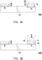
- FIG. 3A is a schematically sectional view of another wavelength conversion module of FIG. 1 .
- FIG. 3B is a schematically sectional view of another wavelength conversion module of FIG. 1 .
- FIG. 4 is a schematically structural view of another projection device according to an embodiment of the invention.
- the description of “A” component facing “B” component herein may contain the situations that “A” component directly faces “B” component or one or more additional components are between “A” component and “B” component.
- the description of “A” component “adjacent to” “B” component herein may contain the situations that “A” component is directly “adjacent to” “B” component or one or more additional components are between “A” component and “B” component. Accordingly, the drawings and descriptions will be regarded as illustrative in nature and not as restrictive.
- FIG. 1 is a schematic structural view of a projection device according to an embodiment of the invention.
- the projection device 300 includes an illumination system 200 , a light valve 310 and a projection lens 320 .
- the illumination system 200 is configured to provide an illumination beam 70 .
- the light valve 310 is located on a transmission path of the illumination beam 70 and may be configured to convert the illumination beam 70 into an image beam 80 .
- the projection lens 320 is located on a transmission path of the image beam 80 and may be configured to project the image beam 80 onto a screen (not shown) to form an image picture.
- the light valve 310 includes, for example, a digital micro-mirror device (DMD) or a liquid-crystal-on-silicon (LCOS) panel.
- the light valve 310 may also be a penetrative liquid crystal panel or another beam modulator.
- the projection lens 320 may include one or more lenses.
- the beam splitter 220 is disposed on a transmission path of the excitation beam 50 and located between the excitation light source 210 and the wavelength conversion module 100 .
- the beam splitter 220 may be a partially-penetrative and partially-reflective element, a dichroic mirror, a polarizing beam splitting element, or other various elements that may be configured to split beams.
- the beam splitter 220 may, for example, allow a blue band beam to penetrate while reflecting beams of other color (e.g., red, green, yellow, etc.). That is to say, the beam splitter 220 may allow a blue excitation beam 50 to penetrate, and thus, the excitation beam 50 may penetrate the beam splitter 220 and may be transmitted and emitted into the wavelength conversion module 100 .
- the wavelength conversion module 100 of this embodiment will be further explained below with reference to FIG. 2A to FIG. 2H .
- FIG. 2A is a schematically exploded view of a wavelength conversion module of FIG. 1 .
- FIG. 2B is a schematic view of a perspective of the wavelength conversion module of FIG. 2A .
- FIG. 2C is a schematically sectional view of the wavelength conversion module of FIG. 2B along a line A-A.
- FIG. 2D is a schematically enlarged view of a partial region R of the wavelength conversion module of FIG. 2B .
- the wavelength conversion module 100 is located on the transmission path of the excitation beam 50 .
- a wavelength conversion layer 130 includes a first wavelength conversion region WR 1 , a second wavelength conversion region WR 2 and a passing-through region TR.
- the first wavelength conversion region WR 1 and the second wavelength conversion region WR 2 of the wavelength conversion module 100 may respectively convert the excitation beam 50 into a converted beam 60 Y and a converted beam 60 G, and the passing-through region TR of the wavelength conversion module 100 allows the excitation beam 50 to pass through.
- the excitation beam 50 passing through the passing-through region TR may then be transmitted to a subsequent optical element.
- both the first wavelength conversion material and the second wavelength conversion material are located in the first wavelength conversion region WR 1 , and correspond to the first region R 1 and the second region R 2 of the substrate 110 , respectively.
- the wavelength conversion layer 130 further includes a third wavelength conversion material located in the second wavelength conversion region WR 2 .
- the substrate 100 further includes a third region R 3 , and the third wavelength conversion material is correspondingly disposed on the third region R 3 of the substrate 110 .
- the first wavelength conversion material and the second wavelength conversion material are phosphors that may be excited to generate yellow light.
- the third wavelength conversion material may include a phosphor that may be excited to generate green light.
- the converted beam 60 Y may be yellow light
- the converted beam 60 G may be green light.
- the first wavelength conversion material and the second wavelength conversion material may be different or not.
- the converted beams 60 Y converted by the first wavelength conversion material and the second wavelength conversion material are yellow light, while the dominant wavelength of the color light formed from the first wavelength conversion material is different from the dominant wavelength of the color light formed from the second wavelength conversion material.
- the color of the subsequently formed illumination beam 70 can be further adjusted as required by various combination of the first wavelength conversion material and the second wavelength conversion material.
- the first reflective layer 121 is disposed on the first region R 1 of the substrate 110 , and the first reflective layer 121 is located between the first region R 1 of the substrate 110 and the wavelength conversion layer 130 .
- the second reflective layer 122 is disposed on the second region R 2 of the substrate 110 , and the second reflective layer 122 is located between the second region R 2 of the substrate 110 and the wavelength conversion layer 130 .
- a distance D 2 from a top surface of the second reflective layer 122 in the second region R 2 to the substrate 110 is shorter than a distance D 1 from a top surface of the first reflective layer 121 in the first region R 1 to the substrate 110 .
- a thickness T 2 of the second reflective layer 122 in the second region R 2 is less than a thickness T 1 of the first reflective layer 121 in the first region R 1 .
- the second reflective layer 122 may be also selectively disposed on the first region R 111 of the substrate 110 .
- the second reflective layer 122 may be also located between the first region R 1 of the substrate 110 and the first reflective layer 121 .
- the invention does not limit the range of the second reflective layer 122 as long as the distance D 2 from the top surface of the second reflective layer 122 on the second region R 2 of the substrate 110 to the substrate 110 is shorter than the distance D 1 from the top surface of the first reflective layer 121 (in the first region R 1 ) to the substrate 110 .
- the wavelength conversion layer 130 on the second region R 2 of the substrate 110 is closer to the substrate 110 , and the heat generated from the wavelength conversion layer 130 may be quickly conducted to the substrate 110 , thereby achieving a higher temperature resistance and a faster heat conduction.
- the wavelength conversion layer 130 located in the first region R 1 and the wavelength conversion layer located in the second region R 2 may be located on different planes.
- the invention is not limited thereto.
- the wavelength conversion layer 130 located in the first region R 1 and the wavelength conversion layer located in the second region R 2 may be located on the same plane.
- the first reflective layer 121 and/or the second reflective layer 122 may be disposed between the third region R 3 of the substrate 110 and the second wavelength conversion region WR 2 of the wavelength conversion layer 130 .
- the first reflective layer 121 is a diffuse reflection layer
- the second reflective layer 122 is a specular reflection layer
- the diffuse reflection layer may be a reflective layer mixed with white scattering particles and a bonding material.
- the material of the scattering particles may include titanium dioxide (TiO 2 ), silicon dioxide (SiO 2 ), aluminum oxide (Al 2 O 3 ), boron nitride (BN), or zirconium dioxide (ZrO 2 ).
- the material of the bonding material may include silicone, but the invention is not limited thereto.
- the specular reflection layer may be a metal layer with a protective layer or a dielectric layer coated on the surface of the substrate 110 , and the material thereof may include silver or aluminum, but the invention is not limited thereto.
- FIG. 2E schematically shows the reflectivity of the first reflective layer of FIG. 2D for light beams ranging within a wavelength band.
- FIG. 2F schematically shows the reflectivity of the second reflective layer of FIG. 2D for light beams ranging within a wavelength band.
- a first reflection spectrum of the first reflective layer 121 for a light beam ranging within a specific wavelength band is different from a second reflection spectrum of the second reflective layer 122 for the light beam ranging within the specific wavelength band.
- the first reflective layer 121 may have an optimal reflection effect for various color lights.
- the second reflective layer 122 may have a favorable reflection effect on a long-wavelength light beam.
- the wavelength conversion layer 130 located on the second region R 2 of the substrate 110 may exhibit a higher heat resistance and a faster heat conduction, and the conversion efficiency for long-wavelength light beams and the reliability not be compromised.
- the wavelength conversion layer 130 located on the first region R 1 of the substrate 110 may maintain the conversion efficiency for various color light beams of different wavelengths.
- FIG. 2G is a schematic front view of the wavelength conversion module 100 of FIG. 2A .
- FIG. 2H is a schematic front view of the filter module 230 of FIG. 1 .
- the substrate 110 of the wavelength conversion module 100 may include a hollowed region (not numbered), which is positioned corresponding to the passing-through region TR, and the wavelength conversion module 100 further may include a diffusion piece 140 , which is positioned corresponding to the passing-through region TR and the hollowed region (not numbered) of the substrate 110 .
- the wavelength conversion module 100 may be a penetrative wavelength conversion module 100 , and the passing-through region TR may allow penetration of the excitation beam 50 .
- the wavelength conversion module 100 further includes a first driving device MR 1 , and the first driving device MR 1 may be used for driving the passing-through region TR and the at least one wavelength conversion region WR to rotate so that they may enter an illumination range of the excitation beam 50 at different times. Therefore, the excitation beam 50 may selectively pass through the passing-through region TR or be converted into the converted beams 60 Y, 60 G. As shown in FIG. 1 , in the embodiment, when the passing-through region TR of the wavelength conversion module 100 enters the illumination range of the excitation beam 50 , the excitation beam 50 penetrates the wavelength conversion module 100 and is transmitted to the filter module 230 via a light transmission module LT.
- the excitation beam 50 may be converted into the converted beams 60 Y, 60 G by the wavelength conversion region WR 1 or the wavelength conversion region WR 2 . Thereafter, as shown in FIG. 1 , at least one of the converted beams 60 Y, 60 G from the wavelength conversion module 100 may be guided to the beam splitter 220 and reflected to the subsequent filter module 230 .
- the filter module 230 may be located on the transmission path of the excitation beam 50 and the converted beams 60 Y, 60 G, and the filter module 230 may have a first filter region FR 1 , a second filter region FR 2 , a third filter region FR 3 , and a diffusion region DR.
- the filter module 230 further includes a second driving device (not shown), which may be used to drive the first filter region FR 1 and the second filter region FR 2 to rotate, such that they may enter the illumination range of the converted beams 60 Y, 60 G correspondingly at different times to respectively form color lights of different colors.
- the converted beam from the first wavelength conversion material in the first wavelength conversion region WR 1 may pass through the first filter region FR 1 and a first color light beam Y may be formed
- the converted beam from the second wavelength conversion material in the first wavelength conversion region WR 1 may pass through the second filter region FR 2 and a second color light beam R may be formed
- the converted beam from the third wavelength conversion material in the second wavelength conversion region WR 2 may pass through the third filter region FR 3 and a fourth color light beam G may be formed.
- the diffusion region DR may periodically enter the illumination range of the excitation beam 50 , and the diffused excitation beam 50 may then be transmitted to the filter module 230 at different times and a third color light beam B may be formed.
- the first color light Y may be yellow light
- the second color light R may be red light
- the fourth color light G may be green light
- the third color light B may be blue light
- the illumination beam 70 may include the first color light Y, the second color light R, the third color light B, and the fourth color light G.
- the excitation beam 50 and the converted beams 60 Y, 60 G may be converted sequentially into the illumination beam 70 of a plurality of different colors.
- the filter module 230 may filter out a part of the converted beam 60 Y and the second color light R may thus be formed, the conversion efficiency of the second color light R may be relatively reduced with respect to the first color light Y.
- the wavelength conversion layer 130 located on the second region R 2 may excited by an excitation beam 50 with a higher intensity to generate a converted beam 60 Y with a sufficient brightness, such that the intensity and proportion of the second color light R in the illumination beam 70 may be maintained.
- the driving current for the excitation light source 210 may be adjusted with time to generate excitation beams 50 of different intensities, so that intensities of various color lights beams may be adjusted and combined to form different and desirable colorful beams for a desired colorful picture.
- the wavelength conversion module 100 may easily conduct heat, and thus exhibits a higher heat resistance and a faster heat conduction, while the conversion efficiency for long-wavelength light beams and the reliability not be compromised. Therefore, the risk of poor conversion efficiency or burnout may be avoided effectively.
- the second wavelength conversion material on the second region R 2 may closer to the substrate 110 , that is, closer to the substrate, so that the problem of poor conversion efficiency or burnout caused from a high temperature may be alleviated.
- the first color light Y formed from the filter module 230 may be ranged in a wider waveband, and with the arrangement of the first reflective layer 121 , the wavelength conversion layer 130 corresponding to the first region R 1 of the substrate 110 may be configured to maintain a favorable conversion efficiency for color lights of different wavebands.
- the projection device 300 further includes a light homogenizing element 240 located on the transmission path of the illumination beam 70 .
- the light homogenizing element 240 includes an integration column, but the invention is not limited thereto.
- the light homogenizing element 240 may be used to homogenize the illumination beam 70 and transmit the illumination beam 70 to the light valve 310 .
- the first reflective layer 121 and the second reflective layer 122 are disposed at different regions distinctively or compositely, so that different reflection structures may be used for various excitation beams of different energy intensities.
- deterioration or burnout caused from a high temperature may be effectively avoided, and the conversion efficiency and reliability of the wavelength conversion module 100 may also not be compromised.
- first reflective layer 121 and the second reflective layer 122 of the wavelength conversion module 100 are respectively exemplified by a diffuse reflection layer and a specular reflection layer, the invention is not limited thereto. In other embodiments, the first reflective layer 121 and the second reflective layer 122 may both be specular reflection layers.
- the first reflective layer 121 may include a plurality of first sub-reflective layers
- the second reflective layer 122 may also include a plurality of second sub-reflective layers
- the number of the plurality of first sub-reflective layers is different from the number of the plurality of second sub-reflective layers.
- the distance D 2 from the top surface of the second reflective layer 122 on the second region R 2 of the substrate 110 to the substrate 110 is shorter than the distance D 1 from the top surface of the first reflective layer 121 on the first region R 1 of the substrate 110 to the substrate 110 .
- the first reflective layer 121 may have an optimal reflection effect for various color lights (e.g., visible light having a wavelength band of 400 nm to 700 nm), and the second reflective layer 122 may have a favorable reflection effect on a long-wavelength light beam.
- FIG. 3A is a schematically sectional view of another example of the wavelength conversion module 100 of FIG. 1 .
- FIG. 3B is a schematically sectional view of still another example of the wavelength conversion module 100 of FIG. 1 .
- a wavelength conversion module 100 A and a wavelength conversion module 100 B are similar to the wavelength conversion module 100 of FIG. 2C , and the differences therebetween may be described as follows.
- the first region R 1 of the substrate 110 of the wavelength conversion module 100 A may include a groove CA configured to accommodate the first reflective layer 121 .
- FIG. 3A the first region R 1 of the substrate 110 of the wavelength conversion module 100 A may include a groove CA configured to accommodate the first reflective layer 121 .
- a width W 1 of the wavelength conversion layer 130 of the wavelength conversion module 100 B across the first region R 1 is greater than a width W 2 of the first reflective layer 121 .
- the wavelength conversion layer 130 may completely cover the first reflective layer 121 .
- the invention does not limit the structure used for accommodating the first reflective layer 121 or the width of the first reflective layer 121 .
- the first reflective layer 121 and the second reflective layer 122 are disposed at different regions distinctively or compositely, so that different reflection structures may be used for various excitation beams of different energy intensities.
- deterioration or burnout caused from a high temperature may be effectively avoided, and the conversion efficiency and reliability of the wavelength conversion module 100 A and the wavelength conversion module 100 B may also not be compromised.
- the wavelength conversion module 100 A and the wavelength conversion module 100 B may also achieve similar functions to the wavelength conversion module 100 of FIG. 2C , and may have similar effects and advantages to the wavelength conversion module 100 .
- the descriptions may not be repeated hereinafter.
- the wavelength conversion module 100 A and the wavelength conversion module 100 B are applied to the illumination system 200 of the projection device 300 of FIG. 1 , the effects and advantages of the aforementioned projection device 300 may also be achieved, and the relative descriptions may not be repeated hereinafter.
- the projection device 300 is exemplified by the penetrative wavelength conversion module 100 , but the invention is not limited thereto.
- the projection device 300 may also include a reflective wavelength conversion module, and people of ordinary skill in the art may make appropriate changes to an optical path referring to the invention, and similar effects and advantages to the aforementioned projection device 300 may be achieved, but it should still fall within the scope of the invention. Some examples are given below as an illustration.
- FIG. 4 is a schematically structural view of another projection device 300 A according to an embodiment of the invention.
- the projection device 300 A may include a wavelength conversion module 100 C.
- the wavelength conversion module 100 C may be similar to the wavelength conversion module 100 with the following difference.
- the wavelength conversion module 100 C is a reflective wavelength conversion module. Therefore, the substrate 110 of the wavelength conversion module 100 C may not include a hollowed region.
- a reflection region may be disposed on the wavelength conversion module 100 C to reflect the excitation beam 50 .
- the excitation beam 50 when the reflection region of the wavelength conversion module 100 C enters the illumination range of the excitation beam 50 , the excitation beam 50 may be reflected by the reflection region, and then guided to the beam splitter 220 . The excitation beam 50 may further be reflected to the subsequent filter module 230 .
- the excitation beam 50 when the first wavelength conversion region WR 1 or the second wavelength conversion region WR 2 enters the irradiation range of the excitation beam 50 , the excitation beam 50 may be converted into the converted beam 60 Y or 60 G by the first wavelength conversion region WR 1 or the second wavelength conversion region WR 2 . Thereafter, as shown in FIG.
- the converted beams 60 Y, 60 G from the wavelength conversion module 100 C may be guided to the beam splitter 220 and be reflected to the subsequent filter module 230 . Then, the first filter region FR 1 , the second filter region FR 2 and the third filter region FR 3 of the filter module 230 enter the illumination range of the converted beams 60 Y, 60 G correspondingly at different times to respectively form the first color light Y, the second color light R and the fourth color light G.
- the diffusion region of the filter module 230 may periodically enter the illumination range of the excitation beam 50 , and the diffused excitation beam 50 may then be transmitted to the filter module 230 at different times and the third color light B may be formed, thereby forming the subsequent illumination beam 70 and image beam 80 .
- the wavelength conversion module 100 C employed in the projection device 300 A may be similar to the wavelength conversion module 100 , similar functions, effects, or advantages may be achieved, so the projection device 300 A may also achieve effects and advantages similar to the projection device 300 .
- the relative descriptions may not be repeated hereinafter.
- the embodiments of the invention have at least one of the following advantages or effects.
- the first reflective layer and the second reflective layer are disposed at different regions distinctively or compositely, so that different reflection structures may be used for various excitation beams of different energy intensities. With such a reflection configuration, deterioration or burnout caused from a high temperature may be effectively avoided, and the conversion efficiency and reliability of the wavelength conversion module and the projection device may also not be compromised.
- the term “the invention”, “the present invention” or the like does not necessarily limit the claim scope to a specific embodiment, and the reference to particularly preferred exemplary embodiments of the invention does not imply a limitation on the invention, and no such limitation is to be inferred.
- the invention is limited only by the spirit and scope of the appended claims. Moreover, these claims may refer to use “first”, “second”, etc. following with noun or element. Such terms should be understood as a nomenclature and should not be construed as giving the limitation on the number of the elements modified by such nomenclature unless specific number has been given.
- the abstract of the disclosure is provided to comply with the rules requiring an abstract, which will allow a searcher to quickly ascertain the subject matter of the technical disclosure of any patent issued from this disclosure.
Landscapes
- Physics & Mathematics (AREA)
- General Physics & Mathematics (AREA)
- Engineering & Computer Science (AREA)
- Multimedia (AREA)
- Optics & Photonics (AREA)
- Projection Apparatus (AREA)
- Non-Portable Lighting Devices Or Systems Thereof (AREA)
Abstract
Description
Claims (25)
Applications Claiming Priority (2)
| Application Number | Priority Date | Filing Date | Title |
|---|---|---|---|
| CN201920757029.2 | 2019-05-24 | ||
| CN201920757029.2U CN210072201U (en) | 2019-05-24 | 2019-05-24 | Wavelength conversion module and projection device |
Publications (2)
| Publication Number | Publication Date |
|---|---|
| US20200371414A1 US20200371414A1 (en) | 2020-11-26 |
| US11194239B2 true US11194239B2 (en) | 2021-12-07 |
Family
ID=69454016
Family Applications (1)
| Application Number | Title | Priority Date | Filing Date |
|---|---|---|---|
| US16/879,752 Active US11194239B2 (en) | 2019-05-24 | 2020-05-20 | Wavelength conversion module and projection device |
Country Status (2)
| Country | Link |
|---|---|
| US (1) | US11194239B2 (en) |
| CN (1) | CN210072201U (en) |
Families Citing this family (5)
| Publication number | Priority date | Publication date | Assignee | Title |
|---|---|---|---|---|
| CN113625515B (en) * | 2020-05-08 | 2023-07-04 | 中强光电股份有限公司 | Wavelength conversion device and projection device |
| CN114967303B (en) | 2021-02-26 | 2024-08-27 | 中强光电股份有限公司 | Wavelength conversion device, manufacturing method thereof and projector |
| CN216361908U (en) * | 2021-10-21 | 2022-04-22 | 中强光电股份有限公司 | Wavelength conversion element and projection device |
| CN115095804A (en) * | 2022-05-30 | 2022-09-23 | 扬州吉新光电有限公司 | Light source system |
| US20240402585A1 (en) * | 2023-06-05 | 2024-12-05 | Coretronic Corporation | Wavelength conversion module and projection device |
Citations (5)
| Publication number | Priority date | Publication date | Assignee | Title |
|---|---|---|---|---|
| US20170180686A1 (en) | 2015-12-18 | 2017-06-22 | Coretronic Corporation | Wavelength conversion device and projector |
| US9942528B2 (en) | 2016-02-12 | 2018-04-10 | Seiko Epson Corporation | Wavelength conversion element, illumination device, and projector |
| US20190331989A1 (en) * | 2018-04-28 | 2019-10-31 | Coretronic Corporation | Wavelength conversion module, forming method of wavelength conversion module, and projection device |
| CN210052008U (en) | 2019-04-30 | 2020-02-11 | 中强光电股份有限公司 | Wavelength conversion module, illumination system, and projection apparatus |
| US20200348585A1 (en) * | 2019-04-30 | 2020-11-05 | Coretronic Corporation | Wavelength conversion module, method of forming wavelength conversion module, illumination system and projection apparatus |
-
2019
- 2019-05-24 CN CN201920757029.2U patent/CN210072201U/en active Active
-
2020
- 2020-05-20 US US16/879,752 patent/US11194239B2/en active Active
Patent Citations (6)
| Publication number | Priority date | Publication date | Assignee | Title |
|---|---|---|---|---|
| US20170180686A1 (en) | 2015-12-18 | 2017-06-22 | Coretronic Corporation | Wavelength conversion device and projector |
| CN106896631A (en) | 2015-12-18 | 2017-06-27 | 中强光电股份有限公司 | Wavelength conversion device and projector |
| US9942528B2 (en) | 2016-02-12 | 2018-04-10 | Seiko Epson Corporation | Wavelength conversion element, illumination device, and projector |
| US20190331989A1 (en) * | 2018-04-28 | 2019-10-31 | Coretronic Corporation | Wavelength conversion module, forming method of wavelength conversion module, and projection device |
| CN210052008U (en) | 2019-04-30 | 2020-02-11 | 中强光电股份有限公司 | Wavelength conversion module, illumination system, and projection apparatus |
| US20200348585A1 (en) * | 2019-04-30 | 2020-11-05 | Coretronic Corporation | Wavelength conversion module, method of forming wavelength conversion module, illumination system and projection apparatus |
Also Published As
| Publication number | Publication date |
|---|---|
| US20200371414A1 (en) | 2020-11-26 |
| CN210072201U (en) | 2020-02-14 |
Similar Documents
| Publication | Publication Date | Title |
|---|---|---|
| US11194239B2 (en) | Wavelength conversion module and projection device | |
| TWI421448B (en) | Lighting device and image display device | |
| US9500937B2 (en) | Light source device for emitting white light and projection display device using the same | |
| US9228719B2 (en) | Illumination system and projection apparatus | |
| CN104238248B (en) | Light source module and projection device | |
| US10061188B2 (en) | Illumination system and projection apparatus having reflection cover | |
| TWI662354B (en) | Wavelength conversion module, method for forming wavelength conversion module and projection apparatus | |
| US11061313B2 (en) | Wavelength conversion module, method of forming wavelength conversion module, illumination system and projection apparatus | |
| US10616537B2 (en) | Illumination system and projection apparatus | |
| JP2019101415A (en) | Light source device and projection type display apparatus using the same | |
| US20180188640A1 (en) | Light source module and projection apparatus | |
| EP3989000B1 (en) | Projection apparatus and illumination system | |
| US20170153535A1 (en) | Projection apparatus and illumination system thereof | |
| US11175575B2 (en) | Illumination system, illumination control method and projection apparatus | |
| CN209373341U (en) | Filter module and projection device | |
| CN210052008U (en) | Wavelength conversion module, illumination system, and projection apparatus | |
| US11126074B2 (en) | Illumination system and projection apparatus | |
| US11714346B2 (en) | Illumination system and projection device | |
| US20190331992A1 (en) | Phosphor wheel, light source device, and projection display apparatus | |
| CN111830773A (en) | Wavelength conversion module and projection device | |
| US11089276B2 (en) | Projection device | |
| US11860524B2 (en) | Projection device with high color purity | |
| WO2019107261A1 (en) | Light source device and projection type display device using same | |
| TWI809249B (en) | Illumination system and fabrication method thereof and projector | |
| US20210041776A1 (en) | Lighting system and projection device |
Legal Events
| Date | Code | Title | Description |
|---|---|---|---|
| FEPP | Fee payment procedure |
Free format text: ENTITY STATUS SET TO UNDISCOUNTED (ORIGINAL EVENT CODE: BIG.); ENTITY STATUS OF PATENT OWNER: LARGE ENTITY |
|
| AS | Assignment |
Owner name: CORETRONIC CORPORATION, TAIWAN Free format text: ASSIGNMENT OF ASSIGNORS INTEREST;ASSIGNORS:TSAI, CHIA-LUN;HSIEH, CHI-TANG;REEL/FRAME:052730/0780 Effective date: 20200519 |
|
| STPP | Information on status: patent application and granting procedure in general |
Free format text: RESPONSE TO NON-FINAL OFFICE ACTION ENTERED AND FORWARDED TO EXAMINER |
|
| STPP | Information on status: patent application and granting procedure in general |
Free format text: NON FINAL ACTION MAILED |
|
| STPP | Information on status: patent application and granting procedure in general |
Free format text: RESPONSE TO NON-FINAL OFFICE ACTION ENTERED AND FORWARDED TO EXAMINER |
|
| STPP | Information on status: patent application and granting procedure in general |
Free format text: NOTICE OF ALLOWANCE MAILED -- APPLICATION RECEIVED IN OFFICE OF PUBLICATIONS |
|
| STPP | Information on status: patent application and granting procedure in general |
Free format text: PUBLICATIONS -- ISSUE FEE PAYMENT RECEIVED |
|
| STPP | Information on status: patent application and granting procedure in general |
Free format text: PUBLICATIONS -- ISSUE FEE PAYMENT VERIFIED |
|
| STCF | Information on status: patent grant |
Free format text: PATENTED CASE |
|
| MAFP | Maintenance fee payment |
Free format text: PAYMENT OF MAINTENANCE FEE, 4TH YEAR, LARGE ENTITY (ORIGINAL EVENT CODE: M1551); ENTITY STATUS OF PATENT OWNER: LARGE ENTITY Year of fee payment: 4 |