US11178349B2 - Lensless imaging system using an image sensor with one or more attenuating layers - Google Patents
Lensless imaging system using an image sensor with one or more attenuating layers Download PDFInfo
- Publication number
- US11178349B2 US11178349B2 US15/547,235 US201615547235A US11178349B2 US 11178349 B2 US11178349 B2 US 11178349B2 US 201615547235 A US201615547235 A US 201615547235A US 11178349 B2 US11178349 B2 US 11178349B2
- Authority
- US
- United States
- Prior art keywords
- regions
- radiation sensor
- scene
- mask
- lens
- Prior art date
- Legal status (The legal status is an assumption and is not a legal conclusion. Google has not performed a legal analysis and makes no representation as to the accuracy of the status listed.)
- Active
Links
Images


Classifications
-
- H04N5/378—
-
- G—PHYSICS
- G01—MEASURING; TESTING
- G01T—MEASUREMENT OF NUCLEAR OR X-RADIATION
- G01T1/00—Measuring X-radiation, gamma radiation, corpuscular radiation, or cosmic radiation
- G01T1/29—Measurement performed on radiation beams, e.g. position or section of the beam; Measurement of spatial distribution of radiation
- G01T1/2914—Measurement of spatial distribution of radiation
- G01T1/2921—Static instruments for imaging the distribution of radioactivity in one or two dimensions; Radio-isotope cameras
- G01T1/295—Static instruments for imaging the distribution of radioactivity in one or two dimensions; Radio-isotope cameras using coded aperture devices, e.g. Fresnel zone plates
-
- G—PHYSICS
- G02—OPTICS
- G02B—OPTICAL ELEMENTS, SYSTEMS OR APPARATUS
- G02B27/00—Optical systems or apparatus not provided for by any of the groups G02B1/00 - G02B26/00, G02B30/00
- G02B27/42—Diffraction optics, i.e. systems including a diffractive element being designed for providing a diffractive effect
-
- H—ELECTRICITY
- H04—ELECTRIC COMMUNICATION TECHNIQUE
- H04N—PICTORIAL COMMUNICATION, e.g. TELEVISION
- H04N23/00—Cameras or camera modules comprising electronic image sensors; Control thereof
- H04N23/95—Computational photography systems, e.g. light-field imaging systems
- H04N23/955—Computational photography systems, e.g. light-field imaging systems for lensless imaging
-
- H04N5/225—
-
- H—ELECTRICITY
- H04—ELECTRIC COMMUNICATION TECHNIQUE
- H04N—PICTORIAL COMMUNICATION, e.g. TELEVISION
- H04N5/00—Details of television systems
- H04N5/30—Transforming light or analogous information into electric information
-
- G—PHYSICS
- G02—OPTICS
- G02B—OPTICAL ELEMENTS, SYSTEMS OR APPARATUS
- G02B2207/00—Coding scheme for general features or characteristics of optical elements and systems of subclass G02B, but not including elements and systems which would be classified in G02B6/00 and subgroups
- G02B2207/129—Coded aperture imaging
Definitions
- the invention was made with government support under Grant Number CCF-1117939 awarded by the National Science Foundation.
- the invention was made with government support under Grant Number HS-1116718 awarded by the National Science Foundation.
- the invention was made with government support under Grant Number N00014-10-1-10989 awarded by the Department of Defense: Office of Naval Research. The government has certain rights in the invention.
- Cameras may include a lens and an imaging sensor.
- the lens may direct light from a scene onto the image sensor.
- the image sensor may convert the light captured by the lens into electrical signals.
- the scene may be reconstructed based on the electrical signals generated by the image sensor and the optical properties of the lens.
- a lens-free imaging system for generating an image of a scene in accordance with one or more embodiments of the invention includes an electromagnetic (EM) radiation sensor; a mask disposed between the EM radiation sensor and the scene; and an image processor that obtains signals from the EM radiation sensor while the EM radiation sensor is exposed to the scene and estimates the image of the scene based on, at least in part, the signals and a transfer function between the scene and the EM radiation sensor.
- EM electromagnetic
- a method of generating an image using a lens-free imaging system in accordance with one or more embodiments of the invention includes obtaining a transfer matrix that relates electrical signals generated by an image sensor when exposed to electromagnetic (EM) radiation from a scene to an image of a scene; and generating an image of a scene based on the transfer matrix and the electrical signals generated by the image sensor when exposed to the scene.
- EM electromagnetic
- FIG. 1 shows a diagram of a system in accordance with one or more embodiments of the invention.
- FIG. 2 shows a diagram of an electromagnetic radiation sensor in accordance with one or more embodiments of the invention.
- FIG. 3 shows a diagram of a mask in accordance with one or more embodiments of the invention.
- FIG. 4 shows a diagram of an image processor in accordance with one or more embodiments of the invention.
- FIG. 5 shows a flowchart of a method of calibrating a lens-free imaging system in accordance with embodiments of the invention.
- FIG. 6 shows a flowchart of a generating an image using a lens-free imaging system in accordance with embodiments of the invention.
- FIG. 7A shows an example of a first maximum length sequence in accordance with embodiments of the invention.
- FIG. 7B shows an example of a matrix based on the first maximum length sequence in accordance with embodiments of the invention.
- FIG. 7C shows an example of an image of a scene generated by a lens-free imaging system in accordance with embodiments of the invention.
- FIG. 7D shows an example of an image of a scene generated by a lens-free imaging system in accordance with embodiments of the invention.
- FIG. 7E shows an example of an image of a scene generated by a lens-free imaging system in accordance with embodiments of the invention.
- FIG. 7F shows an example of an image of a scene generated by a lens-free imaging system in accordance with embodiments of the invention.
- FIG. 8A shows an example of a second maximum length sequence in accordance with embodiments of the invention.
- FIG. 8B shows an example of a matrix based on the second maximum length sequence in accordance with embodiments of the invention.
- FIG. 8C shows an example of an image of a scene generated by a lens-free imaging system in accordance with embodiments of the invention.
- FIG. 8D shows an example of an image of a scene generated by a lens-free imaging system in accordance with embodiments of the invention.
- FIG. 8E shows an example of an image of a scene generated by a lens-free imaging system in accordance with embodiments of the invention.
- Embodiments of the invention relate to lens-less imaging systems, lens-less imaging sensors, and methods of operating lens-less imaging systems.
- a lens-less imaging system may generate electrical signals in response to receiving electromagnetic (EM) radiation.
- the electrical signals generated by the lens-less imaging system may be processed by an image processor to generate an image of a scene from which the electromagnetic energy was scattered.
- a lens-less imaging system may include an electromagnetic radiation sensor, one or more masks, and an image processor.
- the electromagnetic radiation sensor may generate electronic signal in response to receiving electromagnetic radiation.
- the electromagnetic radiation sensor may be, for example, a charge capture device (CCD) that responds to EM radiation.
- CCD charge capture device
- the electromagnetic radiation may be visible light, short-wave infrared light, mid-wave infrared light, long-wave infrared light, terahertz, millimeter wave, wireless or other parts of the electromagnetic spectrum.
- Each of the masks may be a planar structure disposed between the EM sensor and a scene.
- the masks may include regions that are opaque and other regions that are transparent to EM radiation. The opaque and transparent regions may cause EM radiation that is incident on the mask to be partially reflected away from the EM radiation sensor and partially transmitted to the EM radiation sensor.
- the masks may include regions that have a different refractive indices or thickness of transparent materials.
- the different regions having different refractive indices or thickness may generate amplitude and phase module of incident EM radiation.
- EM radiation that is transmitted to the EM radiation sensor may be diffracted and/or amplitude/phase modulated when compared to EM radiation that is incident on the masks.
- the mask may be disposed at a predetermined distance from the EM radiation sensor.
- the predetermined distance may be, for example, 0.5 mm. In one or more embodiments of the invention, the predetermined distance may be 0 mm, e.g., disposed directly on the EM radiation sensor.
- the ratio of the distance between the EM radiation sensor and the mask divided by the width of the EM radiation sensor may be less than 0.1. In one or more embodiments of the invention, the ratio of the distance between the EM radiation sensor and the mask divided by the width of the EM radiation sensor may be less than 0.25.
- the ratio of the distance between the EM radiation sensor and the mask divided by the width of the EM radiation sensor may be less than 0.5. In one or more embodiments of the invention, the ratio of the distance between the EM radiation sensor and the mask divided by the width of the EM radiation sensor may be less than 0.3.
- the image processor may generate an image of a scene based on the electronic signals received from the EM radiation sensor.
- the image processor may be, for example, a digital signal processor (DSP).
- DSP digital signal processor
- Additional embodiments of the invention may relate to a method of operating a lens-less imaging system.
- the method may include displaying a number of test patterns to the lens-less imaging system and determining a transfer function between EM radiation that is radiated by a scene and electrical signals produced by an EM radiation sensor of the lens-less imaging system.
- FIG. 1 shows a lens-less imaging system in accordance with one or more embodiments of the invention.
- the system may be configured to generate an image of a scene ( 100 ).
- the system may include an EM radiation sensor ( 130 ), one or more masks ( 120 ), an illumination source ( 110 ), and an image processor ( 140 ).
- an EM radiation sensor 130
- one or more masks 120
- an illumination source 110
- an image processor 140
- the system may include an EM radiation sensor ( 130 ).
- the EM radiation sensor ( 130 ) may be a physical device that generates electrical signals in response to incident EM radiation.
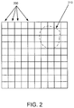
- FIG. 2 shows an example of an EM radiation sensor in accordance with one or more embodiments of the invention.
- the EM radiation sensor ( 130 ) may include a number of sensing regions ( 200 ) that each generate electrical signals in response to EM radiation incident on each region. For example, EM radiation may be incident on a first EM sensing region and a second EM sensing region. The first EM sensing region may produce a first electrical signal and the second EM sensing region may produce a second electrical signal Each of the signals may be proportional to a magnitude and/or frequency of the EM radiation that is incident on each EM sensing region.
- the EM radiation sensor may be a charge-coupled device (CCD).
- CCD charge-coupled device
- the sensing regions ( 200 ) of the EM radiation sensor ( 130 ) may be disposed over a two dimensional area. While the sensing regions ( 200 ) are shown as square regions in a uniform two dimensional grid, the sensing regions ( 200 ) may have other shapes and may be distributed in a uniform or irregular pattern over the surface without departing from the invention. In one or more embodiments of the invention, the two dimensional area may be a flat surface. In one or more embodiments of the invention, the two dimensional area may be a curved surface.
- the EM radiation sensor ( 130 ) may generate electrical signals in response to visible light. In one or more embodiments of the invention, the EM radiation sensor ( 130 ) may generate electrical signals in response to infrared radiation. In one or more embodiments of the invention, the EM radiation sensor ( 130 ) may generate electrical signals in response to ultraviolet light, short-wave infrared light, mid-wave infrared light, long-wave infra-red light, wireless, millimeter wave or terahertz radiation. The EM radiation sensor ( 130 ) may generate electrical signals in response to EM radiation having other spectral content without departing from the invention.
- the system may include one or more masks ( 120 ).
- the masks ( 120 ) may be a physical device that masks portions of the EM radiation sensor ( 130 ) from EM radiation that is incident on the masks ( 120 ).
- the masks ( 120 ) may be disposed between the scene ( 100 ) and the EM radiation sensor ( 130 ) and thereby mask portions of the EM radiation sensor ( 130 ) from EM radiation from the scene ( 100 ).
- the masks ( 120 ) may be disposed at a distance D away from the EM radiation sensor ( 130 ).
- the distance D may be 0.5 mm or less.
- the distance D may be 0 mm, e.g., the masks ( 120 ) may be disposed directly on the EM radiation sensor ( 130 ).
- FIG. 3 shows a diagram of an example of a mask of the masks ( 120 ) in accordance with one or more embodiments of the invention.
- the mask may include a first number of regions ( 300 ) that are opaque and a second number of regions ( 310 ) that are transparent.
- the opaque first number of regions ( 300 ) may prevent the transmission of EM radiation through the mask and the transparent second number of regions ( 310 ) may allow the transmission of EM radiation through the mask.
- opaque first number of regions ( 300 ) may be gold, aluminum, chrome, or other metals.
- the transparent second number of regions ( 310 ) may be glass, quartz, or may be a void space.
- the mask may include a first number of regions ( 300 ) that have refractive indices or thicknesses that are different than the refractive indices and/or thicknesses of a second number of regions ( 310 ) that are transparent.
- the first number of regions ( 300 ) and the second number of regions ( 310 ) may amplitude and/or phase module EM radiation that is transmitted through the mask.
- the first number of regions ( 300 ) and the second number of regions ( 310 ) may be distributed over a two dimensional surface. Each region may be disposed adjacent to other regions. While the first number of regions ( 300 ) and second number of regions ( 310 ) are shown in FIG. 2 in a specific two dimensional pattern, the first number of regions ( 300 ) and second number of regions ( 310 ) may be distributed in other two dimensional patterns or randomly distributed without departing from the invention.
- the first number of regions ( 300 ) and second number of regions ( 310 ) are distributed across the mask in the form of an outer product of two one-dimensional binary sequences.
- Each of the binary sequences may have any values. Values of 1 may indicate an opaque region ( 300 ) while values of 0 may indicate a transparent region ( 310 ), or the reverse.
- the two one dimensional binary sequences are pseudorandom binary sequences.
- the binary sequences are maximum length sequences (M-length sequences).
- the binary sequences are subsets of the Hadamard sequence or the S-matrix sequence.
- the feature size of each opaque region ( 300 ) and each transparent region ( 310 ) may be 10% of the distance between the masks ( 120 ) and the EM radiation sensor ( 130 , FIG. 1 ). In one or more embodiments of the invention, the feature size of each opaque region ( 300 ) and each transparent region ( 310 ) may be 30 ⁇ m.
- each opaque region ( 300 ) and each transparent region ( 310 ) may have a square cross section.
- the square cross section of each region may have an edge length of the feature size of each region.
- a feature size of 30 ⁇ m indicates that each region is a 30 ⁇ m ⁇ 30 ⁇ m square.
- the masks ( 120 ) may be disposed on a transparent support structure.
- the transparent support structure may be, for example, a quartz wafer.
- the system may include one or more illumination sources ( 110 ).
- the illumination sources ( 110 ) may generate EM radiation having at least a portion of a spectral content that is detectable by the EM radiation sensor ( 130 ) and illuminate the scene ( 100 ) with the generated EM radiation.
- the illumination sources ( 110 ) may be, for example, an incandescent source, a light emitting diode, or any other EM radiation producing device. In one or more embodiments of the invention, the illumination sources ( 110 ) may be ambient illumination.
- the system may include an image processor ( 140 ).
- the image processor ( 140 ) may receive the electrical signals generated by the EM radiation sensor ( 130 ) and generate an image of the scene ( 100 ) based on the electrical signals.
- FIG. 4 shows a diagram of an image processor ( 140 ) in accordance with one or more embodiments of the invention.
- the image processor ( 140 ) may be configured to and/or programmed to generate images of a scene ( 100 ) based on electrical signals received from the EM radiation sensor ( 130 ).
- the image processor ( 140 ) may include a processor ( 400 ), transfer function ( 410 ), and storage ( 420 ). Each of the aforementioned components of the system are described below.
- the processor ( 400 ) may be a general purpose processor, embedded processor, programmable gate array, digital signal processor, or any other type of data processing device.
- the storage ( 420 ) may be a non-transitory computer readable storage including instruction that, when executed by the processor ( 400 ), cause the image processor ( 140 ) to perform the functionality shown in FIGS. 5 and 6 , and described below.
- the image processor ( 140 ) may generate an image of the scene ( 100 ) based on a relationship between EM radiation scattered by the scene ( 100 ) and the electrical signals generated by the EM radiation sensor ( 130 ). When EM radiation interacts with the scene ( 100 ), it may be scattered. A portion of the scattered EM radiation may be scattered toward the system as scene EM radiation ( 150 ), as seen in FIG. 1 .
- the masks ( 120 ) may scatter some of the scene EM radiation ( 150 ) as reflected EM radiation ( 160 ) and may scatter some of the scene EM radiation ( 150 ) as transmitted radiation ( 170 ).
- the reflected EM radiation ( 160 ) does not interact with the EM radiation sensor ( 130 ) while the transmitted EM radiation ( 170 ) interacts with the EM radiation sensor ( 130 ), e.g., causes the EM radiation sensor ( 130 ) to generate electrical signals.
- the transmitted EM radiation ( 170 ) may be modulated and diffracted by the masks ( 120 ) when compared to the scene EM radiation ( 150 ). Modulating and diffracting the transmitted EM radiation ( 170 ) may multiplex the transmitted radiation onto a number of sensing regions of the EM radiation sensor.
- a first transparent region ( 320 ) is shown in FIG. 3 .
- a portion of the EM radiation that interacts with the first transparent region ( 320 ) may be scattered onto a number of sensing regions ( 210 ) of the EM radiation sensor as illustrated by the area with a dashed outline shown in FIG. 2 .
- Each of the number of sensing regions ( 210 ) may receive a portion of the EM radiation scattered by the first transparent region ( 320 , FIG. 3 ) and thereby generate electrical signals.
- the scene includes a number of EM radiation sources, e.g., pixels, equal to the number of features of the masks ( 120 ).
- the mask is a 100 ⁇ 100 feature array, it is assumed that the scene consists of 100 ⁇ 100 pixels.
- the incident field is coherent and is represented as a complex-valued field or vector. In one or more embodiments of the invention, the incident field is incoherent and is represented as a real-valued field or vector.
- the image of the scene may be determined by inverting equation (1), assuming the transfer matrix is known.
- the image of the scene may be determined by recording the electrical signals of the EM radiation sensor ( 130 ) when the system is exposed to scene EM radiation ( 150 ).
- Equation (1) may be inverted using any method such as a least-squares problem or other regularized least-squares problem.
- ⁇ L , ⁇ R are sequences that correspond to one-dimensional convolution along the rows and columns of the scene
- X is a matrix of the pixelated image of the scene
- y is a matrix of the electrical signals generated by the EM radiation sensor ( 130 )
- E is the error due to system noise and other factors.
- the transfer matrix may be determined by modeling of the modulation and diffraction of EM radiation due to the masks ( 120 ).
- the masks ( 120 ) may be modeled computationally to determine how light from a scene ( 100 ) is distributed onto the EM radiation sensor and thereby determine the transfer function.
- the transfer matrix may be determined by the method shown in FIG. 5 .
- FIG. 5 shows a flowchart of a method in accordance with one or more embodiments of the invention.
- the method depicted in FIG. 5 may be used to a transfer function of a lens-free imaging device in accordance with one or more embodiments of the invention.
- One or more steps shown in FIG. 5 may be omitted, repeated, and/or performed in a different order among different embodiments.
- a display screen is aligned to the lens-free imaging system.
- the display screen may be, for example, a liquid crystal display. Other types of display may be used without departing from the invention.
- a physical light source such as a point or a line, may be spatially translated to calibrate the transfer matrix.
- the display screen may be aligned to the lens-free imaging system by displaying a test pattern on the display while recording electrical signals from an EM radiation sensor of the lens-free imaging system.
- the display pattern may be, for example, a cross-hairs pattern or point pattern.
- the recorded electrical signals may indicate the degree of alignment between the display and the EM radiation sensor.
- the position of the display and lens-free imaging system may be manually adjusted to improve alignment.
- a first plurality of patterns may be displayed on the display.
- electrical signals generated by the EM radiation sensor may be recorded and stored.
- the plurality of images may be obtained by physically translating a fixed illumination pattern such as a line or a point light source.
- each pattern of the first plurality of patterns displayed may be a unique Hadamard pattern, unique line patterns, or unique dot patterns.
- the number of patterns of the first plurality of patterns may be equal to the number of regions across a width of a mask of the lens-free imaging system.
- Step 520 a second plurality of patterns may be displayed on the display. During the display of each test pattern, electrical signals generated by the EM radiation sensor may be recorded and stored.
- each pattern of the second plurality of patterns displayed may be a unique Hadamard pattern.
- all of the patterns of the first plurality of patterns and second plurality of patterns may be unique Hadamard patterns.
- the number of patterns of the first plurality of patterns may be equal to the number of regions across a height of a mask of the lens-free imaging system.
- a total of 2N patterns may be displayed where N is the number of regions across a width or height of a mask.
- a first one-dimensional convolution sequences and a second one-dimensional convolution sequence are determined.
- the one dimensional convolutions sequences may correspond to the ⁇ L , ⁇ R sequences.
- Step 540 the first one-dimensional convolution sequence and the second one-dimensional convolution sequence are stored.
- Each of the aforementioned stored sequences may be used to calculate a scene image.
- FIG. 6 shows a flowchart of a method in accordance with one or more embodiments of the invention.
- the method depicted in FIG. 6 may be used to generate an image of a scene using a lens-free imaging device in accordance with one or more embodiments of the invention.
- One or more steps shown in FIG. 6 may be omitted, repeated, and/or performed in a different order among different embodiments.
- Step 600 electrical signals from an EM radiation sensor are obtained by an image processor while the EM radiation sensor is exposed to EM radiation from a scene.
- the EM radiation sensor may be exposed to EM radiation for 10 milliseconds.
- Step 610 the image processor generates an image of the scene based the obtained electrical signals and a transfer function.
- the transfer function may be stored in the image processor.
- the transfer function may be a matrix having a number of elements corresponding to the number of regions of a mask of the lens-free imaging system.
- the transfer function may be two one dimensional sequences. Each sequence may have a number of elements corresponding to the number of regions along a width or height of a mask of the lens-free imaging system.
- the least-squares minimization problem may be solved in any way without departing from the invention.
- ⁇ (X) represents a regularizer.
- the regularizer is the total variation, Wavelet sparsity, L1 norm of wavelet, or other patch-based or dictionary-based regularizer.
- the regularizer may be other regularizers without departing from the invention.
- the least-squares minimization problem may be solved in any way without departing from the invention.
- the image of the scene ⁇ circumflex over (X) ⁇ LS may be stored in the image processor and/or displayed and/or stored.
- the image of the scene may be stored in the storage of the image processor.
- embodiments of the invention may include generating a number of images using the above method at different points in time to generate a video.
- an image of a scene at a first point in time may be used to improve the speed of reconstruction of a second image scene at a second point in time. For example, there may be little difference between images of a scene at different points in time that are temporally separated by small amounts, e.g., fractions of a second.
- An image of a scene at a first time that is temporally separated from an image as a scene at a second time may substantially reduce the computation power and time required to solve either equation 4 or equation 5 when compared to generating an image of a scene without a previously generated image of the scene.
- a first example of a lens-free camera system includes a 1036 ⁇ 1048 pixel color EM radiation sensor. Each pixel of the EM radiation sensor may be 6.45 ⁇ m wide. The EM radiation sensor may have a size of 6.7 mm ⁇ 8.9 mm.
- the first example also includes a mask formed from a fused quartz plate with a chrome metallization layer.
- the chrome metallization layer may include a two dimensional patter of opaque regions, e.g., metal areas, and transparent regions, e.g., void regions.
- the pattern of the mask consisted of 510 ⁇ 510 regions. Each region had a feature size of 30 ⁇ m, e.g., square boxes each having an edge length of 30 ⁇ m.
- An outer product of the M-sequence was generated to form a matrix.
- the matrix is shown in FIG. 7B .
- Dark regions indicate a value of 1 while light regions indicate a value of 0.
- the chrome metallization layer on the fused quartz plate was patterned according to the matrix shown in FIG. 7B and thereby formed the mask.
- the mask was placed 0.5 mm away from the color EM radiation sensor. Once formed, images of scenes were taken with an average exposure time of 10 milliseconds. Electrical signals from the EM radiation sensor were recorded while exposed to the scene. Images generated from the scene utilizing the methods shown in FIGS. 5 and 6 . Due to the difference between resolution of the EM radiation sensor and the number of pixels of the mask, the raw data from the EM radiation sensor was sampled to generate electrical signal data corresponding to the same number of pixels of the mask, e.g., 510 ⁇ 510.
- FIGS. 7C-7F show example of images generated by the lens-free camera system. While the images here are shown in black and white, the lens-free camera system generates full color images.
- a second example of a lens-free camera system includes a short wave infrared EM radiation sensor having a resolution of 256 ⁇ 300 pixels. Each pixel of the EM radiation sensor may be 25 ⁇ m wide.
- the second example also includes a mask formed from a fused quartz plate with a chrome metallization layer.
- the chrome metallization layer may include a two dimensional patter of opaque regions, e.g., metal areas, and transparent regions, e.g., void regions.
- the pattern of the mask consisted of 64 ⁇ 64 regions. Each region had a feature size of 100 ⁇ m, e.g., square boxes each having an edge length of 100 ⁇ m.
- a maximum length sequence of length 127 was generated.
- the M-sequence is shown in FIG. 8A .
- the initial pattern was generated with values of either +1 or ⁇ 1.
- values of ⁇ 1 were replaced with values of 0.
- An outer product of the M-sequence was generated to form a matrix.
- the matrix is shown in FIG. 8B .
- Dark regions indicate a value of 1 while light regions indicate a value of 0.
- the chrome metallization layer on the fused quartz plate was patterned according to the matrix shown in FIG. 8B and thereby formed the mask.
- the mask was placed 5 mm away from the color EM radiation sensor. Once formed, images of scenes were taken with an average exposure time of 10 milliseconds. Electrical signals from the EM radiation sensor were recorded while exposed to the scene. Images generated from the scene utilizing the methods shown in FIGS. 5 and 6 . Due to the difference between resolution of the EM radiation sensor and the number of pixels of the mask, the raw data from the EM radiation sensor was sampled to generate electrical signal data corresponding to the same number of pixels of the mask, e.g., 64 ⁇ 64.
- FIGS. 8C-8E show example of images generated by the show wave infrared lens-free camera system. Each image consists of 64 ⁇ 64 pixels.
- One or more embodiments of the invention may provide one or more of the following advantages: (i) A system in accordance with embodiments of the invention may have a thickness-to-width ration of less than 0.1, (ii) the system may have a very high light collection ability, (iii) the system may be much less expensive to produce when compared to an imaging system that integrates a lens, and (iv) the system may be much simpler to produce when compared to lens based imaging systems.
Landscapes
- Engineering & Computer Science (AREA)
- Physics & Mathematics (AREA)
- Signal Processing (AREA)
- Multimedia (AREA)
- Theoretical Computer Science (AREA)
- Computing Systems (AREA)
- General Physics & Mathematics (AREA)
- High Energy & Nuclear Physics (AREA)
- Spectroscopy & Molecular Physics (AREA)
- Molecular Biology (AREA)
- Life Sciences & Earth Sciences (AREA)
- Health & Medical Sciences (AREA)
- Optics & Photonics (AREA)
- Transforming Light Signals Into Electric Signals (AREA)
- Image Processing (AREA)
- Studio Devices (AREA)
Abstract
Description
y=ϕx+e Equation (1)
Y=ϕ L Xϕ R T +E Equation (2)
Y=(ϕL a)(ϕR b)T Equation (3)
{circumflex over (X)} LS=arg minX∥ϕL Xϕ R T −Y∥ 2 2 Equation (4)
{circumflex over (X)} LS=arg minX(∥ϕL Xϕ R T −Y∥ 2 2+θ(X)) Equation (5)
Claims (23)
Priority Applications (1)
| Application Number | Priority Date | Filing Date | Title |
|---|---|---|---|
| US15/547,235 US11178349B2 (en) | 2015-01-29 | 2016-01-29 | Lensless imaging system using an image sensor with one or more attenuating layers |
Applications Claiming Priority (3)
| Application Number | Priority Date | Filing Date | Title |
|---|---|---|---|
| US201562109358P | 2015-01-29 | 2015-01-29 | |
| US15/547,235 US11178349B2 (en) | 2015-01-29 | 2016-01-29 | Lensless imaging system using an image sensor with one or more attenuating layers |
| PCT/US2016/015734 WO2016123529A1 (en) | 2015-01-29 | 2016-01-29 | Lensless imaging system using an image sensor with one or more attenuating layers |
Publications (2)
| Publication Number | Publication Date |
|---|---|
| US20180027201A1 US20180027201A1 (en) | 2018-01-25 |
| US11178349B2 true US11178349B2 (en) | 2021-11-16 |
Family
ID=55808833
Family Applications (1)
| Application Number | Title | Priority Date | Filing Date |
|---|---|---|---|
| US15/547,235 Active US11178349B2 (en) | 2015-01-29 | 2016-01-29 | Lensless imaging system using an image sensor with one or more attenuating layers |
Country Status (5)
| Country | Link |
|---|---|
| US (1) | US11178349B2 (en) |
| EP (1) | EP3251338A1 (en) |
| JP (1) | JP6549240B2 (en) |
| CN (1) | CN107431748A (en) |
| WO (1) | WO2016123529A1 (en) |
Cited By (1)
| Publication number | Priority date | Publication date | Assignee | Title |
|---|---|---|---|---|
| US12401869B1 (en) | 2024-07-11 | 2025-08-26 | Erika Blumenfeld | System and method for imaging an astronomical object from space |
Families Citing this family (33)
| Publication number | Priority date | Publication date | Assignee | Title |
|---|---|---|---|---|
| US20170237918A1 (en) * | 2016-02-12 | 2017-08-17 | The Regents Of The University Of Michigan | Light field imaging with transparent photodetectors |
| EP4016992A3 (en) | 2016-07-13 | 2022-08-24 | Sony Group Corporation | Imaging apparatus, imaging device, and image processing apparatus |
| JP6713549B2 (en) * | 2016-12-27 | 2020-06-24 | 富士フイルム株式会社 | Imaging device and imaging module |
| CN107300827B (en) * | 2017-07-05 | 2020-05-05 | 中国科学院光电研究院 | Low noise lensless imaging method |
| CN111201770B (en) | 2017-10-19 | 2022-08-09 | 索尼公司 | Electronic instrument |
| EP3700197B1 (en) | 2017-10-19 | 2022-11-30 | Sony Group Corporation | Imaging device and method, and image processing device and method |
| US11223787B2 (en) | 2017-10-19 | 2022-01-11 | Sony Corporation | Information processing apparatus, information processing method, and imaging apparatus |
| EP3700192B1 (en) | 2017-10-19 | 2023-08-30 | Sony Group Corporation | Imaging device and signal processing device |
| CN111201780B (en) | 2017-10-19 | 2022-09-16 | 索尼公司 | Imaging apparatus and method, and image processing apparatus and method |
| JPWO2019078337A1 (en) | 2017-10-19 | 2020-12-17 | ソニー株式会社 | Imaging equipment and methods, and image processing equipment and methods |
| US11451715B2 (en) | 2017-10-19 | 2022-09-20 | Sony Corporation | Imaging apparatus, exposure controlling method, and imaging device |
| WO2019078319A1 (en) | 2017-10-19 | 2019-04-25 | ソニー株式会社 | Information processing device, information processing method, imaging device, and program |
| CN111201777B (en) | 2017-10-19 | 2022-02-01 | 索尼公司 | Signal processing apparatus and imaging apparatus |
| WO2019078339A1 (en) | 2017-10-19 | 2019-04-25 | ソニー株式会社 | Electronic apparatus |
| JP7156297B2 (en) | 2017-10-19 | 2022-10-19 | ソニーグループ株式会社 | IMAGE SENSOR, IMAGE PROCESSING DEVICE, IMAGE PROCESSING METHOD, AND PROGRAM |
| JP7322708B2 (en) | 2017-11-30 | 2023-08-08 | ソニーグループ株式会社 | image sensor |
| EP3731521B1 (en) | 2017-12-22 | 2022-04-27 | Sony Group Corporation | Imaging device, imaging method, and imaging element |
| CN111869195B (en) * | 2018-03-14 | 2022-07-08 | 索尼公司 | Image processing apparatus, imaging apparatus, and image processing method |
| WO2019189099A1 (en) | 2018-03-26 | 2019-10-03 | ソニー株式会社 | Image capture element, image capture device, and information processing method |
| CN112106343A (en) | 2018-03-29 | 2020-12-18 | 索尼公司 | Information processing apparatus, information processing method, program, and information processing system |
| CN111989916B (en) | 2018-03-30 | 2022-11-08 | 索尼公司 | Imaging apparatus and method, image processing apparatus and method, and imaging element |
| JP2020067625A (en) * | 2018-10-26 | 2020-04-30 | 国立大学法人九州工業大学 | Optical device |
| WO2020241427A1 (en) | 2019-05-31 | 2020-12-03 | ソニー株式会社 | Imaging device, electronic apparatus, information processing method, and program |
| WO2021041212A1 (en) | 2019-08-23 | 2021-03-04 | The Penn State Research Foundation | Systems and methods for imaging using reconfigurable particle assemblies |
| DE112020006151T5 (en) | 2019-12-16 | 2022-11-03 | Sony Group Corporation | IMAGE FORMING DEVICE, OPTICAL ELEMENT, IMAGE PROCESSING SYSTEM AND IMAGE PROCESSING METHOD |
| CN115315938A (en) | 2020-03-31 | 2022-11-08 | 索尼集团公司 | Image processing apparatus and method, program, and image processing system |
| US11710754B2 (en) * | 2020-09-30 | 2023-07-25 | Visera Technologies Company Limiied | Solid-state image sensor including modulation layer decreasing petal flares |
| US12343954B2 (en) | 2021-04-30 | 2025-07-01 | Industry-Academic Cooperation Foundation, Yonsei University | Apparatus and method for manufacturing phase masks for lens-less camera |
| KR102711130B1 (en) * | 2021-04-30 | 2024-09-27 | 연세대학교 산학협력단 | Phase Mask Design Method and Apparatus for Lensless Camera |
| US12253412B2 (en) * | 2021-05-13 | 2025-03-18 | Viavi Solutions Inc. | Optical sensor device |
| JP2024519198A (en) * | 2021-05-13 | 2024-05-09 | ヴァイアヴィ・ソリューションズ・インコーポレイテッド | Optical Sensor Device |
| US20230221436A1 (en) * | 2022-01-13 | 2023-07-13 | Stmicroelectronics (Research & Development) Limited | Sparse under display lidar |
| EP4701212A1 (en) | 2023-04-21 | 2026-02-25 | Sony Semiconductor Solutions Corporation | Imaging device |
Citations (28)
| Publication number | Priority date | Publication date | Assignee | Title |
|---|---|---|---|---|
| US4991020A (en) | 1989-02-17 | 1991-02-05 | Hughes Aircraft Company | Imaging system for providing separate simultaneous real time images from a singel image sensor |
| US20060157640A1 (en) * | 2005-01-18 | 2006-07-20 | Perlman Stephen G | Apparatus and method for capturing still images and video using coded aperture techniques |
| WO2006125975A1 (en) | 2005-05-23 | 2006-11-30 | Qinetiq Limited | Coded aperture imaging system |
| GB2434934A (en) | 2006-02-06 | 2007-08-08 | Qinetiq Ltd | Processing coded aperture image data by applying weightings to aperture functions and data frames |
| WO2007091051A1 (en) | 2006-02-06 | 2007-08-16 | Qinetiq Limited | Imaging system |
| JP2008527944A (en) | 2005-01-18 | 2008-07-24 | リアデン リミテッド ライアビリティ カンパニー | Apparatus and method for capturing still images and video using coded lens imaging techniques |
| JP2008191661A (en) | 2007-02-06 | 2008-08-21 | Mitsubishi Electric Research Laboratories Inc | Apparatus and method for obtaining 4d light field of scene |
| JP2009522825A (en) | 2006-05-08 | 2009-06-11 | ミツビシ・エレクトリック・リサーチ・ラボラトリーズ・インコーポレイテッド | Method for reducing blur in an image of a scene and method for removing blur in an image of a scene |
| JP2010177918A (en) | 2009-01-28 | 2010-08-12 | Toshiba Corp | Image recording apparatus and manufacturing apparatus of the same |
| US20100321501A1 (en) | 2009-06-23 | 2010-12-23 | Arndt Donald J | Electromagnetic Radiation Detector |
| US20110026141A1 (en) * | 2009-07-29 | 2011-02-03 | Geoffrey Louis Barrows | Low Profile Camera and Vision Sensor |
| US20110085051A1 (en) * | 2009-10-09 | 2011-04-14 | University Of Rochester | Optical element, device, method, and applications |
| US20110204209A1 (en) * | 2009-07-29 | 2011-08-25 | Geoffrey Louis Barrows | Low profile camera and vision sensor |
| JP2012023498A (en) | 2010-07-13 | 2012-02-02 | Fujitsu Ltd | Image processing device and image processing program |
| US20120062760A1 (en) | 2009-03-13 | 2012-03-15 | Ramot At Tel-Aviv University Ltd. | Imaging system and method for imaging objects with reduced image blur |
| US20120268574A1 (en) * | 2011-04-22 | 2012-10-25 | Commissariat A L'energie Atomique Et Aux Ene Alt | Imager integrated circuit and stereoscopic image capture device |
| US20130043375A1 (en) * | 2011-08-15 | 2013-02-21 | Clara BALEINE | Reconfigurable phase change material masks for electro-optical compressive sensing |
| US20130113921A1 (en) * | 2011-11-07 | 2013-05-09 | Raytheon Company | Hadamard enhanced sensors |
| US20140184754A1 (en) * | 2012-12-28 | 2014-07-03 | Samsung Electronics Co., Ltd. | Method of obtaining depth information and display apparatus |
| US20140301535A1 (en) * | 2013-04-05 | 2014-10-09 | The Arizona Board Of Regents On Behalf Of The University Of Arizona | Gamma Ray Imaging Systems And Methods |
| US20150139560A1 (en) * | 2013-11-21 | 2015-05-21 | Bae Systems Information And Electronic Systems Integration Inc. | Coded image system and method thereof |
| US20150215529A1 (en) * | 2014-01-24 | 2015-07-30 | Goodrich Corporation | Random imaging |
| US20150293018A1 (en) * | 2014-04-09 | 2015-10-15 | Rambus Inc. | Low-power image change detector |
| US20150381958A1 (en) * | 2014-02-06 | 2015-12-31 | Bar Ilan University | System and method for imaging with pinhole arrays |
| US20160003994A1 (en) * | 2013-03-05 | 2016-01-07 | Rambus Inc. | Phase gratings with odd symmetry for high-resolution lensless optical sensing |
| US20160065824A1 (en) * | 2014-08-26 | 2016-03-03 | Sensors Unlimited, Inc. | High dynamic range image sensor |
| US20160169667A1 (en) * | 2014-12-11 | 2016-06-16 | Rambus Inc. | Ultra-Miniature Wide-Angle Lensless CMOS Visual Edge Localizer |
| US10753869B2 (en) * | 2016-07-29 | 2020-08-25 | William Marsh Rice University | Lensless imaging device for microscopy and fingerprint biometric |
Family Cites Families (2)
| Publication number | Priority date | Publication date | Assignee | Title |
|---|---|---|---|---|
| CN102130138B (en) * | 2010-01-12 | 2013-01-02 | 中芯国际集成电路制造(上海)有限公司 | Image sensor and forming method thereof |
| JP2011166255A (en) * | 2010-02-05 | 2011-08-25 | Panasonic Corp | Image pickup device |
-
2016
- 2016-01-29 WO PCT/US2016/015734 patent/WO2016123529A1/en not_active Ceased
- 2016-01-29 US US15/547,235 patent/US11178349B2/en active Active
- 2016-01-29 EP EP16718528.9A patent/EP3251338A1/en not_active Ceased
- 2016-01-29 CN CN201680019515.3A patent/CN107431748A/en active Pending
- 2016-01-29 JP JP2017540643A patent/JP6549240B2/en active Active
Patent Citations (31)
| Publication number | Priority date | Publication date | Assignee | Title |
|---|---|---|---|---|
| US4991020A (en) | 1989-02-17 | 1991-02-05 | Hughes Aircraft Company | Imaging system for providing separate simultaneous real time images from a singel image sensor |
| US20060157640A1 (en) * | 2005-01-18 | 2006-07-20 | Perlman Stephen G | Apparatus and method for capturing still images and video using coded aperture techniques |
| JP2008527944A (en) | 2005-01-18 | 2008-07-24 | リアデン リミテッド ライアビリティ カンパニー | Apparatus and method for capturing still images and video using coded lens imaging techniques |
| JP2008542863A (en) | 2005-05-23 | 2008-11-27 | キネテイツク・リミテツド | Coded aperture image system |
| WO2006125975A1 (en) | 2005-05-23 | 2006-11-30 | Qinetiq Limited | Coded aperture imaging system |
| US20090095912A1 (en) * | 2005-05-23 | 2009-04-16 | Slinger Christopher W | Coded aperture imaging system |
| WO2007091051A1 (en) | 2006-02-06 | 2007-08-16 | Qinetiq Limited | Imaging system |
| JP2009529160A (en) | 2006-02-06 | 2009-08-13 | キネテイツク・リミテツド | Imaging system |
| GB2434934A (en) | 2006-02-06 | 2007-08-08 | Qinetiq Ltd | Processing coded aperture image data by applying weightings to aperture functions and data frames |
| JP2009522825A (en) | 2006-05-08 | 2009-06-11 | ミツビシ・エレクトリック・リサーチ・ラボラトリーズ・インコーポレイテッド | Method for reducing blur in an image of a scene and method for removing blur in an image of a scene |
| JP2008191661A (en) | 2007-02-06 | 2008-08-21 | Mitsubishi Electric Research Laboratories Inc | Apparatus and method for obtaining 4d light field of scene |
| JP2010177918A (en) | 2009-01-28 | 2010-08-12 | Toshiba Corp | Image recording apparatus and manufacturing apparatus of the same |
| US20120062760A1 (en) | 2009-03-13 | 2012-03-15 | Ramot At Tel-Aviv University Ltd. | Imaging system and method for imaging objects with reduced image blur |
| US20100321501A1 (en) | 2009-06-23 | 2010-12-23 | Arndt Donald J | Electromagnetic Radiation Detector |
| US20110026141A1 (en) * | 2009-07-29 | 2011-02-03 | Geoffrey Louis Barrows | Low Profile Camera and Vision Sensor |
| US20110204209A1 (en) * | 2009-07-29 | 2011-08-25 | Geoffrey Louis Barrows | Low profile camera and vision sensor |
| US20110085051A1 (en) * | 2009-10-09 | 2011-04-14 | University Of Rochester | Optical element, device, method, and applications |
| JP2012023498A (en) | 2010-07-13 | 2012-02-02 | Fujitsu Ltd | Image processing device and image processing program |
| US20120268574A1 (en) * | 2011-04-22 | 2012-10-25 | Commissariat A L'energie Atomique Et Aux Ene Alt | Imager integrated circuit and stereoscopic image capture device |
| US20130043375A1 (en) * | 2011-08-15 | 2013-02-21 | Clara BALEINE | Reconfigurable phase change material masks for electro-optical compressive sensing |
| US20130113921A1 (en) * | 2011-11-07 | 2013-05-09 | Raytheon Company | Hadamard enhanced sensors |
| US20140184754A1 (en) * | 2012-12-28 | 2014-07-03 | Samsung Electronics Co., Ltd. | Method of obtaining depth information and display apparatus |
| US20160003994A1 (en) * | 2013-03-05 | 2016-01-07 | Rambus Inc. | Phase gratings with odd symmetry for high-resolution lensless optical sensing |
| US20140301535A1 (en) * | 2013-04-05 | 2014-10-09 | The Arizona Board Of Regents On Behalf Of The University Of Arizona | Gamma Ray Imaging Systems And Methods |
| US20150139560A1 (en) * | 2013-11-21 | 2015-05-21 | Bae Systems Information And Electronic Systems Integration Inc. | Coded image system and method thereof |
| US20150215529A1 (en) * | 2014-01-24 | 2015-07-30 | Goodrich Corporation | Random imaging |
| US20150381958A1 (en) * | 2014-02-06 | 2015-12-31 | Bar Ilan University | System and method for imaging with pinhole arrays |
| US20150293018A1 (en) * | 2014-04-09 | 2015-10-15 | Rambus Inc. | Low-power image change detector |
| US20160065824A1 (en) * | 2014-08-26 | 2016-03-03 | Sensors Unlimited, Inc. | High dynamic range image sensor |
| US20160169667A1 (en) * | 2014-12-11 | 2016-06-16 | Rambus Inc. | Ultra-Miniature Wide-Angle Lensless CMOS Visual Edge Localizer |
| US10753869B2 (en) * | 2016-07-29 | 2020-08-25 | William Marsh Rice University | Lensless imaging device for microscopy and fingerprint biometric |
Non-Patent Citations (6)
| Title |
|---|
| Busboom, A. et al.; "Uniformly Redundant Arrays"; Experimental Astronomy, vol. 8, Jun. 1, 1998, pp. 97-123 (27 pages). |
| Cannon, T.M. et al.; "Coded aperture imaging: many holes make light work"; Optical Engineering, vol. 19, No. 3, May 1, 1980, pp. 283-289 (4 pages). |
| First Examination Report issued in corresponding IN Application No. 201727030079 dated Sep. 30, 2019 (5 pages). |
| International Search Report issued in PCT/US2016/015734 dated Jul. 5, 2016 (3 pages). |
| Office Action issued in corresponding Japanese Application No. 2017-540643 dated Jun. 19, 2018, and English translation thereof (31 pages). |
| Written Opinion of the International Searching Authority issued in PCT/US2016/015734 dated Jul. 5, 2016 (8 pages). |
Cited By (1)
| Publication number | Priority date | Publication date | Assignee | Title |
|---|---|---|---|---|
| US12401869B1 (en) | 2024-07-11 | 2025-08-26 | Erika Blumenfeld | System and method for imaging an astronomical object from space |
Also Published As
| Publication number | Publication date |
|---|---|
| WO2016123529A1 (en) | 2016-08-04 |
| CN107431748A (en) | 2017-12-01 |
| EP3251338A1 (en) | 2017-12-06 |
| JP6549240B2 (en) | 2019-07-24 |
| JP2018505617A (en) | 2018-02-22 |
| US20180027201A1 (en) | 2018-01-25 |
Similar Documents
| Publication | Publication Date | Title |
|---|---|---|
| US11178349B2 (en) | Lensless imaging system using an image sensor with one or more attenuating layers | |
| Tajima et al. | Lensless light-field imaging with multi-phased fresnel zone aperture | |
| DeWeert et al. | Lensless coded-aperture imaging with separable Doubly-Toeplitz masks | |
| EP3157410B1 (en) | System for lensed and lensless optical sensing | |
| CN110692233B (en) | Image pickup device, image processing device, image pickup system, image processing method, and recording medium | |
| Stork et al. | Optical, mathematical, and computational foundations of lensless ultra-miniature diffractive imagers and sensors | |
| Evtikhiev et al. | Measurement of noises and modulation transfer function of cameras used in optical-digital correlators | |
| CN106104318A (en) | Low Power Image Change Detector | |
| US11460666B2 (en) | Imaging apparatus and method, and image processing apparatus and method | |
| CN102192781A (en) | An apparatus and a method for performing a difference measurement of an object image | |
| JPWO2019171691A1 (en) | Image processing device, imaging device, and image processing method | |
| CN108873565A (en) | Photographic device | |
| Wecksung et al. | Digital image processing at EG&G | |
| JP2023016864A (en) | Imaging device and method | |
| EP3440624A1 (en) | Computational imaging with uncalibrated pupil phase | |
| WO2023230412A1 (en) | Class-specific diffractive camera with all-optical erasure of undesired objects | |
| Naranjo et al. | Experimental demonstration of multi-spectral imaging of vegetation with a diffractive plenoptic camera | |
| JP7159118B2 (en) | Imaging device | |
| O’Neill et al. | Portable COTS RGB wavefront sensor | |
| US20250305880A1 (en) | Light detection apparatus, light detection system, and filter array | |
| US20250317634A1 (en) | Multispectral image sensor, camera system and method of manufacturing a multispectral image sensor | |
| Starikov et al. | Using commercial photo camera’s RAW-based images in optical-digital correlator for pattern recognition | |
| Borcoski et al. | Multispectral LWIR plenoptics system free of FPN | |
| CN120044648A (en) | Pixel polaroid array, design method thereof and polarization imaging device | |
| ŘÍČNÝ et al. | Analysis of Resolution in Aerial Earth Surface Photography |
Legal Events
| Date | Code | Title | Description |
|---|---|---|---|
| FEPP | Fee payment procedure |
Free format text: ENTITY STATUS SET TO SMALL (ORIGINAL EVENT CODE: SMAL); ENTITY STATUS OF PATENT OWNER: SMALL ENTITY |
|
| AS | Assignment |
Owner name: WILLIAM MARSH RICE UNIVERSITY, TEXAS Free format text: ASSIGNMENT OF ASSIGNORS INTEREST;ASSIGNORS:SANKARANARAYANAN, ASWIN;VEERARAGHAVAN, ASHOK;HENDRICKS, LISA A.;AND OTHERS;SIGNING DATES FROM 20170805 TO 20171024;REEL/FRAME:043958/0816 |
|
| STPP | Information on status: patent application and granting procedure in general |
Free format text: NON FINAL ACTION MAILED |
|
| STPP | Information on status: patent application and granting procedure in general |
Free format text: RESPONSE TO NON-FINAL OFFICE ACTION ENTERED AND FORWARDED TO EXAMINER |
|
| STPP | Information on status: patent application and granting procedure in general |
Free format text: FINAL REJECTION MAILED |
|
| STPP | Information on status: patent application and granting procedure in general |
Free format text: DOCKETED NEW CASE - READY FOR EXAMINATION |
|
| STPP | Information on status: patent application and granting procedure in general |
Free format text: FINAL REJECTION MAILED |
|
| STPP | Information on status: patent application and granting procedure in general |
Free format text: RESPONSE AFTER FINAL ACTION FORWARDED TO EXAMINER |
|
| STPP | Information on status: patent application and granting procedure in general |
Free format text: ADVISORY ACTION MAILED |
|
| STPP | Information on status: patent application and granting procedure in general |
Free format text: DOCKETED NEW CASE - READY FOR EXAMINATION |
|
| STPP | Information on status: patent application and granting procedure in general |
Free format text: NOTICE OF ALLOWANCE MAILED -- APPLICATION RECEIVED IN OFFICE OF PUBLICATIONS |
|
| STPP | Information on status: patent application and granting procedure in general |
Free format text: PUBLICATIONS -- ISSUE FEE PAYMENT VERIFIED |
|
| STCF | Information on status: patent grant |
Free format text: PATENTED CASE |
|
| MAFP | Maintenance fee payment |
Free format text: PAYMENT OF MAINTENANCE FEE, 4TH YR, SMALL ENTITY (ORIGINAL EVENT CODE: M2551); ENTITY STATUS OF PATENT OWNER: SMALL ENTITY Year of fee payment: 4 |