US11171187B2 - Display device and manufacturing method thereof - Google Patents
Display device and manufacturing method thereof Download PDFInfo
- Publication number
- US11171187B2 US11171187B2 US16/103,821 US201816103821A US11171187B2 US 11171187 B2 US11171187 B2 US 11171187B2 US 201816103821 A US201816103821 A US 201816103821A US 11171187 B2 US11171187 B2 US 11171187B2
- Authority
- US
- United States
- Prior art keywords
- layer
- barrier
- electrode
- fluorine
- display device
- Prior art date
- Legal status (The legal status is an assumption and is not a legal conclusion. Google has not performed a legal analysis and makes no representation as to the accuracy of the status listed.)
- Active, expires
Links
- 238000004519 manufacturing process Methods 0.000 title description 14
- 230000004888 barrier function Effects 0.000 claims abstract description 124
- 239000000758 substrate Substances 0.000 claims abstract description 40
- 239000010409 thin film Substances 0.000 claims abstract description 26
- 239000000463 material Substances 0.000 claims description 76
- 239000011737 fluorine Substances 0.000 claims description 34
- 229910052731 fluorine Inorganic materials 0.000 claims description 34
- 229920002120 photoresistant polymer Polymers 0.000 claims description 12
- PXGOKWXKJXAPGV-UHFFFAOYSA-N Fluorine Chemical compound FF PXGOKWXKJXAPGV-UHFFFAOYSA-N 0.000 claims 1
- 239000010410 layer Substances 0.000 description 229
- 238000000034 method Methods 0.000 description 38
- YCKRFDGAMUMZLT-UHFFFAOYSA-N Fluorine atom Chemical compound [F] YCKRFDGAMUMZLT-UHFFFAOYSA-N 0.000 description 33
- 230000008569 process Effects 0.000 description 25
- 238000009832 plasma treatment Methods 0.000 description 19
- 238000002347 injection Methods 0.000 description 16
- 239000007924 injection Substances 0.000 description 16
- 239000003990 capacitor Substances 0.000 description 12
- 238000009413 insulation Methods 0.000 description 12
- 239000004065 semiconductor Substances 0.000 description 11
- 238000010438 heat treatment Methods 0.000 description 8
- 230000005525 hole transport Effects 0.000 description 7
- 239000011229 interlayer Substances 0.000 description 7
- 239000011248 coating agent Substances 0.000 description 6
- 238000000576 coating method Methods 0.000 description 6
- 230000002209 hydrophobic effect Effects 0.000 description 5
- VYPSYNLAJGMNEJ-UHFFFAOYSA-N silicon dioxide Inorganic materials O=[Si]=O VYPSYNLAJGMNEJ-UHFFFAOYSA-N 0.000 description 5
- 229910052814 silicon oxide Inorganic materials 0.000 description 4
- 229910052581 Si3N4 Inorganic materials 0.000 description 3
- HQVNEWCFYHHQES-UHFFFAOYSA-N silicon nitride Chemical compound N12[Si]34N5[Si]62N3[Si]51N64 HQVNEWCFYHHQES-UHFFFAOYSA-N 0.000 description 3
- 238000007641 inkjet printing Methods 0.000 description 2
- 239000002356 single layer Substances 0.000 description 2
- 239000004642 Polyimide Substances 0.000 description 1
- 229910004205 SiNX Inorganic materials 0.000 description 1
- XUIMIQQOPSSXEZ-UHFFFAOYSA-N Silicon Chemical compound [Si] XUIMIQQOPSSXEZ-UHFFFAOYSA-N 0.000 description 1
- 229910021417 amorphous silicon Inorganic materials 0.000 description 1
- 230000008901 benefit Effects 0.000 description 1
- 239000000919 ceramic Substances 0.000 description 1
- 230000008878 coupling Effects 0.000 description 1
- 238000010168 coupling process Methods 0.000 description 1
- 238000005859 coupling reaction Methods 0.000 description 1
- 230000000694 effects Effects 0.000 description 1
- 230000007613 environmental effect Effects 0.000 description 1
- 230000005281 excited state Effects 0.000 description 1
- 230000007717 exclusion Effects 0.000 description 1
- 239000010408 film Substances 0.000 description 1
- 239000011521 glass Substances 0.000 description 1
- 230000005283 ground state Effects 0.000 description 1
- 239000007788 liquid Substances 0.000 description 1
- 239000011159 matrix material Substances 0.000 description 1
- 238000012986 modification Methods 0.000 description 1
- 230000004048 modification Effects 0.000 description 1
- 239000011368 organic material Substances 0.000 description 1
- 239000004033 plastic Substances 0.000 description 1
- 229910021420 polycrystalline silicon Inorganic materials 0.000 description 1
- 229920001721 polyimide Polymers 0.000 description 1
- 229920005591 polysilicon Polymers 0.000 description 1
- 238000007639 printing Methods 0.000 description 1
- 239000002096 quantum dot Substances 0.000 description 1
- 239000010453 quartz Substances 0.000 description 1
- 229910052710 silicon Inorganic materials 0.000 description 1
- 239000010703 silicon Substances 0.000 description 1
- 239000002904 solvent Substances 0.000 description 1
Images


Classifications
-
- H—ELECTRICITY
- H10—SEMICONDUCTOR DEVICES; ELECTRIC SOLID-STATE DEVICES NOT OTHERWISE PROVIDED FOR
- H10K—ORGANIC ELECTRIC SOLID-STATE DEVICES
- H10K50/00—Organic light-emitting devices
- H10K50/80—Constructional details
- H10K50/84—Passivation; Containers; Encapsulations
-
- H01L27/3246—
-
- H—ELECTRICITY
- H10—SEMICONDUCTOR DEVICES; ELECTRIC SOLID-STATE DEVICES NOT OTHERWISE PROVIDED FOR
- H10K—ORGANIC ELECTRIC SOLID-STATE DEVICES
- H10K59/00—Integrated devices, or assemblies of multiple devices, comprising at least one organic light-emitting element covered by group H10K50/00
- H10K59/10—OLED displays
- H10K59/12—Active-matrix OLED [AMOLED] displays
- H10K59/122—Pixel-defining structures or layers, e.g. banks
-
- H01L51/0005—
-
- H01L51/0012—
-
- H—ELECTRICITY
- H10—SEMICONDUCTOR DEVICES; ELECTRIC SOLID-STATE DEVICES NOT OTHERWISE PROVIDED FOR
- H10K—ORGANIC ELECTRIC SOLID-STATE DEVICES
- H10K50/00—Organic light-emitting devices
- H10K50/80—Constructional details
- H10K50/805—Electrodes
-
- H—ELECTRICITY
- H10—SEMICONDUCTOR DEVICES; ELECTRIC SOLID-STATE DEVICES NOT OTHERWISE PROVIDED FOR
- H10K—ORGANIC ELECTRIC SOLID-STATE DEVICES
- H10K59/00—Integrated devices, or assemblies of multiple devices, comprising at least one organic light-emitting element covered by group H10K50/00
- H10K59/10—OLED displays
- H10K59/12—Active-matrix OLED [AMOLED] displays
- H10K59/121—Active-matrix OLED [AMOLED] displays characterised by the geometry or disposition of pixel elements
- H10K59/1213—Active-matrix OLED [AMOLED] displays characterised by the geometry or disposition of pixel elements the pixel elements being TFTs
-
- H—ELECTRICITY
- H10—SEMICONDUCTOR DEVICES; ELECTRIC SOLID-STATE DEVICES NOT OTHERWISE PROVIDED FOR
- H10K—ORGANIC ELECTRIC SOLID-STATE DEVICES
- H10K71/00—Manufacture or treatment specially adapted for the organic devices covered by this subclass
- H10K71/10—Deposition of organic active material
- H10K71/12—Deposition of organic active material using liquid deposition, e.g. spin coating
- H10K71/13—Deposition of organic active material using liquid deposition, e.g. spin coating using printing techniques, e.g. ink-jet printing or screen printing
- H10K71/135—Deposition of organic active material using liquid deposition, e.g. spin coating using printing techniques, e.g. ink-jet printing or screen printing using ink-jet printing
-
- H—ELECTRICITY
- H10—SEMICONDUCTOR DEVICES; ELECTRIC SOLID-STATE DEVICES NOT OTHERWISE PROVIDED FOR
- H10K—ORGANIC ELECTRIC SOLID-STATE DEVICES
- H10K71/00—Manufacture or treatment specially adapted for the organic devices covered by this subclass
- H10K71/10—Deposition of organic active material
- H10K71/191—Deposition of organic active material characterised by provisions for the orientation or alignment of the layer to be deposited
-
- H01L2227/323—
-
- H01L2251/558—
-
- H01L51/5012—
-
- H01L51/5056—
-
- H01L51/5072—
-
- H01L51/5088—
-
- H01L51/5092—
-
- H—ELECTRICITY
- H10—SEMICONDUCTOR DEVICES; ELECTRIC SOLID-STATE DEVICES NOT OTHERWISE PROVIDED FOR
- H10K—ORGANIC ELECTRIC SOLID-STATE DEVICES
- H10K2102/00—Constructional details relating to the organic devices covered by this subclass
- H10K2102/301—Details of OLEDs
- H10K2102/351—Thickness
-
- H—ELECTRICITY
- H10—SEMICONDUCTOR DEVICES; ELECTRIC SOLID-STATE DEVICES NOT OTHERWISE PROVIDED FOR
- H10K—ORGANIC ELECTRIC SOLID-STATE DEVICES
- H10K50/00—Organic light-emitting devices
- H10K50/10—OLEDs or polymer light-emitting diodes [PLED]
- H10K50/11—OLEDs or polymer light-emitting diodes [PLED] characterised by the electroluminescent [EL] layers
-
- H—ELECTRICITY
- H10—SEMICONDUCTOR DEVICES; ELECTRIC SOLID-STATE DEVICES NOT OTHERWISE PROVIDED FOR
- H10K—ORGANIC ELECTRIC SOLID-STATE DEVICES
- H10K50/00—Organic light-emitting devices
- H10K50/10—OLEDs or polymer light-emitting diodes [PLED]
- H10K50/14—Carrier transporting layers
- H10K50/15—Hole transporting layers
-
- H—ELECTRICITY
- H10—SEMICONDUCTOR DEVICES; ELECTRIC SOLID-STATE DEVICES NOT OTHERWISE PROVIDED FOR
- H10K—ORGANIC ELECTRIC SOLID-STATE DEVICES
- H10K50/00—Organic light-emitting devices
- H10K50/10—OLEDs or polymer light-emitting diodes [PLED]
- H10K50/14—Carrier transporting layers
- H10K50/16—Electron transporting layers
-
- H—ELECTRICITY
- H10—SEMICONDUCTOR DEVICES; ELECTRIC SOLID-STATE DEVICES NOT OTHERWISE PROVIDED FOR
- H10K—ORGANIC ELECTRIC SOLID-STATE DEVICES
- H10K50/00—Organic light-emitting devices
- H10K50/10—OLEDs or polymer light-emitting diodes [PLED]
- H10K50/17—Carrier injection layers
-
- H—ELECTRICITY
- H10—SEMICONDUCTOR DEVICES; ELECTRIC SOLID-STATE DEVICES NOT OTHERWISE PROVIDED FOR
- H10K—ORGANIC ELECTRIC SOLID-STATE DEVICES
- H10K50/00—Organic light-emitting devices
- H10K50/10—OLEDs or polymer light-emitting diodes [PLED]
- H10K50/17—Carrier injection layers
- H10K50/171—Electron injection layers
-
- H—ELECTRICITY
- H10—SEMICONDUCTOR DEVICES; ELECTRIC SOLID-STATE DEVICES NOT OTHERWISE PROVIDED FOR
- H10K—ORGANIC ELECTRIC SOLID-STATE DEVICES
- H10K59/00—Integrated devices, or assemblies of multiple devices, comprising at least one organic light-emitting element covered by group H10K50/00
- H10K59/10—OLED displays
- H10K59/12—Active-matrix OLED [AMOLED] displays
- H10K59/1201—Manufacture or treatment
Definitions
- the technical field relates to a display device and a method for manufacturing the display device.
- An inkjet printing device may discharge fine droplets at one or more locations on a printing medium.
- An inkjet printing device may be used in manufacturing a display device.
- Embodiments may be related to a display device that includes a light emitting element layer of satisfactory quality. Embodiments may be related to a method for manufacturing the display device.
- a display device includes the following elements: a substrate; a thin film transistor that is disposed on the substrate; a first electrode that is connected with the thin film transistor; a second electrode that overlaps the first electrode; and a barrier that is disposed between the first electrode and the second electrode, wherein the barrier includes an opening that overlaps the first electrode, an upper surface of the barrier is fluorine-doped, and a side surface of an opening of the barrier is hydrophilic.
- a thickness of the fluorine-doped area of the barrier may be about 10 nm to about 100 nm.
- a ratio of the thickness of the fluorine-doped area of the barrier with respect to the entire thickness of the barrier may be about 0.05% to about 20%.
- the barrier may include a first barrier and a second barrier that are sequentially stacked, the second barrier may be disposed closer to the second electrode than the first barrier, and an area of the second barrier, adjacent to the second electrode, may be fluorine-doped.
- the first barrier and the second barrier may include the same material.
- the first barrier and the second barrier may include different materials.
- a method for manufacturing a display device includes the following steps: preparing a substrate that includes a thin film transistor and a first electrode connected to the thin film transistor; forming a second layer including fluorine on the substrate and a first layer disposed on the second layer; forming an opening that overlaps the first electrode by exposing and developing the second layer and the first layer; and removing the first layer by performing plasma treatment on the opening, the second layer, and the first layer.
- a thickness of an area of the second layer, including fluorine, may be about 10 nm to about 100 nm.
- a thickness of the first layer may be reduced.
- a side surface of the opening may have hydrophilicity.
- the plasma treatment may be carried out by using at least one of O 2 , Ar, N 2 , NF 3 , and CF 4
- the first layer and the first layer may include the same material, and the second layer may further include fluorine in addition to the material of the first layer.
- the second layer and the first layer may include different materials.
- the method may further include, in the forming of the second layer including fluorine on the substrate and the first layer disposed on the second layer, forming a third layer between the second layer and the first layer.
- the third layer, the second layer, and the first layer may be formed on the substrate through coating and heating a material of the third layer, coating and heating a material of the second layer, and coating and heating a material of the first layer.
- the first layer and the third layer may include the same material.
- the method may further include forming at least one of an electron injection layer (EIL), an electron transport layer (ETL), an emission layer, a hole transport layer (HTL), and a hole injection layer (HIL) in the opening, through an inkjet process.
- EIL electron injection layer
- ETL electron transport layer
- HTL hole transport layer
- HIL hole injection layer
- An embodiment may be related to a display device.
- the display device may include a substrate, a thin film transistor, a first electrode, a second electrode, and a barrier.
- the thin film transistor may be disposed on the substrate.
- the first electrode may be electrically connected to the thin film transistor.
- the second electrode overlaps the first electrode.
- the barrier has a first portion and a second portion.
- the second portion may be disposed between the first portion and the second electrode and may be fluorine-doped.
- a side surface of the first portion may be part of a boundary of an opening of the barrier and may be hydrophilic.
- the opening of the barrier may be disposed between the first electrode and the second electrode.
- a thickness of the second portion in a direction perpendicular to the substrate may be in a range of 10 nm to 100 nm.
- the first portion may not be fluorine-doped.
- a ratio of a thickness of the second portion in a direction perpendicular to the substrate with respect to a thickness of the barrier in the direction perpendicular to the substrate may be in a range of 0.05% to 20%.
- a face of the second portion may directly contact the second electrode and may be fluorine-doped.
- the first portion and the second potion may include a same material.
- the first portion may include a first material.
- the second portion may include a second material different from each of fluorine and the first material.
- An embodiment may be related to a method for manufacturing a display device.
- the method may include the following steps: preparing a substrate that includes a thin film transistor and a first electrode electrically connected to the thin film transistor; forming a material layer on the substrate, wherein the material layer may include a fluorine-containing portion; forming a cover layer on the second layer; forming an opening that exposes the first electrode by partially removing the cover layer and the material layer; and removing remaining portions of the cover layer by performing plasma treatment.
- a thickness of the fluorine-containing portion in a direction perpendicular to the substrate may be in a range of 10 nm to 100 nm.
- a thickness of the cover layer in a direction perpendicular to the substrate may be reduced.
- a surface of a remaining portion of the material layer may surround the opening and may have hydrophilicity.
- Plasma used in the plasma treatment may include at least one of O 2 , Ar, N 2 , NF 3 , and CF 4 .
- Both the material layer and the cover layer may include a first material.
- the material layer further may include fluorine in addition to the first material.
- the material layer may include a first material and fluorine.
- the cover layer may include a non-fluorine material different from the first material.
- the method may include forming an intermediate layer between the material layer and the substrate.
- the intermediate layer, the material layer, and the cover layer may be formed on the substrate through coating and heating a material of the intermediate layer, subsequently coating and heating a material of the material layer, and subsequently coating and heating a material of the cover layer.
- the cover layer and the intermediate layer may include a same material.
- the method may include forming at least one of an electron injection layer (EIL), an electron transport layer (ETL), an emission layer, a hole transport layer (HTL), and a hole injection layer (HIL) in the opening, through an inkjet process.
- EIL electron injection layer
- ETL electron transport layer
- HTL hole transport layer
- HIL hole injection layer
- a display device that can effectively form a light emitting element layer using an inkjet process, and a manufacturing method thereof can be provided.
- FIG. 1 schematically shows a cross-sectional view of a display device according to an embodiment.
- FIG. 2 shows a configuration (or a schematic cross-sectional view) in which an inkjet material stays within a barrier having hydrophobicity rather than overflowing due to the hydrophobicity of the barrier according to an embodiment.
- FIG. 3 is an image illustrating that an inkjet material overflows since a barrier does not have hydrophobicity according to an embodiment.
- FIG. 4 is an image illustrating that an inkjet material is not sufficiently spread because the barrier is hydrophobic up to a side wall according to an embodiment.
- FIG. 5 shows a schematic cross-sectional view of a display device according to an embodiment.
- FIG. 6 is a schematic top plan view of a display device according to an embodiment.
- FIG. 7 is a cross-sectional view of the display device illustrated in FIG. 6 , taken along the line VII-VII′, according to an embodiment.
- FIG. 8 , FIG. 9 , FIG. 10 , FIG. 11 , FIG. 12 , and FIG. 13 are schematic cross-sectional views of structures formed in a method for manufacturing a light emitting element of a display device according to an embodiment.
- FIG. 14 , FIG. 15 , and FIG. 16 are schematic cross-sectional views of structures formed in a method for manufacturing a display device according to an embodiment.
- first,” “second,” etc. may be used herein to describe various elements, these elements, should not be limited by these terms. These terms may be used to distinguish one element from another element. Thus, a first element may be termed a second element without departing from teachings of one or more embodiments. The description of an element as a “first” element may not require or imply the presence of a second element or other elements.
- the terms “first,” “second,” etc. may also be used herein to differentiate different categories or sets of elements. For conciseness, the terms “first,” “second,” etc. may represent “first-type (or first-set),” “second-type (or second-set),” etc., respectively.
- first element When a first element is referred to as being “on” a second element, the first element can be directly on the second element, or one or more intervening elements may be present between the first element and the second element. When a first element is referred to as being “directly on” a second element, there are no intended intervening elements (except environmental elements such as air) provided between the first element and the second element.
- the word “on” or “above” means positioned on or below an object, and does not necessarily mean positioned on the upper side of the object based on a gravitational direction.
- connection may mean “electrically connect”; the term “insulate” may mean “electrically insulate”; the term “area” may mean “portion.”
- FIG. 1 and FIG. 7 schematically illustrate a display device according to an embodiment.
- a light emitting display device includes a substrate 110 , a thin film transistor TFT disposed on the substrate 110 , a first electrode 191 connected with the thin film transistor TFT, a second electrode 270 overlapping the first electrode 191 , a barrier 380 and a light emitting layer 370 that are disposed between the first electrode 191 and the second electrode 270 , and an insulation layer 180 disposed between the thin film transistor TFT and the first electrode 191 .
- the barrier 380 includes a first barrier 381 and a second barrier 382 , and fluorine is included in an area/portion of the second barrier 382 where the second barrier 382 and the second electrode 270 are adjacent to each other.
- the area/portion where fluorine is included in the second barrier 382 is an upper area, and a side area of an opening B of the barrier 380 (or of the second barrier 382 and/or first barrier 381 ) is not doped with fluorine.
- the barrier 380 may have a thickness in a range of about 0.5 ⁇ m to about 2 ⁇ m in a direction perpendicular to the substrate 110 .
- the area doped with fluorine may have a thickness in a range of about 10 nm to about 100 nm in the direction perpendicular to the substrate 110 .
- a ratio of the area/portion doped with fluorine with respect to the thickness of the whole barrier may be in a range of about 0.05% to about 20%.
- the first barrier 381 and the second barrier 382 may include the same material or may include different materials.
- the first barrier 381 and the second barrier 382 may include negative photoresists.
- a hole injection layer, a hole transport layer, an emission layer, an electron transport layer, and an electron injection layer included in the light emitting layer 370 in the display device may be formed through one or more inkjet processes.
- an upper surface of the barrier 380 needs to be hydrophobic.
- FIG. 2 shows a configuration in which an inkjet material 371 stays only in the opening of the barrier 380 due to hydrophobicity of the barrier 380 .
- the upper surface of the barrier 380 needs to be hydrophobic in order to form the light emitting layer only in the opening of the barrier 380 during an inkjet process.
- the inkjet material 371 cannot be sufficiently spread in the opening of the barrier 380 .
- FIG. 3 is an image showing that an inkjet material overflows because the upper surface of the barrier does not have (sufficient) hydrophobicity
- FIG. 4 is an image showing that an inkjet material does not sufficiently spread because the side surface of the barrier has (too much) hydrophobicity.
- the barrier needs to have proper hydrophobic and/or hydrophilic characteristics in order to make a material spread well and prevent overflowing.
- the barrier 380 may include a double-layer structure, and an upper area/portion of the second barrier 382 disposed above has hydrophobicity because the upper area is doped with fluorine and side surfaces of the first and second barriers 381 and 281 may have hydrophilicity because they are not doped with fluorine may define one or more boundaries of the opening B.
- the barrier 380 has hydrophilicity within the opening B, and the upper area, which is the outside the opening B, has hydrophobicity.
- the layers included in the light emitting element layer 370 are manufactured through one or more inkjet processes in the opening B of the barrier 380 , an inkjet material spreads well in the opening B due to hydrophilicity of the side surfaces of the barrier 380 . Since the upper surface of the barrier 380 has hydrophobicity because of being doped with fluorine, the inkjet material can be prevented from overflowing. Accordingly, the light emitting element layer 370 can be effectively manufactured through the one or more inkjet processes.
- FIG. 1 and FIG. 7 illustrate that the barrier 380 includes the first barrier 381 and the second barrier 382 , but the barrier 380 may not include both layers 381 and 382 .
- the barrier 380 can provide the same effect if an upper surface of the barrier 380 has hydrophobicity by being fluorine-doped and a side surface of an opening has hydrophilicity.
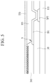
- FIG. 5 shows a display device according to an embodiment. Referring to FIG. 5 , the barrier 380 is provided as a single layer with a fluorine-doped top portion.
- a thickness of the fluorine-doped top portion may be in a range of about 0.05% to about 20% with respect to a thickness of the entire barrier 380 in a direction perpendicular to the substrate 110 and may have sufficient hydrophobicity.
- a side surface of the barrier 380 that defines a boundary of an opening B has hydrophilicity.
- FIG. 6 is a schematic top plan view of a display device according to an embodiment.
- FIG. 7 is a cross-sectional view of FIG. 6 , taken along the line VII-VII′.
- an active matrix (AM) type of light emitting display is illustrated to have a 2Tr-1Cap structure in which two transistors (TFTs) and one capacitor are provided for each pixel of a display area.
- each pixel in the light emitting display device, may be provided with three or more transistors and two or more capacitors, and may be formed to have various structures by further forming additional wires.
- the pixel is a minimum unit for displaying an image, and the display area displays the image through the plurality of pixels.
- the light emitting display device includes a switching thin film transistor T 1 , a driving thin film transistor T 2 , a capacitor C 1 , and a light emitting element E 1 , which are formed in each of the plurality of pixels on the substrate 110 .
- each pixel may be defined by the boundary of the gate line 121 , the data line 171 , and the common power line 172 , but this is not restrictive.
- the organic light emitting element E 1 includes the first electrode 191 , the light emitting element layer 370 disposed on the first electrode 191 , and the second electrode 270 disposed on the light emitting element layer 370 .
- the first electrode 191 is a positive electrode, which is a hole injection electrode
- the second electrode 270 is a negative electrode, which is an electron injection electrode
- the first electrode 191 may be a negative electrode and the second electrode 270 may be a positive electrode depending on a driving method of the light emitting display device.
- the first electrode 191 may be a pixel electrode and the second electrode 270 may be a common electrode.
- the light emitting element layer 370 may include at least one of a hole injection layer (HIL), a hole transport layer (HTL), an emission layer, an electron transport layer (ETL), and an electron injection layer (EIL).
- HIL hole injection layer
- HTL hole transport layer
- ETL electron transport layer
- EIL electron injection layer
- the emission layer may include an organic emission layer, and an exciton generated by coupling injected holes and electrons falls from an excited state to a ground state to emit light.
- the emission layer may include quantum dots.
- the capacitor C 1 includes a pair of capacitor plates 158 and 178 and an interlayer insulating layer 160 interposed between the plates 158 and 178 .
- the interlayer insulating layer 160 functions as a dielectric member. Capacitance is determined by charges charged in the capacitor C 1 and a voltage between the pair of capacitor plates 158 and 178 .
- the switching thin film transistor T 1 includes a switching semiconductor layer 151 , a switching gate electrode 122 , a switching source electrode 176 , and a switching drain electrode 177 .
- the driving thin film transistor T 2 includes a driving semiconductor layer 155 , a driving gate electrode 124 , a driving source electrode 173 , and a driving drain electrode 175 .
- the switching thin film transistor T 1 is used as a switch to select a pixel for light emission.
- the switching gate electrode 122 is connected with the gate line 121 and the switching source electrode 176 is connected with the data line 171 .
- the switching drain electrode 177 is disposed apart from the switching source electrode 176 , while being connected with one (e.g., 158 ) of the pair of capacitor plates 158 and 178 .
- the driving thin film transistor T 2 applies driving power to the first electrode 191 for light emission of the light emitting element layer 370 of the organic light emitting element E 1 in the selected pixel.
- the driving gate electrode 124 is connected with the capacitor plate 158 to which the switching drain electrode 177 is connected.
- the driving source electrode 173 and the other capacitor plate 178 are respectively connected to the common power line 172 .
- the driving drain electrode 175 is connected to the first electrode 191 through a contact hole 185 .
- a buffer layer 111 is disposed on the substrate 110 .
- the substrate 110 may be made of at least one of glass, quartz, ceramic, plastic, and the like.
- the buffer layer 111 may be made of at least one of a silicon nitride (SiNx), a silicon oxide (SiO x ), a silicon oxynitride (SiOxNy), and the like.
- SiNx silicon nitride
- SiO x silicon oxide
- SiOxNy silicon oxynitride
- x and y may respectively be in a range of 1 to 5.
- the driving semiconductor layer 155 is disposed on the buffer layer 111 .
- the driving semiconductor layer 155 may be made of at least one of various semiconductor materials such as a polysilicon layer, an amorphous silicon layer, and the like.
- the driving semiconductor layer 155 may include a source region 152 , a channel region 153 , and a drain region 154 .
- a gate insulation layer 140 that is made of a silicon nitride or a silicon oxide is disposed on the driving semiconductor layer 155 .
- the driving gate electrode 124 and the first capacitor plate 158 are disposed on the gate insulation layer 140 .
- the driving gate electrode 124 overlaps at least a part of the driving semiconductor 155 , and specifically, the channel area 153 of the driving semiconductor 155 .
- the interlayer insulation layer 160 that covers the driving gate electrode 124 is disposed on the gate insulation layer 140 .
- the interlayer insulating layer 160 may be made of a silicon nitride or a silicon oxide.
- the gate insulation layer 140 and the interlayer insulating layer 160 include a first contact hole 163 and a second contact hole 165 that expose the source area 153 and the drain area 154 of the driving semiconductor layer 155 .
- the driving source electrode 173 , the driving drain electrode 175 , the data line 171 , the common power line 172 , and the capacitor plate 178 are disposed on the interlayer insulating layer 160 .
- the driving source electrode 173 and the driving drain electrode 175 are respectively connected with the source area 152 and the drain area 154 of the driving semiconductor 155 through the first contact hole 163 and the second contact hole 165 .
- the insulation layer 180 that covers the driving source electrode 173 and the driving drain electrode 175 is disposed on the interlayer insulating layer 160 .
- the insulation layer 180 may include a polyacrylic or polyimide organic material.
- the insulation layer 180 includes the contact hole 185 .
- the first electrode 191 is disposed on the insulation layer 180 .
- the first electrode 191 may be a pixel electrode.
- the first electrode 191 is connected with the driving drain electrode 175 through the contact hole 185 .
- the barrier 380 is disposed on the insulation layer 180 .
- the barrier 380 includes the first barrier 381 and the second barrier 382 , and an upper area of the second barrier 382 is doped with fluorine.
- the area including fluorine in the second barrier 382 is an upper area, and a side area of the second barrier rub 382 is not doped with fluorine.
- the upper area of the barrier 380 has hydrophobicity, and the side surface of the barrier 380 has hydrophilicity.
- the first barrier 381 and the second barrier 382 may include the same material or may include different materials.
- the sum of a height/thickness of the first barrier 381 and a height/thickness of the second barrier 382 in a direction perpendicular to the substrate 110 may be in a range of about 0.5 ⁇ m to about 2 ⁇ m.
- a thickness of an area doped with fluorine in the second barrier 382 may be in a range of about 10 nm to about 100 nm.
- a ratio of the thickness of the fluorine-doped area with respect to the thickness of the entire barrier 380 may be in a range of about 0.05% to about 20%.
- the barrier 380 is illustrated as a multi-layer including the first barrier 381 and the second barrier 382 , but as shown in FIG. 5 , the barrier 380 may be provided as a single layer including a fluorine-doped portion. In an embodiment, an upper surface of the barrier 380 is doped with fluorine and a side surface thereof has hydrophilicity.
- the light emitting element layer 370 overlaps the first electrode 191
- the second electrode 270 overlaps the light emitting element layer 370 .
- the light emitting element layer 370 may include at least one of a hole injection layer (HIL), a hole transport layer (HTL), an emission layer, an electron transport layer (ETL), and an electron injection layer (EIL).
- the second electrode 270 may be a common electrode.
- the light emitting element E 1 includes the first electrode 191 , the light emitting element layer 370 , and the second electrode 270 .
- FIG. 8 to FIG. 13 show cross-sectional views of structures formed in a process for manufacturing the light emitting element according to an embodiment.
- a key feature is focused on a manufacturing method of a barrier 380 , and therefore a process for manufacturing the barrier 380 will be mainly described.
- FIG. 8 to FIG. 13 the substrate 110 , the first electrode 191 , and the barrier 380 are schematically illustrated.
- Various structures including the driving transistor T 2 may be included between the first electrode 191 and the substrate 110 , as illustrated in FIG. 7 .
- Elements and/or structures shown in FIG. 6 and/or FIG. 7 may be included the structure illustrated in one of more of FIG. 8 , FIG. 9 , FIG. 10 , FIG. 11 , FIG. 12 , and FIG. 13 .
- a third layer 31 (or intermediate layer 31 ), a second layer 32 (or material layer 32 ), and a first layer 33 (or cover/protection/sacrificial layer 33 ) are sequentially stacked on a thin film transistor display panel (including the substrate 110 ) where the first electrode 191 is formed.
- the third layer 31 and the first layer 33 may include the same material and may have hydrophilicity.
- the third layer 31 and the first layer 33 may include a negative photoresist layer PR.
- the second layer 32 disposed between the third layer 31 and the first layer 33 includes fluorine.
- An upper area of the second layer 32 is doped with fluorine.
- a thickness of the fluorine-doped area in the second layer 32 may be in a range of about 10 nm to about 100 nm.
- the second layer 32 may also include the same negative photoresist (PR) material as the third layer 31 and the first layer 33 .
- PR negative photoresist
- an upper area of the second layer 32 is doped with fluorine.
- the third layer 31 , the second layer 32 , and the first layer 33 are sequentially stacked without an opening.
- a material of the third layer 31 is coated and soft-baked
- a material of the second layer 32 is coated and soft-baked
- a material of the first layer 33 is coated and soft-baked such that each layer can be formed.
- an opening B is formed by exposing and developing the first layer 33 , the second layer 32 , and the third layer 31 .
- the opening B is formed in portions of the layers 31 , 32 , and 33 that overlap the first electrode 191 .
- the first electrode 191 is (at least partially) exposed by the opening B.
- the first layer 33 disposed topmost is also partially etched such that a thickness of the first layer 33 in the direction perpendicular to the substrate 110 is reduced.
- residuals of the third layer 31 , the second layer 32 , and the first layer 33 may remain rather than being completely removed. The residuals are generated through the exposure and developing processes (e.g., using a photoresist and/or a mask.
- the photoresist residuals of the layers 31 , 32 , and 33 in the opening B are removed through a plasma treatment.
- the plasma treatment may be carried out using at least one of O 2 , Ar, N 2 , NF 3 , and CF 4 .
- the photoresist residuals in the opening B are removed through the plasma treatment.
- the first layer 33 is substantially or completely removed through the plasma treatment.
- the second layer 32 of which the upper portion is doped with fluorine is exposed.
- a side surface of the remaining portions of the layers 31 and 32 defines a boundary of the opening B and has hydrophilicity due to the plasma treatment.
- the remaining portions of the layers 31 and 32 form the barriers 381 and 382 .
- the fluorine-doped second layer 32 is exposed and the barrier 380 including the second barrier 382 and the first barrier 381 is formed through the plasma treatment.
- an inkjet material 371 is dripped into the opening B of the barrier 380 using an inkjet process. Since the side surface of the barrier 380 has hydrophilicity, the inkjet material 371 spreads well but does not overflow the opening B partitioned by the barrier 380 because the upper surface of the barrier 380 has hydrophobicity.
- the inkjet material 371 may be a light emitting element layer material. That is, the inkjet material 371 may be/include at least one of the electron injection layer (EIL), the electron transport layer (ETL), the emission layer, the hole injection layer (HIL), and the hole transport layer (HTL).
- the light emitting element layer 370 is formed by heating the inkjet material 371 .
- the light emitting element layer 370 may include the electron injection layer (EIL), the electron transport layer (ETL), the emission layer, the hole injection layer (HIL), and the hole transport layer (HTL), and each layer may be formed stepwise by an individual inkjet process. Since a solvent included in the inkjet material 371 is evaporated during the heating process, the light emitting element layer 370 may have a smaller volume than the discharged inkjet material 371 .
- the second electrode 270 is formed on the light emitting element layer 370 .
- the second electrode 270 may be a common electrode.
- the barrier 380 is formed through exposure after stacking the third layer 31 , the second layer 32 , and the first layer 33 , but the third layer 31 may be unnecessary in an embodiment. That is, the second layer 32 of which the upper surface includes fluorine and the first layer 33 that does not include fluorine are deposited, and then the same process as shown in FIG. 10 to FIG. 12 is formed, such that a display device can be manufactured.
- Processes shown in FIG. 14 to FIG. 16 may replace the processes shown in FIG. 8 to FIG. 10 .
- the processes are substantially the same as or analogous to those discussed with reference to FIG. 8 to FIG. 10 , except that the stacking process of the third layer 31 is not performed.
- the plasma treatment is performed to remove a residual of the photoresist.
- a surface is changed to be hydrophilic, thereby eliminating liquid repellency due to hydrophobicity.
- the hydrophobic effect due to fluorine doping
- the inkjet material may overflow out of the opening of the barrier rub 380 .
- the barrier 380 is formed using a multi-layered structure (including a cover layer), and the second layer 32 disposed in the middle in the manufacturing process is doped with fluorine.
- the first layer 33 disposed topmost is completely or substantially removed during the plasma treatment process, and the second layer 32 is protected by the first layer 33 , thereby maintaining hydrophobicity from fluorine doping.
- a side surface of the third layer 31 and a side surface of the second layer 32 have hydrophilicity due to the plasma treatment so that the inkjet material spreads well in the opening B.
- the barrier 380 is formed using a multi-layered structure (including a cover layer) and then etched to form the opening, and then a fluorine-doped portion of a layer disposed in the middle in the multi-layered structure is exposed such that the upper surface of the barrier 380 may maintain hydrophobicity even though the plasma treatment is carried out. That is, a barrier 380 of which an upper surface has hydrophobicity and a side surface of an opening B has hydrophilicity may be provided.
- the inject material can sufficiently fill the opening B, and the inkjet material may not overflow out of the barrier 380 .
Landscapes
- Engineering & Computer Science (AREA)
- Manufacturing & Machinery (AREA)
- Microelectronics & Electronic Packaging (AREA)
- Physics & Mathematics (AREA)
- Optics & Photonics (AREA)
- Geometry (AREA)
- Electroluminescent Light Sources (AREA)
- Devices For Indicating Variable Information By Combining Individual Elements (AREA)
Abstract
Description
Claims (8)
Applications Claiming Priority (2)
| Application Number | Priority Date | Filing Date | Title |
|---|---|---|---|
| KR1020180009476A KR20190090902A (en) | 2018-01-25 | 2018-01-25 | Display device and manufactuting method thereof |
| KR10-2018-0009476 | 2018-01-25 |
Publications (2)
| Publication Number | Publication Date |
|---|---|
| US20190229162A1 US20190229162A1 (en) | 2019-07-25 |
| US11171187B2 true US11171187B2 (en) | 2021-11-09 |
Family
ID=67298226
Family Applications (1)
| Application Number | Title | Priority Date | Filing Date |
|---|---|---|---|
| US16/103,821 Active 2038-11-07 US11171187B2 (en) | 2018-01-25 | 2018-08-14 | Display device and manufacturing method thereof |
Country Status (3)
| Country | Link |
|---|---|
| US (1) | US11171187B2 (en) |
| KR (1) | KR20190090902A (en) |
| CN (1) | CN110085626B (en) |
Families Citing this family (4)
| Publication number | Priority date | Publication date | Assignee | Title |
|---|---|---|---|---|
| CN109698215B (en) * | 2017-10-23 | 2024-06-25 | 京东方科技集团股份有限公司 | Array substrate and preparation method thereof, and display device |
| KR102839064B1 (en) * | 2020-11-30 | 2025-07-25 | 엘지디스플레이 주식회사 | Electroluminescent Display Device |
| CN116941340A (en) * | 2022-01-20 | 2023-10-24 | 京东方科技集团股份有限公司 | Light-emitting substrate, preparation method thereof and light-emitting device |
| US20230320115A1 (en) * | 2022-03-29 | 2023-10-05 | Huawei Technologies Canada Co., Ltd. | Process for the halogen treatment of metal oxide layers |
Citations (7)
| Publication number | Priority date | Publication date | Assignee | Title |
|---|---|---|---|---|
| US20070065570A1 (en) * | 2005-09-20 | 2007-03-22 | Seiko Epson Corporation | Method of producing a substrate having areas of different hydrophilicity and/or oleophilicity on the same surface |
| JP2010108927A (en) | 2008-09-30 | 2010-05-13 | Mitsubishi Chemicals Corp | Organic field light-emitting element, manufacturing method for the same, organic el display, and organic el illumination |
| JP4736676B2 (en) | 2005-09-29 | 2011-07-27 | 凸版印刷株式会社 | Active matrix driving type organic electroluminescence display device |
| KR20110094458A (en) | 2010-02-16 | 2011-08-24 | 삼성모바일디스플레이주식회사 | Organic light emitting display device and manufacturing method thereof |
| US20140131673A1 (en) * | 2012-11-15 | 2014-05-15 | Samsung Display Co., Ltd. | Organic light emitting display device and method for fabricting the same |
| KR20160009400A (en) | 2014-07-16 | 2016-01-26 | 삼성전자주식회사 | Organic electro-luminescent display and method of fabricating the same |
| US20170236889A1 (en) | 2015-10-12 | 2017-08-17 | Shenzhen China Star Optoelectronics Technology Co., Ltd. | OLED Display Panel and Manufacturing Method Thereof |
Family Cites Families (6)
| Publication number | Priority date | Publication date | Assignee | Title |
|---|---|---|---|---|
| KR101361861B1 (en) * | 2006-11-08 | 2014-02-12 | 엘지디스플레이 주식회사 | Organic light emitting diodes and method of manufacturing the same |
| GB2455747B (en) * | 2007-12-19 | 2011-02-09 | Cambridge Display Tech Ltd | Electronic devices and methods of making the same using solution processing techniques |
| JP2011216250A (en) * | 2010-03-31 | 2011-10-27 | Sumitomo Chemical Co Ltd | Manufacturing method of substrate for organic el element |
| KR102084400B1 (en) * | 2013-08-30 | 2020-03-04 | 엘지디스플레이 주식회사 | Organic electroluminescent device and method for fabricating the same |
| KR102365911B1 (en) * | 2014-10-17 | 2022-02-22 | 삼성디스플레이 주식회사 | Organic light emitting display device and method for manufacturing the same |
| KR102377490B1 (en) * | 2015-03-24 | 2022-03-22 | 삼성디스플레이 주식회사 | Light emitting display device and method of manufacturing the same |
-
2018
- 2018-01-25 KR KR1020180009476A patent/KR20190090902A/en not_active Ceased
- 2018-08-14 US US16/103,821 patent/US11171187B2/en active Active
-
2019
- 2019-01-18 CN CN201910046941.1A patent/CN110085626B/en active Active
Patent Citations (7)
| Publication number | Priority date | Publication date | Assignee | Title |
|---|---|---|---|---|
| US20070065570A1 (en) * | 2005-09-20 | 2007-03-22 | Seiko Epson Corporation | Method of producing a substrate having areas of different hydrophilicity and/or oleophilicity on the same surface |
| JP4736676B2 (en) | 2005-09-29 | 2011-07-27 | 凸版印刷株式会社 | Active matrix driving type organic electroluminescence display device |
| JP2010108927A (en) | 2008-09-30 | 2010-05-13 | Mitsubishi Chemicals Corp | Organic field light-emitting element, manufacturing method for the same, organic el display, and organic el illumination |
| KR20110094458A (en) | 2010-02-16 | 2011-08-24 | 삼성모바일디스플레이주식회사 | Organic light emitting display device and manufacturing method thereof |
| US20140131673A1 (en) * | 2012-11-15 | 2014-05-15 | Samsung Display Co., Ltd. | Organic light emitting display device and method for fabricting the same |
| KR20160009400A (en) | 2014-07-16 | 2016-01-26 | 삼성전자주식회사 | Organic electro-luminescent display and method of fabricating the same |
| US20170236889A1 (en) | 2015-10-12 | 2017-08-17 | Shenzhen China Star Optoelectronics Technology Co., Ltd. | OLED Display Panel and Manufacturing Method Thereof |
Also Published As
| Publication number | Publication date |
|---|---|
| CN110085626B (en) | 2025-02-11 |
| CN110085626A (en) | 2019-08-02 |
| KR20190090902A (en) | 2019-08-05 |
| US20190229162A1 (en) | 2019-07-25 |
Similar Documents
| Publication | Publication Date | Title |
|---|---|---|
| US7795809B2 (en) | Electro-optical device and electronic apparatus having partitions for separating a plurality of regions | |
| CN102280445B (en) | Display device and manufacturing method thereof | |
| US10147775B2 (en) | Display substrate, method of manufacturing display substrate, and display device including display substrate | |
| JP4888268B2 (en) | Electro-optical device and electronic apparatus | |
| US11171187B2 (en) | Display device and manufacturing method thereof | |
| KR102460997B1 (en) | Display substrate, methods of manufacturing the same and display devices including the same | |
| CN101577283A (en) | Thin film transistor array arrangement, organic light emitting display device having the same, and manufacturing method thereof | |
| KR20090010890A (en) | Method for manufacturing electro-optical devices, electronic devices, electro-optical devices | |
| CN112670318B (en) | Display device and method of manufacturing the same | |
| US20060197086A1 (en) | Organic light emitting diode display and manufacturing method thereof | |
| JP5131446B2 (en) | Display panel and manufacturing method thereof | |
| US12495705B2 (en) | Display device and manufacturing method of display device | |
| KR100782461B1 (en) | TFT panel, manufacturing method thereof, and organic light emitting display device including the same | |
| KR100579175B1 (en) | Manufacturing method of organic electroluminescent device | |
| US10910584B2 (en) | Light emitting device having insulation layer of varying thickness and manufacturing method thereof | |
| JP2012022787A (en) | Organic el device, method for manufacturing organic el device, and electronic apparatus | |
| JP5088709B2 (en) | ELECTRO-OPTICAL DEVICE, SEMICONDUCTOR DEVICE, ELECTRO-OPTICAL DEVICE SUBSTRATE, MANUFACTURING METHOD THEREOF, AND ELECTRONIC DEVICE | |
| JP2009026671A (en) | Electro-optical device, electronic apparatus, and method of manufacturing electro-optical device | |
| US20230209951A1 (en) | Organic light emitting display panel and method of manufacturing the same | |
| US20230413643A1 (en) | Display device and manufacturing method of display device | |
| US10459300B2 (en) | Array substrate and a method for fabricating the same, a liquid crystal display panel | |
| JP2009157133A (en) | Display device substrate, display device, and method of manufacturing display device substrate | |
| US20230413645A1 (en) | Display device and manufacturing method thereof | |
| JP4501666B2 (en) | Contact formation method | |
| US20260052886A1 (en) | Display device and manufacturing method of display device |
Legal Events
| Date | Code | Title | Description |
|---|---|---|---|
| AS | Assignment |
Owner name: SAMSUNG DISPLAY CO., LTD., KOREA, REPUBLIC OF Free format text: ASSIGNMENT OF ASSIGNORS INTEREST;ASSIGNORS:SHIN, BEOM-SOO;KANG, SUK HOON;KIM, MIN-JAE;AND OTHERS;REEL/FRAME:046828/0273 Effective date: 20180728 |
|
| FEPP | Fee payment procedure |
Free format text: ENTITY STATUS SET TO UNDISCOUNTED (ORIGINAL EVENT CODE: BIG.); ENTITY STATUS OF PATENT OWNER: LARGE ENTITY |
|
| STPP | Information on status: patent application and granting procedure in general |
Free format text: DOCKETED NEW CASE - READY FOR EXAMINATION |
|
| STPP | Information on status: patent application and granting procedure in general |
Free format text: NON FINAL ACTION MAILED |
|
| STPP | Information on status: patent application and granting procedure in general |
Free format text: NON FINAL ACTION MAILED |
|
| STPP | Information on status: patent application and granting procedure in general |
Free format text: RESPONSE TO NON-FINAL OFFICE ACTION ENTERED AND FORWARDED TO EXAMINER |
|
| STPP | Information on status: patent application and granting procedure in general |
Free format text: ADVISORY ACTION MAILED |
|
| STPP | Information on status: patent application and granting procedure in general |
Free format text: DOCKETED NEW CASE - READY FOR EXAMINATION |
|
| STPP | Information on status: patent application and granting procedure in general |
Free format text: NON FINAL ACTION MAILED |
|
| STPP | Information on status: patent application and granting procedure in general |
Free format text: NOTICE OF ALLOWANCE MAILED -- APPLICATION RECEIVED IN OFFICE OF PUBLICATIONS |
|
| STPP | Information on status: patent application and granting procedure in general |
Free format text: PUBLICATIONS -- ISSUE FEE PAYMENT VERIFIED |
|
| STCF | Information on status: patent grant |
Free format text: PATENTED CASE |
|
| MAFP | Maintenance fee payment |
Free format text: PAYMENT OF MAINTENANCE FEE, 4TH YEAR, LARGE ENTITY (ORIGINAL EVENT CODE: M1551); ENTITY STATUS OF PATENT OWNER: LARGE ENTITY Year of fee payment: 4 |