US11155206B2 - Proximity sensor - Google Patents
Proximity sensor Download PDFInfo
- Publication number
- US11155206B2 US11155206B2 US16/175,070 US201816175070A US11155206B2 US 11155206 B2 US11155206 B2 US 11155206B2 US 201816175070 A US201816175070 A US 201816175070A US 11155206 B2 US11155206 B2 US 11155206B2
- Authority
- US
- United States
- Prior art keywords
- sensor
- inner frame
- proximity sensor
- metal layer
- sensor electrode
- Prior art date
- Legal status (The legal status is an assumption and is not a legal conclusion. Google has not performed a legal analysis and makes no representation as to the accuracy of the status listed.)
- Active, expires
Links
Images


Classifications
-
- B—PERFORMING OPERATIONS; TRANSPORTING
- B60—VEHICLES IN GENERAL
- B60Q—ARRANGEMENT OF SIGNALLING OR LIGHTING DEVICES, THE MOUNTING OR SUPPORTING THEREOF OR CIRCUITS THEREFOR, FOR VEHICLES IN GENERAL
- B60Q9/00—Arrangement or adaptation of signal devices not provided for in one of main groups B60Q1/00 - B60Q7/00, e.g. haptic signalling
- B60Q9/002—Arrangement or adaptation of signal devices not provided for in one of main groups B60Q1/00 - B60Q7/00, e.g. haptic signalling for parking purposes, e.g. for warning the driver that his vehicle has contacted or is about to contact an obstacle
- B60Q9/007—Arrangement or adaptation of signal devices not provided for in one of main groups B60Q1/00 - B60Q7/00, e.g. haptic signalling for parking purposes, e.g. for warning the driver that his vehicle has contacted or is about to contact an obstacle providing information about the distance to an obstacle, e.g. varying sound
-
- G—PHYSICS
- G01—MEASURING; TESTING
- G01V—GEOPHYSICS; GRAVITATIONAL MEASUREMENTS; DETECTING MASSES OR OBJECTS; TAGS
- G01V3/00—Electric or magnetic prospecting or detecting; Measuring magnetic field characteristics of the earth, e.g. declination, deviation
- G01V3/08—Electric or magnetic prospecting or detecting; Measuring magnetic field characteristics of the earth, e.g. declination, deviation operating with magnetic or electric fields produced or modified by objects or geological structures or by detecting devices
-
- G—PHYSICS
- G01—MEASURING; TESTING
- G01B—MEASURING LENGTH, THICKNESS OR SIMILAR LINEAR DIMENSIONS; MEASURING ANGLES; MEASURING AREAS; MEASURING IRREGULARITIES OF SURFACES OR CONTOURS
- G01B11/00—Measuring arrangements characterised by the use of optical techniques
- G01B11/02—Measuring arrangements characterised by the use of optical techniques for measuring length, width or thickness
- G01B11/026—Measuring arrangements characterised by the use of optical techniques for measuring length, width or thickness by measuring distance between sensor and object
-
- G—PHYSICS
- G06—COMPUTING OR CALCULATING; COUNTING
- G06F—ELECTRIC DIGITAL DATA PROCESSING
- G06F3/00—Input arrangements for transferring data to be processed into a form capable of being handled by the computer; Output arrangements for transferring data from processing unit to output unit, e.g. interface arrangements
- G06F3/01—Input arrangements or combined input and output arrangements for interaction between user and computer
- G06F3/03—Arrangements for converting the position or the displacement of a member into a coded form
- G06F3/041—Digitisers, e.g. for touch screens or touch pads, characterised by the transducing means
- G06F3/0416—Control or interface arrangements specially adapted for digitisers
-
- G—PHYSICS
- G06—COMPUTING OR CALCULATING; COUNTING
- G06F—ELECTRIC DIGITAL DATA PROCESSING
- G06F3/00—Input arrangements for transferring data to be processed into a form capable of being handled by the computer; Output arrangements for transferring data from processing unit to output unit, e.g. interface arrangements
- G06F3/01—Input arrangements or combined input and output arrangements for interaction between user and computer
- G06F3/03—Arrangements for converting the position or the displacement of a member into a coded form
- G06F3/041—Digitisers, e.g. for touch screens or touch pads, characterised by the transducing means
- G06F3/044—Digitisers, e.g. for touch screens or touch pads, characterised by the transducing means by capacitive means
-
- H—ELECTRICITY
- H03—ELECTRONIC CIRCUITRY
- H03K—PULSE TECHNIQUE
- H03K17/00—Electronic switching or gating, i.e. not by contact-making and –breaking
- H03K17/94—Electronic switching or gating, i.e. not by contact-making and –breaking characterised by the way in which the control signals are generated
- H03K17/945—Proximity switches
- H03K17/955—Proximity switches using a capacitive detector
-
- H—ELECTRICITY
- H03—ELECTRONIC CIRCUITRY
- H03K—PULSE TECHNIQUE
- H03K17/00—Electronic switching or gating, i.e. not by contact-making and –breaking
- H03K17/94—Electronic switching or gating, i.e. not by contact-making and –breaking characterised by the way in which the control signals are generated
- H03K17/96—Touch switches
- H03K17/962—Capacitive touch switches
-
- B—PERFORMING OPERATIONS; TRANSPORTING
- B60—VEHICLES IN GENERAL
- B60Y—INDEXING SCHEME RELATING TO ASPECTS CROSS-CUTTING VEHICLE TECHNOLOGY
- B60Y2400/00—Special features of vehicle units
- B60Y2400/30—Sensors
- B60Y2400/308—Electric sensors
-
- H—ELECTRICITY
- H03—ELECTRONIC CIRCUITRY
- H03K—PULSE TECHNIQUE
- H03K2217/00—Indexing scheme related to electronic switching or gating, i.e. not by contact-making or -breaking covered by H03K17/00
- H03K2217/94—Indexing scheme related to electronic switching or gating, i.e. not by contact-making or -breaking covered by H03K17/00 characterised by the way in which the control signal is generated
- H03K2217/96—Touch switches
- H03K2217/9607—Capacitive touch switches
- H03K2217/960705—Safety of capacitive touch and proximity switches, e.g. increasing reliability, fail-safe
-
- H—ELECTRICITY
- H03—ELECTRONIC CIRCUITRY
- H03K—PULSE TECHNIQUE
- H03K2217/00—Indexing scheme related to electronic switching or gating, i.e. not by contact-making or -breaking covered by H03K17/00
- H03K2217/94—Indexing scheme related to electronic switching or gating, i.e. not by contact-making or -breaking covered by H03K17/00 characterised by the way in which the control signal is generated
- H03K2217/96—Touch switches
- H03K2217/9607—Capacitive touch switches
- H03K2217/960755—Constructional details of capacitive touch and proximity switches
Definitions
- the present disclosure relates to a proximity sensor for vehicle, and more particularly, to a capacitive proximity sensor.
- a proximity sensor is a device for detecting an approaching object.
- the proximity sensor can be used in various fields.
- the proximity sensor may be installed in an input device of a vehicle to control audio, video, navigation, air conditioning for detecting whether the user's finger is approaching thereto, and the like.
- An exemplary input device in which a proximity sensor is installed, has been provided in the interior of a vehicle with an exterior formed with a metallic substance.
- a proximity sensor which is commonly installed in vehicles
- infrared rays cannot pass the substance. Therefore, functionality of the infrared proximity sensor deteriorates.
- the volume of an infrared sensor module is typically relatively large, and thus extra space for installing the module is required.
- capacitive proximity sensors have been installed instead of infrared proximity sensors.
- a sensing field created by the capacitive proximity sensor has no directivity, so the sensing area may be larger than intended by the designer.
- sensing is performed in unwanted areas, which increases noise-making frequency.
- the user's body parts such as knees, may come into contact with the proximity sensor, further interrupting the sensor's operation.
- the present disclosure provides a proximity sensor with a metallic exterior to provide an improved aesthetic feeling.
- the present disclosure also provides a proximity sensor with an easily manufactured design and simple structure.
- the present disclosure also provides a proximity sensor with efficient space utilization because it requires no extra installation space.
- the present disclosure also provides a proximity sensor with improved substance selection and degree of freedom for design.
- the present disclosure also provides a proximity sensor with reduced noise-making frequency by revising its sensing area.
- a proximity sensor installed inside the vehicle can include: an outer frame formed of a first non-conductive substance and including a first metal layer; an inner frame formed of a second non-conductive substance, including a second metal layer, and disposed in an interior of the outer frame; a sensor electrode contacting the second metal layer; and a sensor Integrated Circuit (IC) connected to the sensor electrode and configured to detect an approach or a contact of a user's hand, wherein the first metal layer is connected to the ground (GND) so as to confine a sensing field of the sensor electrode to the interior of the outer frame.
- GND ground
- the proximity sensor may further include a printed circuit board (PCB) having the sensor IC mounted thereon and including a ground layer forming the ground (GND).
- PCB printed circuit board
- the proximity sensor may further include a connector connecting the first metal layer to the ground (GND).
- the outer frame may include a metal complex, and the connector may be formed by metalizing an electrode recess formed by irradiating laser to the outer frame.
- the connector may include at least one of a wire, a flexible PCB, and a conductive tool.
- the outer frame may include a closed loop forming a range of a sensing field of the sensor electrode.
- the inner frame may divide the closed loop of the outer frame into at least two portions.
- the inner frame may include a first inner frame, a second inner frame, and a third inner frame, which are separated from one another, a metal layer of the first inner frame may be connected to the sensor electrode and the sensor IC, and metal layers of the second and third inner frames, respectively, may not be connected to the sensor electrode and the sensor IC.
- the proximity sensor may further include non-conductive ribs disposed between the first and second inner frames and between the first and third inner frames.
- the inner frame may include a metal complex, and the sensor electrode may be formed by metalizing an electrode recess formed by irradiating laser to the inner frame.
- a proximity sensor installed inside the vehicle can include: an outer frame formed of a first non-conductive substance; an inner frame formed of a second non-conductive substance and disposed in an interior the outer frame; a first metal layer covering an outer surface of the outer frame; a second metal layer covering an outer surface of the inner frame; a sensor electrode separated from the second metal layer by a predefined distance; and a sensor Integrated Circuit (IC) connected to the sensor electrode so as to detect an approach or a contact of a user's hand, wherein the first metal layer is connected to the ground (GND) so as to confine a sensing field of the sensor electrode to the interior of the outer frame.
- GND ground
- the proximity sensor may further include a printed circuit board (PCB) having the sensor IC mounted thereon and including a ground layer forming the ground (GND).
- PCB printed circuit board
- the outer frame may include a closed loop forming a range of a sensing field of the sensor electrode.
- the inner frame may divide the closed loop of the outer frame into at least two portions.
- the proximity sensor may further include a panel coupled with the inner frame and receiving the PCB.
- the panel may include a metal complex, and the sensor electrode may be formed by metalizing an electrode recess formed by irradiating laser to the panel.
- the proximity sensor may further include a sensor electrode base including the sensor electrode and coupled to the panel.
- the sensor electrode base may include a metal complex, and the sensor electrode may be formed by metalizing an electrode recess formed by irradiating laser to the sensor electrode base.
- the inner frame may include a first inner frame, a second inner frame, and a third inner frame, which are separated from one another, a metal layer of the first inner frame may be connected to the sensor electrode and the sensor IC, and metal layers of the second and third inner frames may not be connected to the sensor electrode and the sensor IC.
- the proximity sensor may further include non-conductive ribs disposed between the first and second inner frames and between the first and third inner frames.
- FIG. 1 shows the exterior of a vehicle, according to embodiments of the present disclosure
- FIG. 2 shows the interior of a vehicle, according to embodiments of the present disclosure
- FIG. 3 shows a center fascia of a vehicle with a proximity sensor installed therein, which is in a state before the user approaches thereto, according to embodiments of the present disclosure
- FIG. 4 shows the proximity sensor shown in FIG. 3 in a state that the user approaches thereto;
- FIG. 5 is an exploded view of a proximity sensor, according to embodiments of the present disclosure.
- FIG. 6 is a conceptual diagram illustrating a cross-section of an outer frame of the proximity sensor of FIG. 5 , according to embodiments of the present disclosure
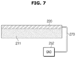
- FIG. 7 is an additional conceptual diagram illustrating a cross-section of an outer frame of the proximity sensor of FIG. 5 , according to embodiments of the present disclosure
- FIG. 8 is a conceptual diagram illustrating a cross-section of an inner frame of the proximity sensor of FIG. 5 , according to embodiments of the present disclosure
- FIG. 9 is an additional conceptual diagram illustrating a cross-section of an inner frame of the proximity sensor of FIG. 5 , according to embodiments of the present disclosure.
- FIG. 10 is an additional conceptual diagram illustrating a cross-section of an inner frame of the proximity sensor of FIG. 5 , according to embodiments of the present disclosure
- FIG. 12 is a conceptual diagram illustrating a cross-section of the proximity sensor shown in FIG. 5 ;
- FIG. 13 is an additional exploded view of a proximity sensor, according to embodiments of the present disclosure.
- FIG. 14 is a conceptual diagram illustrating a cross-section of the proximity sensor shown in FIG. 13 ;
- FIG. 15 is a conceptual diagram illustrating a sensing area of the proximity sensor when the outer frame is not connected to the ground (GND), according to embodiments of the present disclosure
- FIG. 16 is a conceptual diagram illustrating a sensing area of the proximity sensor when the outer frame is connected to the ground (GND), according to embodiments of the present disclosure.
- FIG. 17 is an additional exploded view of a proximity sensor, according to embodiments of the present disclosure.
- vehicle or “vehicular” or other similar term as used herein is inclusive of motor vehicles in general such as passenger automobiles including sports utility vehicles (SUV), buses, trucks, various commercial vehicles, watercraft including a variety of boats and ships, aircraft, and the like, and includes hybrid vehicles, electric vehicles, plug-in hybrid electric vehicles, hydrogen-powered vehicles and other alternative fuel vehicles (e.g., fuels derived from resources other than petroleum).
- a hybrid vehicle is a vehicle that has two or more sources of power, for example both gasoline-powered and electric-powered vehicles.
- controller may refer to a hardware device that includes a memory and a processor.
- the memory is configured to store program instructions, and the processor is specifically programmed to execute the program instructions to perform one or more processes which are described further below.
- the controller may control operation of units, modules, parts, or the like, as described herein.
- the below methods may be executed by an apparatus comprising the controller in conjunction with one or more other components, as would be appreciated by a person of ordinary skill in the art.
- controller of the present disclosure may be embodied as non-transitory computer readable media containing executable program instructions executed by a processor, controller or the like.
- Examples of the computer readable mediums include, but are not limited to, ROM, RAM, compact disc (CD)-ROMs, magnetic tapes, floppy disks, flash drives, smart cards and optical data storage devices.
- the computer readable recording medium can also be distributed throughout a computer network so that the program instructions are stored and executed in a distributed fashion, e.g., by a telematics server or a Controller Area Network (CAN).
- a telematics server or a Controller Area Network (CAN).
- CAN Controller Area Network
- FIG. 1 shows the exterior of a vehicle, according to embodiments of the present disclosure.
- the vehicle 100 may include a main body 1 that constitutes the exterior of the vehicle 100 , a front glass 30 that allows the driver inside the vehicle 100 to look ahead of the vehicle 100 , wheels 51 , 52 for moving the vehicle 100 , a driving system 60 for turning the wheels 51 , 52 , doors 71 that shield the inside of the vehicle 100 from outside, and side mirrors 81 , 82 that help the driver see areas behind and to the sides of the vehicle 100 .
- the front glass 30 also termed as a windshield glass, is placed on the top front of the main body 100 for the driver inside the vehicle 100 to obtain visual information about things in front of the vehicle 100 .
- the wheels 51 and 52 include front wheels 51 and rear wheels 52 , and the driving system 60 may provide turning forces to the front wheels 51 or rear wheels 52 to move the vehicle 100 forward or backward.
- the driving system 60 may employ a motor that produces the turning force from electrical power supplied from a storage battery (not shown) or a combustion engine (not shown) that burns a fuel to create the turning force.
- the doors 71 may be pivotally attached onto the left and right sides of the main body 1 , and opened for the driver and passenger to get on or get off the vehicle 100 and closed for shielding the inside of the vehicle 100 from outside.
- the doors 71 may have windows 72 installed thereon for the driver and passenger to look in or out through the windows 72 .
- the windows 72 may be installed to have only one viewable side and be opened and closed.
- the side mirrors 81 and 82 include a left side mirror 81 and a right side mirror 82 placed on the left and right sides of the main body 1 , respectively, for helping the driver obtain views behind and to the side of the vehicle 100 .
- FIG. 2 shows the interior of a vehicle, according to embodiments of the present disclosure.
- the vehicle 100 may include seats 110 reserved for driver and passengers to sit on, a gear box 120 , a center fascia 130 and a dashboard 150 having a steering wheel 140 .
- a gearshift 121 for shifting gears of the vehicle 100 may be installed in the gear box 120 .
- a dial adjuster 123 may be optionally installed as needed.
- an air conditioner 131 In the center fascia 130 , an air conditioner 131 , a clock 132 , an audio system 133 , and an Audio, Video, and Navigation (AVN) system 134 may be installed.
- APN Audio, Video, and Navigation
- the air conditioner 131 keeps the atmosphere inside the vehicle 100 pleasant by controlling temperature, humidity, air cleanness, and air flows inside the vehicle 100 .
- the air conditioner 131 may include at least one vent 131 a installed in the center fascia 130 for venting air. There may also be buttons or dials installed in the center fascia 130 to control e.g., the air conditioner 131 . The driver or the user may control the air conditioner 131 with the buttons arranged on the center fascia 130 .
- the clock 132 may be arranged around the buttons or dials for controlling the air conditioner 131 .
- the audio system 133 may include a control panel on which a number of buttons are mounted to perform functionality of the audio system 133 .
- the audio system 133 may provide a radio mode for radio listening and a media mode for reproducing audio files stored in various storage media.
- the AVN system 134 may be embedded in the center fascia 130 of the vehicle 100 .
- the AVN system 134 is a system for comprehensively performing audio, video and navigation functions of the vehicle 100 according to the user's manipulation.
- the AVN system 134 may include a display 135 for receiving user commands regarding the AVN system 134 and displaying a screen related to audio play, video play, or navigation.
- the center fascia 130 may also include a proximity sensor 200 provided to recognize an input means such as the user's hand or a touch pen approaching or making a contact.
- the proximity sensor 200 may recognize whether the user is approaching and touching thereto based on a change in capacity from the approach and touch of the user.
- FIG. 3 shows a center fascia of a vehicle with a proximity sensor installed therein, which is in a state before the user approaches thereto, according to embodiments of the present disclosure.
- FIG. 4 shows the proximity sensor shown in FIG. 3 in a state that the user approaches thereto.
- the proximity sensor 200 may be connected to a controller (not shown).
- the controller may control the air conditioner 131 , the audio system 133 , and the AVN system 134 .
- the proximity sensor 200 may recognize whether a user approaches thereto and send the related signal to the controller.
- the controller may control brightness of a light emitting unit (not shown) provided in the buttons, dials, and display of the air conditioner 131 , the audio system 133 , the AVN system 134 based on the received signal.
- the brightness of the light emitting unit provided in the buttons or dials on the center fascia remains low until a user approaches. This is to get rid of light pollution due to excessive indoor lighting during nighttime driving. During night time driving, too much indoor lighting unintended by the user may distract the user, which could lead to an accident. Accordingly, unintended power to the light emitting unit provided in the buttons on the center fascia may be blocked or the brightness level may be reduced to prevent disturbance of driving by the light.
- brightness of the light emitting unit provided in the button on the center fascia 130 may increase. This may enable the user to easily check the position or state of each button. In this way, if the user has an intention, this mechanism would not disturb driving from the light pollution even if the brightness of the light emitting unit increases but rather be helpful for driving because it makes it easy to locate the button. Furthermore, as the current state of a function may be indicated just by the approach of the user, high-tech image and classiness of the interior may be emphasized.
- the exterior of the proximity sensor 200 may be made of a metallic substance.
- the proximity sensor 200 in accordance with embodiments of the present disclosure has no problem with the use of non-transmissive metal because it includes a capacitive proximity sensor Integrated Circuit (IC).
- IC Integrated Circuit
- FIG. 5 is an exploded view of a proximity sensor, according to an embodiments of the present disclosure.
- the proximity sensor 200 may include a frame 210 arranged to be exposed to the outside of the center fascia 130 , a panel 240 coupled with the rear side of the frame 210 to support the frame 210 , a printed circuit board (PCB) 250 received inside the panel 240 , and a sensor IC 251 mounted on the PCB 250 .
- PCB printed circuit board
- the outer surface of the frame 210 may be provided with a metal layer 220 . Furthermore, there may be a sensor electrode 230 connected to the sensor IC 251 . The sensor electrode 230 may be connected to the PCB 250 and accordingly, to the sensor IC 251 .
- the frame 210 may be made of a non-conductive substance.
- the frame 210 may be made of plastics and manufactured by injection molding. There are no limitations on the shape of the frame 210 .
- a portion of the frame 210 may have a curved form and the frame 210 may include a bending portion.
- the frame 210 may include a bezel forming an outer boundary of the various buttons or display on the center fascia 130 . If the sensor IC may be able to detect approach of a user to the bezel, the sensor IC may recognize that the user is approaching to touch the buttons or touch parts arranged within the bezel. That is, when the proximity sensor is provided near the bezel, it may recognize the approach of the user to a button even if there is no extra proximity sensor provided for the button. However, as will be described later, the sensing area of the proximity sensor needs to be properly adjusted to prevent recognition of an unintended approach of a user.
- the frame 210 may include an outer frame 211 and an inner frame 212 .
- the outer frame may be formed of a first non-conductive substance.
- the inner frame may be formed of a second non-conductive substance.
- the first non-conductive substance and the second non-conductive substance may be the same material.
- the outer frame 211 may have the form of a closed loop. It is not, however, limited thereto, but may have the form of an open ring.
- the inner frame 212 may be disposed in an interior of the outer frame 211 .
- the inner frame 212 may divide the interior of the outer frame 211 , which has the form of a closed loop, into two or more.
- the inner frame has the form of a straight line in FIG. 5 , it is merely by way of example and the inner frame may have a curved form or may have changing thickness. In other words, there are no limitations on the form of the inner frame.
- the frame 210 may be exposed to the outside of the center fascia 130 . To meet the recent needs of users for metallic substances, the frame 210 may be made of a metallic substance.
- the entire frame 210 is manufactured of the metallic substance, it may weigh heavy and increase costs, causing an increase of manufacturing costs.
- the frame 210 is formed of plastics by e.g., injection molding as before, and after that, the outer surface of the frame 210 may be formed of a metallic substance by metal coating or Ion Plasma Evaporation (IPE).
- the outer surface of the frame 210 may be chromed.
- the metal layer 220 including the metallic substance may be formed on the outer surface of the frame 210 , which is exposed to the outside of the center fascia 130 .
- the outer surface of the frame 210 is formed of the metallic substance, classiness and beauty of the interior of the vehicle may be improved.
- FIG. 6 is a conceptual diagram illustrating a cross-section of an outer frame of the proximity sensor of FIG. 5 , according to embodiments of the present disclosure
- FIG. 7 is an additional conceptual diagram illustrating a cross-section of an outer frame of the proximity sensor of FIG. 5 , according to embodiments of the present disclosure.
- the metal layer 220 arranged on the outer surface of the outer frame 211 is called a first metal layer
- the metal layer 220 arranged on the inner frame 212 is called a second metal layer.
- the first metal layer 220 may be formed on the outer surface of the outer frame 211 .
- a primer layer 213 may be provided.
- the primer layer 213 may be arranged between the first metal layer 220 and the outer frame 211 .
- the metal layer 220 may be arranged right on the outer frame 211 without the primer layer.
- the first metal layer 220 may be connected to the ground GND.
- the ground may be variously provided.
- the ground GND may be formed on a ground layer 252 arranged on the PCB 250 (see FIG. 5 ).
- the ground GND may be formed at a chassis ground of the vehicle.
- the PCB 250 may be connected to the chassis ground of the vehicle. In the following description, an occasion when the ground layer 252 of the PCB 250 corresponds to the ground GND will be focused.
- the proximity sensor 200 may include a connector 270 connecting the first metal layer 220 and the ground GND 252 .
- the connector 270 may be variously provided as a configuration to electrically connect the first metal layer 220 and the ground GND 252 .
- the connector may be provided as a wire, a PCB, a flexible PCB, an injection molded product including a metal complex, and an injection molded product including an electrode by a Laser Directing Structure (LDS) method.
- the method for forming the connector may include any widely known method for electrically connecting two objects, such as metal vapor deposition or a method of extending a substance for plating to the ground GND from the first metal layer, a method of extending a substance including a conductive material to the ground GND from the first metal layer, or the like.
- the sensing field of the proximity sensor 200 may be confined to the inside of the first metal layer 220 .
- the proximity sensor 200 in an embodiment of the present disclosure may not recognize an unintended approach of a user. That is, it may get rid of noise. Furthermore, it may prevent damage to the sensor IC due to static electricity. This will be described in more detail later.
- FIGS. 8 to 11 are conceptual diagrams illustrating a cross-section of an inner frame of the proximity sensor of FIG. 5 , according to embodiments of the present disclosure.
- a sensor electrode 230 may be formed on a side of the inner frame 212 .
- the sensor electrode 230 may be formed using an LDS method.
- the LDS method refers to a method of forming a conductive structure in a region of a supporter member exposed to laser by forming the supporter member with a material including a non-conductive and chemically stable metal complex, exposing a metal seed by exposing a portion of the supporting member to laser, such as Ultra Violet (UV) laser or Excimer laser to break chemical bonding of the metal complex, and metalizing the supporting member.
- UV Ultra Violet
- the inner frame 212 may be made of a substance including a metal complex.
- An electrode recess (not shown) may be formed on the frame 210 by exposing the frame 210 to laser, and the electrode recess is metalized to form the sensor electrode 230 .
- the sensor electrode 230 may be arranged in some area of the outer surface of the inner frame 212 .
- the area of the outer surface of the inner frame 212 where the sensor electrode 230 is arranged may be very small as compared to the entire area of the outer surface of the inner frame 212 .
- the primer layer 213 may be formed on the other portion of the outer surface of the inner frame 212 than the portion where the sensor electrode 230 is arranged.
- the primer layer 213 is an element to stably couple the second metal layer 220 and the inner frame 212 , serving as a kind of adhesive.
- the primer layer 213 may be arranged on the inner frame 212 before the second metal layer 220 is formed.
- the primer layer 213 may be formed across a wider area than the area across which the sensor electrode 230 is arranged on the inner frame 212 .
- the primer layer 213 covers a portion of the sensor electrode 230 in FIG. 8 , it is not limited thereto.
- the primer layer 213 and the sensor electrode 230 may not overlap each other in some other embodiments.
- the primer layer 213 may be arranged in a partial area of the outer surface of the inner frame 212 .
- a metal plating area or metal vapor deposition area across which the second metal layer 220 is formed may be larger than the primer area across which the primer layer 213 is formed.
- the second metal layer 220 may cover the primer layer 213 and the sensor electrode 230 . Since the sensor electrode 230 and the second metal layer 220 have a structure of making a physical contact with each other, the sensor electrode 230 and the second metal layer 220 of a conductive metallic substance are electrically connected. Accordingly, the sensor IC 230 may detect the user approaching or contacting not only the sensor electrode 230 but also the second metal layer 220 electrically connected to the sensor electrode 230 . Accordingly, the second metal layer 220 may serve as a sensing part.
- the sensor electrode 230 formed on the inner frame 212 may be connected to the PCB 250 , and accordingly, to the sensor IC 251 mounted on the PCB 250 .
- the sensor electrode 230 may be connected to the PCB 250 in various ways.
- the proximity sensor 200 may include a flexible PCB that connects the sensor electrode 230 formed on the inner frame 212 and the PCB 250 .
- the sensor electrode 230 may be formed on the outer surface of the inner frame 212 , and the second metal layer 220 may be arranged right on the sensor electrode 230 without the primer layer.
- the second metal layer 220 and the sensor electrode 230 or the inner frame 212 may be relatively weak without the primer layer, productivity may be improved because the process of forming the primer layer can be omitted.
- the primer layer 213 may be arranged on the sensor electrode 230 , and the second metal layer 220 may be arranged on the primer layer 213 .
- the second metal layer 220 may be stably coupled with the inner frame 212 or the sensor electrode 230 . Since the primer layer 213 is very thin, the second metal layer 220 may serve as a sensing part even if the second metal layer 220 and the sensor electrode 230 are not in physical contact with each other. However, as compared with an occasion when the second metal layer 220 physically contacts the sensor electrode 230 , its sensitivity may be reduced.
- FIG. 9 is an additional conceptual diagram illustrating a cross-section of an inner frame of the proximity sensor of FIG. 5 , according to embodiments of the present disclosure.
- the second metal layer 220 may be arranged on the outer surface of the inner frame 212 , and the sensor electrode 230 may be arranged between the second metal layer 220 and the inner frame 212 .
- the second metal layer 220 may be arranged on one side of the inner frame 212 , and the sensor electrode 230 may be arranged on between the second metal layer 220 and the inner frame 212 .
- the sensor electrode 230 may be connected to the PCB 250 in various ways as in FIGS. 6 to 8 .
- the sensor electrode 230 may be formed on the inner frame 212 by the LDS method.
- the sensor electrode 230 and the second metal layer 220 may be separated by the thickness of the inner frame 212 . Since the thickness of the inner frame 212 is fixed, capacitance created between the second metal layer 220 and the sensor electrode 230 is constant. On the other hand, capacitance created between the user and the second metal layer 220 may change by the distance between the user and the second metal layer 220 . Accordingly, with the change in distance between the second metal layer 220 and the user, the capacitance of the sensor electrode 230 changes.
- the sensor IC 251 may detect the change in capacitance of the sensor electrode 230 . The sensor IC 251 may even detect a small change in capacitance of the sensor electrode 230 and recognize whether the user approaches or touches the second metal layer 220 based on the change in capacitance.
- FIG. 12 is a conceptual diagram illustrating a cross-section of the proximity sensor shown in FIG. 5 .
- the sensor electrode 230 may be formed on a side of a panel 240 .
- the sensor electrode 230 may be formed on a side of the panel 240 facing the inner frame 212 .
- the sensor electrode 230 may be formed using the LDS method.
- the panel 240 may be formed of a substance including a metal complex.
- the sensor electrode 230 may be arranged to be separated from the second metal layer 220 by a certain distance. As shown in FIG. 12 , the inner frame 212 and the sensor electrode 230 is separated by d 1 , and assuming that the thickness of the inner frame 212 is d 2 , the sensor electrode 230 and the second metal layer 220 may be separated by d 1 +d 2 . Since the thickness d 2 of the inner frame 212 and the distance d 1 between the sensor electrode 230 and the inner frame 212 are fixed, d 1 +d 2 is fixed. Accordingly, capacitance created between the second metal layer 220 and the sensor electrode 230 is constant.
- capacitance created between the user and the second metal layer 220 may change by the distance between the user and the second metal layer 220 . Accordingly, with the change in distance between the second metal layer 220 and the user, the capacitance of the sensor electrode 230 changes.
- the sensor IC 251 may detect the change in capacitance of the sensor electrode 230 .
- the sensor IC 251 may even detect a small change in capacitance of the sensor electrode 230 and recognize whether the user approaches or touches the second metal layer 220 based on the change in capacitance.
- an air layer may be formed in the empty space between the sensor electrode 230 and the inner frame 212 .
- the air layer formed between the sensor electrode 230 and the inner frame 212 even if a high voltage takes place instantaneously across the second metal layer 220 due to e.g., static electricity, the high voltage has little chance of being transferred to the sensor electrode 230 and the sensor IC 251 . Accordingly, the possibility for the sensor IC 251 to be damaged by the static electricity is very low. In other words, durability or stability of the sensor IC 251 may be improved.
- FIG. 13 is an additional exploded view of a proximity sensor, according to embodiments of the present disclosure
- FIG. 14 is a conceptual diagram illustrating a cross-section of the proximity sensor shown in FIG. 13 .
- the frame 210 may include an outer frame 211 and an inner frame 212 .
- the frame 210 was already described above, so the overlapping description thereof will not be repeated below.
- the proximity sensor 200 may include the frame 210 , the metal layer 220 formed on the outer surface of the frame 210 , the panel 240 coupled with the frame 210 , a sensor electrode base 260 having the sensor electrode 230 and coupled with the panel 240 , the PCB 250 received inside the panel 240 , and the sensor IC 251 mounted on the PCB 250 .
- the proximity sensor 200 may include the sensor electrode base 260 provided separately from the panel 240 and coupled with the panel 240 .
- the sensor electrode base 260 may include the sensor electrode 230 .
- the sensor electrode base 260 may be coupled with the panel 240 to connect the sensor electrode 230 to the PCB 250 .
- the sensor electrode 230 formed on the sensor electrode base 260 may be formed using the LDS method.
- the sensor electrode base 260 may be formed of a substance including a metal complex.
- the sensor electrode base 260 may be arranged to come into contact with the rear side of the inner frame 212 when coupled with the panel 240 .
- the sensor electrode 230 may come into contact with the rear side of the inner frame 212 .
- the second metal layer 220 may be formed on the front side of the inner frame 212 by metal plating or metal vapor deposition, and the second metal layer 220 may be formed after a primer layer (not shown) is formed on the front side of the inner frame 212 . As described above, it is preferable to have the primer layer for stable coupling of the second metal layer 220 and the inner frame 212 , but the primer layer may be omitted in some embodiments.
- the sensor electrode 230 and the second metal layer 220 may be separated by the thickness of the inner frame 212 . Since the thickness of the inner frame 212 is fixed, capacitance created between the second metal layer 220 and the sensor electrode 230 is constant. On the other hand, capacitance created between the user and the second metal layer 220 may change by the distance between the user and the second metal layer 220 . Accordingly, with the change in distance between the second metal layer 220 and the user, the capacitance of the sensor electrode 230 changes.
- the sensor IC 251 may detect the change in capacitance of the sensor electrode 230 . The sensor IC 251 may even detect a small change in capacitance of the sensor electrode 230 and recognize whether the user approaches or touches the second metal layer 220 based on the change in capacitance.
- an air layer may be formed between the sensor electrode 230 and the rear side of the inner frame 212 .
- the air layer is formed, a possibility for the sensor IC 251 to be damaged becomes low, so the durability of the sensor IC 251 may be improved.
- the manufacturing costs may be saved and the productivity may be improved.
- the sensor electrode base 260 may be easily coupled with the panel 240 by e.g., fitting.
- the entire panel 240 needs to be formed of a substance including a metal complex.
- the sensor electrode base 260 has smaller volume than the panel 240 , an increase in the manufacturing costs is less than using the panel 240 .
- the sensor electrode base 260 may be used in common with various forms of panels and accordingly, mass-produced, thereby saving the production cost.
- FIG. 15 is a conceptual diagram illustrating a sensing area of the proximity sensor when the outer frame is not connected to the ground (GND), according to embodiments of the present disclosure
- FIG. 16 is a conceptual diagram illustrating a sensing area of the proximity sensor when the outer frame is connected to the ground (GND), according to embodiments of the present disclosure.
- the second metal layer of the inner frame 212 may serve as a sensing part.
- the sensing area of the second metal layer is formed in all directions. Therefore, the sensing area may be formed in upward, downward, left, right, and rear directions in addition to the forward direction of the second metal layer. Some of the directions are intended by the designer, but the others may not be intended by the designer to recognize approach of the user, causing wrong recognition or noise.
- the outer frame 211 may serve as a bezel to form an outer boundary of the button portion. If the user approaches to touch the button portion, the user's finger may come within the boundary of the outer frame 211 that forms a closed loop. That is, the outer frame 211 may be a reference to set a range of the sensing area. For example, even if the user's finger approaches outside of the outer frame 211 , it is not the approach to touch the button portion, so the recognition of this by the proximity sensor 200 corresponds to recognition of noise. Accordingly, this noise needs to be eliminated.
- FIG. 16 shows the proximity sensor 200 with the sensing field confined to the interior the outer frame 211 to eliminate noise.
- the first metal layer of the outer frame 211 is connected to the ground GND.
- the connector 270 may be variously provided as described above. If there is the ground GND, an electric field vector that forms the sensing field converges to the ground GND, so the sensing field is confined to the interior of the outer frame 211 . In other words, the outer frame 211 connected to the ground GND may shield the sensing field within the outer frame 211 .
- FIG. 17 is an additional exploded view of a proximity sensor, according to embodiments of the present disclosure.
- the inner frame 212 may include a first inner frame 212 a , a second inner frame 212 b , and a third inner frame 212 c , which are separated from one another.
- the first metal layer 220 may be formed on the outer surface of each of the first, second, and third inner frames 212 a , 212 b , 212 c.
- the first metal layer formed on the first inner frame 212 a may be electrically connected to the sensor electrode 230 , and accordingly, to the sensor IC 251 . This enables the first metal layer formed on the first inner frame 212 a to serve as a sensing part.
- the first metal layers formed on the second and third inner frames 212 b and 212 c may not be electrically connected to the sensor electrode 230 , thereby not serving as sensing parts. In other words, even if the first metal layers formed on the second and third inner frames 212 b and 212 c are touched, the proximity sensor 200 may not recognize them.
- the user's body parts such as knees may come into contact with the proximity sensor according to the position of the proximity sensor and the user's habit.
- the right knee of the driver may contact the left end of the inner frame 212 and the passenger's left knee may contact the right end of the inner frame 212 .
- Such contacts are not intended to touch or push a button but correspond to noise, so the proximity sensor should not recognize them.
- the proximity sensor 200 may not recognize it. That is, it may get rid of noise.
- the first inner frame 212 a may happen to contact the second inner frame 212 b or the third inner frame 212 c .
- the first metal layers come into contact with each other, and thus the second inner frame 212 b and the third inner frame 212 may serve as sensing parts.
- the noise such as recognition of knee touch may not be eliminated.
- the ribs 241 may be integrated into the panel 240 without being limited thereto.
- a proximity sensor as described herein may have the metallic exterior to give improved aesthetic feeling.
- a proximity sensor may be provided having an easily manufactured design and simple structure.
- a proximity sensor may be provided having efficient space utilization because it requires no extra installation space.
- a proximity sensor may be provided having improved substance selection and degree of freedom for design.
- a proximity sensor may be provided to have reduced noise-making frequency by revising its sensing area.
Landscapes
- Engineering & Computer Science (AREA)
- General Engineering & Computer Science (AREA)
- Theoretical Computer Science (AREA)
- Physics & Mathematics (AREA)
- General Physics & Mathematics (AREA)
- Human Computer Interaction (AREA)
- Life Sciences & Earth Sciences (AREA)
- Remote Sensing (AREA)
- Electromagnetism (AREA)
- Environmental & Geological Engineering (AREA)
- Geology (AREA)
- General Life Sciences & Earth Sciences (AREA)
- Geophysics (AREA)
- Transportation (AREA)
- Mechanical Engineering (AREA)
- Switches That Are Operated By Magnetic Or Electric Fields (AREA)
Abstract
Description
Claims (9)
Applications Claiming Priority (2)
| Application Number | Priority Date | Filing Date | Title |
|---|---|---|---|
| KR10-2017-0154416 | 2017-11-20 | ||
| KR1020170154416A KR102464610B1 (en) | 2017-11-20 | 2017-11-20 | Proximity sensor |
Publications (2)
| Publication Number | Publication Date |
|---|---|
| US20190152391A1 US20190152391A1 (en) | 2019-05-23 |
| US11155206B2 true US11155206B2 (en) | 2021-10-26 |
Family
ID=66336653
Family Applications (1)
| Application Number | Title | Priority Date | Filing Date |
|---|---|---|---|
| US16/175,070 Active 2039-07-24 US11155206B2 (en) | 2017-11-20 | 2018-10-30 | Proximity sensor |
Country Status (4)
| Country | Link |
|---|---|
| US (1) | US11155206B2 (en) |
| KR (1) | KR102464610B1 (en) |
| CN (1) | CN109814154B (en) |
| DE (1) | DE102018219111A1 (en) |
Families Citing this family (1)
| Publication number | Priority date | Publication date | Assignee | Title |
|---|---|---|---|---|
| KR102499566B1 (en) | 2021-08-11 | 2023-02-14 | 현대트랜시스 주식회사 | Capacitive touch type power seat switch using receptacle |
Citations (5)
| Publication number | Priority date | Publication date | Assignee | Title |
|---|---|---|---|---|
| US20110057669A1 (en) * | 2009-09-08 | 2011-03-10 | Amlogic Co., Ltd. | Capacitive Sensor |
| US20130001058A1 (en) * | 2011-07-01 | 2013-01-03 | Phantom-Products LLC | Vehicle touch button |
| US20130170013A1 (en) * | 2002-09-30 | 2013-07-04 | Gentex Corporation | Automotive rearview mirror with capacitive switches |
| US20140177176A1 (en) * | 2012-12-21 | 2014-06-26 | Canon Kabushiki Kaisha | Panel unit that reduces influence of static electricity, and electronic apparatus |
| US20170017335A1 (en) * | 2014-03-28 | 2017-01-19 | Kaneka Corporation | Touch panel, display device, and touch panel manufacturing method |
Family Cites Families (5)
| Publication number | Priority date | Publication date | Assignee | Title |
|---|---|---|---|---|
| US9335868B2 (en) * | 2008-07-31 | 2016-05-10 | Apple Inc. | Capacitive sensor behind black mask |
| DE102012105117A1 (en) * | 2012-06-13 | 2013-12-19 | Huf Hülsbeck & Fürst Gmbh & Co. Kg | Approach detecting device |
| DE102012109031A1 (en) * | 2012-09-25 | 2014-03-27 | Huf Hülsbeck & Fürst Gmbh & Co. Kg | Electronic sensor unit for detecting the contactless actuation of a door or flap on a motor vehicle |
| US9559425B2 (en) * | 2014-03-20 | 2017-01-31 | Apple Inc. | Electronic device with slot antenna and proximity sensor |
| EP2988479B1 (en) * | 2014-08-19 | 2019-01-30 | Semtech Corporation | Capacitive proximity sensor and mobile device |
-
2017
- 2017-11-20 KR KR1020170154416A patent/KR102464610B1/en active Active
-
2018
- 2018-10-30 US US16/175,070 patent/US11155206B2/en active Active
- 2018-11-09 DE DE102018219111.5A patent/DE102018219111A1/en active Pending
- 2018-11-20 CN CN201811388271.3A patent/CN109814154B/en active Active
Patent Citations (5)
| Publication number | Priority date | Publication date | Assignee | Title |
|---|---|---|---|---|
| US20130170013A1 (en) * | 2002-09-30 | 2013-07-04 | Gentex Corporation | Automotive rearview mirror with capacitive switches |
| US20110057669A1 (en) * | 2009-09-08 | 2011-03-10 | Amlogic Co., Ltd. | Capacitive Sensor |
| US20130001058A1 (en) * | 2011-07-01 | 2013-01-03 | Phantom-Products LLC | Vehicle touch button |
| US20140177176A1 (en) * | 2012-12-21 | 2014-06-26 | Canon Kabushiki Kaisha | Panel unit that reduces influence of static electricity, and electronic apparatus |
| US20170017335A1 (en) * | 2014-03-28 | 2017-01-19 | Kaneka Corporation | Touch panel, display device, and touch panel manufacturing method |
Also Published As
| Publication number | Publication date |
|---|---|
| CN109814154A (en) | 2019-05-28 |
| US20190152391A1 (en) | 2019-05-23 |
| KR20190057474A (en) | 2019-05-29 |
| KR102464610B1 (en) | 2022-11-08 |
| DE102018219111A1 (en) | 2019-05-23 |
| CN109814154B (en) | 2023-05-26 |
Similar Documents
| Publication | Publication Date | Title |
|---|---|---|
| CN107150643B (en) | Vehicle and its control method | |
| US20110134054A1 (en) | Input device of touch panel type for vehicle | |
| EP3072710B1 (en) | Vehicle, mobile terminal and method for controlling the same | |
| US10180729B2 (en) | Human machine interface apparatus for vehicle and methods of controlling the same | |
| US10983691B2 (en) | Terminal, vehicle having the terminal, and method for controlling the vehicle | |
| US20090174533A1 (en) | Instrumentation Assembly For A Vehicle | |
| US20090174682A1 (en) | Instrumentation Module For A Vehicle | |
| CN115431761B (en) | Vehicle-mounted display device, vehicle steering wheel assembly and vehicle | |
| WO2009089092A1 (en) | Touch sensitive switches integrated with a vehicle interior part | |
| CN104010864B (en) | Configurable control panel | |
| US10476501B2 (en) | Capacitive sensor and switch assembly with decorative conductive component | |
| US9073433B2 (en) | Vehicle control system | |
| US20180302088A1 (en) | Proximity switch having sensor with decorative metal | |
| US10523200B2 (en) | Proximity sensor | |
| US11155206B2 (en) | Proximity sensor | |
| US20170282953A1 (en) | Vehicle accessory control circuit | |
| KR102441515B1 (en) | Vehicle input device | |
| CN109747418B (en) | Control panel for vehicle | |
| KR101879870B1 (en) | Input apparatus, vehicle and method of controlling thereof | |
| KR20180066009A (en) | Input apparatus, vehicle comprising the same and control method for the input apparatus | |
| KR20180004932A (en) | Input apparatus, vehicle comprising the same and control method for the input apparatus | |
| KR20190069651A (en) | Display Apparatus And Having The Same Vehicle | |
| KR20190083927A (en) | Touch control device and vehicle comprising the same | |
| KR20180046038A (en) | Wireless charge apparatus, vehicle and method of controlling thereof |
Legal Events
| Date | Code | Title | Description |
|---|---|---|---|
| AS | Assignment |
Owner name: KIA MOTORS CORPORATION, KOREA, REPUBLIC OF Free format text: ASSIGNMENT OF ASSIGNORS INTEREST;ASSIGNORS:KWON, GIDEOK;OH, SEOK JUN;KIM, MOO YONG;AND OTHERS;REEL/FRAME:047358/0961 Effective date: 20180514 Owner name: HYUNDAI MOTOR COMPANY, KOREA, REPUBLIC OF Free format text: ASSIGNMENT OF ASSIGNORS INTEREST;ASSIGNORS:KWON, GIDEOK;OH, SEOK JUN;KIM, MOO YONG;AND OTHERS;REEL/FRAME:047358/0961 Effective date: 20180514 |
|
| FEPP | Fee payment procedure |
Free format text: ENTITY STATUS SET TO UNDISCOUNTED (ORIGINAL EVENT CODE: BIG.); ENTITY STATUS OF PATENT OWNER: LARGE ENTITY |
|
| STPP | Information on status: patent application and granting procedure in general |
Free format text: DOCKETED NEW CASE - READY FOR EXAMINATION |
|
| STPP | Information on status: patent application and granting procedure in general |
Free format text: RESPONSE TO NON-FINAL OFFICE ACTION ENTERED AND FORWARDED TO EXAMINER |
|
| STPP | Information on status: patent application and granting procedure in general |
Free format text: NON FINAL ACTION MAILED |
|
| STPP | Information on status: patent application and granting procedure in general |
Free format text: RESPONSE TO NON-FINAL OFFICE ACTION ENTERED AND FORWARDED TO EXAMINER |
|
| STPP | Information on status: patent application and granting procedure in general |
Free format text: NOTICE OF ALLOWANCE MAILED -- APPLICATION RECEIVED IN OFFICE OF PUBLICATIONS |
|
| STPP | Information on status: patent application and granting procedure in general |
Free format text: PUBLICATIONS -- ISSUE FEE PAYMENT VERIFIED |
|
| STCF | Information on status: patent grant |
Free format text: PATENTED CASE |
|
| MAFP | Maintenance fee payment |
Free format text: PAYMENT OF MAINTENANCE FEE, 4TH YEAR, LARGE ENTITY (ORIGINAL EVENT CODE: M1551); ENTITY STATUS OF PATENT OWNER: LARGE ENTITY Year of fee payment: 4 |