US11150505B2 - Display panel and display device - Google Patents
Display panel and display device Download PDFInfo
- Publication number
- US11150505B2 US11150505B2 US16/433,918 US201916433918A US11150505B2 US 11150505 B2 US11150505 B2 US 11150505B2 US 201916433918 A US201916433918 A US 201916433918A US 11150505 B2 US11150505 B2 US 11150505B2
- Authority
- US
- United States
- Prior art keywords
- substrate
- display panel
- light collecting
- collecting structure
- base substrate
- Prior art date
- Legal status (The legal status is an assumption and is not a legal conclusion. Google has not performed a legal analysis and makes no representation as to the accuracy of the status listed.)
- Active, expires
Links
Images


Classifications
-
- H—ELECTRICITY
- H10—SEMICONDUCTOR DEVICES; ELECTRIC SOLID-STATE DEVICES NOT OTHERWISE PROVIDED FOR
- H10F—INORGANIC SEMICONDUCTOR DEVICES SENSITIVE TO INFRARED RADIATION, LIGHT, ELECTROMAGNETIC RADIATION OF SHORTER WAVELENGTH OR CORPUSCULAR RADIATION
- H10F30/00—Individual radiation-sensitive semiconductor devices in which radiation controls the flow of current through the devices, e.g. photodetectors
- H10F30/20—Individual radiation-sensitive semiconductor devices in which radiation controls the flow of current through the devices, e.g. photodetectors the devices having potential barriers, e.g. phototransistors
- H10F30/21—Individual radiation-sensitive semiconductor devices in which radiation controls the flow of current through the devices, e.g. photodetectors the devices having potential barriers, e.g. phototransistors the devices being sensitive to infrared, visible or ultraviolet radiation
- H10F30/22—Individual radiation-sensitive semiconductor devices in which radiation controls the flow of current through the devices, e.g. photodetectors the devices having potential barriers, e.g. phototransistors the devices being sensitive to infrared, visible or ultraviolet radiation the devices having only one potential barrier, e.g. photodiodes
- H10F30/221—Individual radiation-sensitive semiconductor devices in which radiation controls the flow of current through the devices, e.g. photodetectors the devices having potential barriers, e.g. phototransistors the devices being sensitive to infrared, visible or ultraviolet radiation the devices having only one potential barrier, e.g. photodiodes the potential barrier being a PN homojunction
-
- G—PHYSICS
- G02—OPTICS
- G02F—OPTICAL DEVICES OR ARRANGEMENTS FOR THE CONTROL OF LIGHT BY MODIFICATION OF THE OPTICAL PROPERTIES OF THE MEDIA OF THE ELEMENTS INVOLVED THEREIN; NON-LINEAR OPTICS; FREQUENCY-CHANGING OF LIGHT; OPTICAL LOGIC ELEMENTS; OPTICAL ANALOGUE/DIGITAL CONVERTERS
- G02F1/00—Devices or arrangements for the control of the intensity, colour, phase, polarisation or direction of light arriving from an independent light source, e.g. switching, gating or modulating; Non-linear optics
- G02F1/01—Devices or arrangements for the control of the intensity, colour, phase, polarisation or direction of light arriving from an independent light source, e.g. switching, gating or modulating; Non-linear optics for the control of the intensity, phase, polarisation or colour
- G02F1/13—Devices or arrangements for the control of the intensity, colour, phase, polarisation or direction of light arriving from an independent light source, e.g. switching, gating or modulating; Non-linear optics for the control of the intensity, phase, polarisation or colour based on liquid crystals, e.g. single liquid crystal display cells
- G02F1/133—Constructional arrangements; Operation of liquid crystal cells; Circuit arrangements
- G02F1/1333—Constructional arrangements; Manufacturing methods
- G02F1/13338—Input devices, e.g. touch panels
-
- G—PHYSICS
- G02—OPTICS
- G02F—OPTICAL DEVICES OR ARRANGEMENTS FOR THE CONTROL OF LIGHT BY MODIFICATION OF THE OPTICAL PROPERTIES OF THE MEDIA OF THE ELEMENTS INVOLVED THEREIN; NON-LINEAR OPTICS; FREQUENCY-CHANGING OF LIGHT; OPTICAL LOGIC ELEMENTS; OPTICAL ANALOGUE/DIGITAL CONVERTERS
- G02F1/00—Devices or arrangements for the control of the intensity, colour, phase, polarisation or direction of light arriving from an independent light source, e.g. switching, gating or modulating; Non-linear optics
- G02F1/01—Devices or arrangements for the control of the intensity, colour, phase, polarisation or direction of light arriving from an independent light source, e.g. switching, gating or modulating; Non-linear optics for the control of the intensity, phase, polarisation or colour
- G02F1/13—Devices or arrangements for the control of the intensity, colour, phase, polarisation or direction of light arriving from an independent light source, e.g. switching, gating or modulating; Non-linear optics for the control of the intensity, phase, polarisation or colour based on liquid crystals, e.g. single liquid crystal display cells
- G02F1/133—Constructional arrangements; Operation of liquid crystal cells; Circuit arrangements
- G02F1/1333—Constructional arrangements; Manufacturing methods
- G02F1/1335—Structural association of cells with optical devices, e.g. polarisers or reflectors
- G02F1/133509—Filters, e.g. light shielding masks
- G02F1/133512—Light shielding layers, e.g. black matrix
-
- G—PHYSICS
- G02—OPTICS
- G02F—OPTICAL DEVICES OR ARRANGEMENTS FOR THE CONTROL OF LIGHT BY MODIFICATION OF THE OPTICAL PROPERTIES OF THE MEDIA OF THE ELEMENTS INVOLVED THEREIN; NON-LINEAR OPTICS; FREQUENCY-CHANGING OF LIGHT; OPTICAL LOGIC ELEMENTS; OPTICAL ANALOGUE/DIGITAL CONVERTERS
- G02F1/00—Devices or arrangements for the control of the intensity, colour, phase, polarisation or direction of light arriving from an independent light source, e.g. switching, gating or modulating; Non-linear optics
- G02F1/01—Devices or arrangements for the control of the intensity, colour, phase, polarisation or direction of light arriving from an independent light source, e.g. switching, gating or modulating; Non-linear optics for the control of the intensity, phase, polarisation or colour
- G02F1/13—Devices or arrangements for the control of the intensity, colour, phase, polarisation or direction of light arriving from an independent light source, e.g. switching, gating or modulating; Non-linear optics for the control of the intensity, phase, polarisation or colour based on liquid crystals, e.g. single liquid crystal display cells
- G02F1/133—Constructional arrangements; Operation of liquid crystal cells; Circuit arrangements
- G02F1/1333—Constructional arrangements; Manufacturing methods
- G02F1/1335—Structural association of cells with optical devices, e.g. polarisers or reflectors
- G02F1/133509—Filters, e.g. light shielding masks
- G02F1/133514—Colour filters
-
- G—PHYSICS
- G02—OPTICS
- G02F—OPTICAL DEVICES OR ARRANGEMENTS FOR THE CONTROL OF LIGHT BY MODIFICATION OF THE OPTICAL PROPERTIES OF THE MEDIA OF THE ELEMENTS INVOLVED THEREIN; NON-LINEAR OPTICS; FREQUENCY-CHANGING OF LIGHT; OPTICAL LOGIC ELEMENTS; OPTICAL ANALOGUE/DIGITAL CONVERTERS
- G02F1/00—Devices or arrangements for the control of the intensity, colour, phase, polarisation or direction of light arriving from an independent light source, e.g. switching, gating or modulating; Non-linear optics
- G02F1/01—Devices or arrangements for the control of the intensity, colour, phase, polarisation or direction of light arriving from an independent light source, e.g. switching, gating or modulating; Non-linear optics for the control of the intensity, phase, polarisation or colour
- G02F1/13—Devices or arrangements for the control of the intensity, colour, phase, polarisation or direction of light arriving from an independent light source, e.g. switching, gating or modulating; Non-linear optics for the control of the intensity, phase, polarisation or colour based on liquid crystals, e.g. single liquid crystal display cells
- G02F1/133—Constructional arrangements; Operation of liquid crystal cells; Circuit arrangements
- G02F1/1333—Constructional arrangements; Manufacturing methods
- G02F1/1335—Structural association of cells with optical devices, e.g. polarisers or reflectors
- G02F1/133526—Lenses, e.g. microlenses or Fresnel lenses
-
- G—PHYSICS
- G02—OPTICS
- G02F—OPTICAL DEVICES OR ARRANGEMENTS FOR THE CONTROL OF LIGHT BY MODIFICATION OF THE OPTICAL PROPERTIES OF THE MEDIA OF THE ELEMENTS INVOLVED THEREIN; NON-LINEAR OPTICS; FREQUENCY-CHANGING OF LIGHT; OPTICAL LOGIC ELEMENTS; OPTICAL ANALOGUE/DIGITAL CONVERTERS
- G02F1/00—Devices or arrangements for the control of the intensity, colour, phase, polarisation or direction of light arriving from an independent light source, e.g. switching, gating or modulating; Non-linear optics
- G02F1/01—Devices or arrangements for the control of the intensity, colour, phase, polarisation or direction of light arriving from an independent light source, e.g. switching, gating or modulating; Non-linear optics for the control of the intensity, phase, polarisation or colour
- G02F1/13—Devices or arrangements for the control of the intensity, colour, phase, polarisation or direction of light arriving from an independent light source, e.g. switching, gating or modulating; Non-linear optics for the control of the intensity, phase, polarisation or colour based on liquid crystals, e.g. single liquid crystal display cells
- G02F1/133—Constructional arrangements; Operation of liquid crystal cells; Circuit arrangements
- G02F1/1333—Constructional arrangements; Manufacturing methods
- G02F1/1335—Structural association of cells with optical devices, e.g. polarisers or reflectors
- G02F1/13356—Structural association of cells with optical devices, e.g. polarisers or reflectors characterised by the placement of the optical elements
- G02F1/133562—Structural association of cells with optical devices, e.g. polarisers or reflectors characterised by the placement of the optical elements on the viewer side
-
- G—PHYSICS
- G02—OPTICS
- G02F—OPTICAL DEVICES OR ARRANGEMENTS FOR THE CONTROL OF LIGHT BY MODIFICATION OF THE OPTICAL PROPERTIES OF THE MEDIA OF THE ELEMENTS INVOLVED THEREIN; NON-LINEAR OPTICS; FREQUENCY-CHANGING OF LIGHT; OPTICAL LOGIC ELEMENTS; OPTICAL ANALOGUE/DIGITAL CONVERTERS
- G02F1/00—Devices or arrangements for the control of the intensity, colour, phase, polarisation or direction of light arriving from an independent light source, e.g. switching, gating or modulating; Non-linear optics
- G02F1/01—Devices or arrangements for the control of the intensity, colour, phase, polarisation or direction of light arriving from an independent light source, e.g. switching, gating or modulating; Non-linear optics for the control of the intensity, phase, polarisation or colour
- G02F1/13—Devices or arrangements for the control of the intensity, colour, phase, polarisation or direction of light arriving from an independent light source, e.g. switching, gating or modulating; Non-linear optics for the control of the intensity, phase, polarisation or colour based on liquid crystals, e.g. single liquid crystal display cells
- G02F1/133—Constructional arrangements; Operation of liquid crystal cells; Circuit arrangements
- G02F1/1333—Constructional arrangements; Manufacturing methods
- G02F1/1335—Structural association of cells with optical devices, e.g. polarisers or reflectors
- G02F1/13356—Structural association of cells with optical devices, e.g. polarisers or reflectors characterised by the placement of the optical elements
- G02F1/133565—Structural association of cells with optical devices, e.g. polarisers or reflectors characterised by the placement of the optical elements inside the LC elements, i.e. between the cell substrates
-
- G—PHYSICS
- G02—OPTICS
- G02F—OPTICAL DEVICES OR ARRANGEMENTS FOR THE CONTROL OF LIGHT BY MODIFICATION OF THE OPTICAL PROPERTIES OF THE MEDIA OF THE ELEMENTS INVOLVED THEREIN; NON-LINEAR OPTICS; FREQUENCY-CHANGING OF LIGHT; OPTICAL LOGIC ELEMENTS; OPTICAL ANALOGUE/DIGITAL CONVERTERS
- G02F1/00—Devices or arrangements for the control of the intensity, colour, phase, polarisation or direction of light arriving from an independent light source, e.g. switching, gating or modulating; Non-linear optics
- G02F1/01—Devices or arrangements for the control of the intensity, colour, phase, polarisation or direction of light arriving from an independent light source, e.g. switching, gating or modulating; Non-linear optics for the control of the intensity, phase, polarisation or colour
- G02F1/13—Devices or arrangements for the control of the intensity, colour, phase, polarisation or direction of light arriving from an independent light source, e.g. switching, gating or modulating; Non-linear optics for the control of the intensity, phase, polarisation or colour based on liquid crystals, e.g. single liquid crystal display cells
- G02F1/133—Constructional arrangements; Operation of liquid crystal cells; Circuit arrangements
- G02F1/136—Liquid crystal cells structurally associated with a semi-conducting layer or substrate, e.g. cells forming part of an integrated circuit
- G02F1/1362—Active matrix addressed cells
- G02F1/1368—Active matrix addressed cells in which the switching element is a three-electrode device
-
- G—PHYSICS
- G06—COMPUTING OR CALCULATING; COUNTING
- G06F—ELECTRIC DIGITAL DATA PROCESSING
- G06F3/00—Input arrangements for transferring data to be processed into a form capable of being handled by the computer; Output arrangements for transferring data from processing unit to output unit, e.g. interface arrangements
- G06F3/01—Input arrangements or combined input and output arrangements for interaction between user and computer
- G06F3/03—Arrangements for converting the position or the displacement of a member into a coded form
- G06F3/041—Digitisers, e.g. for touch screens or touch pads, characterised by the transducing means
- G06F3/0412—Digitisers structurally integrated in a display
-
- G—PHYSICS
- G06—COMPUTING OR CALCULATING; COUNTING
- G06V—IMAGE OR VIDEO RECOGNITION OR UNDERSTANDING
- G06V10/00—Arrangements for image or video recognition or understanding
- G06V10/10—Image acquisition
- G06V10/12—Details of acquisition arrangements; Constructional details thereof
- G06V10/14—Optical characteristics of the device performing the acquisition or on the illumination arrangements
- G06V10/143—Sensing or illuminating at different wavelengths
-
- G—PHYSICS
- G06—COMPUTING OR CALCULATING; COUNTING
- G06V—IMAGE OR VIDEO RECOGNITION OR UNDERSTANDING
- G06V40/00—Recognition of biometric, human-related or animal-related patterns in image or video data
- G06V40/10—Human or animal bodies, e.g. vehicle occupants or pedestrians; Body parts, e.g. hands
- G06V40/12—Fingerprints or palmprints
- G06V40/13—Sensors therefor
- G06V40/1318—Sensors therefor using electro-optical elements or layers, e.g. electroluminescent sensing
-
- G—PHYSICS
- G06—COMPUTING OR CALCULATING; COUNTING
- G06V—IMAGE OR VIDEO RECOGNITION OR UNDERSTANDING
- G06V40/00—Recognition of biometric, human-related or animal-related patterns in image or video data
- G06V40/10—Human or animal bodies, e.g. vehicle occupants or pedestrians; Body parts, e.g. hands
- G06V40/12—Fingerprints or palmprints
- G06V40/1365—Matching; Classification
-
- H01L27/1214—
-
- H01L31/103—
-
- H01L31/12—
-
- H—ELECTRICITY
- H10—SEMICONDUCTOR DEVICES; ELECTRIC SOLID-STATE DEVICES NOT OTHERWISE PROVIDED FOR
- H10D—INORGANIC ELECTRIC SEMICONDUCTOR DEVICES
- H10D86/00—Integrated devices formed in or on insulating or conducting substrates, e.g. formed in silicon-on-insulator [SOI] substrates or on stainless steel or glass substrates
- H10D86/40—Integrated devices formed in or on insulating or conducting substrates, e.g. formed in silicon-on-insulator [SOI] substrates or on stainless steel or glass substrates characterised by multiple TFTs
- H10D86/60—Integrated devices formed in or on insulating or conducting substrates, e.g. formed in silicon-on-insulator [SOI] substrates or on stainless steel or glass substrates characterised by multiple TFTs wherein the TFTs are in active matrices
-
- H—ELECTRICITY
- H10—SEMICONDUCTOR DEVICES; ELECTRIC SOLID-STATE DEVICES NOT OTHERWISE PROVIDED FOR
- H10F—INORGANIC SEMICONDUCTOR DEVICES SENSITIVE TO INFRARED RADIATION, LIGHT, ELECTROMAGNETIC RADIATION OF SHORTER WAVELENGTH OR CORPUSCULAR RADIATION
- H10F55/00—Radiation-sensitive semiconductor devices covered by groups H10F10/00, H10F19/00 or H10F30/00 being structurally associated with electric light sources and electrically or optically coupled thereto
-
- H—ELECTRICITY
- H10—SEMICONDUCTOR DEVICES; ELECTRIC SOLID-STATE DEVICES NOT OTHERWISE PROVIDED FOR
- H10F—INORGANIC SEMICONDUCTOR DEVICES SENSITIVE TO INFRARED RADIATION, LIGHT, ELECTROMAGNETIC RADIATION OF SHORTER WAVELENGTH OR CORPUSCULAR RADIATION
- H10F77/00—Constructional details of devices covered by this subclass
- H10F77/40—Optical elements or arrangements
- H10F77/407—Optical elements or arrangements indirectly associated with the devices
-
- G—PHYSICS
- G02—OPTICS
- G02F—OPTICAL DEVICES OR ARRANGEMENTS FOR THE CONTROL OF LIGHT BY MODIFICATION OF THE OPTICAL PROPERTIES OF THE MEDIA OF THE ELEMENTS INVOLVED THEREIN; NON-LINEAR OPTICS; FREQUENCY-CHANGING OF LIGHT; OPTICAL LOGIC ELEMENTS; OPTICAL ANALOGUE/DIGITAL CONVERTERS
- G02F1/00—Devices or arrangements for the control of the intensity, colour, phase, polarisation or direction of light arriving from an independent light source, e.g. switching, gating or modulating; Non-linear optics
- G02F1/01—Devices or arrangements for the control of the intensity, colour, phase, polarisation or direction of light arriving from an independent light source, e.g. switching, gating or modulating; Non-linear optics for the control of the intensity, phase, polarisation or colour
- G02F1/13—Devices or arrangements for the control of the intensity, colour, phase, polarisation or direction of light arriving from an independent light source, e.g. switching, gating or modulating; Non-linear optics for the control of the intensity, phase, polarisation or colour based on liquid crystals, e.g. single liquid crystal display cells
- G02F1/133—Constructional arrangements; Operation of liquid crystal cells; Circuit arrangements
- G02F1/1333—Constructional arrangements; Manufacturing methods
- G02F1/133357—Planarisation layers
Definitions
- the present disclosure generally relates to the field of display technologies and, in particular, relates to a display panel and a display device.
- a display device integrates an optical sensor in a display panel and uses the optical sensor to implement the fingerprint recognition function.
- the optical sensor is difficult to receive sufficient light to recognize the fingerprint, resulting in lower accuracy of fingerprint recognition and lowering the user experience.
- the present disclosure provides a display panel including: a first substrate, a second substrate, and a liquid crystal layer between the first substrate and the second substrate.
- the first substrate includes a first base substrate and an optical sensor disposed on the first base substrate.
- the second substrate includes a second base substrate, a black matrix disposed on the second base substrate, and a light collecting structure disposed on a side of the black matrix adjacent to the first substrate.
- the optical sensor and the light collecting structure overlap each other in a direction perpendicular to the display panel.
- the light collecting structure includes at least one transparent protrusion protruded along a direction perpendicular to a surface of the first or second substrate and from the second substrate to the first substrate.
- a refractive index of the light collecting structure is larger than a refractive index of the liquid crystal layer.
- the present disclosure provides a display device including the display panel.
- the display panel includes a first substrate, a second substrate, and a liquid crystal layer between the first substrate and the second substrate.
- the first substrate includes a first base substrate and an optical sensor disposed on the first base substrate.
- the second substrate includes a second base substrate, a black matrix disposed on the second base substrate, and a light collecting structure disposed on a side of the black matrix adjacent to the first substrate.
- the optical sensor and the light collecting structure overlap each other in a direction perpendicular to the display panel.
- the light collecting structure includes at least one transparent protrusion protruded along a direction perpendicular to a surface of the first or second substrate and from the second substrate to the first substrate.
- a refractive index of the light collecting structure is larger than a refractive index of the liquid crystal layer.
- FIG. 1 is a schematic cross-sectional structural view of a display panel according to the prior art
- FIG. 2 is a schematic cross-sectional structural view of a display panel according to an exemplary embodiment of the present disclosure
- FIG. 3 is an optical path diagram of the display panel shown in FIG. 2 during fingerprint recognition
- FIG. 5 is a schematic cross-sectional structural view of another display panel according to an exemplary embodiment of the present disclosure.
- FIG. 6 is a schematic cross-sectional structural view of another display panel according to an exemplary embodiment of the present disclosure.
- FIG. 7 is a schematic cross-sectional structural view of another display panel according to an exemplary embodiment of the present disclosure.
- FIG. 8 is an optical path diagram of a light collecting structure in another display panel according to an exemplary embodiment of the present disclosure.
- FIG. 9 is an optical path diagram of a light collecting structure in another display panel according to an exemplary embodiment of the present disclosure.
- FIG. 10 is an optical path diagram of a light collecting structure in another display panel according to an exemplary embodiment of the present disclosure.
- FIG. 11 is a schematic cross-sectional structural view of another display panel according to an exemplary embodiment of the present disclosure.
- FIG. 14 is a schematic cross-sectional structural view of another display panel according to an exemplary embodiment of the present disclosure.
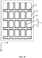
- FIG. 15 is a schematic plan view showing a second substrate of another display panel according to an exemplary embodiment of the present disclosure.
- FIG. 16 is a schematic plan view showing a second substrate of another display panel according to an exemplary embodiment of the present disclosure.
- FIG. 17 is a schematic diagram showing a circuit structure of an optical sensor in another display panel according to an exemplary embodiment of the present disclosure.
- FIG. 18 is a schematic cross-sectional structural view of another display panel according to an exemplary embodiment of the present disclosure.
- FIG. 19 is a schematic cross-sectional structural view of another display panel according to an exemplary embodiment of the present disclosure.
- a fingerprint of a finger FI has ridges 401 and valleys 402 .
- the ridges 401 are in contact with a surface of the display panel, and the valleys 402 are not in contact with the surface of the display panel, so that reflectance is different when light L is irradiated to the display panel corresponding to the valleys 402 and the ridges 401 of the fingerprint.
- intensity of reflected light received by the optical sensor D is different for reflected light formed at positions of the ridges 401 and reflected light formed at positions of the valleys 402 , correspondingly, magnitude of photocurrent in the optical sensor D is different for photocurrent converted from the reflected light formed at the positions of the ridges 401 and the reflected light formed at the positions of the valleys 402 .
- the magnitude of the photocurrent the ridges and the valleys of the fingerprint can be identified, and magnitude of currents from multiple optical sensors D is integrated to identify the fingerprint information.
- the present disclosure provides a display panel and a display device. Exemplary embodiments of the display panel and the display device provided by the present disclosure will be described in detail below.
- FIG. 2 is a schematic cross-sectional structural view of a display panel according to an exemplary embodiment of the present disclosure.
- One embodiment provides a display panel, including: a first substrate 100 , a second substrate 200 , and a liquid crystal layer 300 sandwiched between the first substrate 100 and the second substrate 200 .
- the first substrate 100 includes a first base substrate 110 and an optical sensor 20 disposed on the first base substrate 110 .
- the second substrate 200 includes a second base substrate 210 , a black matrix 30 disposed on the second base substrate 210 , and a light collecting structure 40 disposed on a side of the black matrix 30 adjacent to the first substrate 100 .
- the optical sensor 20 and the light collecting structure 40 overlap each other in a direction perpendicular to the display panel.
- the direction perpendicular to the display panel is direction Z shown in the drawing.
- the light collecting structure 40 includes at least one transparent protrusion 41 protruded along a direction perpendicular to a surface of the first substrate 100 or the second substrate 200 and from the second substrate 200 to the first substrate 100 .
- a refractive index of the light collecting structure 40 is larger than a refractive index of the liquid crystal layer 300 .
- the display panel provided in one embodiment is a liquid crystal display panel, and includes the first substrate 100 , the second substrate 200 , and the liquid crystal layer 300 .
- the first substrate 100 may be an array substrate, and the second substrate 200 may be a color film substrate.
- the liquid crystal layer 300 is sealed between the first substrate 100 and the second substrate 200 .
- the first substrate 100 includes the first base substrate 110 , which is typically a transparent material to avoid affecting transmittance of light.
- the first base substrate 110 may be flexible, for example, made of a resin material, or may be hard, for example, made of a glass material, which is not specifically limited in one embodiment.
- the first base substrate 110 is used to carry the optical sensor 20 .
- the optical sensor 20 is disposed on a side of the first base substrate 110 adjacent to the second substrate 200 only as an example.
- the optical sensor 20 may also be disposed on a side of the first base substrate 110 away from the second substrate 200 , which is not specifically limited in one embodiment.
- the optical sensor 20 is a photosensitive device that senses light and converts an optical signal into an electrical signal. Magnitude of the converted electrical signal varies with intensity of the light. The stronger the light, the larger the electrical current signal. The weaker the light, the smaller the electrical current signal.
- the second substrate 200 includes a second base substrate 210 , which is typically a transparent material to avoid affecting transmittance of light.
- the second base substrate 210 may be flexible, for example, made of a resin material, or may be hard, for example, made of a glass material, which is not specifically limited in one embodiment.
- the black matrix 30 is disposed on the second base substrate 210 .
- the black matrix has strong light absorbing capability, mainly preventing light leakage between pixels of the display panel (not shown), increasing contrast of color, and improving display effect.
- a color resist layer 50 may be disposed on the second base substrate 210 .
- the color resist layer 50 has a filtering effect.
- the color resist layer 50 may include color resists of at least three different colors.
- the display panel provided in one embodiment is provided with the light collecting structure 40 .
- the light collecting structure 40 has a function of converging light, which can increase intensity of light irradiated to the optical sensor 20 .
- the light collecting structure includes at least one transparent protrusion 41 which is made of a material having a high light transmittance, corresponds to a convex lens, and has a function of converging light.
- FIG. 3 is an optical path diagram of the display panel shown in FIG. 2 during fingerprint recognition.
- a fingerprint of a finger FI has ridges 401 and valleys 402 .
- the ridges 401 are in contact with a surface of the display panel, and the valleys 402 are not in contact with the surface of the display panel.
- light L is irradiated onto the surface of the display panel at the positions corresponding to the valleys 402 , reflectance is high, and partially reflected light sequentially passes through the second base substrate 210 and the color resist layer 50 , and then is irradiated to the light collecting structure 40 .
- the light collecting structure 40 converges the light.
- the optical sensor 20 and the light collecting structure 40 overlap each other in the direction Z, that is, the optical sensor 20 is located below the light collecting structure 40 and in a light emitting direction of the light converged by the light collecting structure 40 , thus the light converged by the light collecting structure 40 can be irradiated to the optical sensor 20 , thereby increasing the intensity of the light that is incident on the optical sensor 20 .
- the greater the intensity of the sensed light of the optical sensor 20 the more sensitive the optical sensor 20 , the larger the corresponding converted current signal.
- a larger current signal facilitates reception and recognition, and can improve the accuracy of fingerprint recognition.
- the refractive index of the light collecting structure 40 is set to be larger than the refractive index of the liquid crystal layer 300 .
- the light collecting structure 40 is made of a medium with a higher refractive index
- the liquid crystal layer 300 is made of a medium with a lower refractive index.
- FIG. 4 is an optical path diagram in the light collecting structure of the display panel shown in FIG. 2 .
- light L is irradiated to a surface of the display panel corresponding to the valleys 402 .
- reflectance is high.
- part of reflected light is irradiated to the light collecting structure 40 .
- the angle of refraction r is greater than the angle of incidence i, so that the emitted light is directed toward the optical sensor 20 , thereby facilitating the optical sensor 20 to receive more light.
- the refractive index of the light collecting structure 40 is N1, and 1.4 ⁇ N1 ⁇ 1.9.
- the refractive index of the liquid crystal layer 300 is usually less than 1.4, and a refractive index range of the light collecting structure 40 is set to be between about 1.4 and about 1.9.
- the refractive index of the light collecting structure 40 can be made larger than the refractive index of the liquid crystal layer 300 , and on the other hand, the refractive index of the light collecting structure 40 should not be too large, and a refractive index more than 1.9 may make the angle of refraction too large, which is disadvantageous for being received by the optical sensor.
- the light collecting structure 40 is disposed on the side of the black matrix 30 adjacent to the first substrate 100 , so that light converged by the light collecting structure 40 can be prevented from being absorbed by the black matrix 30 after being emitted.
- the black matrix 30 covers the light collecting structure 40 . Since the black matrix 30 has a function of absorbing light, no light is emitted from an area where the black matrix 30 is located.
- the light collecting structure 40 is disposed in a region where no light is emitted, so that the light collecting structure 40 can be prevented from affecting the normal light emission at other positions, thereby avoiding affecting transmittance of the display panel.
- the display panel provided in one embodiment has at least the following beneficial effects.
- the display panel includes a first substrate 100 , a second substrate 200 , and a liquid crystal layer 300 sandwiched between the first substrate 100 and the second substrate 200 .
- An optical sensor 20 is disposed in the first substrate 100 , and the optical sensor 20 is a photosensitive device that can convert an optical signal into an electrical signal.
- a black matrix 30 is disposed in the second substrate 200 , and a light collecting structure 40 is disposed on a side of the black matrix 30 adjacent to the first substrate 100 .
- the light collecting structure 40 has a function of converging light, and includes at least one transparent protrusion 41 .
- the at least one transparent protrusion 41 is made of a material having a high light transmittance, and is equivalent to a convex len to converge the light, thereby increasing intensity of light that is incident on the optical sensor 20 .
- the greater the intensity of the sensed light of the optical sensor 20 the more sensitive the optical sensor 20 , and the larger the corresponding converted current signal.
- a larger current signal facilitates reception and recognition, which improves the accuracy of fingerprint recognition and improves user experience.
- the light collecting structure includes at least one transparent protrusion 41
- FIGS. 2 and 3 only include one transparent protrusion 41 in the light collecting structure.
- the number of the transparent protrusion 41 may be two.
- FIG. 5 is a schematic cross-sectional structural view of another display panel according to an exemplary embodiment of the present disclosure.
- the number of the transparent protrusion 41 may be three or more, and may be set according to factors such as the size of the light collecting structure 40 and the sensitivity of the optical sensor 20 , and will not be further described in the embodiments of the present disclosure.
- FIG. 6 is a schematic cross-sectional structural view of another display panel according to one exemplary embodiment of the present disclosure
- FIG. 7 is a schematic cross-sectional structural view of another display panel according to one exemplary embodiment of the present disclosure.
- a vertical cross-section of the transparent protrusion 41 is a first pattern P 1 , and the vertical cross-section is perpendicular to a surface of the second base substrate 210 .
- the first pattern P 1 includes a sharp corner, and the sharp corner or a rounded corner protrudes toward the first substrate 100 .
- the first pattern P 1 can include a rounded corner, and the rounded corner protrudes toward the first substrate 100 .
- FIG. 6 and FIG. 7 illustrate the cross-sectional structure of the display panel, which is perpendicular to a surface of the second base substrate 210 .
- the vertical cross-section of the transparent protrusion 41 is illustrated in FIGS. 6 and 7 .
- the vertical cross-section of the transparent protrusion 41 is a planar figure, that is, the first pattern P 1 .
- the first pattern P 1 has a sharp corner or a rounded corner that is convex toward the first substrate 100 .
- the shape of the sharp corner or the rounded corner facilitates the convergence of the light, and the reflected light enters the light collecting structure 40 and exits toward the optical sensor 20 , thereby increasing the intensity of the light irradiated to the optical sensor 20 and improving the accuracy of fingerprint recognition.
- an angle of the sharp corner is ⁇ , 70° ⁇ 130°.
- the rounded corner includes a first side a 1 , a second side a 2 , and an arc a 3 connecting the first side a 1 and the second side a 2 .
- An angle between the first side a 1 and the second side a 2 is ⁇ , 70° ⁇ 130°.
- the first pattern P 1 may include a sharp corner or a rounded corner.
- the first pattern P 1 is difficult to form an absolute sharp angle due to limitations in the manufacturing process and the like, and is generally a rounded structure in the actually manufactured product.
- FIG. 8 is an optical path diagram of a light collecting structure in another display panel according to an exemplary embodiment of the present disclosure.
- FIG. 9 is an optical path diagram of a light collecting structure in another display panel according to an exemplary embodiment of the present disclosure.
- FIG. 10 is an optical path diagram of a light collecting structure in another display panel according to an exemplary embodiment of the present disclosure.
- ⁇ 70°
- the angle of emitted light after passing through the light collecting structure 40 is greater than ⁇ 80°, which is disadvantageous for being received by the optical sensor.
- the incident angle of the light is 40°-89°
- the angle of the emitted light passing through the light collecting structure 40 is 0°-29°, and the emitted light in this range is favored to be received by the optical sensor.
- ⁇ 90°
- the incident angle of the light is less than 10°
- total reflection occurs when the light enters the light collecting structure 40 .
- the angle of the emitted light passing through the light collecting structure 40 is ⁇ 35°, which is favorable for being received by the optical sensor.
- the incident angle of the light is 31°-89°
- the angle of the emitted light passing through the light collecting structure 40 is 0°-35°, and the emitted light in this range is favored to be received by the optical sensor.
- ⁇ 110°
- the angles of the emitted light after passing through the light collecting structure 40 are ⁇ 30°, 0°, and 41°, respectively.
- the emitted light is all favored to be received by the optical sensor.
- the arrow of the emitted light points to the upper side of the figure, and the angle of the emitted light is positive; the arrow of the emitted light points to the lower side of the figure, and the angle of the emitted light is negative.
- the positive and negative values of the emitted light angle are only for distinguishing the direction of the emitted light.
- the absolute value of the emitted light angle is compared.
- the rounded corner can be approximated to be a sharp angle
- the optical path diagram of the ⁇ angle of the light collecting structure can refer to FIG. 8 through FIG. 10 .
- FIG. 11 is a cross-sectional structural diagram of another display panel according to an exemplary embodiment of the present disclosure.
- the light collecting structure 40 includes a plurality of transparent protrusions 41 , and a recess 42 is between two adjacent transparent protrusions of the plurality of transparent protrusions 41 .
- a surface of the transparent protrusion 41 is a convex surface, and a surface of the recess 42 is a concave surface.
- the transparent protrusion 41 is convex toward the first substrate 100
- the recess 42 is concaved toward inside of the light collecting structure 40 .
- the surface of the transparent protrusion 41 and the surface of the recess 42 are curved structures, that is, a cross section of a side of the light collecting structure 40 facing the first substrate 100 shoves a wavy line.
- a surface of the light collecting structure 40 facing the first substrate 100 is curved, the shape is easy to manufacture, the requirement to the process precision is low, and the process difficulty can be reduced.
- FIGS. 6, 7, and 11 exemplarily describe a cross-sectional shape of the transparent protrusion 41 . It is to be understood that the shape of the transparent protrusion in the practice of the present disclosure is not limited thereto.
- FIG. 12 is a schematic cross-sectional view of another display panel according to an exemplary embodiment of the present disclosure.
- a side surface of a transparent protrusion 41 facing the first substrate 100 is spherical, that is, a cross section of the transparent protrusion 41 shown in FIG. 12 is an arc shape, and the transparent protrusion 41 is disposed in close proximity.
- the transparent protrusion 41 generally has a transition surface having a concave curved shape, and the actually manufactured product usually has the structure shown in FIG. 11 .
- the shape of the transparent protrusion 41 can also be various shapes, for example, an irregular shape, or any other suitable shape.
- the angle of the sharp corner is ⁇ , 70° ⁇ 130°.
- ⁇ should not be more than 130°, when it exceeds 130°, the light converging effect of the light collecting structure 40 is deteriorated, and the emitted light is disadvantageous for being received by the optical sensor. Therefore, in one embodiment shown in FIG. 6 , 70° ⁇ 130°, and a same incident light has an excellent converging effect.
- FIG. 13 is a cross-sectional structural diagram of another display panel according to an exemplary embodiment of the present disclosure.
- a reflective layer FL is disposed on a surface of the black matrix 30 away from the second base substrate 210 .
- the reflective layer FL has a high reflectance for light.
- it can be made of a metal material such as metallic silver.
- a metal material may be coated on a surface of the black matrix after the black matrix is completed, and then patterned to form the reflective layer FL.
- part of the light L passes through the first substrate 100 and the liquid crystal layer 300 , and is irradiated to the reflective layer FL.
- Part of the light reflected by the reflective layer FL is irradiated to the optical sensor 20 , thereby further increasing the light to the optical sensor 20 , improving the accuracy of fingerprint recognition, and improving user experience.
- FIG. 14 is a cross-sectional structural diagram of another display panel according to an exemplary embodiment of the present disclosure.
- the second substrate 200 further includes a color resist layer 50 and an insulating layer 60 .
- the color resist layer 50 is located on a side of the black matrix 30 adjacent to the first substrate 100
- the insulating layer 60 is located between the light collecting structure 40 and the color resist layer 50 .
- the color resist layer 50 includes a red color resist block 50 R, a green color resist block 50 G, and a blue color resist block 50 B.
- the insulating layer 60 has insulating properties and can protect the color resist 50 and the black matrix 30 on the other hand, the insulating layer 60 can smooth the step formed by the color resist 50 and the black matrix 30 .
- the insulating layer 60 may be made of an organic material or an inorganic material, which is not specifically limited in this embodiment.
- the second substrate 200 further includes a plurality of support pillars PS disposed on a side of the black matrix 30 adjacent to the first substrate 100 .
- the light collecting structure 40 and the plurality of support pillars PS are made of a same material and are located on a same film layer.
- the plurality of support pillars PS is located on a side of the insulating layer 60 adjacent to the first substrate 100 .
- the light collecting structure 40 can be fabricated in a same process as the plurality of support pillars PS.
- the light collecting structure 40 and the plurality of support pillars PS may be simultaneously formed by patterning a same material layer.
- the display panel provided in one embodiment is advantageous for reducing manufacturing process of the display panel and reducing cost.
- FIG. 15 is a schematic plan view showing a second substrate of another display panel according to an exemplary embodiment of the present disclosure.
- the display panel includes a display area AA and a non-display area NA surrounding the display area AA, and a portion of the black matrix 30 in the display area AA is a grid shape.
- the black matrix 30 includes a plurality of first portions 31 extending in a first direction X, and a plurality of second portions 32 extending in a second direction Y.
- the plurality of first portions 31 and the plurality of second portions 32 intersect.
- an orthographic projection of the light collecting structure 40 on the second base substrate 210 is a grid shape.
- FIG. 15 is a view obtained by observing the second substrate in a direction perpendicular to a surface of the second base substrate 210 , and thus, in FIG. 15 , an orthographic projection of the light collecting structure 40 on the second base substrate 210 overlaps the light collecting structure 40 , and the orthographic projection of the light collecting structure 40 on the second base substrate 210 is not otherwise illustrated in FIG. 15 .
- the light collecting structure 40 is arranged in a grid shape to increase the orthographic projection area of the light collecting structure 40 , so that the light collecting structure can collect reflected light from more positions, which is advantageous for increasing the light that is irradiated to the optical sensor, improving the accuracy of fingerprint recognition, and enhancing user experience.
- an orthographic projection of the black matrix 30 on the second base substrate 210 completely covers the orthographic projection of the light collecting structure 40 on the second base substrate 210 .
- the orthographic projection of the light collecting structure 40 on the second base substrate 210 is located within the orthographic projection range of the black matrix 30 on the second base substrate 210 . It should be noted that the orthographic projection of the black matrix 30 on the second base substrate 210 overlaps its own range, and the orthographic projection of the black matrix 30 on the second base substrate 210 is not separately illustrated in FIG. 15 .
- the light collecting structure 40 is disposed in the region where the black matrix is located, which can prevent the light collecting structure 40 from affecting the normal light emission in the opening region of the display panel, thereby avoiding affecting transmittance of the display panel.
- FIG. 16 is a schematic plan view of a second substrate of another display panel according to an exemplary embodiment of the present disclosure.
- a plurality of the light collecting structures 40 is provided, and an orthographic projection of the light collecting structure 40 on the second base substrate 210 is a strip shape.
- the orthographic projection of the light collecting structure 40 on the second base substrate 210 extends in a first direction X or in a second direction Y.
- specific number of the plurality of light collecting structures 40 can be set according to the actual requirements of the display panel, and each of the plurality of light collecting structures 40 is an independent structure.
- An orthographic projection of a light collecting structure 40 B on the second base substrate 210 may be a strip shape extending in the first direction X, or an orthographic projection of a light collecting structure 40 A on the second base substrate 210 may be a strip shape in the second direction Y.
- orthographic projections of light collecting structures in the display panel on the second base substrate 210 may all be strip shapes extending in the first direction X. In other embodiments, orthographic projections of the light collecting structures of the display panel on the second base substrate 210 may all be strip shapes extending in the second direction Y. In other embodiments, as shown in FIG. 16 , orthographic projections of some light collecting structures of the display panel on the second base substrate 210 are strip shapes extending in the first direction X, and orthographic projections of the other light collecting structures on the second base substrate 210 are strip shapes extending in the second direction Y. It can be understood that specific number and density of the light collecting structures can be set according to the actual situation of the display panel, which is not specifically limited in this embodiment.
- each light collecting structure is an independent structure, and may make space for another structure in the display panel.
- each light collecting structure as an independent structure can make space for the support pillars PS to prevent the light collecting structures from affecting the normal setting of the support pillars PS.
- FIG. 17 is a schematic structural diagram of a circuit of an optical sensor in another display panel according to an exemplary embodiment of the present disclosure.
- an optical sensor 20 includes a first switch 21 and a photodiode 22 , and the first switch 21 and the photodiode 22 are electrically connected.
- a gate 21 a of the first switch 21 receives a control signal for controlling whether the first switch is turned on or off.
- a first terminal 21 b of the first switch 21 receives a voltage signal.
- the optical sensor 20 further includes a capacitor DC.
- One electrode of the capacitor DC is electrically connected to a second terminal 21 c of the first switch 21 , and the other electrode is electrically connected to the photodiode 22 .
- a node H 1 inputs a low voltage signal, and the first terminal 21 b of the first switch 21 receives a high voltage signal.
- the entire fingerprint identification phase includes a preparation phase, a fingerprint signal acquisition phase, and a fingerprint signal detection phase.
- a control signal of the gate 21 a of the first switch 21 controls the first switch 21 of the optical sensor 20 to be turned on, and the capacitor DC is charged until the charging of the capacitor DC is completed.
- the first switch 21 controlling the optical sensor 20 is turned off.
- a user presses a finger on the display panel light irradiates to the finger and reflects on a surface of the finger fingerprint to form reflected light.
- the reflected light formed by the finger fingerprint reflection is incident on the optical sensor 20 , and is received by the photodiode 22 of the optical sensor 20 , to form a photocurrent with a direction from a node H 2 to the node H 1 , thereby causing the potential of the node H 2 to change.
- the amount of potential change of the node H 2 can be directly detected, thereby determining magnitude of the photocurrent.
- the first switch 21 of the optical sensor 20 can also be controlled to be turned on. At this time, there is a potential difference between the two electrodes of the capacitor DC, and the capacitor DC is in a charging state. The amount of charge charged by the capacitor DC can be detected to determine the magnitude of the photocurrent.
- FIG. 18 is a cross-sectional structural diagram of another display panel according to an exemplary embodiment of the present disclosure.
- the first substrate 100 further includes: an array layer 120 disposed on a side of the first base substrate 110 adjacent to the second substrate 200 , a planarization layer PLN, a pixel electrode layer 130 , and a common electrode layer 140 .
- the array layer 120 includes a plurality of thin film transistors ST.
- An optical sensor 20 is located on a side of the first base substrate 110 away from the second substrate 200 .
- the first substrate 100 is an array substrate.
- the array layer 120 may be provided with signal traces (not shown) in addition to the plurality of thin film transistors ST.
- the planarization layer PLN generally includes an organic material to smooth out the step formed by the plurality of thin film transistors ST.
- FIG. 18 an embodiment in which the pixel electrode layer 130 is located on a side of the common electrode layer 140 adjacent to the first base substrate 110 is illustrated. Alternatively, the common electrode layer 140 may also be located on a side of the pixel electrode layer 130 adjacent to the first base substrate 110 .
- the optical sensor 20 is disposed on a side of the first base substrate 110 away from the second substrate 200 , and the optical sensor 20 is fabricated after the film layers on the side of the first base substrate 110 adjacent to the second substrate 200 are completed. So that the manufacturing process of the array layer 120 , the planarization layer PLN, the pixel electrode layer 130 , and the common electrode layer 140 don't need to be changed, which is advantageous for reducing the manufacturing cost of the display panel.
- FIG. 19 is a cross-sectional structural diagram of another display panel according to an exemplary embodiment of the present disclosure.
- the first substrate 100 further includes: an array layer 120 disposed on a side of the first base substrate 110 adjacent to the second substrate 200 , a planarization layer PLN, a pixel electrode layer 130 , and a common electrode layer 140 .
- the array layer 120 includes a plurality of thin film transistors ST.
- An optical sensor 20 includes: a first switch 21 and a photodiode 22 .
- the first switch 21 is located in the array layer 120 .
- the photodiode 22 includes a PN junction, and the PN junction includes an N-type semiconductor region 22 N and a P-type semiconductor region 22 P.
- An active layer 21 d of the first switch 21 is multiplexed into the N-type semiconductor region 22 N.
- the P-type semiconductor region 22 P is located on a side surface of the N-type semiconductor region 22 N away from the first base substrate 110 .
- the first substrate 100 is an array substrate, and a plurality of thin film transistors ST is disposed in the array layer 120 . In one embodiment, only one of the plurality of thin film transistors ST is illustrated to illustrate the film structure of the first substrate 100 . It is to be understood that the specific number of the plurality of thin film transistors ST needs to be set according to the actual requirements of the display panel, which is not specifically limited in this embodiment.
- the optical sensor 20 includes the photodiode 22 , and the core component of the photodiode 22 is the PN junction.
- the PN junction is formed by closely contacting an N-type doping region (i.e., the N-type semiconductor region 22 N) and a P-type doping region (i.e., the P-type semiconductor region 22 P).
- the PN junction has photosensitive properties and has unidirectional conductivity. When there is no light, the PN junction has a small saturated reverse leakage current, that is, a dark current, at which time the photodiode is turned off. When exposed to light, the saturated reverse leakage current of the PN junction is greatly increased, to form a current. The current strength varies with the intensity of the incident light.
- the optical sensor 20 further includes the first switch 21 including a gate 21 a , a source 21 b , a drain 21 c , and the active layer 21 d .
- the active layer 21 d is lengthened and multiplexed into the N-type semiconductor region 22 N of the PN junction.
- the active layer 21 d is extended to a side of the P-type semiconductor region 22 P close to the first base substrate 110 and electrically connected to the P-type semiconductor region 22 P, thereby reducing the process for fabricating the optical sensor and facilitating the thinness of the display panel.
- the first switch 21 is located on the array layer 120 and can be fabricated simultaneously with the plurality of thin film transistors ST, which can further reduce the process for fabricating the optical sensor.
- the common electrode layer 140 and the P-type semiconductor region 22 P are electrically connected for supplying a voltage signal to the PN junction.
- the display panel provided in one embodiment integrates the optical sensor 20 in the first substrate, which is beneficial to reduce the process of the display panel. It also contributes to the thinness of the display panel. Moreover, the optical sensor 20 is located on a side of the first base substrate 110 close to the second substrate 200 , and is closer to the light collecting structure 40 , which is favorable for receiving the light emitted from the light collecting structure 40 , and reducing the loss during transmission of the light emitted from the light collecting structure 40 , thereby increasing the light received by the optical sensor 20 , improving the accuracy of fingerprint recognition, and improving the user experience.
- One embodiment of the present disclosure further provides a display device, including the display panel provided by any of the above embodiments of the present disclosure.
- FIG. 20 is a schematic structural diagram of a display device according to an exemplary embodiment of the present disclosure.
- a display device 1000 provided in FIG. 20 includes a display panel 1001 provided by any of the above embodiments of the present disclosure.
- One embodiment of the present disclosure is a description of the display device 1000 by using a mobile phone as an example.
- the display device provided by the embodiment of the present disclosure may be a computer, a television, an in-vehicle display device, or the like, having other display functions and fingerprint recognition functions.
- the display device is not specifically limited in the present disclosure.
- the display device provided by the embodiment of the present disclosure has the beneficial effects of the display panel provided by the embodiments of the present disclosure. For details, refer to the detailed description of the display panel in the foregoing embodiments, and details are not described herein again.
- the display panel and the display device provided by the present disclosure achieve at least the following beneficial effects.
- the display panel includes a first substrate, a second substrate, and a liquid crystal layer sandwiched between the first substrate and the second substrate.
- An optical sensor is disposed in the first substrate, and the optical sensor is a photosensitive device and can convert an optical signal into an electrical signal.
- a black matrix is disposed in the second substrate, and a light collecting structure is disposed on a side of the black matrix adjacent to the first substrate.
- the light collecting structure has a function of converging light, and includes at least one transparent protrusion.
- the at least one transparent protrusion is made of a material having a high light transmittance, is equivalent to a convex lens, and has a function of converging light to increase light intensity of light irradiated to the optical sensor. The greater the intensity of the sensed light of the optical sensor, the more sensitive the optical sensor, and the larger the corresponding converted current signal.
- a larger current signal facilitates reception and recognition, which improves the accuracy of fingerprint recognition and improves the user experience.
Landscapes
- Physics & Mathematics (AREA)
- Engineering & Computer Science (AREA)
- Nonlinear Science (AREA)
- General Physics & Mathematics (AREA)
- Mathematical Physics (AREA)
- Chemical & Material Sciences (AREA)
- Crystallography & Structural Chemistry (AREA)
- Optics & Photonics (AREA)
- Theoretical Computer Science (AREA)
- Multimedia (AREA)
- Human Computer Interaction (AREA)
- General Engineering & Computer Science (AREA)
- Microelectronics & Electronic Packaging (AREA)
- Devices For Indicating Variable Information By Combining Individual Elements (AREA)
- Liquid Crystal (AREA)
Abstract
Description
Claims (18)
Applications Claiming Priority (2)
| Application Number | Priority Date | Filing Date | Title |
|---|---|---|---|
| CN201811610169.3 | 2018-12-27 | ||
| CN201811610169.3A CN109447046B (en) | 2018-12-27 | 2018-12-27 | Display panels and display devices |
Publications (2)
| Publication Number | Publication Date |
|---|---|
| US20200209679A1 US20200209679A1 (en) | 2020-07-02 |
| US11150505B2 true US11150505B2 (en) | 2021-10-19 |
Family
ID=65538263
Family Applications (1)
| Application Number | Title | Priority Date | Filing Date |
|---|---|---|---|
| US16/433,918 Active 2039-12-20 US11150505B2 (en) | 2018-12-27 | 2019-06-06 | Display panel and display device |
Country Status (2)
| Country | Link |
|---|---|
| US (1) | US11150505B2 (en) |
| CN (1) | CN109447046B (en) |
Cited By (1)
| Publication number | Priority date | Publication date | Assignee | Title |
|---|---|---|---|---|
| US12175789B2 (en) | 2021-10-28 | 2024-12-24 | Honor Device Co., Ltd. | Module integrated with optical sensor, display panel, and display apparatus |
Families Citing this family (18)
| Publication number | Priority date | Publication date | Assignee | Title |
|---|---|---|---|---|
| CN110068947A (en) * | 2019-04-02 | 2019-07-30 | 惠科股份有限公司 | Display panel and display device |
| CN113330576A (en) * | 2019-05-24 | 2021-08-31 | 深圳市柔宇科技股份有限公司 | Display panel and electronic device |
| CN112036212B (en) * | 2019-06-03 | 2024-11-19 | 群创光电股份有限公司 | Electronic Devices |
| CN110348309B (en) * | 2019-06-11 | 2022-04-01 | 惠科股份有限公司 | Optical fingerprint sensor and display screen |
| US11288486B2 (en) * | 2019-06-12 | 2022-03-29 | Lms Co., Ltd. | Fingerprint recognition optical film, and backlight unit and liquid crystal display device comprising the film optical |
| CN110245631B (en) * | 2019-06-20 | 2021-09-21 | 厦门天马微电子有限公司 | Display panel and fingerprint identification display device |
| CN110135405B (en) * | 2019-06-26 | 2023-03-10 | 京东方科技集团股份有限公司 | Fingerprint recognition module, array substrate and manufacturing method thereof, and liquid crystal display panel |
| CN110376788B (en) * | 2019-07-31 | 2022-04-05 | 厦门天马微电子有限公司 | Display panel and display device |
| US20210110131A1 (en) * | 2019-10-09 | 2021-04-15 | Novatek Microelectronics Corp. | Fingerprint recognition apparatus |
| CN110728266A (en) * | 2019-10-30 | 2020-01-24 | 维沃移动通信(杭州)有限公司 | Display module and electronic equipment |
| CN110928032B (en) * | 2019-12-13 | 2021-09-24 | 武汉华星光电技术有限公司 | Liquid crystal display panel and liquid crystal display device |
| WO2022033920A1 (en) * | 2020-08-14 | 2022-02-17 | Ams International Ag | Sensor module |
| CN112946945A (en) * | 2020-12-31 | 2021-06-11 | 武汉华星光电技术有限公司 | Display panel and display device |
| CN114815364B (en) * | 2021-01-18 | 2023-11-21 | 北京小米移动软件有限公司 | Display screen and manufacturing method and terminal thereof |
| CN113641031B (en) * | 2021-08-30 | 2022-07-01 | 厦门天马微电子有限公司 | Array substrate, display panel and display device |
| CN116137898A (en) * | 2021-09-17 | 2023-05-19 | 京东方科技集团股份有限公司 | Display panel, manufacturing method thereof, and display device |
| CN114596596B (en) * | 2022-03-07 | 2025-08-26 | 合肥维信诺科技有限公司 | Display module and display device |
| CN114998948B (en) * | 2022-06-08 | 2026-01-20 | 京东方科技集团股份有限公司 | Fingerprint recognition substrate and display device having it |
Citations (6)
| Publication number | Priority date | Publication date | Assignee | Title |
|---|---|---|---|---|
| US20070182890A1 (en) * | 2006-02-08 | 2007-08-09 | Seiko Epson Corporation | Liquid crystal device and projector |
| US20090225538A1 (en) * | 2005-06-29 | 2009-09-10 | Kuraray Co., Ltd. | Lighting device and light control member used for this and image display unit using these |
| CN105868742A (en) | 2016-05-26 | 2016-08-17 | 京东方科技集团股份有限公司 | Display unit and display device |
| CN106295527A (en) | 2016-07-29 | 2017-01-04 | 京东方科技集团股份有限公司 | A kind of array base palte, display floater, display device and method of work |
| CN108983506A (en) | 2018-07-20 | 2018-12-11 | 上海中航光电子有限公司 | Display panel and display device |
| US20190331948A1 (en) * | 2018-09-05 | 2019-10-31 | Shanghai Tianma Micro-electronics Co., Ltd. | Liquid crystal display panel and 3d printer |
Family Cites Families (7)
| Publication number | Priority date | Publication date | Assignee | Title |
|---|---|---|---|---|
| CN102707504B (en) * | 2011-11-21 | 2016-04-27 | 京东方科技集团股份有限公司 | Liquid crystal panel and preparation method thereof, display device |
| CN102707470B (en) * | 2012-04-01 | 2015-06-03 | 京东方科技集团股份有限公司 | Liquid crystal panel, liquid crystal display and manufacturing method |
| US10410037B2 (en) * | 2015-06-18 | 2019-09-10 | Shenzhen GOODIX Technology Co., Ltd. | Under-screen optical sensor module for on-screen fingerprint sensing implementing imaging lens, extra illumination or optical collimator array |
| CN205942207U (en) * | 2016-05-17 | 2017-02-08 | 京东方科技集团股份有限公司 | Display panel and display device |
| CN106353944A (en) * | 2016-11-04 | 2017-01-25 | 京东方科技集团股份有限公司 | Array base plate, manufacturing method of array base plate, display panel and display device |
| CN107357130B (en) * | 2017-09-07 | 2021-04-27 | 京东方科技集团股份有限公司 | Mask, lens array and preparation method thereof, and display panel |
| CN109061948B (en) * | 2018-10-30 | 2021-02-12 | 京东方科技集团股份有限公司 | Optical substrate and display device |
-
2018
- 2018-12-27 CN CN201811610169.3A patent/CN109447046B/en active Active
-
2019
- 2019-06-06 US US16/433,918 patent/US11150505B2/en active Active
Patent Citations (6)
| Publication number | Priority date | Publication date | Assignee | Title |
|---|---|---|---|---|
| US20090225538A1 (en) * | 2005-06-29 | 2009-09-10 | Kuraray Co., Ltd. | Lighting device and light control member used for this and image display unit using these |
| US20070182890A1 (en) * | 2006-02-08 | 2007-08-09 | Seiko Epson Corporation | Liquid crystal device and projector |
| CN105868742A (en) | 2016-05-26 | 2016-08-17 | 京东方科技集团股份有限公司 | Display unit and display device |
| CN106295527A (en) | 2016-07-29 | 2017-01-04 | 京东方科技集团股份有限公司 | A kind of array base palte, display floater, display device and method of work |
| CN108983506A (en) | 2018-07-20 | 2018-12-11 | 上海中航光电子有限公司 | Display panel and display device |
| US20190331948A1 (en) * | 2018-09-05 | 2019-10-31 | Shanghai Tianma Micro-electronics Co., Ltd. | Liquid crystal display panel and 3d printer |
Cited By (1)
| Publication number | Priority date | Publication date | Assignee | Title |
|---|---|---|---|---|
| US12175789B2 (en) | 2021-10-28 | 2024-12-24 | Honor Device Co., Ltd. | Module integrated with optical sensor, display panel, and display apparatus |
Also Published As
| Publication number | Publication date |
|---|---|
| CN109447046A (en) | 2019-03-08 |
| US20200209679A1 (en) | 2020-07-02 |
| CN109447046B (en) | 2021-07-23 |
Similar Documents
| Publication | Publication Date | Title |
|---|---|---|
| US11150505B2 (en) | Display panel and display device | |
| US10665631B1 (en) | Display panel and display device | |
| US11144744B2 (en) | Backlight module, under-screen fingerprint identification apparatus and electronic device | |
| US11482051B2 (en) | Display apparatus and pattern identification method thereof | |
| US11804509B2 (en) | Fingerprint detection apparatus and electronic device | |
| US10417473B2 (en) | Optical imaging system with variable light field for biometrics application | |
| US10671830B2 (en) | Array substrate, display panel and display device | |
| US10810397B2 (en) | Display panel and display device | |
| TWI612647B (en) | Optoelectric sensor | |
| CN112236774B (en) | Texture recognition device and driving method of texture recognition device | |
| CN107422920B (en) | Array substrate and display panel | |
| WO2018126644A1 (en) | Fingerprint recognition apparatus and electronic device | |
| CN106055162A (en) | Display assembly and display device | |
| CN110718565A (en) | Display panel and display device | |
| CN209327746U (en) | Display components and electronic equipment | |
| CN106971181B (en) | Display panel and display device | |
| US12198461B2 (en) | Display panel and display device | |
| CN111812900B (en) | Display device and control method thereof | |
| WO2021217325A1 (en) | Texture recognition apparatus and opposite substrate | |
| CN110068947A (en) | Display panel and display device | |
| WO2018029442A1 (en) | Touch screen display | |
| CN110287920B (en) | Display panel and display device | |
| US10884273B1 (en) | Display panel comprising a photosensitive component that receives reflected light of a fingerprint and is connected to an underside of a second thin film transistor layer and display device | |
| CN210573815U (en) | Electronic device | |
| CN107609542A (en) | Light sensitive device, display device and fingerprint identification method |
Legal Events
| Date | Code | Title | Description |
|---|---|---|---|
| AS | Assignment |
Owner name: XIAMEN TIANMA MICRO-ELECTRONICS CO., LTD., CHINA Free format text: ASSIGNMENT OF ASSIGNORS INTEREST;ASSIGNORS:LING, ANKAI;CAI, XUANXIAN;ZHENG, BINYI;AND OTHERS;REEL/FRAME:049408/0164 Effective date: 20190531 |
|
| FEPP | Fee payment procedure |
Free format text: ENTITY STATUS SET TO UNDISCOUNTED (ORIGINAL EVENT CODE: BIG.); ENTITY STATUS OF PATENT OWNER: LARGE ENTITY |
|
| STPP | Information on status: patent application and granting procedure in general |
Free format text: DOCKETED NEW CASE - READY FOR EXAMINATION |
|
| STPP | Information on status: patent application and granting procedure in general |
Free format text: NON FINAL ACTION MAILED |
|
| STPP | Information on status: patent application and granting procedure in general |
Free format text: RESPONSE TO NON-FINAL OFFICE ACTION ENTERED AND FORWARDED TO EXAMINER |
|
| STPP | Information on status: patent application and granting procedure in general |
Free format text: FINAL REJECTION MAILED |
|
| STPP | Information on status: patent application and granting procedure in general |
Free format text: RESPONSE AFTER FINAL ACTION FORWARDED TO EXAMINER |
|
| STPP | Information on status: patent application and granting procedure in general |
Free format text: ADVISORY ACTION MAILED |
|
| STPP | Information on status: patent application and granting procedure in general |
Free format text: DOCKETED NEW CASE - READY FOR EXAMINATION |
|
| STPP | Information on status: patent application and granting procedure in general |
Free format text: NOTICE OF ALLOWANCE MAILED -- APPLICATION RECEIVED IN OFFICE OF PUBLICATIONS |
|
| STPP | Information on status: patent application and granting procedure in general |
Free format text: PUBLICATIONS -- ISSUE FEE PAYMENT VERIFIED |
|
| STCF | Information on status: patent grant |
Free format text: PATENTED CASE |
|
| MAFP | Maintenance fee payment |
Free format text: PAYMENT OF MAINTENANCE FEE, 4TH YEAR, LARGE ENTITY (ORIGINAL EVENT CODE: M1551); ENTITY STATUS OF PATENT OWNER: LARGE ENTITY Year of fee payment: 4 |