US11139792B2 - Method of tuning a radio frequency (RF) module including a non-volatile tunable RF filter - Google Patents
Method of tuning a radio frequency (RF) module including a non-volatile tunable RF filter Download PDFInfo
- Publication number
- US11139792B2 US11139792B2 US16/775,625 US202016775625A US11139792B2 US 11139792 B2 US11139792 B2 US 11139792B2 US 202016775625 A US202016775625 A US 202016775625A US 11139792 B2 US11139792 B2 US 11139792B2
- Authority
- US
- United States
- Prior art keywords
- pcm
- volatile
- switch
- filter
- tunable
- Prior art date
- Legal status (The legal status is an assumption and is not a legal conclusion. Google has not performed a legal analysis and makes no representation as to the accuracy of the status listed.)
- Active
Links
Images


Classifications
-
- H—ELECTRICITY
- H03—ELECTRONIC CIRCUITRY
- H03H—IMPEDANCE NETWORKS, e.g. RESONANT CIRCUITS; RESONATORS
- H03H7/00—Multiple-port networks comprising only passive electrical elements as network components
- H03H7/01—Frequency selective two-port networks
- H03H7/0115—Frequency selective two-port networks comprising only inductors and capacitors
-
- H—ELECTRICITY
- H03—ELECTRONIC CIRCUITRY
- H03H—IMPEDANCE NETWORKS, e.g. RESONANT CIRCUITS; RESONATORS
- H03H7/00—Multiple-port networks comprising only passive electrical elements as network components
- H03H7/01—Frequency selective two-port networks
- H03H7/0153—Electrical filters; Controlling thereof
- H03H7/0161—Bandpass filters
-
- H—ELECTRICITY
- H03—ELECTRONIC CIRCUITRY
- H03H—IMPEDANCE NETWORKS, e.g. RESONANT CIRCUITS; RESONATORS
- H03H7/00—Multiple-port networks comprising only passive electrical elements as network components
- H03H7/01—Frequency selective two-port networks
- H03H7/12—Bandpass or bandstop filters with adjustable bandwidth and fixed centre frequency
-
- H—ELECTRICITY
- H03—ELECTRONIC CIRCUITRY
- H03H—IMPEDANCE NETWORKS, e.g. RESONANT CIRCUITS; RESONATORS
- H03H7/00—Multiple-port networks comprising only passive electrical elements as network components
- H03H7/01—Frequency selective two-port networks
- H03H7/17—Structural details of sub-circuits of frequency selective networks
- H03H7/1741—Comprising typical LC combinations, irrespective of presence and location of additional resistors
- H03H7/1766—Parallel LC in series path
-
- H—ELECTRICITY
- H04—ELECTRIC COMMUNICATION TECHNIQUE
- H04B—TRANSMISSION
- H04B1/00—Details of transmission systems, not covered by a single one of groups H04B3/00 - H04B13/00; Details of transmission systems not characterised by the medium used for transmission
- H04B1/06—Receivers
- H04B1/16—Circuits
- H04B1/1638—Special circuits to enhance selectivity of receivers not otherwise provided for
-
- H—ELECTRICITY
- H04—ELECTRIC COMMUNICATION TECHNIQUE
- H04B—TRANSMISSION
- H04B17/00—Monitoring; Testing
- H04B17/20—Monitoring; Testing of receivers
- H04B17/21—Monitoring; Testing of receivers for calibration; for correcting measurements
-
- H—ELECTRICITY
- H03—ELECTRONIC CIRCUITRY
- H03H—IMPEDANCE NETWORKS, e.g. RESONANT CIRCUITS; RESONATORS
- H03H2210/00—Indexing scheme relating to details of tunable filters
- H03H2210/03—Type of tuning
- H03H2210/036—Stepwise
Definitions
- PCM Phase-Change Material
- RF Radio Frequency
- Radio frequency (RF) amplification techniques in semiconductor dies and products may employ filters and passive components to reject or suppress undesired frequencies, such as second or higher harmonics, that are often undesirably produced during amplification of a desired frequency, e.g. a fundamental frequency.
- filters and passive components exhibit variations associated with factory fabrication, which can result in failure to reject or suppress the undesired frequencies.
- the filter may be incompatible with regulatory requirements related to spurious emissions, and the semiconductor die or product may have to be discarded by the factory.
- switches can be used to reconfigure or time an individual RF filter to suppress undesired frequencies, such as harmonics.
- conventional switches are typically volatile and do not maintain their states during power off. Once the product utilizing the RF filter, e.g. a mobile phone, is in possession of an end-user, keeping power on at all times would be impractical and would also drain the battery. Conventional switches may also be unreliable and vary over time.
- fuses can be used to reconfigure a circuit.
- conventional fuses introduce significant electrical resistance, are too large, and introduce insertion losses that can prohibit RF filtering as intended.
- Conventional fuses are also one-time-programmable and cannot be reconfigured or re-used.
- the present disclosure is directed to a radio frequency (RF) module using a tunable RF filter with non-volatile RF switches, substantially as shown in and/or described in connection with at least one of the figures, and as set forth in the claims.
- RF radio frequency
- FIG. 1 illustrates a portion of a radio frequency (RF) module including an RF filter according to one implementation of the present application.
- RF radio frequency
- FIG. 2 illustrates a portion of an RF module including a non-volatile tunable RF filter employing non-volatile RF switches according to one implementation of the present application.
- FIG. 3 illustrates a perspective view of a portion of a phase-change material (PCM) RF switch according to one implementation of the present application.
- PCM phase-change material
- FIG. 4 is a flowchart of an exemplary method for tuning an RF module having a non-volatile tunable RF filter according to one implementation of the present application.
- FIG. 5 illustrates a portion of an RF module and a corresponding frequency response graph processed in accordance with the flowchart in FIG. 4 according to one implementation of the present application.
- FIG. 6 illustrates a portion of an RF module processed in accordance with the flowchart in FIG. 4 according to one implementation of the present application.
- FIG. 7 illustrates a portion of an RF module and a corresponding frequency response graph processed in accordance with the flowchart in FIG. 4 according to one implementation of the present application.
- FIG. 8 illustrates a portion of an RF module including a non-volatile tunable RF filter employing an adjustable capacitor according to one implementation of the present application.
- FIG. 9 illustrates a portion of an adjustable capacitor employing PCM RF switches according to one implementation of the present application.
- FIG. 1 illustrates a portion of a radio frequency (RF) module including an RF filter according to one implementation of the present application.
- the RF module includes RF input 102 , amplifier 104 having output 106 , RF filter 108 , and RF module output 122 .
- RF filter 108 includes fixed capacitors 110 , 112 , 118 , and 120 , and fixed inductor 114 .
- RF module output 122 is coupled to antenna 124 .
- Amplifier 104 amplifies RF signals received at RF input 102 .
- amplifier 104 can be coupled to a mixer of a transmit chain (not shown in FIG. 1 ), or to another input source.
- Output 106 of amplifier 104 is coupled to RF filter 108 .
- Amplifier 104 may be an operational amplifier and may comprise bipolar transistors and/or field effect transistors, or may be any other type of amplifier known in the art.
- amplifier 104 can be a power amplifier module for a consumer electronic device.
- amplifier 104 and can include multiple stages of amplifiers each providing a gain to the RF signals, multiple matching networks providing impedance matching between the amplifiers, and a bias controller for biasing the amplifiers.
- RF filter 108 is designed to pass desired frequencies output by amplifier 104 and to reject undesired frequencies output by amplifier 104 .
- RF filter 108 can be designed to substantially pass fundamental frequencies between five gigahertz and six gigahertz (5 GHz-6 GHz), and to substantially reject second harmonic frequencies between ten gigahertz and twelve gigahertz (10 GHz-12 GHz).
- RF filter 108 can be designed to pass and/or reject any other frequencies.
- RF filter 108 includes fixed capacitors 110 , 112 , 118 , and 120 , and fixed inductor 114 .
- Fixed capacitor 110 is coupled between output 106 of amplifier 104 and ground.
- Fixed capacitor 112 is coupled between output 106 of amplifier 104 and node 116 .
- Fixed inductor 114 is also coupled between output 106 of amplifier 104 and node 116 .
- Fixed capacitor 118 is coupled between node 116 and ground.
- Fixed capacitor 120 is coupled between node 116 and output 122 of the RF module.
- FIG. 1 illustrates one possible arrangement of RF filter 108 .
- RF filter 108 can include more or fewer inductors, capacitors, and/or resistors having various values and various arrangements.
- the RF module in FIG. 1 can be implemented in a consumer electronic device dial also includes antenna 124 .
- the consumer electronic device can be a mobile phone, a tablet, or another personal wireless communication device.
- Output 122 of the RF module is coupled to antenna 124 .
- Antenna 124 can transmit amplified and filtered RF signals output by the RF module.
- output 122 of the RF module can be coupled to an antenna array, rather than a single antenna 124 .
- a receive/transmit block can lie arranged between RF module output 122 and antenna 124 , in order to switch between receive and transmit modes.
- RF filter 108 can fail to substantially reject undesired frequencies.
- RF filter 108 may have been designed to substantially pass fundamental frequencies between five gigahertz and six gigahertz (5 GHz-6 GHz), and to substantially reject second harmonic frequencies between ten gigahertz and twelve gigahertz (10 GHz-12 GHz).
- the desired frequencies may correspond to fundamental frequencies in a wireless communication standard, such as a wireless local area network (WLAN) standard, a long-term evolution (LTE) standard, a 4G standard, or a 5G standard.
- WLAN wireless local area network
- LTE long-term evolution
- 4G 4G standard
- 5G 5G standard
- any of fixed capacitors 110 , 112 , 118 , and 120 may have a tolerance of ⁇ 20%, such that their actual capacitance values vary up to 20% from their nominal capacitance values.
- the frequency response of RF filter 108 correspondingly varies.
- RF filter 108 may fail to substantially pass all desired frequencies and/or may fail to substantially reject all undesired frequencies.
- substantially passing a frequency refers to an output RF signal having a high relative power at that frequency.
- substantially rejecting a frequency refers to an output RF signal having a low relative power at that frequency.
- the relative power can be relative to an input power, relative to a normalized power, or relative to a threshold power.
- RF Filter 108 may fail to substantially pass the desired frequencies when RF signals between five gigahertz and six gigahertz (5 GHz-6 GHz) have power below negative fifteen decibel-milliwatts ( ⁇ 15 dBm).
- RF filter 108 may fail to substantially reject undesired frequencies when RF signals between ten gigahertz and twelve gigahertz (10 GHz-12 GHz) have power above negative forty-two decibel-milliwatts ( ⁇ 42 dBm).
- antenna 124 may transmit harmonic frequencies output by the RF module having emission strengths that do not comply with United States regulatory requirements established by the Federal Communications Commission.
- semiconductor dies, products and consumer electronic devices using the non-compliant RF module may have to be discarded at the factory, reducing die or product yield.
- most of semiconductor dies, products and consumer electronic devices using a non-compliant RF module in a given production batch may have to be discarded.
- FIG. 2 illustrates a portion of an RF module including a non-volatile tunable RF filter employing non-volatile RF switches according to one implementation of the present application.
- the RF module includes RF input 102 , amplifier 104 having output 106 , non-volatile tunable RF filter 126 , and RF module output 122 .
- Non-volatile tunable RF filter 126 includes fixed capacitors 110 and 120 , adjustable capacitors 128 and 132 , and adjustable inductor 130 .
- Output 122 of the RF module is coupled to antenna 124 .
- non-volatile tunable RF filter 126 includes adjustable capacitors 128 and 132 .
- Adjustable capacitor 128 includes non-volatile RF switches 134 a , 134 b , and 134 c and fixed capacitors 136 a , 136 b , and 136 c .
- Non-volatile RF switches 134 a , 134 b , and 134 c are coupled between the output 106 of amplifier 104 and respective fixed capacitors 136 a , 136 b , and 136 c .
- Fixed capacitors 136 a , 136 b , and 136 c are coupled between respective non-volatile RF switches 134 a , 134 b , and 134 c and node 116 .
- adjustable capacitor 132 includes non-volatile RF switches 138 a , 138 b , and 138 c and fixed capacitors 140 a , 140 b , and 140 c .
- Non-volatile RF switches 138 a , 138 b , and 138 c are coupled between node 116 and respective fixed capacitors 140 a , 140 b , and 140 c .
- Non-volatile RF switches 134 a , 134 b , 134 c , 138 a , 138 b , and 138 c are phase-change material (PCM) RF switches.
- PCM phase-change material
- non-volatile RF switches 134 a , 134 b , 134 c , 138 a , 138 b , and 138 c can be any non-volatile switch known in the art.
- Adjustable capacitor 128 can be adjusted when non-volatile RF switches 134 a , 134 b , and 134 c are in ON states or OFF states. For example, when non-volatile RF switch 134 a is in an ON state, fixed capacitor 136 a is engaged and a first capacitance value can be achieved by adjustable capacitor 128 . Likewise, when non-volatile RF switch 134 b or 134 c is in an ON state, fixed capacitor 136 b or 136 c is engaged and second or third capacitance values can be achieved by adjustable capacitor 128 .
- adjustable capacitor 132 can be adjusted when non-volatile RF switches 138 a , 138 b , and 138 c are in ON states or OFF states, where fixed capacitors 140 a , 140 b , and 140 c are engaged or disengaged.
- “engaged” refers to having a very low resistance electrical connection to other parts of a circuit through a connecting non-volatile RF switch, e.g., when non-volatile RF switches 134 a , 134 b , and 134 c in the paths of fixed capacitors 136 a , 136 b , and 136 c are in ON (very low resistance) states. Further, “disengaged” refers to when non-volatile RF switches 134 a , 134 b , and 134 c are in OFF (very high resistance) states.
- fixed capacitors 136 a , 136 b , 136 c , 140 a , 140 b , and 140 c can have the same nominal capacitance values as each other or different nominal capacitance values.
- adjustable capacitors 128 and 132 can have more or fewer than three fixed capacitors each.
- fixed capacitors 136 a , 136 b , 136 c , 140 a , 140 b , and 140 c can be concurrently engaged by two corresponding non-volatile RF switches.
- a non-volatile RF switch can be coupled to more than one fixed capacitor.
- adjustable inductor 130 can be implemented using non-volatile RF switches and fixed inductors (not shown in FIG. 2 ).
- Non-volatile tunable RF Filter 126 can include more or fewer adjustable capacitors and/or adjustable inductors having various arrangements.
- non-volatile tunable RF filter 126 in FIG. 2 is tunable after fabrication. That is, adjustable capacitors 128 and 132 can be adjusted even after fabrication of non-volatile tunable RF filter 126 by changing states of non-volatile RF switches 134 a , 134 b , 134 c , 138 a , 138 b , and 138 c . Where fixed capacitors 112 and 118 in FIG. 1 may cause RF filter 108 to fail to substantially pass desired frequencies (e.g. a fundamental frequency) and/or fail to substantially reject undesired frequencies (e.g., a second harmonic frequency), adjustable capacitors 128 and 132 in FIG.
- desired frequencies e.g. a fundamental frequency
- undesired frequencies e.g., a second harmonic frequency
- non-volatile tunable RF filter 126 can be adjusted even after fabrication of the RF filter such that non-volatile tunable RF filter 126 substantially passes desired frequencies and substantially rejects undesired frequencies.
- non-volatile tunable RF filter 126 overcomes difficulties associated with process variations to make an otherwise non-compliant RF module compliant, thus reducing the percentage of semiconductor dies, products, or consumer electronic devices that might be discarded due to an otherwise non-compliant RF module, and significantly improving product yield.
- non-volatile tunable RF filter 126 utilizes non-volatile RF switches 134 a , 134 b , 134 c , 138 a , 138 b , and 138 c .
- desirable values for adjustable capacitors 128 and 132 can be determined and then set in a factory even after fabrication of the RF filter. Using techniques described below, factory settings for adjustable capacitors 128 and 132 may be determined even after fabrication of the RF module such that non-volatile tunable RF filter 126 substantially rejects undesired frequencies and substantially passes desired frequencies.
- a “factory setting” corresponds to a combination of factory-set states of non-volatile RF switches 134 a , 134 b , 134 c , 138 a , 138 b , and 138 c .
- the states of non-volatile RF switches 134 a , 134 b , 134 c , 138 a , 138 b , and 138 c can be set at the factory during testing (and after fabrication) of the RF module.
- factory-set states can then be permanently retained even without applied power and even after the RF module is utilized in a product or a consumer electronic device (e.g. a mobile phone) by an end-user.
- an end-user can be prevented from accessing non-volatile RF switches 134 a , 134 b , 134 c , 138 a , 138 b , and 138 c , so as to prevent the end-user from modifying these factory-set states.
- Non-volatile RF switches 134 a , 134 b , 134 c , 138 a , 138 b , and 138 c will not need to draw power after their states have been changed in a factory.
- a battery-powered consumer electronic device employing the RF module in FIG. 2 can operate longer and/or at higher voltages or currents.
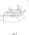
- FIG. 3 illustrates a perspective view of a portion of a phase-change material (PCM) RF switch according to one implementation of the present application
- PCM RF switch 142 is an example of one type of non-volatile RF switch according to the present application.
- PCM RF switch 142 in FIG. 3 may be used as any of non-volatile RF switches 134 a , 134 b , 134 c , 138 a , 138 b , and 138 c in FIG. 2 .
- FIG. 3 illustrates a perspective view of a portion of a phase-change material (PCM) RF switch according to one implementation of the present application
- PCM RF switch 142 in FIG. 3 may be used as any of non-volatile RF switches 134 a , 134 b , 134 c , 138 a , 138 b , and 138 c in FIG. 2 .
- FIG. 3 illustrates a perspective view of a portion of
- PCM RF switch 142 includes substrate 144 , lower dielectric 146 , heating element 148 having terminal segments 150 , thermally conductive and electrically insulating material 152 , PCM 154 having active segment 156 and passive segments 158 , PCM contacts 160 , and heater contacts 162 .
- the perspective view in FIG. 3 shows selected structures of PCM RF switch 142 .
- PCM RF switch 142 may include other structures not shown in FIG. 3 .
- Substrate 144 is situated under lower dielectric 146 .
- substrate 144 is an insulator, such as silicon oxide (SiO 2 ).
- substrate 144 is a silicon (Si), silicon-on-insulator (SOI), sapphire, complementary metal-oxide-semiconductor (CMOS), bipolar CMOS (BiCMOS), or group III-V substrate.
- substrate 144 includes a heat spreader or substrate 144 itself performs as a heat spreader.
- Substrate 144 can have additional layers (not shown in FIG. 3 ).
- substrate 144 can comprise a plurality of interconnect metal levels and interlayer dielectric layers.
- Substrate 144 can also comprise a plurality of devices, such as integrated passive devices (not shown in FIG. 3 ).
- Lower dielectric 146 in PCM RF switch 142 is situated above substrate 144 and below thermally conductive and electrically insulating material 152 . As shown in FIG. 3 , lower dielectric 146 is also adjacent to sides of heating element 148 . Lower dielectric 146 extends along the width of PCM RF switch 142 , and is also coplanar with the top of heating element 148 . Because PCM RF switch 142 includes lower dielectric 146 on the sides of heating element 148 , less heat transfers horizontally (i.e., from the sides) and more heat dissipates vertically from heating element 148 toward active segment 156 of PCM 154 .
- lower dielectric 146 can have a relative width and/or a relative thickness greater or less than shown in FIG. 3 .
- Lower dielectric 146 can comprise any material with thermal conductivity lower than that of thermally conductive and electrically insulating material 152 .
- Heating element 148 in PCM RF switch 142 is situated in lower dielectric 146 .
- Heating element 148 also approximately defines active segment 156 of PCM 154 .
- Heating element 148 generates a crystallizing heat pulse or an amorphizing heat pulse for transforming active segment 156 of PCM 154 .
- Heating element 148 can comprise any material capable of Joule heating.
- Heating element 148 can be connected to electrodes of a pulse generator (not shown in FIG. 3 ) that generates voltage or current pulses.
- heating element 148 comprises a material that exhibits minimal or substantially no electromigration, thermal stress migration, and/or agglomeration.
- heating element 148 can comprise tungsten (W), molybdenum (Mo), titanium (Ti), titanium tungsten (TiW), titanium nitride (TiN), tantalum (Ta), tantalum nitride (TaN), nickel chromium (NiCr), or nickel chromium silicon (NiCrSi).
- heating element 148 comprises tungsten lined with titanium and titanium nitride.
- Thermally conductive and electrically insulating material 152 in PCM RF switch 142 is situated on top of heating element 148 and lower dielectric 146 , and under PCM 154 and, in particular, under active segment 156 of PCM 154 .
- Thermally conductive and electrically insulating material 152 ensures efficient heat transfer from heating element 148 toward active segment 156 of PCM 154 , while electrically insulating heating element 148 from PCM contacts 160 , PCM 154 , and other neighboring structures.
- Thermally conductive and electrically insulating material 152 can comprise any material with high thermal conductivity and high electrical resistivity.
- thermally conductive and electrically insulating material 152 can comprise silicon carbide (Si X C Y ), aluminum nitride (Al X N Y ), aluminum oxide (Al X O Y ), beryllium oxide (Be X O Y ), diamond, or diamond-like carbon.
- thermally conductive and electrically insulating material 152 can be a nugget that does not extend along the width of PCM RF switch 142 .
- thermally conductive and electrically insulating material 152 can be a nugget approximately aligned with heating element 148 .
- PCM 154 in PCM RF switch 142 is situated on top of thermally conductive and electrically insulating material 152 .
- PCM RF switch 142 utilizes PCM 154 to transfer input RF signals in an ON state and to block input RF signals in an OFF state.
- PCM 154 includes active segment 156 and passive segments 158 . Active segment 156 of PCM 154 is approximately defined by heating element 148 . Passive segments 158 of PCM 154 extend outward and are transverse to heating element 148 , and are situated approximately under PCM contacts 160 .
- active segment refers to a segment of PCM that transforms between crystalline and amorphous phases, for example, in response to a crystallizing or an amorphizing heat pulse generated by heating element 148
- passive segment refers to a segment of PCM that does not make such transformation and maintains a crystalline phase (i.e., maintains a conductive state).
- active segment 156 of PCM 154 can transform between crystalline and amorphous phases, allowing PCM RF switch 142 to switch between ON and OFF states respectively. Active segment 156 of PCM 154 must be heated and rapidly quenched in order for PCM RF switch 142 to switch states. If active segment 156 of PCM 154 docs not quench rapidly enough, it will not transform, and PCM RF switch 142 will fail to switch slates. How rapidly active segment 156 of PCM 154 must be quenched depends oil the material, volume, and temperature of PCM 154 . In one implementation, the quench time window can be approximately one hundred nanoseconds (100 ns) or greater or less.
- PCM 154 can comprise germanium telluride (Ge X Te Y ), germanium antimony telluride (Ge X Sb Y Te Z ), germanium selenide (Ge X Se Y ), or any oilier chalcogenide.
- the material for PCM 154 can be chosen based upon ON state resistivity, OFF state electric field breakdown voltage, crystallization temperature, melting temperature, or other considerations. It is noted that in FIG. 3 , heating element 148 is transverse to PCM 154 . Heating element 148 is illustrated with dashed lines as seen through various structures of PCM RF switch 142 . Current flowing in heating element 148 flows approximately under active segment 156 of PCM 154 .
- PCM contacts 160 in PCM RF switch 142 are connected to passive segments 158 of PCM 154 .
- heater contacts 162 are connected to terminal segments 150 of heating element 148 .
- PCM contacts 160 provide RF signals to and from PCM 154 .
- Heater contacts 162 provide power to heating element 148 for generating a crystallizing heat pulse or an amorphizing heat pulse.
- PCM contacts 160 and heater contacts 162 can comprise tungsten (W), copper (Cu), or aluminum (Al).
- PCM contacts 160 and heater contacts 162 can extend through various dielectric layers (not shown in FIG. 3 ).
- PCM contacts 160 can extend through a contact uniformity support layer (not shown in FIG. 3 ) situated on top of PCM 154 , as disclosed in U.S. patent application Ser. No. 16/103,490 filed on Aug. 14, 2018, titled “Manufacturing RF Switch Based on Phase-Change Material.” The disclosure and content of the above-identified application are incorporated fully by reference into the present application.
- PCM RF switch 142 Due to its structure, PCM RF switch 142 has very low insertion loss at radio frequencies.
- PCM 154 in the crystalline state has low resistivity, while PCM 154 in the amorphous state has high resistivity.
- the OFF state resistance (R OFF ) of PCM RF switch 142 can range from approximately ten kilo-Ohms to approximately one mega-Ohm (10 k ⁇ 1 M ⁇ ), while the ON state resistance (R ON ) of PCM RF switch 142 can be approximately one Ohm (1 ⁇ ) or less.
- the low insertion of PCM RF switch 142 is particular advantageous for RF filtering.
- An RF filter such as non-volatile tunable RF filter 126 in FIG. 2 , can employ more PCM RF switches 142 in order to tune its frequency response in more combinations, without insertion losses prohibiting proper RF filtering.
- PCM RF switch 142 is advantageously non-volatile. That is, PCM 154 maintains its crystalline (ON state) or amorphous phase (OFF state) even when power is not supplied to heating element 148 .
- PCM RF switch 142 requires less power than conventional switches when remaining in an ON state.
- PCM RF switch 142 is resilient to voltage fluctuations in its programming, making PCM RF switch 142 particularly applicable in antenna tuners and other circuits which might experience large voltage fluctuations.
- FIG. 4 illustrate a flowchart of an exemplary method for timing an RF module having a non-volatile tunable RF Alter according to one implementation of the present application. Structures shown in FIGS. 5 through 7 illustrate the results of performing the method according to the flowchart in FIG. 4 .
- Actions 164 , 166 , 168 , 170 , and 172 shown in the flowchart in FIG. 4 are sufficient to describe one implementation of die present inventive concepts.
- Other implementations of the present inventive concepts may utilize actions different from those shown in the flowchart of FIG. 4 .
- Certain details and features have been left out of the flowchart that are apparent to a person of ordinary skill in the art. For example, an action may consist of one or more sub-actions or may involve specialized equipment or materials, as known in the art. Moreover, some actions are omitted so as not to distract from the illustrated actions.
- FIG. 5 illustrates a portion of an RF module and a corresponding frequency response graph processed in accordance with actions 164 , 166 , and 168 in the flowchart in FIG. 4 according to one implementation of the present application.
- the RF module includes RF input 102 , amplifier 104 having output 106 , non-volatile tunable RF filter 126 , and RF module output 122 .
- Non-volatile tunable RF filter 126 includes fixed capacitors 110 and 120 , adjustable capacitors 128 and 132 , and adjustable inductor 130 .
- Output 122 of the RF module is coupled to antenna 124 .
- the RF module in FIG. 5 is similar to the RF module in FIG. 2 , except dial, in adjustable capacitors 128 and 132 , non-volatile RF switches 134 a , 134 b , 134 c , 138 a , 138 b , and 138 c in FIG. 2 are shown as PCM RF switches 142 a , 142 b , 142 c , 143 a , 143 b , and 143 c in FIG. 5 .
- PCM RF swatches 142 a , 142 b , and 142 c include respective heating elements 148 a , 148 b , and 148 c , respective PCMs 154 a 154 b and 154 c , respective PCM contacts 160 a , 160 b , and 160 c , and respective heater contacts 162 a , 162 b , and 162 c .
- PCM contacts 160 a , 160 b , and 160 c are coupled to output 106 of amplifier 104 and to respective fixed capacitors 136 a , 136 b , and 136 c .
- PCM RF switches 143 a , 143 b , and 143 c are coupled to node 116 and respective fixed capacitors 140 a , 140 b , and 140 c .
- PCM RF switches 142 a , 142 b , 142 c , 143 a , 143 b , and 143 c in FIG. 5 generally correspond to PCM RF switch 142 in FIG. 3 , and may have any implementations or advantages described above.
- PCMs 154 a , 154 b , and 154 c are situated over and are transverse to respective heating elements 148 a , 148 b , and 148 c .
- heater contacts 162 a , 162 b , and 162 c can provide power to respective heating elements 148 a , 148 b , and 148 c for generating crystallizing heat pulses or amorphizing heat pulses for transforming respective active segments of respective PCMs 154 a , 154 b , and 154 c between crystalline and amorphous phases, thereby switching respective PCM RF switches 142 a , 142 b , and 142 c between ON and OFF states.
- heater contacts 162 a , 162 b , and 162 c are not coupled to a power source and are floating.
- PCM RF switches 143 a , 143 b , and 143 c are not coupled to a power source.
- PCM RF switches 142 a , 142 b , and 142 c are in ON states.
- PCMs 154 a , 154 b , and 154 c are in a crystalline phases, have low resistivity, and are able to easily conduct electrical current.
- a signal at output 106 of amplifier 104 propagates across PCM RF switches 142 a , 142 b , and 142 c through respective first PCM contacts 160 a , 160 b , and 160 c , through respective PCMs 154 a , 154 b , and 154 c , and through respective second PCM contacts 160 a , 160 b , and 160 c , to respective fixed capacitors 136 a , 136 b , and 136 c . Accordingly, all three of fixed capacitors 136 a , 136 b , and 136 c are engaged. In a similar fashion, all three of fixed capacitors 140 a , 140 b , and 140 c are engaged.
- the flowchart begins at action 164 with applying a test RF signal to an amplifier of an RF module.
- a test RF signal can be applied to amplifier 104 of the RF module in FIG. 5 , for example, by connecting a signal generator at RF input 102 .
- the test RF signal can be a frequency sweep or a multi-frequency impulse.
- the flowchart in FIG. 4 continues at action 166 with detecting a desired frequency and an undesired frequency being output by the RF module.
- the frequencies being output by the RF module in FIG. 5 can be detected, for example, by connecting a meter to output 122 of the RF module. In another implementation, frequencies being output by the RF module in FIG. 5 can be detected using a receiver antenna in proximity to antenna 124 .
- Actions 164 and 166 can be performed at the factory by an automated test equipment (ATE).
- ATE automated test equipment
- Frequency response graph 174 in FIG. 5 illustrates the results of performing actions 164 and 166 in the flowchart in FIG. 4 on the RF module in FIG. 5 .
- Trace 176 in frequency response graph 174 illustrates the power at output 122 of the RF module, measured in decibel-milliwatts, versus the frequency, in gigahertz, applied at RF input 102 .
- trace 176 has a maximum near approximately five and a half gigahertz (5.5 GHz) and a minimum near approximately ten gigahertz (10 GHz).
- non-volatile tunable RF filter 126 may have been designed to substantially pass desired frequencies between five gigahertz and six gigahertz (5 GHz-6 GHz), and to substantially reject undesired frequencies between ten gigahertz and twelve gigahertz (10 GHz-12 GHz).
- the desired frequencies may correspond to fundamental frequencies in a wireless communication standard, such as WLAN.
- the undesired frequencies may correspond to second harmonic frequencies in the wireless communication standard.
- Non-volatile tunable RF filter 126 may fail to substantially pass the desired frequencies when a power level is below negative fifteen decibel-milliwatts ( ⁇ 15 dBm).
- Region 178 in frequency response graph 174 indicates the corresponding region where non-volatile tunable RF filter 126 may fail to substantially pass the desired frequencies. Since trace 176 is clear of region 178 , it can be determined that non-volatile tunable RF filler 126 successfully substantially passes the desired frequencies.
- Non-volatile tunable RF filter 126 may fail to substantially reject undesired frequencies when a power level is above negative forty-two decibel-milliwatts ( ⁇ 42 dBm).
- Region 180 in frequency response graph 174 indicates the corresponding region where non-volatile tunable RF filter 126 may fail to substantially reject the undesired frequencies. Since trace 176 intersects region 180 , it can be determined that non-volatile tunable RF filter 126 does not substantially reject the undesired frequencies. In various implementations, any other frequencies may be desired or undesired, and any other power levels may be used to determine whether non-volatile tunable RF filter 126 substantially passes or substantially rejects frequencies.
- FIG. 6 illustrates a portion of an RF module processed in accordance with action 170 in the flowchart in FIG. 4 according to one implementation of the present application, hi the present example, because non-volatile tunable RF filter 126 did not substantially reject the undesired frequencies in FIG. 5 , the flowchart in FIG. 4 continues at action 170 with changing a factory setting of an adjustable capacitor in the non-volatile tunable RF filter by factory-setting a state of a non-volatile RF switch.
- pulse generator 182 is coupled to first heater contacts 162 a and 162 b in respective PCM RF switches 142 a and 142 b in adjustable capacitor 128 .
- Second heater contacts 162 a and 162 b can be coupled to ground (not shown in FIG. 6 ).
- Pulse generator 182 generates electrical pulses and provides power to heating elements 148 a and 148 b .
- Heating elements 148 a and 148 b generate amorphizing heat pulses and transform respective active segments 156 a anti 156 b of respective PCMs 154 a and 154 b to amorphous phases that do not easily conduct electrical current. Accordingly.
- PCM RF switches 142 a and 142 b in FIG. 6 are switched to OFF states, and fixed capacitors 136 a and 136 b are disengaged PCM RF switch 142 c is not coupled to pulse generator 182 , and fixed capacitor 136 c remains engaged.
- pulse generator 182 factory-sets the states of PCM RF switches 142 a and 142 b and correspondingly adjusts the factory setting of adjustable capacitor 128 .
- pulse generator 183 is coupled to a first one of heater contacts 163 c in PCM RF switch 143 c in adjustable capacitor 132 .
- a second one of heater contacts 163 c can be coupled to ground (not shown in FIG. 6 ).
- Pulse generator 183 generates electrical pulses and provides power to heating element 149 c .
- Heating element 149 c generates an amorphizing heat pulse and transforms active segment 157 c of PCM 155 c to an amorphous phase that does not easily conduct electrical current. Accordingly, PCM RF switch 143 c in FIG. 6 is switched to an OFF state, and fixed capacitor 140 c is disengaged.
- PCM RF switches 143 a and 143 b are not coupled to pulse generator 183 , and fixed capacitors 140 a and 140 b remain engaged. Unlike in FIG. 5 , where all three of fixed capacitors 140 a , 140 b , and 140 c were engaged in adjustable capacitor 132 , in FIG. 6 , two fixed capacitors 140 a and 140 b are engaged in adjustable capacitor 132 . Thus, pulse generator 183 factory-sets the state of PCM RF switch 143 c and correspondingly adjusts the factory setting of adjustable capacitor 132 .
- pulse generators 182 and 183 may utilize factor probes for selectively applying electrical pulses to heater contacts of the PCM RF switches during wafer level testing or the level testing prior to packaging. Alternatively, pulse generators 182 and 183 may utilize test pins or functional pins to selectively apply electrical pulses to heater contacts of the PCM RF switches during testing of packaged dies. Although pulse generators 182 and 183 are illustrated as voltage generators in FIG. 6 , in one implementation, pulse generators 182 and 183 can be current generators. Although pulse generator 182 is illustrated as being shared by PCM RF switches 142 a and 142 b , in one implementation, pulse generator 182 may comprise multiple pulse generators connected to respective PCM RF switches.
- pulse generator 182 may be a single pulse generator that is coupled to PCM RF switches 142 a and 142 b one at a time (e.g., coupled to PCM RF switch 142 a first, decoupled therefrom, and then coupled to PCM RF switch 142 b ).
- pulse generator 183 a similar alternative implementation can be used for pulse generator 183 .
- FIG. 6 illustrates concurrently setting the states of three PCM RF switches 142 a , 142 b , and 143 c , more or fewer states can be set at a time.
- FIG. 7 illustrates a portion of an RF module and a corresponding frequency response graph processed in accordance with actions 168 and 172 in the flowchart in FIG. 4 according to one implementation of the present application.
- pulse generators 182 and 183 (shown in FIG. 6 ) are no longer coupled to PCM RF switches 142 a 142 b and 143 c.
- trace 186 illustrates the power at output 122 of the RF module, measured in decibel-milliwatts, versus the frequency, in gigahertz, applied at RF input 102 .
- the RF module in FIG. 7 exhibits a different frequency response compared to the RF module in FIG. 5 , because in FIG. 7 PCM RF switches 142 a 142 b and 143 c are in OFF states and the factory settings of adjustable capacitors 128 and 132 have been changed.
- trace 186 has a maximum near approximately five and a half gigahertz (5.5 GHz) and a minimum near approximately eleven gigahertz (11 GHz). Compared to the profile of trace 176 in FIG. 5 , the profile of trace 186 in FIG. 7 around its minimum is shifted to the right.
- frequency response graph 184 can be used to determine whether non-volatile tunable RF Filter 126 in the RF module in FIG. 7 now substantially rejects an undesired frequency and substantially passes a desired frequency. Since trace 186 is clear of region 178 , it can be determined that non-volatile tunable RF filter 126 in FIG. 7 successfully substantially passes the desired frequencies. Since trace 186 no longer intersects and is clear of region 180 , it can be determined that non-volatile tunable RF filter 126 in FIG. 7 also now successfully substantially rejects the undesired frequencies.
- the factory settings of adjustable capacitors 128 and 132 may need to be changed multiple times before non-volatile tunable RF filter 126 successfully substantially rejects the undesired frequencies. In other words, several iterations of actions 168 and 170 in the flowchart in FIG. 4 may be performed. In one implementation, a factory setting of adjustable inductor 130 can be changed instead of or ill addition to adjustable capacitors 128 and 132 , using a method similar to the one illustrated by the flowchart in FIG. 4 .
- the non-volatile tunable RF filter 126 substantially rejects an undesired frequency and substantially passes a desired frequency in FIG. 7 , the RF module has been successfully factory tuned, and the flowchart in FIG. 4 ends at action 172 with keeping the factory setting of the adjustable capacitor and keeping the corresponding factory-set state of the non-volatile RF switch, and optionally continuing fabrication.
- an end-user can be prevented access to PCM RF switches 142 a , 142 b , 142 c , 143 a , 143 b , and 143 c , so as to prevent the end-user from modifying their factory-set states.
- PCM RF switches 142 a , 142 b , 142 c , 143 a , 143 b , and 143 c may be completely sealed off by packaging.
- PCM RF swatches 142 a , 142 b , 142 c , 143 a , 143 b , and 143 c may be partially sealed off by packaging, and a special interface may be needed to couple to or change the factory-set states of PCM RF switches 142 a , 142 b , 142 c , 143 a , 143 b , and 143 c .
- a controller may prevent a pulse generator from coupling to or providing power to PCM RF switches 142 a , 142 b , 142 c , 143 a , 143 b , and 143 c without hardware or software unlock codes.
- an end-user being “prevented access” does not necessarily require access be completely or absolutely prevented. Rather, it simply means the factory-set states of PCM RF switches cannot be modified by the end-user in the ordinary course of use of an RF module, for example, by using a pulse generator to provide power to PCM RF switches 142 a , 142 b , 142 c , 143 a , 143 b , and 143 c .
- “factory-setting” a state of a non-volatile RF switch does not necessarily require an action to be performed at a factory. Rather, factory-setting can be performed anywhere outside the end-user's ordinary course of use of the RF module.
- factory-setting can be performed at a service center for consumer electronic devices, or at a self-service kiosk.
- “factory-setting” does require the setting to be irreversible.
- a significant advantage of using nonvolatile RF switches such as PCMRF switches 142 a , 142 b , 142 c , 143 a , 143 b , and 143 c , is that, in addition to retaining their states in a non-volatile manner during power off, they are multiple-times-programmable.
- FIG. 8 illustrates a portion of an RF module including a non-volatile tunable RF filter employing an adjustable capacitor according to one implementation of the present application.
- the RF module in FIG. 8 is similar to the tunable RF module in FIG. 2 , except that, where non-volatile tunable RF filter 126 in FIG. 2 included adjustable capacitors 128 and 132 , non-volatile tunable RF filter 127 in FIG. 8 includes adjustable capacitors 188 and 189 .
- adjustable capacitors 188 and 189 employ non-volatile RF switches to engage and disengage selectable segments.
- Adjustable capacitor 188 includes terminals 190 coupled to output 106 of amplifier 104 and terminal 192 coupled to node 116 .
- Adjustable capacitor 189 includes terminal 191 coupled to ground and terminal 193 coupled to node 116 .
- FIG. 9 illustrates a portion of an adjustable capacitor employing PCM RF switches according to one implementation of the present application.
- Adjustable capacitor 188 in FIG. 9 generally corresponds to adjustable capacitors 188 and/or 189 in FIG. 8 .
- Adjustable capacitor 188 in FIG. 9 uses multiple segments and PCM RF switches to provide another technique to change the factory setting of an adjustable capacitor.
- Adjustable capacitor 188 in FIG. 9 includes terminals 190 and 192 , segments 194 and 196 , PCM RF switches 142 and 143 , and selectable segments 198 and 199 .
- adjustable capacitor 188 is an interdigitated capacitor. Segments 194 and 196 and selectable segments 198 and 199 are digits of the interdigitated capacitor. Segments 194 are connected to terminal 190 , while segments 196 are connected to terminal 192 . PCM RF switches 142 and 143 couple terminal 190 to selectable segments 198 and 199 respectively.
- Selectable segments 198 and 199 can be engaged and disengaged by respective PCM RF switches 142 and 143 .
- selectable segments 198 and 199 are disengaged, their shapes and capacitance values effectively do not contribute to the overall shape and capacitance value of the interdigitated capacitor. Rather, the shape and capacitance value are governed by segments 194 and 196 .
- selectable segments 198 and 199 are engaged, their shapes and capacitance values are effectively added, and they increase the overall capacitance value of the interdigitated capacitor.
- selectable segment 199 is engaged, as PCM 155 of PCM RF switch 143 is in a crystalline phase, and selectable segment 198 is disengaged as active segment 156 of PCM 154 of PCM RF switch 142 is in an amorphous phase. Engaging both selectable segments 198 and 199 concurrently will increase the overall capacitance value more than engaging one of selectable segments 198 or 199 .
- Adjustable capacitor 188 can be used as adjustable capacitor 188 in non-volatile tunable RF filter 127 in FIG. 8 .
- adjustable capacitor 188 can include more or fewer segments 194 and 196 and/or more or fewer selectable segments 198 and 199 .
- selectable segments 198 and 199 can have different sizes or shapes than shown in FIG. 9 .
- selectable segments 198 and 199 can be asymmetrical and have different sizes or shapes from each other, such that adjustable capacitor 188 can achieve coarser and finer adjustments.
- selectable segments 198 and 199 may be engaged by more than one PCM RF switch.
- adjustable inductor 130 can be implemented using PCM RF switches and selectable spiral segments (not shown in FIG. 8 or 9 ).
- adjustable capacitor 188 may use any non-volatile RF switches known in the art, instead of or in addition to PCM RF switches 142 and 143 .
Landscapes
- Engineering & Computer Science (AREA)
- Computer Networks & Wireless Communication (AREA)
- Signal Processing (AREA)
- Power Engineering (AREA)
- Physics & Mathematics (AREA)
- Electromagnetism (AREA)
- Filters And Equalizers (AREA)
Abstract
Description
Claims (19)
Priority Applications (1)
| Application Number | Priority Date | Filing Date | Title |
|---|---|---|---|
| US16/775,625 US11139792B2 (en) | 2018-08-14 | 2020-01-29 | Method of tuning a radio frequency (RF) module including a non-volatile tunable RF filter |
Applications Claiming Priority (9)
| Application Number | Priority Date | Filing Date | Title |
|---|---|---|---|
| US16/103,490 US10476001B1 (en) | 2018-08-14 | 2018-08-14 | Manufacturing RF switch based on phase-change material |
| US16/103,646 US10475993B1 (en) | 2018-08-14 | 2018-08-14 | PCM RF switch fabrication with subtractively formed heater |
| US16/103,587 US10461253B1 (en) | 2018-08-14 | 2018-08-14 | High reliability RF switch based on phase-change material |
| US16/114,106 US10707125B2 (en) | 2018-08-14 | 2018-08-27 | Fabrication of contacts in an RF switch having a phase-change material (PCM) and a heating element |
| US16/161,960 US10644235B2 (en) | 2018-08-14 | 2018-10-16 | Phase-change material (PCM) radio frequency (RF) switch with reduced parasitic capacitance |
| US16/418,930 US10536124B1 (en) | 2018-08-14 | 2019-05-21 | Power amplifier module using phase-change material (PCM) radio frequency (RF) switches and selectable matching networks |
| US16/418,130 US11159145B2 (en) | 2018-08-14 | 2019-05-21 | Radio frequency (RF) filtering using phase-change material (PCM) RF switches |
| US16/420,043 US11196401B2 (en) | 2018-08-14 | 2019-05-22 | Radio frequency (RF) module using a tunable RF filter with non-volatile RF switches |
| US16/775,625 US11139792B2 (en) | 2018-08-14 | 2020-01-29 | Method of tuning a radio frequency (RF) module including a non-volatile tunable RF filter |
Related Parent Applications (1)
| Application Number | Title | Priority Date | Filing Date |
|---|---|---|---|
| US16/420,043 Division US11196401B2 (en) | 2018-08-14 | 2019-05-22 | Radio frequency (RF) module using a tunable RF filter with non-volatile RF switches |
Publications (2)
| Publication Number | Publication Date |
|---|---|
| US20200169239A1 US20200169239A1 (en) | 2020-05-28 |
| US11139792B2 true US11139792B2 (en) | 2021-10-05 |
Family
ID=69523576
Family Applications (2)
| Application Number | Title | Priority Date | Filing Date |
|---|---|---|---|
| US16/420,043 Active US11196401B2 (en) | 2018-08-14 | 2019-05-22 | Radio frequency (RF) module using a tunable RF filter with non-volatile RF switches |
| US16/775,625 Active US11139792B2 (en) | 2018-08-14 | 2020-01-29 | Method of tuning a radio frequency (RF) module including a non-volatile tunable RF filter |
Family Applications Before (1)
| Application Number | Title | Priority Date | Filing Date |
|---|---|---|---|
| US16/420,043 Active US11196401B2 (en) | 2018-08-14 | 2019-05-22 | Radio frequency (RF) module using a tunable RF filter with non-volatile RF switches |
Country Status (1)
| Country | Link |
|---|---|
| US (2) | US11196401B2 (en) |
Families Citing this family (7)
| Publication number | Priority date | Publication date | Assignee | Title |
|---|---|---|---|---|
| GB2599986B (en) * | 2020-06-30 | 2025-08-20 | Skyworks Solutions Inc | Tunable filter with mutually coupled inductors |
| US12003263B2 (en) | 2020-08-31 | 2024-06-04 | Skyworks Solutions, Inc. | Radio frequency front end with tunable filters |
| US11201602B1 (en) * | 2020-09-17 | 2021-12-14 | Analog Devices, Inc. | Apparatus and methods for tunable filtering |
| US11201600B1 (en) | 2020-10-05 | 2021-12-14 | Analog Devices, Inc. | Apparatus and methods for control and calibration of tunable filters |
| WO2022265845A1 (en) | 2021-06-18 | 2022-12-22 | Psemi Corporation | Phase-change material switches with isolated heating elements |
| US11624762B2 (en) | 2021-06-18 | 2023-04-11 | Psemi Corporation | Phase-change material switches |
| CN114679197B (en) * | 2022-03-02 | 2024-07-26 | 维沃移动通信有限公司 | Radio frequency circuit, capacitance control method thereof and electronic equipment |
Citations (51)
| Publication number | Priority date | Publication date | Assignee | Title |
|---|---|---|---|---|
| US2014181A (en) | 1933-05-04 | 1935-09-10 | Brehmer Geb | Sheet feed device |
| US2105518A (en) | 1935-07-31 | 1938-01-18 | Rca Corp | Selectivity control system |
| US2140770A (en) | 1937-05-19 | 1938-12-20 | Johnson Lab Inc | Electrical coupling device |
| US2325174A (en) | 1940-11-26 | 1943-07-27 | Emi Ltd | Tuned circuits for wireless receivers |
| US2525566A (en) | 1947-03-11 | 1950-10-10 | British Telecomm Res Ltd | Electric band-pass filter |
| US3496499A (en) | 1966-07-15 | 1970-02-17 | Gen Electric | Constant bandwidth capacitively tuned circuits |
| US6448576B1 (en) * | 2001-08-30 | 2002-09-10 | Bae Systems Information And Electronic Systems Integration, Inc. | Programmable chalcogenide fuse within a semiconductor device |
| US6495998B1 (en) | 2000-09-28 | 2002-12-17 | Sunrise Telecom Corp. | Selectable band-pass filtering apparatus and method |
| US6535545B1 (en) | 1999-10-15 | 2003-03-18 | Rf Waves Ltd. | RF modem utilizing saw resonator and correlator and communications transceiver constructed therefrom |
| US6750734B2 (en) | 2002-05-29 | 2004-06-15 | Ukom, Inc. | Methods and apparatus for tuning an LC filter |
| US20050184828A1 (en) | 2004-02-21 | 2005-08-25 | Samsung Electronics Co., Ltd. | Tunable wideband bandpass filter, tunable multi-band wideband bandpass filter using the same, and methods therefore |
| US20050212090A1 (en) * | 2004-03-25 | 2005-09-29 | Ulrich Friedrich | Integrated circuit |
| US20070080389A1 (en) | 2003-09-22 | 2007-04-12 | Koninklijke Philips Electronics N.V. | Dynamic control of capacitance elements in field effect structures |
| US20070099405A1 (en) | 2005-11-03 | 2007-05-03 | Cswitch Corporation | Methods for fabricating multi-terminal phase change devices |
| US20070246766A1 (en) | 2006-04-04 | 2007-10-25 | Jun Liu | Phase change memory elements using self-aligned phase change material layers and methods of making and using same |
| US20080042243A1 (en) | 2006-08-16 | 2008-02-21 | Industrial Technology Research Institute | Phase change memory devices and methods for fabricating the same |
| US20080142777A1 (en) | 2006-12-13 | 2008-06-19 | Samsung Electronics Co., Ltd. | Phase change memory device including resistant material and method of fabricating the same |
| US20080231759A1 (en) * | 2007-03-20 | 2008-09-25 | Nick Cowley | Removing interfering signals in a broadband radio frequency receiver |
| US20080272355A1 (en) | 2007-05-04 | 2008-11-06 | Samsung Electronics Co., Ltd. | Phase change memory device and method for forming the same |
| US20080291718A1 (en) | 2007-05-25 | 2008-11-27 | Jun Liu | Variable resistance memory device with an interfacial adhesion heating layer, systems using the same and methods of forming the same |
| US20090065761A1 (en) | 2007-09-06 | 2009-03-12 | International Business Machine Corporation | Programmable fuse/non-volatile memory structures in beol regions using externally heated phase change material |
| US20100246247A1 (en) | 2007-08-21 | 2010-09-30 | Kim Doo-Gon | Phase-change random access memories, memory devices, memory systems, methods of operating and methods of manufacturing the same |
| US20110002080A1 (en) | 2008-02-28 | 2011-01-06 | Peregrine Semiconductor Corporation | Method and apparatus for use in digitally tuning a capacitor in an integrated circuit device |
| US20110097825A1 (en) | 2009-10-23 | 2011-04-28 | Macronix International Co., Ltd. | Methods For Reducing Recrystallization Time for a Phase Change Material |
| US20120037872A1 (en) | 2010-08-11 | 2012-02-16 | Sony Corporation | Memory device |
| US8614472B1 (en) | 2011-08-19 | 2013-12-24 | Integrated Device Technology, Inc. | Systems and methods for adjusting ultra-small metal-oxide-metal capacitors |
| US20140110657A1 (en) | 2012-10-23 | 2014-04-24 | Micron Technology, Inc. | Memory constructions |
| US20140191181A1 (en) | 2013-01-09 | 2014-07-10 | Hrl Laboratories, Llc | Method to make rf-pcm switches and circuits with phase-change materials |
| US20140327497A1 (en) | 2013-05-03 | 2014-11-06 | Rfaxis, Inc. | Coupled-resonator on-die filters for wifi applications |
| US20150022938A1 (en) | 2012-01-17 | 2015-01-22 | Rohm Co., Ltd. | Chip capacitor and method for manufacturing the same |
| US20150235971A1 (en) * | 2014-02-14 | 2015-08-20 | Peregrine Semiconductor Corporation | Integrated Tunable Filter Architecture |
| US9257647B2 (en) | 2013-03-14 | 2016-02-09 | Northrop Grumman Systems Corporation | Phase change material switch and method of making the same |
| US20160056373A1 (en) | 2014-08-25 | 2016-02-25 | Qualcomm Switch Corp. | Integrated phase change switch |
| US9362882B1 (en) | 2015-01-23 | 2016-06-07 | Tdk Corporation | Apparatus and methods for segmented variable capacitor arrays |
| US9368720B1 (en) | 2014-05-06 | 2016-06-14 | Hrl Laboratories, Llc | Method to make phase-change material RF switches with thermal dielectrics |
| US20160300612A1 (en) | 2013-12-24 | 2016-10-13 | Sasikanth Manipatruni | Hybrid memory and mtj based mram bit-cell and array |
| US20170133998A1 (en) | 2014-09-08 | 2017-05-11 | Murata Manufacturing Co., Ltd. | Composite component and front-end module |
| US20170187347A1 (en) | 2014-04-18 | 2017-06-29 | Northeastern University | Piezoelectric MEMS Resonator with Integrated Phase Change Material Switches |
| US20170207764A1 (en) | 2015-12-28 | 2017-07-20 | Shanghai Jadic Optoelectronics Technology Co., Ltd | Film Bulk Acoustic Resonator and Method of Fabricating Same |
| US20180005786A1 (en) | 2016-07-04 | 2018-01-04 | Commissariat A L'energie Atomique Et Aux Energies Alternatives | Switch including a phase change materials based structure where only one part is activatable |
| US20180019729A1 (en) | 2015-03-30 | 2018-01-18 | Murata Manufacturing Co., Ltd. | High-frequency filter, front-end circuit, and communication device |
| US20180048305A1 (en) | 2016-08-09 | 2018-02-15 | Skyworks Solutions, Inc. | Radio-frequency switch with switchable capacitor |
| US20180138894A1 (en) | 2016-11-16 | 2018-05-17 | Commissariat A L'energie Atomique Et Aux Energies Alternatives | Switch with phase change material |
| US20180266974A1 (en) | 2017-03-20 | 2018-09-20 | The Boeing Company | Method and system for non-destructive testing |
| US20190088721A1 (en) | 2017-09-19 | 2019-03-21 | Commissariat A L'energie Atomique Et Aux Energies Alternatives | Rf/dc decoupling system for rf switches based on phase change material |
| US10269735B1 (en) * | 2018-06-15 | 2019-04-23 | Globalfoundries Inc. | IC structure with adjustable inductance and capacitance and related method |
| US20190165264A1 (en) | 2017-11-30 | 2019-05-30 | Taiwan Semiconductor Manufacturing Co., Ltd. | Pcram structure with selector device |
| US20190296718A1 (en) | 2016-01-05 | 2019-09-26 | Psemi Corporation | Low Loss Reflective Passive Phase Shifter using Time Delay Element with Double Resolution |
| US10461253B1 (en) | 2018-08-14 | 2019-10-29 | Newport Fab, Llc | High reliability RF switch based on phase-change material |
| US10505106B1 (en) | 2018-10-18 | 2019-12-10 | Toyota Motor Engineering & Manufacturing North America, Inc. | Encapsulated PCM switching devices and methods of forming the same |
| US10529922B1 (en) | 2018-08-14 | 2020-01-07 | Newport Fab, Llc | Substrates and heat spreaders for heat management and RF isolation in integrated semiconductor devices having phase-change material (PCM) radio frequency (RF) switches |
Family Cites Families (43)
| Publication number | Priority date | Publication date | Assignee | Title |
|---|---|---|---|---|
| KR100486306B1 (en) | 2003-02-24 | 2005-04-29 | 삼성전자주식회사 | Phase-change memory device having self-heater structure |
| US7943919B2 (en) | 2003-12-10 | 2011-05-17 | International Business Machines Corporation | Integrated circuit with upstanding stylus |
| TW200529414A (en) | 2004-02-06 | 2005-09-01 | Renesas Tech Corp | Storage |
| EP1677371A1 (en) | 2004-12-30 | 2006-07-05 | STMicroelectronics S.r.l. | Dual resistance heater for phase change devices and manufacturing method thereof |
| US8022382B2 (en) | 2005-03-11 | 2011-09-20 | Taiwan Semiconductor Manufacturing Company, Ltd. | Phase change memory devices with reduced programming current |
| US7414883B2 (en) | 2006-04-20 | 2008-08-19 | Intel Corporation | Programming a normally single phase chalcogenide material for use as a memory or FPLA |
| US7652278B2 (en) | 2006-12-19 | 2010-01-26 | International Business Machines Corporation | Programmable via structure and method of fabricating same |
| US8018760B2 (en) | 2006-12-28 | 2011-09-13 | Panasonic Corporation | Resistance variable element and resistance variable memory apparatus |
| US8379438B2 (en) | 2007-03-30 | 2013-02-19 | Nxp B.V. | Electronic device, and method of operating an electronic device |
| EP2156481B1 (en) | 2007-05-31 | 2012-10-31 | Nxp B.V. | An electronic device comprising a convertible structure, and a method of manufacturing an electronic device |
| JP4607252B2 (en) | 2008-02-25 | 2011-01-05 | パナソニック株式会社 | Driving method of variable resistance element and variable resistance memory device using the same |
| US7920414B2 (en) | 2008-06-06 | 2011-04-05 | Ovonyx, Inc. | Asymmetric-threshold three-terminal switching device |
| US7522029B1 (en) | 2008-07-24 | 2009-04-21 | International Business Machines Corporation | Phase change actuator |
| CN102308344B (en) | 2009-02-10 | 2013-10-16 | 株式会社村田制作所 | Electronic component |
| JP4846816B2 (en) | 2009-03-19 | 2011-12-28 | 株式会社東芝 | Resistance change memory |
| US8314983B2 (en) | 2009-11-10 | 2012-11-20 | International Business Machines Corporation | Nonvolatile nano-electromechanical system device |
| US8345472B2 (en) | 2010-12-21 | 2013-01-01 | Intel Corporation | Three-terminal ovonic threshold switch as a current driver in a phase change memory |
| US8962384B2 (en) | 2012-01-20 | 2015-02-24 | Micron Technology, Inc. | Memory cells having heaters with angled sidewalls |
| JP2013232480A (en) | 2012-04-27 | 2013-11-14 | Toshiba Corp | Semiconductor device and method of manufacturing the same |
| US9853053B2 (en) | 2012-09-10 | 2017-12-26 | 3B Technologies, Inc. | Three dimension integrated circuits employing thin film transistors |
| US8916441B2 (en) | 2013-05-14 | 2014-12-23 | Globalfoundries Inc. | FinFET device and methods of fabrication |
| US9831230B2 (en) | 2013-08-13 | 2017-11-28 | Taiwan Semiconductor Manufacturing Company, Ltd. | Standard cell layout, semiconductor device having engineering change order (ECO) cells and method |
| US9112148B2 (en) | 2013-09-30 | 2015-08-18 | Taiwan Semiconductor Manufacturing Co., Ltd. | RRAM cell structure with laterally offset BEVA/TEVA |
| US9318564B2 (en) | 2014-05-19 | 2016-04-19 | Qualcomm Incorporated | High density static random access memory array having advanced metal patterning |
| WO2016028362A2 (en) | 2014-06-06 | 2016-02-25 | The Regents Of The University Of Michigan | Directly heated rf phase change switch |
| KR102150942B1 (en) | 2014-12-01 | 2020-09-03 | 삼성전자주식회사 | Semiconductor device including fin FET |
| CN107112049A (en) | 2014-12-23 | 2017-08-29 | 3B技术公司 | Three-dimensional integrated circuits using thin film transistors |
| US9584092B2 (en) | 2015-04-14 | 2017-02-28 | International Business Machines Corporation | Mechanical resonator with a spring-mass system comprising a phase-change material |
| US10535713B2 (en) | 2015-09-30 | 2020-01-14 | International Business Machines Corporation | Integrated reactive material erasure element with phase change memory |
| US9444430B1 (en) | 2015-10-02 | 2016-09-13 | International Business Machines Corporation | Cavity filtered qubit |
| US9601545B1 (en) | 2015-10-15 | 2017-03-21 | Taiwan Semiconductor Manufacturing Co., Ltd. | Series MIM structures compatible with RRAM process |
| US10050603B2 (en) | 2015-11-04 | 2018-08-14 | Mediatek Inc. | Frequency tunable filter with voltage stressed relaxed switch, and associated apparatus |
| US9640759B1 (en) | 2015-11-25 | 2017-05-02 | International Business Machines Corporation | Amorphous carbon resistive memory element with lateral heat dissipating structure |
| EP3203309A1 (en) | 2016-02-04 | 2017-08-09 | Bodle Technologies Limited | Optical device with thermally switching phase change material |
| TWI726869B (en) | 2016-02-24 | 2021-05-11 | 聯華電子股份有限公司 | Layout structure for sram and manufacturing methods thereof |
| US10700270B2 (en) | 2016-06-21 | 2020-06-30 | Northrop Grumman Systems Corporation | PCM switch and method of making the same |
| US9891112B1 (en) | 2016-10-19 | 2018-02-13 | International Business Machines Corporation | Radiation detector |
| CN108074789B (en) | 2016-11-15 | 2019-10-11 | 北京北方华创微电子装备有限公司 | A microwave transmission device and semiconductor processing equipment |
| US10315912B2 (en) | 2016-12-28 | 2019-06-11 | Knowles Electronics, Llc | Microelectromechanical system microphone |
| CN108630806A (en) | 2017-03-17 | 2018-10-09 | 中芯国际集成电路制造(上海)有限公司 | Phase transition storage and forming method thereof |
| US9917104B1 (en) | 2017-06-19 | 2018-03-13 | Tower Semiconductor Ltd. | Hybrid MOS-PCM CMOS SOI switch |
| US10505110B2 (en) | 2017-08-28 | 2019-12-10 | Taiwan Semiconductor Manufacturing Co., Ltd. | Phase change memory structure to reduce power consumption |
| US11011323B2 (en) | 2017-12-02 | 2021-05-18 | Bellutech Llc | Sensing devices, sensors, and methods for monitoring environmental conditions |
-
2019
- 2019-05-22 US US16/420,043 patent/US11196401B2/en active Active
-
2020
- 2020-01-29 US US16/775,625 patent/US11139792B2/en active Active
Patent Citations (52)
| Publication number | Priority date | Publication date | Assignee | Title |
|---|---|---|---|---|
| US2014181A (en) | 1933-05-04 | 1935-09-10 | Brehmer Geb | Sheet feed device |
| US2105518A (en) | 1935-07-31 | 1938-01-18 | Rca Corp | Selectivity control system |
| US2140770A (en) | 1937-05-19 | 1938-12-20 | Johnson Lab Inc | Electrical coupling device |
| US2325174A (en) | 1940-11-26 | 1943-07-27 | Emi Ltd | Tuned circuits for wireless receivers |
| US2525566A (en) | 1947-03-11 | 1950-10-10 | British Telecomm Res Ltd | Electric band-pass filter |
| US3496499A (en) | 1966-07-15 | 1970-02-17 | Gen Electric | Constant bandwidth capacitively tuned circuits |
| US6535545B1 (en) | 1999-10-15 | 2003-03-18 | Rf Waves Ltd. | RF modem utilizing saw resonator and correlator and communications transceiver constructed therefrom |
| US6495998B1 (en) | 2000-09-28 | 2002-12-17 | Sunrise Telecom Corp. | Selectable band-pass filtering apparatus and method |
| US6448576B1 (en) * | 2001-08-30 | 2002-09-10 | Bae Systems Information And Electronic Systems Integration, Inc. | Programmable chalcogenide fuse within a semiconductor device |
| US6750734B2 (en) | 2002-05-29 | 2004-06-15 | Ukom, Inc. | Methods and apparatus for tuning an LC filter |
| US20070080389A1 (en) | 2003-09-22 | 2007-04-12 | Koninklijke Philips Electronics N.V. | Dynamic control of capacitance elements in field effect structures |
| US20050184828A1 (en) | 2004-02-21 | 2005-08-25 | Samsung Electronics Co., Ltd. | Tunable wideband bandpass filter, tunable multi-band wideband bandpass filter using the same, and methods therefore |
| US20050212090A1 (en) * | 2004-03-25 | 2005-09-29 | Ulrich Friedrich | Integrated circuit |
| US20070099405A1 (en) | 2005-11-03 | 2007-05-03 | Cswitch Corporation | Methods for fabricating multi-terminal phase change devices |
| US20070246766A1 (en) | 2006-04-04 | 2007-10-25 | Jun Liu | Phase change memory elements using self-aligned phase change material layers and methods of making and using same |
| US20080042243A1 (en) | 2006-08-16 | 2008-02-21 | Industrial Technology Research Institute | Phase change memory devices and methods for fabricating the same |
| US20080142777A1 (en) | 2006-12-13 | 2008-06-19 | Samsung Electronics Co., Ltd. | Phase change memory device including resistant material and method of fabricating the same |
| US20080231759A1 (en) * | 2007-03-20 | 2008-09-25 | Nick Cowley | Removing interfering signals in a broadband radio frequency receiver |
| US20080272355A1 (en) | 2007-05-04 | 2008-11-06 | Samsung Electronics Co., Ltd. | Phase change memory device and method for forming the same |
| US20080291718A1 (en) | 2007-05-25 | 2008-11-27 | Jun Liu | Variable resistance memory device with an interfacial adhesion heating layer, systems using the same and methods of forming the same |
| US20100246247A1 (en) | 2007-08-21 | 2010-09-30 | Kim Doo-Gon | Phase-change random access memories, memory devices, memory systems, methods of operating and methods of manufacturing the same |
| US20090065761A1 (en) | 2007-09-06 | 2009-03-12 | International Business Machine Corporation | Programmable fuse/non-volatile memory structures in beol regions using externally heated phase change material |
| US20110002080A1 (en) | 2008-02-28 | 2011-01-06 | Peregrine Semiconductor Corporation | Method and apparatus for use in digitally tuning a capacitor in an integrated circuit device |
| US20110097825A1 (en) | 2009-10-23 | 2011-04-28 | Macronix International Co., Ltd. | Methods For Reducing Recrystallization Time for a Phase Change Material |
| US20120037872A1 (en) | 2010-08-11 | 2012-02-16 | Sony Corporation | Memory device |
| US8614472B1 (en) | 2011-08-19 | 2013-12-24 | Integrated Device Technology, Inc. | Systems and methods for adjusting ultra-small metal-oxide-metal capacitors |
| US20150022938A1 (en) | 2012-01-17 | 2015-01-22 | Rohm Co., Ltd. | Chip capacitor and method for manufacturing the same |
| US20140110657A1 (en) | 2012-10-23 | 2014-04-24 | Micron Technology, Inc. | Memory constructions |
| US20140191181A1 (en) | 2013-01-09 | 2014-07-10 | Hrl Laboratories, Llc | Method to make rf-pcm switches and circuits with phase-change materials |
| US9257647B2 (en) | 2013-03-14 | 2016-02-09 | Northrop Grumman Systems Corporation | Phase change material switch and method of making the same |
| US20140327497A1 (en) | 2013-05-03 | 2014-11-06 | Rfaxis, Inc. | Coupled-resonator on-die filters for wifi applications |
| US20160300612A1 (en) | 2013-12-24 | 2016-10-13 | Sasikanth Manipatruni | Hybrid memory and mtj based mram bit-cell and array |
| US20150235971A1 (en) * | 2014-02-14 | 2015-08-20 | Peregrine Semiconductor Corporation | Integrated Tunable Filter Architecture |
| US20170187347A1 (en) | 2014-04-18 | 2017-06-29 | Northeastern University | Piezoelectric MEMS Resonator with Integrated Phase Change Material Switches |
| US9368720B1 (en) | 2014-05-06 | 2016-06-14 | Hrl Laboratories, Llc | Method to make phase-change material RF switches with thermal dielectrics |
| US20160056373A1 (en) | 2014-08-25 | 2016-02-25 | Qualcomm Switch Corp. | Integrated phase change switch |
| US20170133998A1 (en) | 2014-09-08 | 2017-05-11 | Murata Manufacturing Co., Ltd. | Composite component and front-end module |
| US9362882B1 (en) | 2015-01-23 | 2016-06-07 | Tdk Corporation | Apparatus and methods for segmented variable capacitor arrays |
| US20180019729A1 (en) | 2015-03-30 | 2018-01-18 | Murata Manufacturing Co., Ltd. | High-frequency filter, front-end circuit, and communication device |
| US20170207764A1 (en) | 2015-12-28 | 2017-07-20 | Shanghai Jadic Optoelectronics Technology Co., Ltd | Film Bulk Acoustic Resonator and Method of Fabricating Same |
| US20190296718A1 (en) | 2016-01-05 | 2019-09-26 | Psemi Corporation | Low Loss Reflective Passive Phase Shifter using Time Delay Element with Double Resolution |
| US20180005786A1 (en) | 2016-07-04 | 2018-01-04 | Commissariat A L'energie Atomique Et Aux Energies Alternatives | Switch including a phase change materials based structure where only one part is activatable |
| US20180048305A1 (en) | 2016-08-09 | 2018-02-15 | Skyworks Solutions, Inc. | Radio-frequency switch with switchable capacitor |
| US20180138894A1 (en) | 2016-11-16 | 2018-05-17 | Commissariat A L'energie Atomique Et Aux Energies Alternatives | Switch with phase change material |
| US10164608B2 (en) | 2016-11-16 | 2018-12-25 | Commissariat A L'energie Atomique Et Aux Energies Alternatives | Switch with phase change material |
| US20180266974A1 (en) | 2017-03-20 | 2018-09-20 | The Boeing Company | Method and system for non-destructive testing |
| US20190088721A1 (en) | 2017-09-19 | 2019-03-21 | Commissariat A L'energie Atomique Et Aux Energies Alternatives | Rf/dc decoupling system for rf switches based on phase change material |
| US20190165264A1 (en) | 2017-11-30 | 2019-05-30 | Taiwan Semiconductor Manufacturing Co., Ltd. | Pcram structure with selector device |
| US10269735B1 (en) * | 2018-06-15 | 2019-04-23 | Globalfoundries Inc. | IC structure with adjustable inductance and capacitance and related method |
| US10461253B1 (en) | 2018-08-14 | 2019-10-29 | Newport Fab, Llc | High reliability RF switch based on phase-change material |
| US10529922B1 (en) | 2018-08-14 | 2020-01-07 | Newport Fab, Llc | Substrates and heat spreaders for heat management and RF isolation in integrated semiconductor devices having phase-change material (PCM) radio frequency (RF) switches |
| US10505106B1 (en) | 2018-10-18 | 2019-12-10 | Toyota Motor Engineering & Manufacturing North America, Inc. | Encapsulated PCM switching devices and methods of forming the same |
Non-Patent Citations (7)
Also Published As
| Publication number | Publication date |
|---|---|
| US20200059217A1 (en) | 2020-02-20 |
| US11196401B2 (en) | 2021-12-07 |
| US20200169239A1 (en) | 2020-05-28 |
Similar Documents
| Publication | Publication Date | Title |
|---|---|---|
| US11139792B2 (en) | Method of tuning a radio frequency (RF) module including a non-volatile tunable RF filter | |
| US10756268B2 (en) | High reliability RF switch based on phase-change material | |
| US10164608B2 (en) | Switch with phase change material | |
| US9917104B1 (en) | Hybrid MOS-PCM CMOS SOI switch | |
| US11159145B2 (en) | Radio frequency (RF) filtering using phase-change material (PCM) RF switches | |
| KR102867831B1 (en) | Switch device, method for operating switch device and method for manufacturing switch device | |
| US11057019B2 (en) | Non-volatile adjustable phase shifter using non-volatile radio frequency (RF) switch | |
| US10593404B2 (en) | Array architecture for large scale integration of phase-change material (PCM) radio frequency (RF) switches | |
| Singh et al. | A reconfigurable dual-frequency narrowband CMOS LNA using phase-change RF switches | |
| US12313703B2 (en) | Low-voltage fuse read circuit | |
| US20250048719A1 (en) | Method to integrate dc & rf phase change switches into high-speed sige bicmos | |
| US10978639B2 (en) | Circuits for reducing RF signal interference and for reducing DC power loss in phase-change material (PCM) RF switches | |
| KR20230150209A (en) | Phase change material switch device and related methods | |
| Liu et al. | Scaled dielectric antifuse structure for field-programmable gate array applications | |
| US10916585B2 (en) | Stacked phase-change material (PCM) radio frequency (RF) switches with improved RF power handling | |
| US20200058851A1 (en) | Semiconductor Devices Having Phase-Change Material (PCM) Radio Frequency (RF) Switches and Integrated Passive Devices | |
| US12527235B2 (en) | Phase change material switch device and related methods | |
| US11158794B2 (en) | High-yield tunable radio frequency (RF) filter with auxiliary capacitors and non-volatile RF switches | |
| US11031555B2 (en) | Power handling improvements for phase-change material (PCM) radio frequency (RF) switch circuits | |
| US10833004B2 (en) | Capacitive tuning circuit using RF switches with PCM capacitors and PCM contact capacitors | |
| US20240114809A1 (en) | Radio frequency switch | |
| CN115004367B (en) | Methods for wafer-level conditioning of protection circuits for electronic devices and wafers for facilitating said methods | |
| US20230422643A1 (en) | Radio frequency switch for multi-band filter applications and methods for forming the same | |
| US10536124B1 (en) | Power amplifier module using phase-change material (PCM) radio frequency (RF) switches and selectable matching networks | |
| JP2019523567A (en) | Method for manufacturing a monolithic microwave integrated circuit (MMIC) and a MMIC having a rapid thermal annealing compensation element |
Legal Events
| Date | Code | Title | Description |
|---|---|---|---|
| FEPP | Fee payment procedure |
Free format text: ENTITY STATUS SET TO UNDISCOUNTED (ORIGINAL EVENT CODE: BIG.); ENTITY STATUS OF PATENT OWNER: LARGE ENTITY |
|
| AS | Assignment |
Owner name: NEWPORT FAB, LLC DBA JAZZ SEMICONDUCTOR, CALIFORNIA Free format text: ASSIGNMENT OF ASSIGNORS INTEREST;ASSIGNORS:MASSE, CHRIS;HOWARD, DAVID J.;EL-HINNAWY, NABIL;AND OTHERS;REEL/FRAME:052136/0792 Effective date: 20190517 |
|
| STPP | Information on status: patent application and granting procedure in general |
Free format text: NON FINAL ACTION MAILED |
|
| STPP | Information on status: patent application and granting procedure in general |
Free format text: DOCKETED NEW CASE - READY FOR EXAMINATION |
|
| STPP | Information on status: patent application and granting procedure in general |
Free format text: NON FINAL ACTION MAILED |
|
| STPP | Information on status: patent application and granting procedure in general |
Free format text: RESPONSE TO NON-FINAL OFFICE ACTION ENTERED AND FORWARDED TO EXAMINER |
|
| STPP | Information on status: patent application and granting procedure in general |
Free format text: NOTICE OF ALLOWANCE MAILED -- APPLICATION RECEIVED IN OFFICE OF PUBLICATIONS |
|
| STPP | Information on status: patent application and granting procedure in general |
Free format text: AWAITING TC RESP., ISSUE FEE NOT PAID |
|
| STPP | Information on status: patent application and granting procedure in general |
Free format text: NOTICE OF ALLOWANCE MAILED -- APPLICATION RECEIVED IN OFFICE OF PUBLICATIONS |
|
| STPP | Information on status: patent application and granting procedure in general |
Free format text: PUBLICATIONS -- ISSUE FEE PAYMENT VERIFIED |
|
| STCF | Information on status: patent grant |
Free format text: PATENTED CASE |
|
| MAFP | Maintenance fee payment |
Free format text: PAYMENT OF MAINTENANCE FEE, 4TH YEAR, LARGE ENTITY (ORIGINAL EVENT CODE: M1551); ENTITY STATUS OF PATENT OWNER: LARGE ENTITY Year of fee payment: 4 |