US11139026B2 - Variable reference based sensing scheme - Google Patents
Variable reference based sensing scheme Download PDFInfo
- Publication number
- US11139026B2 US11139026B2 US16/782,321 US202016782321A US11139026B2 US 11139026 B2 US11139026 B2 US 11139026B2 US 202016782321 A US202016782321 A US 202016782321A US 11139026 B2 US11139026 B2 US 11139026B2
- Authority
- US
- United States
- Prior art keywords
- memory
- voltage
- current
- memory cell
- demarcation
- Prior art date
- Legal status (The legal status is an assumption and is not a legal conclusion. Google has not performed a legal analysis and makes no representation as to the accuracy of the status listed.)
- Active, expires
Links
Images


Classifications
-
- G—PHYSICS
- G11—INFORMATION STORAGE
- G11C—STATIC STORES
- G11C13/00—Digital stores characterised by the use of storage elements not covered by groups G11C11/00, G11C23/00, or G11C25/00
- G11C13/0002—Digital stores characterised by the use of storage elements not covered by groups G11C11/00, G11C23/00, or G11C25/00 using resistive RAM [RRAM] elements
- G11C13/0021—Auxiliary circuits
- G11C13/004—Reading or sensing circuits or methods
-
- G—PHYSICS
- G11—INFORMATION STORAGE
- G11C—STATIC STORES
- G11C16/00—Erasable programmable read-only memories
- G11C16/02—Erasable programmable read-only memories electrically programmable
- G11C16/06—Auxiliary circuits, e.g. for writing into memory
- G11C16/26—Sensing or reading circuits; Data output circuits
-
- G—PHYSICS
- G06—COMPUTING OR CALCULATING; COUNTING
- G06F—ELECTRIC DIGITAL DATA PROCESSING
- G06F3/00—Input arrangements for transferring data to be processed into a form capable of being handled by the computer; Output arrangements for transferring data from processing unit to output unit, e.g. interface arrangements
- G06F3/06—Digital input from, or digital output to, record carriers, e.g. RAID, emulated record carriers or networked record carriers
- G06F3/0601—Interfaces specially adapted for storage systems
- G06F3/0602—Interfaces specially adapted for storage systems specifically adapted to achieve a particular effect
- G06F3/0626—Reducing size or complexity of storage systems
-
- G—PHYSICS
- G06—COMPUTING OR CALCULATING; COUNTING
- G06F—ELECTRIC DIGITAL DATA PROCESSING
- G06F3/00—Input arrangements for transferring data to be processed into a form capable of being handled by the computer; Output arrangements for transferring data from processing unit to output unit, e.g. interface arrangements
- G06F3/06—Digital input from, or digital output to, record carriers, e.g. RAID, emulated record carriers or networked record carriers
- G06F3/0601—Interfaces specially adapted for storage systems
- G06F3/0628—Interfaces specially adapted for storage systems making use of a particular technique
- G06F3/0655—Vertical data movement, i.e. input-output transfer; data movement between one or more hosts and one or more storage devices
- G06F3/0659—Command handling arrangements, e.g. command buffers, queues, command scheduling
-
- G—PHYSICS
- G06—COMPUTING OR CALCULATING; COUNTING
- G06F—ELECTRIC DIGITAL DATA PROCESSING
- G06F3/00—Input arrangements for transferring data to be processed into a form capable of being handled by the computer; Output arrangements for transferring data from processing unit to output unit, e.g. interface arrangements
- G06F3/06—Digital input from, or digital output to, record carriers, e.g. RAID, emulated record carriers or networked record carriers
- G06F3/0601—Interfaces specially adapted for storage systems
- G06F3/0668—Interfaces specially adapted for storage systems adopting a particular infrastructure
- G06F3/0671—In-line storage system
- G06F3/0673—Single storage device
- G06F3/0679—Non-volatile semiconductor memory device, e.g. flash memory, one time programmable memory [OTP]
-
- G—PHYSICS
- G11—INFORMATION STORAGE
- G11C—STATIC STORES
- G11C13/00—Digital stores characterised by the use of storage elements not covered by groups G11C11/00, G11C23/00, or G11C25/00
- G11C13/0002—Digital stores characterised by the use of storage elements not covered by groups G11C11/00, G11C23/00, or G11C25/00 using resistive RAM [RRAM] elements
- G11C13/0004—Digital stores characterised by the use of storage elements not covered by groups G11C11/00, G11C23/00, or G11C25/00 using resistive RAM [RRAM] elements comprising amorphous/crystalline phase transition cells
-
- G—PHYSICS
- G11—INFORMATION STORAGE
- G11C—STATIC STORES
- G11C13/00—Digital stores characterised by the use of storage elements not covered by groups G11C11/00, G11C23/00, or G11C25/00
- G11C13/0002—Digital stores characterised by the use of storage elements not covered by groups G11C11/00, G11C23/00, or G11C25/00 using resistive RAM [RRAM] elements
- G11C13/0021—Auxiliary circuits
- G11C13/003—Cell access
-
- G—PHYSICS
- G11—INFORMATION STORAGE
- G11C—STATIC STORES
- G11C13/00—Digital stores characterised by the use of storage elements not covered by groups G11C11/00, G11C23/00, or G11C25/00
- G11C13/0002—Digital stores characterised by the use of storage elements not covered by groups G11C11/00, G11C23/00, or G11C25/00 using resistive RAM [RRAM] elements
- G11C13/0021—Auxiliary circuits
- G11C13/0035—Evaluating degradation, retention or wearout, e.g. by counting writing cycles
-
- G—PHYSICS
- G11—INFORMATION STORAGE
- G11C—STATIC STORES
- G11C16/00—Erasable programmable read-only memories
- G11C16/02—Erasable programmable read-only memories electrically programmable
- G11C16/06—Auxiliary circuits, e.g. for writing into memory
- G11C16/10—Programming or data input circuits
-
- G—PHYSICS
- G11—INFORMATION STORAGE
- G11C—STATIC STORES
- G11C13/00—Digital stores characterised by the use of storage elements not covered by groups G11C11/00, G11C23/00, or G11C25/00
- G11C13/0002—Digital stores characterised by the use of storage elements not covered by groups G11C11/00, G11C23/00, or G11C25/00 using resistive RAM [RRAM] elements
- G11C13/0021—Auxiliary circuits
- G11C13/004—Reading or sensing circuits or methods
- G11C2013/0045—Read using current through the cell
-
- G—PHYSICS
- G11—INFORMATION STORAGE
- G11C—STATIC STORES
- G11C13/00—Digital stores characterised by the use of storage elements not covered by groups G11C11/00, G11C23/00, or G11C25/00
- G11C13/0002—Digital stores characterised by the use of storage elements not covered by groups G11C11/00, G11C23/00, or G11C25/00 using resistive RAM [RRAM] elements
- G11C13/0021—Auxiliary circuits
- G11C13/004—Reading or sensing circuits or methods
- G11C2013/005—Read using potential difference applied between cell electrodes
-
- G—PHYSICS
- G11—INFORMATION STORAGE
- G11C—STATIC STORES
- G11C13/00—Digital stores characterised by the use of storage elements not covered by groups G11C11/00, G11C23/00, or G11C25/00
- G11C13/0002—Digital stores characterised by the use of storage elements not covered by groups G11C11/00, G11C23/00, or G11C25/00 using resistive RAM [RRAM] elements
- G11C13/0021—Auxiliary circuits
- G11C13/004—Reading or sensing circuits or methods
- G11C2013/0054—Read is performed on a reference element, e.g. cell, and the reference sensed value is used to compare the sensed value of the selected cell
-
- G—PHYSICS
- G11—INFORMATION STORAGE
- G11C—STATIC STORES
- G11C2213/00—Indexing scheme relating to G11C13/00 for features not covered by this group
- G11C2213/70—Resistive array aspects
- G11C2213/76—Array using an access device for each cell which being not a transistor and not a diode
-
- G—PHYSICS
- G11—INFORMATION STORAGE
- G11C—STATIC STORES
- G11C2213/00—Indexing scheme relating to G11C13/00 for features not covered by this group
- G11C2213/70—Resistive array aspects
- G11C2213/77—Array wherein the memory element being directly connected to the bit lines and word lines without any access device being used
Definitions
- the descriptions are generally related to memory, and more particularly, to sensing techniques using variable reference currents for nonvolatile memory, such as crosspoint memory.
- Memory resources have innumerable applications in electronic devices and other computing environments. There is demand for memory technologies that can scale smaller than traditional memory devices. However, continued drive to smaller and more energy efficient devices has resulted in scaling issues with traditional memory devices. Three-dimensional memory devices emerged as a solution to the scaling limitations of traditional memory devices.
- FIG. 1A is circuit diagram of an example of a two-terminal crosspoint memory cell for which the variable reference based sensing technique can be implemented.
- FIG. 1B illustrates an example of threshold voltage distributions of a single level cell (SLC) crosspoint memory cell.
- SLC single level cell
- FIG. 1C illustrates an example of cell current distributions for a read operation and sense current reference placement.
- FIG. 1D illustrates examples of fixed reference current schemes.
- FIG. 2 illustrates an example of a VDM dependent current window and corresponding sense reference currents.
- FIG. 3 illustrates a block diagram of an example of memory device logic to perform a variable reference based sensing scheme.
- FIG. 4A illustrates an example of voltages used for a write algorithm.
- FIG. 4B illustrates an example of two different reference currents for read and write operations.
- FIGS. 5A and 5B are block diagrams of examples of memory device logic to perform a variable reference based sensing scheme.
- FIG. 6 is a flow diagram of an example of variable reference based sensing scheme.
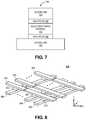
- FIG. 7 illustrates an example of a crosspoint memory cell that can be accessed using techniques described herein.
- FIG. 8 illustrates a portion of a memory cell array.
- FIG. 9 is a block diagram of a system that can include a non-volatile memory device in accordance with examples described herein.
- FIG. 10 provides an exemplary depiction of a computing system.
- Crosspoint memory can be written to and read from by applying particular voltages across crosspoint memory cells.
- One example of a read operation involves applying a voltage across the cell and detecting current through the cell in response to the applied voltage. The magnitude of current through the cell in response to the applied voltage depends on the state of the memory cell. For example, consider a single level (SLC) crosspoint memory cell that can be in one of two states: “set” (e.g., logic 0) or “reset” (e.g., logic 1). If the current through the cell is less than a reference current, the cell is determined to be in a “set” (e.g., logic 0) state. If the current through the cell is greater than the reference current, the cell is determined to be in a “reset” (e.g., logic 1) state.
- set e.g., logic 0
- reset e.g., logic 1
- a static reference current is used to determine the state of the cell.
- the current distributions for set and reset cells can vary based on the magnitude of the applied voltage. Therefore, use of a static reference current for different voltages can reduce or eliminate the “sense window” or separation between the current distributions. Thus, use of a static reference current reduces the flexibility of voltage placement, which in turn increases the bit error rate.
- adjusting the reference current based on the voltage used for sense operations can maximize the sense window and decrease error rate.
- FIG. 1A is circuit diagram of an example of a two-terminal crosspoint memory cell for which the variable reference based sensing technique can be implemented.
- the crosspoint memory cell is one of many memory cells in a crosspoint memory device.
- the crosspoint memory cell 106 is coupled with access circuitry via a bitline 102 and a wordline 104 .
- the crosspoint memory cell 106 includes a material to store one or more bits.
- the memory element of the crosspoint memory cell 106 can include any memory element that can be programmed to two or more stable states.
- the cell 106 can be in one of multiple (e.g., 2, 4 or more) resistive states. In one such example, each different resistive state is associated with a different threshold voltage (VT).
- VT threshold voltage
- a threshold voltage is a voltage at which the cell 106 undergoes a change (e.g., a physical change) that causes the cell to be in a higher conductive state.
- a memory cell can be said to “threshold” or undergo a “threshold event.”
- the memory cell when a memory cell thresholds (e.g., in response to an applied voltage with a magnitude greater than the threshold voltage at the current state), the memory cell undergoes a physical change that causes the memory cell to exhibit certain electrical characteristics, such as high conductivity.
- a program current of a particular amplitude, polarity, and duration can be applied to the cell to cause the cell to be in the desired resistive state.
- the value stored by the crosspoint memory cell 106 can therefore be determined by detecting the resistive state of the cell, which can be determined by detecting the current that flows through the cell in response to an applied voltage.
- the memory cell 106 is coupled with circuitry 108 to enable access to and operation of the memory cell 106 .
- the circuitry includes electronic components that are electrically coupled to perform one or more of: supplying voltages to the memory cell, sensing electrical responses of the memory cell, performing analog or logic operations on received or stored information, outputting information, and storing information.
- the access circuitry 108 includes circuitry to select memory cells, write to memory cells, and read from memory cells.
- FIG. 1B illustrates an example of threshold voltage distributions of a single level cell (SLC) crosspoint memory cell.
- FIG. 1B shows an example of a distribution of threshold voltages for a set cell and for a reset cell.
- a set cell is associated with a “logic 0”
- a reset cell is associated with a “logic 1,” however, the encoding scheme may be different.
- a logic 0 may be associated with a higher magnitude threshold voltage distribution than logic 1.
- a voltage for reading the memory cells is placed between the threshold voltage distributions or set and reset cells.
- the voltage is referred to in the following description as a “demarcation voltage” (VDM); however, the voltage for a sense operation may be referred to as a “read voltage,” “sense voltage,” “reference voltage,” or simply “a voltage.”
- FIG. 1C illustrates an example of cell current distributions for a read operation and sense current reference placement.
- FIG. 1C illustrates two current distributions in response to application of a demarcation voltage for a read operation.
- a demarcation voltage is applied across a reset cell
- a leakage current flows through the memory cell.
- the leakage current is an exponential function of the applied voltage (e.g., the demarcation voltage), among other factors. Therefore, the higher the applied voltage, the higher the leakage current.
- the relationship between leakage current and demarcation voltage can be given by the following equation, where K and a are fitting parameters.
- I leakage K ⁇ e ⁇ (VDM) (Equation 1)
- the leakage current has a distribution with a minimum leakage current I_lkgmin and a maximum leakage current I_lkgmax.
- the leakage current distribution is due to various factors such as temperature, background data patterns, the threshold voltage (Vt) distribution of the cell, and Vt drift of the cell.
- the demarcation voltage applied for performing a sense operation may be adjusted due to threshold voltage movement of the memory cell. For example, a higher or lower magnitude demarcation voltage may be applied due to anticipated threshold voltage drift. If a higher magnitude demarcation voltage is applied, then the magnitude of the leakage current also increases. In the example of FIG. 1C , the maximum leakage current (I_lkgmax) dictates the maximum demarcation voltage.
- both the leakage current and read current are a function of the applied voltage across the memory cell.
- Reset cells conduct a leakage current that is relatively small in magnitude in response to the demarcation voltage.
- Set cells conduct current (“read current”) that is larger in magnitude than the reset cells in response to the demarcation voltage. Therefore, in the example illustrated in FIG. 1C , there is a separation or window 120 between the current distributions for set and reset cells.
- a static reference current (Ireference) is selected to fall between the reset current distribution and the set current distribution. For example, for a sensing operation, the reference current (Ireference) is placed in between the maximum leakage current and the minimum read current.
- the actual current through the cell in response to the demarcation voltage is compared to the selected reference current to determine the state, and thus logic value stored by the cell.
- the sensing is performed by converting the current difference to logic level ‘1’ or ‘0’.
- the logic value stored by the cell can be determined.
- the cell is determined to be in a reset state. If the actual current through the cell is greater than the reference current, the cell is determined to be in a set state.
- This sensing scheme can be performed by comparing the reference current (which is placed in between two current levels) and using an analog current comparator as a sense amplifier to convert the analog signal to logic signal.
- FIG. 1D shows examples of fixed reference current schemes.
- FIG. 1D depicts four current distributions.
- the current distributions 132 and 134 correspond to two different demarcation voltages (VDM 1 and VDM 2 ) applied across reset cells.
- the current distributions 136 and 138 correspond to the two different demarcation voltages applied across set cells.
- VDM 1 and VDM 2 demarcation voltages
- VDM 2 demarcation voltage
- the fixed reference I_REF_FIXED does not move with VDM.
- the window 140 between current distributions begins to shrink as different demarcation voltages are applied.
- the window 140 is defined by the minimum read current in response to VDM 1 and the maximum leakage current in response to VDM 2 .
- the shrinking window may result in bit errors when the fixed reference current fails to fall in the actual window between current distributions.
- FIG. 1D shows an example of a functional failure resulting from the static reference current I_REF_FIXED being placed at a level that overlaps with the leakage current distribution 134 in response to application of VDM 2 .
- the reset cells exhibiting leakage current in the region 142 of the distribution 134 will actually be determined to be set cells in response to VDM 2 .
- the fixed reference current scheme can create functional failure when the leakage current is too high due to a higher VDM for some of the cells, resulting in a higher bit error rate.
- a sense reference current that tracks the demarcation voltage can prevent or minimize shrinkage of the window between current distributions and therefore eliminate restrictions that may lead to suboptimal performance or yield loss.
- FIG. 2 illustrates an example of a VDM dependent current window and corresponding sense reference currents. Like in FIG. 1D , FIG. 2 illustrates current distributions for both reset and set cells in response to two demarcation voltages. However, unlike in FIG. 1D , FIG. 2 shows an example with two different reference currents that correspond to the two demarcation voltages.
- the first reference current I_REF 1 is between the current distributions 202 and 206 for set and reset cells responsive to voltage VDM 1 .
- the second reference current is between current distributions 204 and 208 for set and reset cells responsive to voltage VDM 2 .
- different reference currents are used for read operations based on the demarcation voltages applied to perform the read operations.
- the demarcation voltage is adjusted (e.g., increased) with time to account for effects such as threshold voltage drift.
- a first demarcation voltage VDM 1 is used for read operations.
- a first reference current is used for read operations based on use of the first demarcation voltage.
- a second demarcation voltage VDM 2 is used. Once read operations start using the second demarcation voltage, a second reference current is used for the read operations.
- FIG. 2 shows an example in which the demarcation voltages and reference currents increase in magnitude, the same technique can apply to examples in which the demarcation voltage and reference current decrease in magnitude.
- FIG. 3 illustrates a block diagram of an example of memory device logic to perform a variable reference based sensing scheme.
- the logic 300 is on the memory die.
- the logic 300 may be the same as, similar to, or include the access logic 108 of FIG. 1A .
- the logic 300 receives signals from a controller, such as an ASIC memory controller coupled with the memory die.
- a memory controller sends commands to the memory die to perform operations such as read or write operations.
- the controller provides read VDM information 301 to the logic 300 on the memory die.
- the read VDM information 301 includes a logic value to indicate which reference voltage to use for a read operation (e.g., VDM 1 , VDM 2 , VDM 3 , etc.).
- the control logic 302 receives signals from the controller and performs various control related tasks, such as determining which operation to perform based on the received signals.
- the control logic 302 determines which read reference voltage to use based on the read VDM information 301 and sends a signal to the variable sense reference logic 304 to select the desired reference current.
- the selected demarcation voltage is applied across the memory cell 310 and the selected reference current is provided to sense circuitry (e.g., the sense amplifier 306 ).
- the sense amplifier 306 senses the current through the memory cell 310 and determines what state the memory cell 310 is in by comparing the sensed current with the selected reference current.
- the value stored by the memory cell 310 is then stored in the read sense latch 308 .
- the example in FIG. 3 selects the reference current based on the VDM information supplied by a controller.
- the VDM information may be stored on the die instead of being provided by the controller.
- variable reference based sensing scheme can be used for other sensing operations as well.
- write (or program) operations in some memories involve sensing operations.
- FIG. 4A illustrates an example of voltages used for a write algorithm.
- a first write voltage V_WRITE 1 is applied across a memory cell.
- the first write voltage has a magnitude that is expected to cause most memory cells to threshold (e.g., memory cells having threshold voltages that are lower in magnitude than V_WRITE 1 ), but not all.
- the algorithm involves performing a sensing operation to detect how much current is flowing through the memory cell.
- the memory cell If the memory cell thresholded, it will have “snapped” into a higher conductive state, and therefore will conduct current that is above a threshold. If the memory cell did not threshold, the current through the cell will be less than the threshold. If the memory cell did not threshold, a larger magnitude write voltage is applied to the memory cell (V_WRITE 2 ). Once the memory cell has thresholded, a current can be applied to the cell having a particular magnitude, duration, and polarity to program the memory cell to the desired value.
- One reason to perform a write algorithm involving a lower write voltage followed by a sensing operation is to reduce power consumption by avoiding the higher magnitude voltage in the majority of writes.
- the voltage in order to perform the sensing operation after application of the first write voltage, the voltage is transitioned to a lower magnitude voltage.
- the leakage current is related to the voltage across the cell. Therefore, a high magnitude voltage across the cell may result in a high leakage current. If the voltage across the cell is high enough, it may be difficult or impossible to distinguish between the leakage current and current conducted by a cell that has thresholded.
- the write voltage has a relatively large magnitude, and therefore the voltage is reduced for the sensing operation to a lower demarcation voltage (VDM_THRESHOLD_DET).
- VDM_THRESHOLD_DET demarcation voltage
- the current through the memory cell in response to VDM_THRESHOLD_DET can then be compared to a reference current to determine whether the memory cell thresholded.
- the reference current for the write (threshold or “snapback” detection) sensing operation may be independent and different than the reference current for the read operation.
- FIG. 4B shows an example of two different reference currents for read and write operations.
- the write sensing operation may use a different demarcation voltage than the read sensing operation.
- the current distributions exhibited by memory cells in response to the different demarcation voltages may be different.
- the current distributions 402 and 406 are in response to application of a demarcation voltage applied for a write sensing operation.
- the current distribution 402 represents leakage current through a memory cell that has not thresholded in response to a write voltage.
- the current distribution 406 represents the current through a memory cell that has thresholded in response to a write voltage.
- the current distributions 404 and 408 are in response to application of a demarcation voltage for a read sensing operation for reset and set cells, respectively.
- FIG. 4B illustrates an example in which the reference current I_REF_THRESHOLD_DET is used for threshold detection operations, and a different reference current I_REF_READ is used for read sensing operations.
- the demarcation voltage used for a read operations may change depending on, for example, time.
- the demarcation voltage used for write sensing operations can be static or change. If the write sensing demarcation voltage is static, then a static reference current may suffice for threshold detection sensing operations. However, if the demarcation voltage used for sensing during writes changes, the reference current may be based on the applied demarcation voltage. For example, at an initial time, a first demarcation voltage (VDM_THRESHOLD_DET 1 ) may be used, and then at a later time a second demarcation voltage (VDM_THRESHOLD_DET 2 ) may be used, and so on.
- VDM_THRESHOLD_DET 1 a first demarcation voltage
- VDM_THRESHOLD_DET 2 a second demarcation voltage
- a first reference current (e.g., I_REF_THRESHOLD_DET 1 ) may be used based on the magnitude of VDM_THRESHOLD_DET 1
- a second reference current (e.g., I_REF_THRESHOLD_DET 2 ) may be used based on the magnitude of VDM_THRESHOLD_DET 2
- the variable reference based sensing schemes can be combined; for example, both the reference currents for threshold detection operations and read operations may be selected and based on the applied voltages.
- FIGS. 5A and 5B are block diagrams of examples of memory device logic to perform a variable reference based sensing scheme.
- FIGS. 5A and 5B are similar to FIG. 3 in that they include logic to perform variable reference based sensing, including control logic 302 , variable sense reference logic 304 , a memory cell 310 , a sense amplifier 306 , and latches to store the detected logic values.
- FIG. 5A depicts logic 500 A to enable selection of different reference currents for write threshold detection and read operations.
- the control logic 302 receives a write threshold detection signal 501 from a controller (e.g., an ASIC controller external to the memory die) to indicate that a write command including a sensing operation is to be performed.
- the control logic 302 determines which voltage(s) to apply to perform the write and sensing operations.
- the demarcation voltage used for threshold detection is static (e.g., fused or hard-coded via another mechanism).
- the variable sense reference logic 304 receives a signal indicating the demarcation voltage for the sensing operation and provides the appropriate reference current based on the demarcation voltage to the sense amplifier 306 .
- the selected demarcation voltage is applied across the memory cell 310 and the selected reference current is provided to the sense amplifier 306 .
- the sense amplifier 306 senses the current through the memory cell 310 and determines whether the memory cell thresholded by comparing the sensed current with the selected reference current. The result of the threshold detection operation is then stored in the threshold detection latch 508 .
- FIG. 5B illustrates an example of logic to implement variable reference based sensing for both different read demarcation voltages and for threshold detection.
- the logic 500 B is similar to the logic of FIGS. 3 and 5A .
- the control logic 302 receives both read VDM information 301 to indicate which demarcation is used for the read operation and write threshold detection 501 indicating that the sensing operation is for a write operation.
- the control logic determines the appropriate demarcation voltage to apply across the memory cell 310 based on whether a read or write operation is being performed and may further be based on demarcation voltage information (e.g., information 301 ) provided by the controller.
- the control logic also provides a signal to the sense amplifier indicating whether a read or write operation is being performed. Depending on which operation is being performed, the results of the sensing operation are stored in either the read sense latch 308 or the threshold detection latch 508 .
- the demarcation voltage for the write operation can be varied similarly to the read demarcation voltage.
- the write demarcation voltage may be adjusted (e.g., over time) and the reference current for the write sensing operation can be based on the write demarcation voltage.
- FIGS. 3 and 5B describe a controller external to the memory die providing information indicating the selected read demarcation voltage, in other examples logic internal to the memory die determines the read demarcation voltage.
- FIG. 6 is a flow diagram of an example of variable reference based sensing scheme.
- the method 600 can be performed by hardware, firmware, or a combination of hardware and firmware.
- the method 600 begins with receiving a memory access command to access a crosspoint memory cell, at 602 .
- the memory access command can be, for example, a read command, a write command, or any other command or request to access a memory cell in which a sensing operation is performed.
- Performing the memory access command may involve multiple sub-operations, at least one of which is a sensing operation.
- performance of the sensing operation involves applying a voltage across the memory cell in response to receipt of the memory access command, at 604 .
- the voltage is selected from multiple demarcation voltages.
- the voltage can be a reference or demarcation voltage and may vary depending on whether the memory access command is a read or write command.
- the demarcation voltage may further depend on other factors such as elapsed time (e.g., elapsed time from some initial time).
- control logic selects one of multiple demarcation voltages based on elapsed time.
- the demarcation voltage may be selected based on a signal from a controller, fuses, hard-coded, or from a register setting.
- control logic selects a reference current corresponding to the selected demarcation voltage.
- the selected reference current is one of multiple reference currents, each of which is between expected current distributions at the corresponding demarcation voltage. For example, referring to FIG. 2 , if the memory access command is a read command and the voltage is VDM 1 , a corresponding reference current I_REF 1 is selected. If the memory access command is a read command and the voltage is VDM 2 , a corresponding reference current I_REF 2 is selected. If the memory access command is a write command, a different VDM_THRESHOLD_DET 1 or VDM_THRESHOLD_DET 2 may be selected.
- the current through the cell is then detected, at 608 , and compared to the selected reference current.
- the cell's state can then be determined based on the detected current relative to the selected reference current, at 610 . For example, for a read sensing operation, if the current is above the selected reference current, the memory cell is in one logic state, and if the current is below the selected reference current, the memory cell is in a second logic state. In another example, for a write sensing operation, if the current is below the selected reference current, the memory cell has not thresholded, and if the current is greater than the selected reference current, the memory cell has thresholded.
- the correct state of the memory cells can be determined, reducing bit error rate, which in turn improves yield.
- FIG. 7 illustrates an example of a crosspoint memory cell that can be accessed using techniques described herein.
- FIG. 7 illustrates a memory cell 700 .
- the memory cell 700 includes one or more layers of material 702 to store data and aid in selection of the memory cell 100 .
- the memory cell 700 can include a storage material 702 , a selector material, or both, between access lines 704 and 706 .
- the memory cell includes a layer of storage material and a separate layer of selector material.
- the selector is a device with a threshold voltage and the storage element is a device with a tunable threshold voltage.
- the memory cell 700 includes a self-selecting material that exhibits both memory and selection effects.
- a self-selecting material is a storage material that enables selection of a memory cell in an array without requiring a separate layer of material for selection of the cell.
- a self-selecting memory cell includes a single layer of material that acts as both a selector element to select the memory cell and a memory element to store a logic state.
- a material exhibits memory effects if the material can be put in one of multiple stable states (e.g., via a write operation), and subsequently read back (e.g., via a read operation).
- the storage material is a phase change material. In other examples, the storage material can be in one or multiple stable states without a change in phase.
- the memory element, switching element, or both are amorphous semiconductor threshold switches (e.g., ovonic threshold switches) using an amorphous material such as an amorphous chalcogenide material or other amorphous material.
- An ovonic threshold switch remains in an amorphous state which distinguishes it from an ovonic memory, which generally changes between amorphous and crystalline states.
- an ovonic memory is used in series with an ovonic threshold switch. In such case, the ovonic threshold switch operates as the select device for the ovonic memory.
- the memory could be referred to as a resistance-based memory. In a resistance-based memory, the bit stored by a memory cell is based on the resistive state of the memory cell.
- Examples of storage material can include one or more of: tellurium (Te), selenium (Se), germanium (Ge), antimony (Sb), bismuth (Bi), lead (Pb), tin (Sn), indium (In), silver (Ag), arsenic (As), sulfur (S), phosphorus (P), molybdenum (Mo), gallium (Ga), aluminum (Al), oxygen (O), nitrogen (N), chromium (Cr), gold (Au), niobium (Nb), palladium (Pd), cobalt (Co), vanadium (V), nickel (Ni), platinum (Pt), titanium (Ti), tungsten (W), tantalum (Ta) or other materials.
- the storage material may include one or more chalcogenide materials such as such as Te—Se, Ge—Te, In—Se, Sb—Te, Ge—Sb, Ta—Sb—Te, Ga—Sb, In—Sb, As—Te, As—Se, Al—Te, As—Se—Te, Ge—Sb—Te, Ge—As—Se, Te—Ge—As, V—Sb—Se, Nb—Sb—Se, In—Sb—Te, In—Se—Te, Te—Sn—Se, V—Sb—Te, Se—Te—Sn, Ge—Se—Ga, Mo—Sb—Se, Cr—Sb—Se, Ta—Sb—Se, Bi—Se—Sb, Mo—Sb—Te, Ge—Bi—Te, W—Sb—Se, Ga—Se—Te, Ge—Te—Se, Cr—Sb—Te,
- One or more elements in a chalcogenide material may be dopants.
- the storage material may include dopants such as: aluminum (Al), oxygen (O), nitrogen (N), silicon (Si), carbon (C), boron (B), zirconium (Zr), hafnium (Hf), or a combination thereof.
- the storage material may include other materials or dopants not explicitly listed.
- some memory cells include a separate layer of selector material to form a selector device.
- the selector material may include a chalcogenide material (e.g., a chalcogenide glass) or other material capable of operating as a selection element.
- the selector material includes one or more of: silicon (Si), germanium (Ge), selenium (Se), arsenic, tellurium (Te), or other materials.
- the selector material includes Si—Ge—As—Se, As—Ge—Te—Si, or other selector material.
- the selector material may also include dopants such as: aluminum (Al), oxygen (O), nitrogen (N), silicon (Si), carbon (C), boron (B), zirconium (Zr), hafnium (Hf), or a combination thereof.
- the selector material may include other materials or dopants not explicitly listed.
- the access lines 704 , 706 electrically couple the memory cell with circuitry that provides power to and enables access to the memory cell.
- the term “coupled” can refer to elements that are physically, electrically, and/or communicatively connected either directly or indirectly, and may be used interchangeably with the term “connected” herein. Physical coupling can include direct contact. Electrical coupling includes an interface or interconnection that allows electrical flow and/or signaling between components. Communicative coupling includes connections, including wired and wireless connections, that enable components to exchange data.
- the access lines 704 , 706 can be referred to as a bit line and word line, respectively. The word line is for accessing a particular word in a memory array and the bit line is for accessing a particular bit in the word.
- the access lines 704 , 706 can be composed of one or more metals including: Al, Cu, Ni, Cr, Co, Ru, Rh, Pd, Ag, Pt, Au, Ir, Ta, and W; conductive metal nitrides including TiN, TaN, WN, and TaCN; conductive metal silicides including tantalum silicides, tungsten silicides, nickel silicides, cobalt silicides and titanium silicides; conductive metal silicide nitrides including TiSiN and WSiN; conductive metal carbide nitrides including TiCN and WCN, or any other suitable electrically conductive material.
- metals including: Al, Cu, Ni, Cr, Co, Ru, Rh, Pd, Ag, Pt, Au, Ir, Ta, and W
- conductive metal nitrides including TiN, TaN, WN, and TaCN
- conductive metal silicides including tantalum silicides, tungsten silicides, nickel
- electrodes 708 are disposed between storage material 702 and access lines 704 , 706 . Electrodes 708 electrically couple access lines 704 , 706 with storage material 702 .
- a memory cell with separate layers of storage and selector material may also include an electrode between the layers of storage and selector material.
- Electrodes 708 can be composed of one or more conductive and/or semiconductive materials such as, for example: carbon (C), carbon nitride (C x N y ); n-doped polysilicon and p-doped polysilicon; metals including, Al, Cu, Ni, Cr, Co, Ru, Rh, Pd, Ag, Pt, Au, Ir, Ta, and W; conductive metal nitrides including TiN, TaN, WN, and TaCN; conductive metal silicides including tantalum silicides, tungsten silicides, nickel silicides, cobalt silicides and titanium silicides; conductive metal silicides nitrides including TiSiN and WSiN; conductive metal carbide nitrides including TiCN and WCN; conductive metal oxides including RuO 2 , or other suitable conductive materials.
- C carbon
- C nitride C nitride
- FIG. 8 illustrates a portion of a crosspoint memory array 800 , which can include a memory cell such as the memory cell 106 of FIG. 1 or memory cell 700 of FIG. 7 .
- the memory cell array 800 is an example of a crosspoint memory array.
- the memory cell array 800 includes a plurality of access lines 804 , 806 , which can be the same or similar as the access lines 704 , 706 described with respect to FIG. 7 .
- Access lines 804 , 806 can be referred to as bit lines and word lines.
- the bit lines e.g., access lines 804
- the word lines e.g., access lines 806
- a storage material 802 is disposed between the access lines 804 , 806 .
- a “crosspoint” is formed at an intersection between a bit line, a word line.
- a memory cell is created from the storage material 802 between the bit line and word line where the bit line and word line intersect.
- the storage material 802 can be a chalcogenide material, phase change material, both a chalcogenide material and phase change material, or other storage material.
- the access lines 804 , 806 are composed of one or more conductive materials such as the access lines 704 , 706 described above with respect to FIG. 7 .
- memory cell array 800 typically includes multiple levels or tiers of non-volatile memory cells (e.g., in the z-direction).
- Nonvolatile memory devices including multiple tiers of crosspoint memory cells may be referred to as three-dimensional (3D), multi-level, or multi-tiered crosspoint memory devices.
- 3D three-dimensional
- FIGS. 7 and 8 illustrate an example of a memory cell and array in which the variable reference based sensing techniques described herein may be implemented. However, the techniques described herein can be implemented in memory cell structures and arrays having different materials or structures than the examples described in FIGS. 7 and 8 .
- FIG. 9 is a block diagram of a system that can include a non-volatile memory device in accordance with examples described herein.
- System 900 includes components of a memory subsystem having random access memory (RAM) 920 to store and provide data in response to operations of processor 910 .
- the system 900 receives memory access requests from a host or a processor 910 , which is processing logic that executes operations based on data stored in RAM 920 or generates data to store in RAM 920 .
- the processor 910 can be or include a host processor, central processing unit (CPU), microcontroller or microprocessor, graphics processor, peripheral processor, application specific processor, or other processor, and can be single core or multicore.
- the system 900 includes a memory controller (e.g., host memory controller) 930 , which represents logic to interface with RAM 920 and manage access to data stored in the memory.
- the memory controller 930 is integrated into the hardware of processor 910 .
- the memory controller 930 is standalone hardware, separate from the processor 910 .
- the memory controller 930 can be a separate circuit on a substrate that includes the processor.
- the memory controller 930 can be a separate die or chip integrated on a common substrate with a processor die (e.g., as a system on a chip (SoC)).
- SoC system on a chip
- the memory controller 930 is an integrated memory controller (iMC) integrated as a circuit on the processor die.
- iMC integrated memory controller
- RAM 920 can be included on an SoC with the memory controller 930 and/or the processor 910 .
- the memory controller 930 includes read/write logic 934 , which includes hardware to interface with the RAM 920 .
- the logic 934 enables the memory controller 930 to generate read and write commands to service requests for data access generated by the execution of instructions by processor 910 .
- the memory resources or cachelines in the RAM 920 are represented by a memory cell array 926 , which can include a crosspoint array.
- the RAM 920 includes internal logic 927 to enable control and access of the memory cell array 926 in response to commands received from the controller 922 via an interface 924 (e.g., interface logic).
- the memory array 926 and the controller 922 are in the same package.
- the interface 924 and/or logic 927 can include decode logic, including logic to address specific rows or columns, bit lines or word lines, or otherwise address specific bits of data.
- the controller 922 can be an on-die controller or off-die controller (e.g., ASIC) on the RAM 920 to control its internal operations to execute commands received from memory controller 930 .
- a power source 940 is connected to the RAM 920 to provide one or more voltage rails for operation of the RAM 920 .
- FIG. 10 provides an exemplary depiction of a computing system 1000 (e.g., a smartphone, a tablet computer, a laptop computer, a desktop computer, a server computer, etc.).
- the system 1000 may include one or more processors or processing units 1001 .
- the processor(s) 1001 may include one or more central processing units (CPUs), each of which may include, e.g., a plurality of general-purpose processing cores.
- the processor(s) 1001 may also or alternatively include one or more graphics processing units (GPUs) or other processing units.
- the processor(s) 1001 may include memory management logic (e.g., a memory controller) and I/O control logic.
- the processor(s) 1001 can be similar to, or the same as, the processor 910 of FIG. 9 .
- the system 1000 also includes memory 1002 (e.g., system memory), non-volatile storage 1004 , communications interfaces 1006 , and other components 1008 .
- the other components may include, for example, a display (e.g., touchscreen, flat-panel), a power supply (e.g., a battery or/or other power supply), sensors, power management logic, or other components.
- the communications interfaces 1006 may include logic and/or features to support a communication interface.
- communications interface 1006 may include one or more communication interfaces that operate according to various communication protocols or standards to communicate over direct or network communication links or channels. Direct communications may occur via use of communication protocols or standards described in one or more industry standards (including progenies and variants) such as those associated with the PCIe specification.
- Network communications may occur via use of communication protocols or standards such those described in one or more Ethernet standards promulgated by IEEE.
- one such Ethernet standard may include IEEE 802.3.
- Network communication may also occur according to one or more OpenFlow specifications such as the OpenFlow Switch Specification.
- Other examples of communications interfaces include, for example, a local wired point-to-point link (e.g., USB) interface, a wireless local area network (e.g., WiFi) interface, a wireless point-to-point link (e.g., Bluetooth) interface, a Global Positioning System interface, and/or other interfaces.
- the computing system also includes non-volatile storage 1004 , which may be the mass storage component of the system.
- the non-volatile storage 1004 can be similar to, or the same as, the RAM 920 of FIG. 9 , described above.
- Non-volatile storage 1004 may include byte or block addressable types of non-volatile memory having a crosspoint memory structure.
- Non-volatile types of memory may also include other types of byte or block addressable non-volatile memory such as, but not limited to, multi-threshold level NAND flash memory (e.g., 3D NAND flash memory), NOR flash memory, single or multi-level phase change memory (PCM), resistive memory, nanowire memory, ferroelectric transistor random access memory (FeTRAM), magnetoresistive random access memory (MRAM) that incorporates memristor technology, spin transfer torque MRAM (STT-MRAM), or a combination of any of the above.
- the non-volatile storage 1004 may include mass storage that is composed of one or more SSDs (solid state drives), DIMMs (dual in line memory modules), or other module or drive.
- the non-volatile storage 1004 or memory 1002 may include logic to implement the variable reference based sensing techniques described herein.
- Each component described herein can be a means for performing the operations or functions described.
- Each component described herein includes software, hardware, or a combination of these.
- the components can be implemented as software modules, hardware modules, special-purpose hardware (e.g., application specific hardware, application specific integrated circuits (ASICs), digital signal processors (DSPs), etc.), embedded controllers, hardwired circuitry, etc.
- special-purpose hardware e.g., application specific hardware, application specific integrated circuits (ASICs), digital signal processors (DSPs), etc.
- embedded controllers e.g., hardwired circuitry, etc.
Landscapes
- Engineering & Computer Science (AREA)
- Theoretical Computer Science (AREA)
- Human Computer Interaction (AREA)
- Physics & Mathematics (AREA)
- General Engineering & Computer Science (AREA)
- General Physics & Mathematics (AREA)
- Chemical & Material Sciences (AREA)
- Crystallography & Structural Chemistry (AREA)
- Semiconductor Memories (AREA)
Abstract
Description
I leakage =K×e α(VDM) (Equation 1)
The leakage current has a distribution with a minimum leakage current I_lkgmin and a maximum leakage current I_lkgmax. The leakage current distribution is due to various factors such as temperature, background data patterns, the threshold voltage (Vt) distribution of the cell, and Vt drift of the cell.
I readset =VDM/R path (Equation 2)
In a typical design there is a current mirror in the path to control the current; However, when the actual current flowing through the memory cell is lower than the mirror current due to path resistance, then the current is governed by the equation 2 above rather than the current mirror.
Claims (20)
Priority Applications (3)
| Application Number | Priority Date | Filing Date | Title |
|---|---|---|---|
| US16/782,321 US11139026B2 (en) | 2020-02-05 | 2020-02-05 | Variable reference based sensing scheme |
| DE102020132730.7A DE102020132730A1 (en) | 2020-02-05 | 2020-12-09 | VARIABLE REFERENCE BASED ACQUISITION SCHEME FOR CROSS POINT MEMORY |
| CN202011449147.0A CN113223591A (en) | 2020-02-05 | 2020-12-09 | Variable reference based sensing scheme for cross-point memory |
Applications Claiming Priority (1)
| Application Number | Priority Date | Filing Date | Title |
|---|---|---|---|
| US16/782,321 US11139026B2 (en) | 2020-02-05 | 2020-02-05 | Variable reference based sensing scheme |
Publications (2)
| Publication Number | Publication Date |
|---|---|
| US20210241829A1 US20210241829A1 (en) | 2021-08-05 |
| US11139026B2 true US11139026B2 (en) | 2021-10-05 |
Family
ID=76853694
Family Applications (1)
| Application Number | Title | Priority Date | Filing Date |
|---|---|---|---|
| US16/782,321 Active 2040-04-11 US11139026B2 (en) | 2020-02-05 | 2020-02-05 | Variable reference based sensing scheme |
Country Status (3)
| Country | Link |
|---|---|
| US (1) | US11139026B2 (en) |
| CN (1) | CN113223591A (en) |
| DE (1) | DE102020132730A1 (en) |
Families Citing this family (3)
| Publication number | Priority date | Publication date | Assignee | Title |
|---|---|---|---|---|
| CN113849347B (en) * | 2021-09-27 | 2022-11-11 | 深圳大学 | Data recovery device, method, system and storage medium |
| DE102022104831A1 (en) | 2022-03-01 | 2023-09-07 | TechIFab GmbH | MEMRISTIVE STRUCTURE, MEMRISTIVE CROSSBAR ARRAY AND METHOD THEREOF |
| US12205672B2 (en) | 2022-12-06 | 2025-01-21 | Macronix International Co., Ltd. | Managing reference currents in semiconductor devices |
Citations (5)
| Publication number | Priority date | Publication date | Assignee | Title |
|---|---|---|---|---|
| US20090287975A1 (en) * | 2008-05-15 | 2009-11-19 | Samsung Electronics Co., Ltd. | Memory device and method of managing memory data error |
| US20100124125A1 (en) * | 2008-11-17 | 2010-05-20 | Nec Electronics Corporation | Nonvolatile semiconductor memory device |
| US20140192588A1 (en) * | 2013-01-10 | 2014-07-10 | Samsung Electronics Co., Ltd. | Nonvolatile Memory Device and Read Method Thereof |
| US20150243352A1 (en) * | 2014-02-21 | 2015-08-27 | Samsung Electronics Co., Ltd. | Nonvolatile memory device having resistive memory cell and method sensing data in same |
| US20190088299A1 (en) * | 2017-09-15 | 2019-03-21 | Samsung Electronics Co., Ltd. | Resistive memory device including reference cell and operating method thereof |
-
2020
- 2020-02-05 US US16/782,321 patent/US11139026B2/en active Active
- 2020-12-09 DE DE102020132730.7A patent/DE102020132730A1/en active Pending
- 2020-12-09 CN CN202011449147.0A patent/CN113223591A/en active Pending
Patent Citations (5)
| Publication number | Priority date | Publication date | Assignee | Title |
|---|---|---|---|---|
| US20090287975A1 (en) * | 2008-05-15 | 2009-11-19 | Samsung Electronics Co., Ltd. | Memory device and method of managing memory data error |
| US20100124125A1 (en) * | 2008-11-17 | 2010-05-20 | Nec Electronics Corporation | Nonvolatile semiconductor memory device |
| US20140192588A1 (en) * | 2013-01-10 | 2014-07-10 | Samsung Electronics Co., Ltd. | Nonvolatile Memory Device and Read Method Thereof |
| US20150243352A1 (en) * | 2014-02-21 | 2015-08-27 | Samsung Electronics Co., Ltd. | Nonvolatile memory device having resistive memory cell and method sensing data in same |
| US20190088299A1 (en) * | 2017-09-15 | 2019-03-21 | Samsung Electronics Co., Ltd. | Resistive memory device including reference cell and operating method thereof |
Also Published As
| Publication number | Publication date |
|---|---|
| DE102020132730A1 (en) | 2021-08-05 |
| US20210241829A1 (en) | 2021-08-05 |
| CN113223591A (en) | 2021-08-06 |
Similar Documents
| Publication | Publication Date | Title |
|---|---|---|
| US10777275B2 (en) | Reset refresh techniques for self-selecting memory | |
| US11626161B2 (en) | Selection scheme for crosspoint memory | |
| US11139026B2 (en) | Variable reference based sensing scheme | |
| EP3799050A1 (en) | Techniques to generate & adjust program current pulses for cross-point nonvolatile memory | |
| EP4109454A1 (en) | Cross-point memory read technique to mitigate drift errors | |
| US12361979B2 (en) | Technologies for on-memory die voltage regulator | |
| EP3886103B1 (en) | Multi-level cell (mlc) cross-point memory | |
| US10957387B1 (en) | Multi-level cell (MLC) techniques and circuits for cross-point memory | |
| US11087854B1 (en) | High current fast read scheme for crosspoint memory | |
| US10311948B2 (en) | Phase changeable memory device having a cross point array structure | |
| US9633727B2 (en) | Resistive memory devices and methods of controlling resistive memory devices according to selected pulse power specifications | |
| US12154623B2 (en) | Technologies for controlling current through memory cells | |
| US20230186985A1 (en) | Technologies for dynamic current mirror biasing for memory cells | |
| US20220180934A1 (en) | Read window budget optimization for three dimensional crosspoint memory | |
| US11929117B2 (en) | Phase-change memory devices, systems, and methods of operating thereof | |
| US20230317154A1 (en) | Technologies for dynamic biasing for memory cells | |
| US20230307043A1 (en) | Technologies for current biasing for memory cells | |
| US20260004848A1 (en) | Differential write and read for selector only memory | |
| US20230176747A1 (en) | Memory device with data scrubbing capability and methods | |
| EP4420124A1 (en) | Multi-command memory accesses |
Legal Events
| Date | Code | Title | Description |
|---|---|---|---|
| FEPP | Fee payment procedure |
Free format text: ENTITY STATUS SET TO UNDISCOUNTED (ORIGINAL EVENT CODE: BIG.); ENTITY STATUS OF PATENT OWNER: LARGE ENTITY |
|
| AS | Assignment |
Owner name: INTEL CORPORATION, CALIFORNIA Free format text: ASSIGNMENT OF ASSIGNORS INTEREST;ASSIGNOR:ISLAM, ASHRAF B.;REEL/FRAME:052017/0760 Effective date: 20200207 |
|
| STPP | Information on status: patent application and granting procedure in general |
Free format text: NOTICE OF ALLOWANCE MAILED -- APPLICATION RECEIVED IN OFFICE OF PUBLICATIONS |
|
| STPP | Information on status: patent application and granting procedure in general |
Free format text: PUBLICATIONS -- ISSUE FEE PAYMENT VERIFIED |
|
| STCF | Information on status: patent grant |
Free format text: PATENTED CASE |
|
| MAFP | Maintenance fee payment |
Free format text: PAYMENT OF MAINTENANCE FEE, 4TH YEAR, LARGE ENTITY (ORIGINAL EVENT CODE: M1551); ENTITY STATUS OF PATENT OWNER: LARGE ENTITY Year of fee payment: 4 |