US11131801B2 - Backlight assembly, backlight unit and display panel - Google Patents
Backlight assembly, backlight unit and display panel Download PDFInfo
- Publication number
- US11131801B2 US11131801B2 US16/916,528 US202016916528A US11131801B2 US 11131801 B2 US11131801 B2 US 11131801B2 US 202016916528 A US202016916528 A US 202016916528A US 11131801 B2 US11131801 B2 US 11131801B2
- Authority
- US
- United States
- Prior art keywords
- light source
- heat dissipation
- plate
- back plate
- source plate
- Prior art date
- Legal status (The legal status is an assumption and is not a legal conclusion. Google has not performed a legal analysis and makes no representation as to the accuracy of the status listed.)
- Active
Links
Images


Classifications
-
- G—PHYSICS
- G02—OPTICS
- G02F—OPTICAL DEVICES OR ARRANGEMENTS FOR THE CONTROL OF LIGHT BY MODIFICATION OF THE OPTICAL PROPERTIES OF THE MEDIA OF THE ELEMENTS INVOLVED THEREIN; NON-LINEAR OPTICS; FREQUENCY-CHANGING OF LIGHT; OPTICAL LOGIC ELEMENTS; OPTICAL ANALOGUE/DIGITAL CONVERTERS
- G02F1/00—Devices or arrangements for the control of the intensity, colour, phase, polarisation or direction of light arriving from an independent light source, e.g. switching, gating or modulating; Non-linear optics
- G02F1/01—Devices or arrangements for the control of the intensity, colour, phase, polarisation or direction of light arriving from an independent light source, e.g. switching, gating or modulating; Non-linear optics for the control of the intensity, phase, polarisation or colour
- G02F1/13—Devices or arrangements for the control of the intensity, colour, phase, polarisation or direction of light arriving from an independent light source, e.g. switching, gating or modulating; Non-linear optics for the control of the intensity, phase, polarisation or colour based on liquid crystals, e.g. single liquid crystal display cells
- G02F1/133—Constructional arrangements; Operation of liquid crystal cells; Circuit arrangements
- G02F1/1333—Constructional arrangements; Manufacturing methods
- G02F1/1335—Structural association of cells with optical devices, e.g. polarisers or reflectors
- G02F1/1336—Illuminating devices
- G02F1/133602—Direct backlight
- G02F1/133603—Direct backlight with LEDs
-
- G—PHYSICS
- G02—OPTICS
- G02B—OPTICAL ELEMENTS, SYSTEMS OR APPARATUS
- G02B6/00—Light guides; Structural details of arrangements comprising light guides and other optical elements, e.g. couplings
- G02B6/0001—Light guides; Structural details of arrangements comprising light guides and other optical elements, e.g. couplings specially adapted for lighting devices or systems
- G02B6/0011—Light guides; Structural details of arrangements comprising light guides and other optical elements, e.g. couplings specially adapted for lighting devices or systems the light guides being planar or of plate-like form
- G02B6/0081—Mechanical or electrical aspects of the light guide and light source in the lighting device peculiar to the adaptation to planar light guides, e.g. concerning packaging
- G02B6/0085—Means for removing heat created by the light source from the package
-
- G—PHYSICS
- G02—OPTICS
- G02B—OPTICAL ELEMENTS, SYSTEMS OR APPARATUS
- G02B6/00—Light guides; Structural details of arrangements comprising light guides and other optical elements, e.g. couplings
- G02B6/0001—Light guides; Structural details of arrangements comprising light guides and other optical elements, e.g. couplings specially adapted for lighting devices or systems
- G02B6/0011—Light guides; Structural details of arrangements comprising light guides and other optical elements, e.g. couplings specially adapted for lighting devices or systems the light guides being planar or of plate-like form
- G02B6/0081—Mechanical or electrical aspects of the light guide and light source in the lighting device peculiar to the adaptation to planar light guides, e.g. concerning packaging
- G02B6/0086—Positioning aspects
- G02B6/009—Positioning aspects of the light source in the package
-
- G—PHYSICS
- G02—OPTICS
- G02F—OPTICAL DEVICES OR ARRANGEMENTS FOR THE CONTROL OF LIGHT BY MODIFICATION OF THE OPTICAL PROPERTIES OF THE MEDIA OF THE ELEMENTS INVOLVED THEREIN; NON-LINEAR OPTICS; FREQUENCY-CHANGING OF LIGHT; OPTICAL LOGIC ELEMENTS; OPTICAL ANALOGUE/DIGITAL CONVERTERS
- G02F1/00—Devices or arrangements for the control of the intensity, colour, phase, polarisation or direction of light arriving from an independent light source, e.g. switching, gating or modulating; Non-linear optics
- G02F1/01—Devices or arrangements for the control of the intensity, colour, phase, polarisation or direction of light arriving from an independent light source, e.g. switching, gating or modulating; Non-linear optics for the control of the intensity, phase, polarisation or colour
- G02F1/13—Devices or arrangements for the control of the intensity, colour, phase, polarisation or direction of light arriving from an independent light source, e.g. switching, gating or modulating; Non-linear optics for the control of the intensity, phase, polarisation or colour based on liquid crystals, e.g. single liquid crystal display cells
- G02F1/133—Constructional arrangements; Operation of liquid crystal cells; Circuit arrangements
- G02F1/1333—Constructional arrangements; Manufacturing methods
- G02F1/133308—Support structures for LCD panels, e.g. frames or bezels
-
- G—PHYSICS
- G02—OPTICS
- G02F—OPTICAL DEVICES OR ARRANGEMENTS FOR THE CONTROL OF LIGHT BY MODIFICATION OF THE OPTICAL PROPERTIES OF THE MEDIA OF THE ELEMENTS INVOLVED THEREIN; NON-LINEAR OPTICS; FREQUENCY-CHANGING OF LIGHT; OPTICAL LOGIC ELEMENTS; OPTICAL ANALOGUE/DIGITAL CONVERTERS
- G02F1/00—Devices or arrangements for the control of the intensity, colour, phase, polarisation or direction of light arriving from an independent light source, e.g. switching, gating or modulating; Non-linear optics
- G02F1/01—Devices or arrangements for the control of the intensity, colour, phase, polarisation or direction of light arriving from an independent light source, e.g. switching, gating or modulating; Non-linear optics for the control of the intensity, phase, polarisation or colour
- G02F1/13—Devices or arrangements for the control of the intensity, colour, phase, polarisation or direction of light arriving from an independent light source, e.g. switching, gating or modulating; Non-linear optics for the control of the intensity, phase, polarisation or colour based on liquid crystals, e.g. single liquid crystal display cells
- G02F1/133—Constructional arrangements; Operation of liquid crystal cells; Circuit arrangements
- G02F1/1333—Constructional arrangements; Manufacturing methods
- G02F1/133382—Heating or cooling of liquid crystal cells other than for activation, e.g. circuits or arrangements for temperature control, stabilisation or uniform distribution over the cell
- G02F1/133385—Heating or cooling of liquid crystal cells other than for activation, e.g. circuits or arrangements for temperature control, stabilisation or uniform distribution over the cell with cooling means, e.g. fans
-
- G—PHYSICS
- G02—OPTICS
- G02F—OPTICAL DEVICES OR ARRANGEMENTS FOR THE CONTROL OF LIGHT BY MODIFICATION OF THE OPTICAL PROPERTIES OF THE MEDIA OF THE ELEMENTS INVOLVED THEREIN; NON-LINEAR OPTICS; FREQUENCY-CHANGING OF LIGHT; OPTICAL LOGIC ELEMENTS; OPTICAL ANALOGUE/DIGITAL CONVERTERS
- G02F1/00—Devices or arrangements for the control of the intensity, colour, phase, polarisation or direction of light arriving from an independent light source, e.g. switching, gating or modulating; Non-linear optics
- G02F1/01—Devices or arrangements for the control of the intensity, colour, phase, polarisation or direction of light arriving from an independent light source, e.g. switching, gating or modulating; Non-linear optics for the control of the intensity, phase, polarisation or colour
- G02F1/13—Devices or arrangements for the control of the intensity, colour, phase, polarisation or direction of light arriving from an independent light source, e.g. switching, gating or modulating; Non-linear optics for the control of the intensity, phase, polarisation or colour based on liquid crystals, e.g. single liquid crystal display cells
- G02F1/133—Constructional arrangements; Operation of liquid crystal cells; Circuit arrangements
- G02F1/1333—Constructional arrangements; Manufacturing methods
- G02F1/1335—Structural association of cells with optical devices, e.g. polarisers or reflectors
- G02F1/1336—Illuminating devices
- G02F1/133602—Direct backlight
- G02F1/133608—Direct backlight including particular frames or supporting means
-
- G—PHYSICS
- G02—OPTICS
- G02F—OPTICAL DEVICES OR ARRANGEMENTS FOR THE CONTROL OF LIGHT BY MODIFICATION OF THE OPTICAL PROPERTIES OF THE MEDIA OF THE ELEMENTS INVOLVED THEREIN; NON-LINEAR OPTICS; FREQUENCY-CHANGING OF LIGHT; OPTICAL LOGIC ELEMENTS; OPTICAL ANALOGUE/DIGITAL CONVERTERS
- G02F1/00—Devices or arrangements for the control of the intensity, colour, phase, polarisation or direction of light arriving from an independent light source, e.g. switching, gating or modulating; Non-linear optics
- G02F1/01—Devices or arrangements for the control of the intensity, colour, phase, polarisation or direction of light arriving from an independent light source, e.g. switching, gating or modulating; Non-linear optics for the control of the intensity, phase, polarisation or colour
- G02F1/13—Devices or arrangements for the control of the intensity, colour, phase, polarisation or direction of light arriving from an independent light source, e.g. switching, gating or modulating; Non-linear optics for the control of the intensity, phase, polarisation or colour based on liquid crystals, e.g. single liquid crystal display cells
- G02F1/133—Constructional arrangements; Operation of liquid crystal cells; Circuit arrangements
- G02F1/1333—Constructional arrangements; Manufacturing methods
- G02F1/1335—Structural association of cells with optical devices, e.g. polarisers or reflectors
- G02F1/1336—Illuminating devices
- G02F1/133628—Illuminating devices with cooling means
-
- B—PERFORMING OPERATIONS; TRANSPORTING
- B82—NANOTECHNOLOGY
- B82Y—SPECIFIC USES OR APPLICATIONS OF NANOSTRUCTURES; MEASUREMENT OR ANALYSIS OF NANOSTRUCTURES; MANUFACTURE OR TREATMENT OF NANOSTRUCTURES
- B82Y20/00—Nanooptics, e.g. quantum optics or photonic crystals
-
- G—PHYSICS
- G02—OPTICS
- G02B—OPTICAL ELEMENTS, SYSTEMS OR APPARATUS
- G02B6/00—Light guides; Structural details of arrangements comprising light guides and other optical elements, e.g. couplings
- G02B6/0001—Light guides; Structural details of arrangements comprising light guides and other optical elements, e.g. couplings specially adapted for lighting devices or systems
- G02B6/0011—Light guides; Structural details of arrangements comprising light guides and other optical elements, e.g. couplings specially adapted for lighting devices or systems the light guides being planar or of plate-like form
- G02B6/0033—Means for improving the coupling-out of light from the light guide
- G02B6/005—Means for improving the coupling-out of light from the light guide provided by one optical element, or plurality thereof, placed on the light output side of the light guide
- G02B6/0051—Diffusing sheet or layer
-
- G—PHYSICS
- G02—OPTICS
- G02B—OPTICAL ELEMENTS, SYSTEMS OR APPARATUS
- G02B6/00—Light guides; Structural details of arrangements comprising light guides and other optical elements, e.g. couplings
- G02B6/0001—Light guides; Structural details of arrangements comprising light guides and other optical elements, e.g. couplings specially adapted for lighting devices or systems
- G02B6/0011—Light guides; Structural details of arrangements comprising light guides and other optical elements, e.g. couplings specially adapted for lighting devices or systems the light guides being planar or of plate-like form
- G02B6/0081—Mechanical or electrical aspects of the light guide and light source in the lighting device peculiar to the adaptation to planar light guides, e.g. concerning packaging
- G02B6/0093—Means for protecting the light guide
-
- G—PHYSICS
- G02—OPTICS
- G02F—OPTICAL DEVICES OR ARRANGEMENTS FOR THE CONTROL OF LIGHT BY MODIFICATION OF THE OPTICAL PROPERTIES OF THE MEDIA OF THE ELEMENTS INVOLVED THEREIN; NON-LINEAR OPTICS; FREQUENCY-CHANGING OF LIGHT; OPTICAL LOGIC ELEMENTS; OPTICAL ANALOGUE/DIGITAL CONVERTERS
- G02F1/00—Devices or arrangements for the control of the intensity, colour, phase, polarisation or direction of light arriving from an independent light source, e.g. switching, gating or modulating; Non-linear optics
- G02F1/01—Devices or arrangements for the control of the intensity, colour, phase, polarisation or direction of light arriving from an independent light source, e.g. switching, gating or modulating; Non-linear optics for the control of the intensity, phase, polarisation or colour
- G02F1/13—Devices or arrangements for the control of the intensity, colour, phase, polarisation or direction of light arriving from an independent light source, e.g. switching, gating or modulating; Non-linear optics for the control of the intensity, phase, polarisation or colour based on liquid crystals, e.g. single liquid crystal display cells
- G02F1/133—Constructional arrangements; Operation of liquid crystal cells; Circuit arrangements
- G02F1/1333—Constructional arrangements; Manufacturing methods
- G02F1/133308—Support structures for LCD panels, e.g. frames or bezels
- G02F1/133314—Back frames
-
- G—PHYSICS
- G02—OPTICS
- G02F—OPTICAL DEVICES OR ARRANGEMENTS FOR THE CONTROL OF LIGHT BY MODIFICATION OF THE OPTICAL PROPERTIES OF THE MEDIA OF THE ELEMENTS INVOLVED THEREIN; NON-LINEAR OPTICS; FREQUENCY-CHANGING OF LIGHT; OPTICAL LOGIC ELEMENTS; OPTICAL ANALOGUE/DIGITAL CONVERTERS
- G02F1/00—Devices or arrangements for the control of the intensity, colour, phase, polarisation or direction of light arriving from an independent light source, e.g. switching, gating or modulating; Non-linear optics
- G02F1/01—Devices or arrangements for the control of the intensity, colour, phase, polarisation or direction of light arriving from an independent light source, e.g. switching, gating or modulating; Non-linear optics for the control of the intensity, phase, polarisation or colour
- G02F1/13—Devices or arrangements for the control of the intensity, colour, phase, polarisation or direction of light arriving from an independent light source, e.g. switching, gating or modulating; Non-linear optics for the control of the intensity, phase, polarisation or colour based on liquid crystals, e.g. single liquid crystal display cells
- G02F1/133—Constructional arrangements; Operation of liquid crystal cells; Circuit arrangements
- G02F1/1333—Constructional arrangements; Manufacturing methods
- G02F1/133308—Support structures for LCD panels, e.g. frames or bezels
- G02F1/13332—Front frames
Definitions
- the present disclosure relates to the field of display technology, and particularly relates to a backlight assembly, a backlight unit and a display panel.
- a Mini LED (Mini Light Emitting Diode) (also called sub-millimeter Light Emitting Diode) display is a new display technology in recent years, and has certain advantages over conventional LCD (liquid Crystal display) and OLED (Organic Light-Emitting Diode) display (which may also be referred to as an organic electroluminescent display).
- LCD liquid Crystal display
- OLED Organic Light-Emitting Diode
- a backlight assembly which includes: a back plate and a light source plate, wherein the back plate is provided on a side of the light source plate distal to a light exit side of the light source plate, and the backlight assembly further includes at least one buffer member between the back plate and the light source plate, wherein the backlight assembly further includes at least one heat dissipation member between the back plate and the light source plate, and the at least one heat dissipation member extends from a side of the at least one buffer member proximal to the light source plate to a side of the at least one buffer member proximal to the back plate, and the surfaces, which are in contact with each other, of each of the at least one heat dissipation member, each of the at least one buffer member, the back plate and the light source plate, are fixed to each other.
- the at least one buffer member includes a plurality of buffer members arranged in an array at an equal interval
- the at least one heat dissipation member includes a plurality of heat dissipation members
- at least one buffer member adjacent to each other is taken as a group of buffer members in a row or column direction of the plurality of buffer members, and each of the plurality of heat dissipation members extends from a side of one group of buffer members proximal to the light source plate to a side of an adjacent group of buffer members proximal to the back plate via a space between the one group of buffer members and the adjacent group of buffer members.
- the group of buffer members includes one buffer member.
- the at least one buffer member includes a plurality of buffer members arranged in an array at an equal interval
- the at least one heat dissipation member includes a plurality of heat dissipation members in one-to-one correspondence with the plurality of buffer members
- each of the plurality of heat dissipation members extends from a side of a corresponding buffer member proximal to the light source plate to a side of the corresponding buffer member proximal to the back plate along an edge of the corresponding buffer member.
- orthographic projections of the plurality of heat dissipation members on the light source plate completely cover the light source plate.
- each of the heat dissipation members includes a graphite sheet.
- each of the buffer members includes foam.
- a light source on the light source plate includes a Mini LED.
- surfaces, which are in contact with each other, of two ones of each of the heat dissipation members, each of the buffer members, the back plate and the light source plate, are fixed to each other by an adhesive.
- an adhesive is provided on a surface of each of the buffer members in contact with the light source plate, a surface of each of the buffer members in contact with the back plate, and a surface of each of the buffer members in contact with each of the heat dissipation members; and an adhesive is provided on a surface of each of the heat dissipation members in contact with the light source plate, and a surface of each of the heat dissipation members in contact with the back plate.
- At least one heat dissipation fin is provided on a side of the back plate distal to the light source plate.
- the at least one heat dissipation fin comprises a plurality of heat dissipation fins on a surface of the back plate, the plurality of heat dissipation fins are in parallel with each other and have an equal interval therebetween, and extend in a direction perpendicular to the surface of the back plate.
- the plurality of heat dissipation fins and the back plate are formed as a one-piece structure.
- the back plate has a U-shape
- the light source plate, the at least one buffer member and the at least one heat dissipation member are in a U-shaped space of the back plate.
- a backlight unit which includes the backlight assembly in any one of the embodiments above and a light adjusting layer on a light exit side of the light source plate in the backlight assembly, wherein the light adjusting layer is for adjusting the light emitted from the light source plate.
- the light adjusting layer includes: a light guide plate on the light exit side of the light source plate; a diffuser sheet on a side of the light guide plate distal to the light source plate; a quantum dot film on a side of the diffuser sheet distal to the light guide plate; and a prism on a side of the quantum dot film distal to the diffuser sheet.
- a display panel which includes the backlight unit above and a driving circuit for driving the backlight unit.
- the display panel further includes a display substrate on a light exit side of the backlight unit.
- the display panel further includes a protection frame at both sides of a U-shaped opening of the back plate having a U-shape, to fix the back plate and the display substrate.
- the display panel is a liquid crystal display panel.
- FIG. 1 is a sectional view showing a structure of a liquid crystal display module according to an embodiment of the present disclosure
- FIG. 2 is a sectional view showing a structure of a liquid crystal display module according to an embodiment of the present disclosure
- FIG. 3 is a sectional view showing a structure of a backlight assembly according to an embodiment of the present disclosure
- FIG. 4 is a sectional view showing structures of a buffer member and a heat dissipation member according to an embodiment of the present disclosure
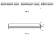
- FIG. 5 is a sectional view showing a structure of a backlight assembly according to an embodiment of the present disclosure
- FIG. 6 is a sectional view showing a structure of a display panel according to an embodiment of the present disclosure.
- FIG. 7 is a sectional view showing a structure of a backlight assembly according to an embodiment of the present disclosure.
- FIG. 8 is a sectional view showing a structure of a backlight assembly according to an embodiment of the present disclosure.
- FIG. 9 is a sectional view showing a structure of a light adjusting layer according to an embodiment of the present disclosure.
- a method for improving the heat dissipation capability mainly adopts active heat dissipation components such as fans and the like which need power to dissipate heat of the Mini LED.
- active heat dissipation components such as fans and the like which need power to dissipate heat of the Mini LED.
- a Mini LED (sub-millimeter light emitting diode) module according to an embodiment of the present disclosure is shown in FIG. 1 , and the Mini LED module serves as a backlight unit in a liquid crystal display module.
- a liquid crystal panel (i.e., a display substrate) 7 in the liquid crystal display module functions as a general liquid crystal display panel.
- a light adjusting layer 6 includes a light guide plate 61 , a diffuser sheet 62 , a quantum dot film 63 , a prism 64 (as shown in FIG. 9 ), and the like. The light adjusting layer 6 is used to adjust light emitted from the Mini LED lamp plate 8 in the backlight unit below.
- the Mini LED lamp plate 8 When the Mini LED lamp plate 8 displays, the Mini LED lamp plate 8 consumes power and the Mini LED lamp plate 8 become a heat source of the whole display module.
- the Mini LED lamp plate 8 and a back plate 1 of the backlight unit are fixed through a double-sided foam rubber 9 .
- the double-sided foam rubber 9 can also play a role in buffering vibration, and avoids the defects such as fracture of the lamp plate, breakage of a chip due to vibration of the Mini LED lamp plate 8 .
- a protection frame 10 (which may be made of metal, such as iron) is provided outside the back plate 1 .
- the protection frame 10 fixes the back plate 1 and the liquid crystal panel 7 , and provides protection for the back plate 1 and the liquid crystal panel 7 .
- the heat from the Mini LED lamp plate 8 can be conducted to the back plate 1 via the foam rubber 9 at first.
- the current conventional foam rubber 9 has a low coefficient of heat conduction, and thus it may be difficult to dissipate heat effectively through the back plate 1 , probably leading to an over high temperature of the Mini LED module.
- FIG. 2 is a Mini LED module for enhancing heat dissipation according to an embodiment of the present disclosure, in which a layer of graphite sheet 13 is used to replace the double-sided foam rubber in FIG. 1 to fix the Mini LED lamp plate 8 , so as to improve heat dissipation performance.
- the graphite sheet 13 is a rigid material and does not function to absorb vibration.
- the Mini LED lamp plate 8 (especially a glass-based Mini LED lamp plate) is prone to problems such as fracture of a lamp plate, breakage of a chip and the like during a drop vibration test.
- the backlight assembly includes: a back plate 1 and a light source plate 2 .
- the back plate 1 is on a side of the light source plate 2 distal to a light exit side of the light source plate 2 .
- the backlight assembly further includes at least one buffer member (which may also be referred to as a shock absorber) 3 , and the buffer member 3 is provided between the back plate 1 and the light source plate 2 .
- the backlight assembly further includes at least one heat dissipation member 4 between the back plate 1 and the light source plate 2 .
- the heat dissipation member 4 extends from a side of the buffer member 3 proximal to the light source plate 2 to a side of the buffer member 3 proximal to the back plate 1 .
- the surfaces, which are in contact with each other, of two ones of the heat dissipation member 4 , the buffer member 3 , the back plate 1 and the light source plate 2 are fixed to each other.
- both ends of each heat dissipation member 4 may be in contact with the light source plate 2 and the back plate 1 , respectively.
- the back plate 1 is made of a material (e.g., a metal such as copper, aluminum, iron, etc.) capable of dissipating heat well, so that heat inside the backlight assembly is effectively dissipated through the back plate 1 .
- the back plate 1 is U-shaped, and the light source plate 2 , the at least one buffer member 3 and the at least one heat dissipation member 4 are provided in a U-shaped space of the back plate 1 .
- the heat dissipation member 4 is arranged to extend from the side of the buffer member 3 proximal to the light source plate 2 to the side of the buffer member 3 proximal to the back plate 1 , so that the heat generated by the light source plate 2 when the light source plate 2 provides the backlight, can be effectively conducted to the back plate 1 through the heat dissipation member 4 , so as to avoid using an active heat dissipation member such as a fan to dissipate heat from the light source plate 2 , thereby reducing power consumption of the backlight assembly and saving consumables of the backlight assembly. At the same time, the heat dissipation capacity of the backlight assembly is further improved.
- the arrangement of the buffer member 3 can buffer the vibration, so that the backlight assembly will not break after being subject to vibration.
- the at least one buffer member 3 may include a plurality of buffer members 3 arranged in an array at an equal interval.
- the at least one heat dissipation member 4 includes a plurality of heat dissipation members. At least one buffer member 3 adjacent to each other is taken as a group of buffer members 3 in a row or column direction of the plurality of buffer members 3 , and each of the heat dissipation members 4 extends from a side of one group of buffer members 3 proximal to the light source plate to a side of an adjacent group (i.e., a group adjacent to the one group) of buffer members 3 proximal to the back plate 1 via a space between the one group of buffer members and the adjacent group of buffer members.
- each heat dissipation member 4 extends from a side of a preceding buffer member 3 proximal to the light source plate 2 to a side of a succeeding buffer member 3 proximal to the back plate 1 .
- the heat dissipation member 4 can also conduct the heat from the light source plate 2 to the back plate 1 effectively, and the heat is dissipated through the back plate 1 , thereby greatly promoting the heat dissipation of the backlight unit.
- the backlight assembly according to the present embodiment can also reduce heat dissipation power consumption and save cost for heat dissipation.
- each group of buffer members 3 there may be a plurality of buffer members in each group of buffer members 3 , and as shown in FIG. 7 , the number of the buffer members in each group of buffer members may be three.
- the at least one heat dissipation member 4 includes a plurality of heat dissipation members in one-to-one correspondence with the plurality of buffer members 3 .
- Each of the plurality of heat dissipation members 4 extends from a side of a corresponding buffer member 3 proximal to the light source plate 2 to a side of the corresponding buffer member 3 proximal to the back plate 1 along an edge of the corresponding buffer member 3 .
- orthographic projections of all the heat dissipation members 4 on the light source plate 2 completely cover the light source plate 2 .
- a contact area of the heat dissipation members 4 and the light source plate 2 can be increased, thereby better conducting heat from the light source plate 2 to the back plate 1 and then dissipating the heat via the back plate 1 when the light source plate 2 provides the backlight.
- each of the heat dissipation members 4 includes a graphite sheet. A plurality of layers of the graphite sheets can be stacked on top of each other, so that the heat can be better conducted and the heat dissipation efficiency can be improved.
- Each of the buffer members 3 includes foam.
- the light sources on the light source plate 2 include sub-millimeter light emitting diodes (i.e. Mini LEDs).
- each of the heat dissipation members 4 is not limited to a graphite sheet, and other materials having good heat dissipation properties (for example, metals such as copper, aluminum, silver, etc.) can be used as the heat dissipation member.
- Each of the buffer members 3 is not limited to foam.
- the light sources are not limited to sub-millimeter light emitting diodes, and other light sources such as LED light sources, OLED light sources, and ordinary white light source lamps are within the scope of the present disclosure.
- an adhesive is provided on the surfaces of the buffer members 3 in contact with the light source plate 2 , the surfaces of the buffer members 3 in contact with the back plate 1 , and the surfaces of the buffer members 3 in contact with the heat dissipation members 4 (as shown in FIG. 3 ).
- the light source plate 2 , the buffer members 3 , the heat dissipation members 4 , and the back plate 1 may be bonded together by the adhesive 11 .
- the adhesive 11 can firmly fix the components in the backlight assembly together.
- the back plate 1 further includes at least one heat dissipation fin 12 on a side of the back plate 1 distal to the light source plate 2 .
- the heat dissipation fins 12 are made of a same material as the back plate 1 , which is capable of dissipating heat effectively.
- the heat dissipation fins 12 can increase the surface area of the back plate 1 , so that the back plate 1 can better dissipate heat generated when the light source plate 2 provides backlight, and the heat dissipation efficiency of the backlight assembly is improved.
- the at least one heat dissipation fin 12 includes a plurality of heat dissipation fins 12 .
- the plurality of heat dissipation fins 12 are parallel to each other and are on the surface (for example, the lower surface shown in FIG. 5 ) of the back plate 1 .
- the heat dissipation fins 12 extend along a direction perpendicular to the surface of the back plate 1 .
- the heat dissipation fins 12 have a certain height in the direction perpendicular to the back plate 1 , which is beneficial to efficient heat dissipation.
- the heat dissipation fins 12 are integrally formed with the back plate 1 . In this way, the heat dissipation can be further promoted, and the heat dissipation efficiency can be improved.
- the heat dissipation member extends from a side of the buffer member proximal to the light source plate to a side of the buffer member proximal to the back plate, so that the heat generated by the light source plate when the light source plate provides backlight, can be effectively conducted to the back plate through the heat dissipation member, so as to avoid using an active heat dissipation member such as a fan to dissipate heat from the light source plate, thereby reducing power consumption of the backlight assembly and saving consumables of the backlight assembly.
- the heat dissipation capacity of the backlight assembly is further improved.
- the buffer member can buffer a vibration, so that the backlight assembly will not break after being subject to the vibration.
- a backlight unit is further provided.
- the backlight unit includes a light adjusting layer and the above-described backlight assembly.
- the light adjusting layer is on a light exit side of the light source plate of the backlight assembly, and is configured to adjust light emitted from the light source plate.
- the light adjusting layer 6 includes a light guide plate 61 , a diffuser sheet 62 , a quantum dot film 63 , a prism 64 , and the like, which are stacked on one another.
- the light guide plate 61 is on the light exit side of the light source plate.
- the diffuser sheet 62 is on a side of the light guide plate distal to the light source plate 2 .
- the quantum dot film 63 is on a side of the diffuser sheet 62 distal to the light guide plate 61 .
- the prism 64 is on a side of the quantum dot film 63 distal to the diffuser sheet 62 .
- the light adjusting layer 6 may be a conventional film layer and structure, and will not be described in detail here.
- the heat dissipation capability of the backlight unit can be further improved by adopting the above backlight assembly, the power consumption for the heat dissipation of the backlight unit can also be reduced, and consumables for heat dissipation of the backlight unit can be saved.
- the backlight unit when each light source on the light source plate is a Mini LED, an LED or an OLED, the backlight unit can be directly used as a display panel, or the backlight unit can also be used as a backlight unit of a liquid crystal display panel.
- a display panel includes the above backlight unit and a driving circuit 14 for driving the backlight unit.
- the driving circuit 14 may be coupled to the light source plate 2 of the backlight unit.
- the display panel may be a liquid crystal display panel, and the display panel further includes a display substrate 7 on the light exit side of the backlight unit.
- the display substrate 7 is on the light exit side of the light adjusting layer 6 in the backlight unit 5 .
- the light adjusting layer 6 is used for adjusting the backlight, so that the adjusted backlight is used as the backlight for display of the display substrate 7 .
- the display substrate 7 may be a known liquid crystal display substrate.
- the display substrate 7 may be coupled to the driving circuit 14 , and the driving circuit 14 may also be used to drive the display substrate 7 to achieve a normal display function.
- the driving circuit 14 may be a known driving circuit or driver.
- a protection frame 10 is provided outside the back plate 1 .
- the protection frame 10 fixes the back plate 1 and the display substrate 7 to connect them together and protect them.
- the protection frame 10 may be provided on two sides of the U-shaped opening of the U-shaped back plate to fix the back plate 1 and the display substrate 7 .
- the protection frame 10 may be made of iron or the like.
- the heat dissipation capability of the display panel can be further improved by adopting the backlight assembly in any one the embodiments of FIGS. 3 to 5 and FIGS. 7 to 8 , the power consumption for the heat dissipation of the display panel can also be reduced, and consumables for heat dissipation of the display panel can be saved.
- the display panel provided by the present disclosure may be any product or component having a display function, such as an LCD panel, an LCD television, a Mini LED panel, a Mini LED television, an OLED panel, an OLED television, a display, a mobile phone, a navigator, and the like.
Landscapes
- Physics & Mathematics (AREA)
- Nonlinear Science (AREA)
- General Physics & Mathematics (AREA)
- Optics & Photonics (AREA)
- Mathematical Physics (AREA)
- Chemical & Material Sciences (AREA)
- Crystallography & Structural Chemistry (AREA)
- Planar Illumination Modules (AREA)
- Liquid Crystal (AREA)
Abstract
Description
Claims (20)
Applications Claiming Priority (2)
| Application Number | Priority Date | Filing Date | Title |
|---|---|---|---|
| CN201911157763.6 | 2019-11-22 | ||
| CN201911157763.6A CN110824773B (en) | 2019-11-22 | 2019-11-22 | Backlight assembly, backlight module and display panel |
Publications (2)
| Publication Number | Publication Date |
|---|---|
| US20210157046A1 US20210157046A1 (en) | 2021-05-27 |
| US11131801B2 true US11131801B2 (en) | 2021-09-28 |
Family
ID=69558316
Family Applications (1)
| Application Number | Title | Priority Date | Filing Date |
|---|---|---|---|
| US16/916,528 Active US11131801B2 (en) | 2019-11-22 | 2020-06-30 | Backlight assembly, backlight unit and display panel |
Country Status (2)
| Country | Link |
|---|---|
| US (1) | US11131801B2 (en) |
| CN (1) | CN110824773B (en) |
Families Citing this family (4)
| Publication number | Priority date | Publication date | Assignee | Title |
|---|---|---|---|---|
| CN111326066B (en) * | 2020-04-08 | 2022-04-26 | 惠州市华星光电技术有限公司 | Back plate, backlight module and display device |
| CN115421332A (en) * | 2022-09-05 | 2022-12-02 | 中国电子科技集团公司第五十五研究所 | Vibration-resistant and high-low temperature-resistant reinforced display backlight assembly |
| EP4700280A2 (en) * | 2022-11-11 | 2026-02-25 | Nichia Corporation | Vehicle lamp |
| CN117148626B (en) * | 2023-08-31 | 2026-04-14 | 合肥京东方瑞晟科技有限公司 | Backlight module and display device |
Citations (14)
| Publication number | Priority date | Publication date | Assignee | Title |
|---|---|---|---|---|
| US20050185110A1 (en) * | 2004-02-19 | 2005-08-25 | Hsin-Chieh Lai | Display module |
| US20120287672A1 (en) * | 2011-05-13 | 2012-11-15 | Samsung Display Co., Ltd. | Backlight assembly and method of assembling a backlight assembly |
| US20130021780A1 (en) * | 2011-07-22 | 2013-01-24 | Sang Hyeok Jung | Backlight unit and display apparatus using the same |
| US20130155335A1 (en) * | 2010-08-24 | 2013-06-20 | Sharpe Kabushiki Kaisha | Illuminating device, display device, and television receiver |
| US20140036536A1 (en) * | 2012-07-31 | 2014-02-06 | Apple Inc. | Mems shutter control for a display utilizing quantum dots |
| US20140226073A1 (en) * | 2011-10-06 | 2014-08-14 | Sharp Kabushiki Kaisha | Illumination device, display device, and television receiving device |
| US20140320747A1 (en) * | 2011-10-06 | 2014-10-30 | Sharp Kabushiki Kaisha | Illumination device, display device, and television receiving device |
| US20150185407A1 (en) * | 2013-12-20 | 2015-07-02 | Shenzhen China Star Optoelectronics Technology Co., Ltd. | Backlight Module And Heat-Dissipating Device |
| US20150205036A1 (en) * | 2012-08-03 | 2015-07-23 | Sharp Kabushiki Kaisha | Lighting device, display device and television device |
| US20160011364A1 (en) * | 2013-05-15 | 2016-01-14 | Sakai Display Products Corporation | Backlight Device and Display Apparatus |
| US20160131831A1 (en) * | 2013-06-07 | 2016-05-12 | Sharp Kabushiki Kaisha | Illumination device, display device, and tv receiver |
| US20170131463A1 (en) * | 2014-07-17 | 2017-05-11 | Sakai Display Products Corporation | Display Apparatus |
| US20170139102A1 (en) * | 2015-11-13 | 2017-05-18 | Le Holdings(Beijing)Co., Ltd. | Backlight module, and liquid crystal display device |
| US20180284338A1 (en) * | 2017-03-30 | 2018-10-04 | Innolux Corporation | Display device |
Family Cites Families (4)
| Publication number | Priority date | Publication date | Assignee | Title |
|---|---|---|---|---|
| CN103851414B (en) * | 2012-12-04 | 2016-08-03 | 盐城华星光电技术有限公司 | Backlight module |
| CN207992647U (en) * | 2018-03-29 | 2018-10-19 | 京东方科技集团股份有限公司 | Backlight module and display device |
| CN108508655B (en) * | 2018-04-24 | 2024-07-19 | 合肥惠科金扬科技有限公司 | Backlight module and display thereof |
| CN110456561A (en) * | 2019-07-29 | 2019-11-15 | 武汉华星光电技术有限公司 | Backlight module and display module |
-
2019
- 2019-11-22 CN CN201911157763.6A patent/CN110824773B/en active Active
-
2020
- 2020-06-30 US US16/916,528 patent/US11131801B2/en active Active
Patent Citations (14)
| Publication number | Priority date | Publication date | Assignee | Title |
|---|---|---|---|---|
| US20050185110A1 (en) * | 2004-02-19 | 2005-08-25 | Hsin-Chieh Lai | Display module |
| US20130155335A1 (en) * | 2010-08-24 | 2013-06-20 | Sharpe Kabushiki Kaisha | Illuminating device, display device, and television receiver |
| US20120287672A1 (en) * | 2011-05-13 | 2012-11-15 | Samsung Display Co., Ltd. | Backlight assembly and method of assembling a backlight assembly |
| US20130021780A1 (en) * | 2011-07-22 | 2013-01-24 | Sang Hyeok Jung | Backlight unit and display apparatus using the same |
| US20140320747A1 (en) * | 2011-10-06 | 2014-10-30 | Sharp Kabushiki Kaisha | Illumination device, display device, and television receiving device |
| US20140226073A1 (en) * | 2011-10-06 | 2014-08-14 | Sharp Kabushiki Kaisha | Illumination device, display device, and television receiving device |
| US20140036536A1 (en) * | 2012-07-31 | 2014-02-06 | Apple Inc. | Mems shutter control for a display utilizing quantum dots |
| US20150205036A1 (en) * | 2012-08-03 | 2015-07-23 | Sharp Kabushiki Kaisha | Lighting device, display device and television device |
| US20160011364A1 (en) * | 2013-05-15 | 2016-01-14 | Sakai Display Products Corporation | Backlight Device and Display Apparatus |
| US20160131831A1 (en) * | 2013-06-07 | 2016-05-12 | Sharp Kabushiki Kaisha | Illumination device, display device, and tv receiver |
| US20150185407A1 (en) * | 2013-12-20 | 2015-07-02 | Shenzhen China Star Optoelectronics Technology Co., Ltd. | Backlight Module And Heat-Dissipating Device |
| US20170131463A1 (en) * | 2014-07-17 | 2017-05-11 | Sakai Display Products Corporation | Display Apparatus |
| US20170139102A1 (en) * | 2015-11-13 | 2017-05-18 | Le Holdings(Beijing)Co., Ltd. | Backlight module, and liquid crystal display device |
| US20180284338A1 (en) * | 2017-03-30 | 2018-10-04 | Innolux Corporation | Display device |
Also Published As
| Publication number | Publication date |
|---|---|
| CN110824773A (en) | 2020-02-21 |
| US20210157046A1 (en) | 2021-05-27 |
| CN110824773B (en) | 2022-08-30 |
Similar Documents
| Publication | Publication Date | Title |
|---|---|---|
| US11131801B2 (en) | Backlight assembly, backlight unit and display panel | |
| US9039219B2 (en) | Display apparatus | |
| CN101583824B (en) | Backlight structure | |
| US11650635B2 (en) | Image display device | |
| CN101589267A (en) | Backlight device and flat display using it | |
| WO2012001998A1 (en) | Lighting apparatus and image display apparatus provided therewith | |
| CN102954399A (en) | Backlight assembly and display apparatus having the same | |
| US9004721B2 (en) | Light source heat dissipation structure and backlight module | |
| CN102654258B (en) | LED Backlight Module | |
| JP4777469B1 (en) | Illumination device and image display device including the same | |
| US9229155B2 (en) | Side-edge backlight module | |
| KR20130088534A (en) | Display device | |
| CN103697378A (en) | Backlight module and display device | |
| JP2009169204A (en) | Liquid crystal display | |
| KR100997638B1 (en) | Device for connecting a led board and chassis and back light utiling the same | |
| US20070147080A1 (en) | Backlight module with a heat conductive block | |
| JP4698643B2 (en) | Bidirectional heat dissipation LED device | |
| JP2010107810A (en) | Light emitting device and electronic equipment | |
| KR20090119405A (en) | Backlight unit | |
| US7602109B2 (en) | Plasma display device | |
| KR101093177B1 (en) | Bracket-integrated heat dissipation printed circuit board for backlight unit and chassis structure having same | |
| KR20080029332A (en) | Backlight Assembly and Display Device Having Same | |
| US20120294040A1 (en) | Light-emitting diode heat-dissipation structure and backlight module | |
| JP5335058B2 (en) | Display device and television receiver | |
| JP3926304B2 (en) | Liquid crystal display |
Legal Events
| Date | Code | Title | Description |
|---|---|---|---|
| FEPP | Fee payment procedure |
Free format text: ENTITY STATUS SET TO UNDISCOUNTED (ORIGINAL EVENT CODE: BIG.); ENTITY STATUS OF PATENT OWNER: LARGE ENTITY |
|
| AS | Assignment |
Owner name: BOE TECHNOLOGY GROUP CO., LTD., CHINA Free format text: ASSIGNMENT OF ASSIGNORS INTEREST;ASSIGNOR:WANG, SHIPENG;REEL/FRAME:053136/0543 Effective date: 20200218 Owner name: BEIJING BOE OPTOELECTRONICS TECHNOLOGY CO., LTD., CHINA Free format text: ASSIGNMENT OF ASSIGNORS INTEREST;ASSIGNOR:WANG, SHIPENG;REEL/FRAME:053136/0543 Effective date: 20200218 |
|
| STPP | Information on status: patent application and granting procedure in general |
Free format text: NOTICE OF ALLOWANCE MAILED -- APPLICATION RECEIVED IN OFFICE OF PUBLICATIONS |
|
| STPP | Information on status: patent application and granting procedure in general |
Free format text: PUBLICATIONS -- ISSUE FEE PAYMENT VERIFIED |
|
| STCF | Information on status: patent grant |
Free format text: PATENTED CASE |
|
| AS | Assignment |
Owner name: BOE TECHNOLOGY GROUP CO., LTD., CHINA Free format text: ASSIGNMENT OF ASSIGNORS INTEREST;ASSIGNORS:BEIJING BOE OPTOELECTRONICS TECHNOLOGY CO., LTD;BOE TECHNOLOGY GROUP CO., LTD.;SIGNING DATES FROM 20220304 TO 20220307;REEL/FRAME:059242/0428 Owner name: BOE MLED TECHNOLOGY CO., LTD., CHINA Free format text: ASSIGNMENT OF ASSIGNORS INTEREST;ASSIGNORS:BEIJING BOE OPTOELECTRONICS TECHNOLOGY CO., LTD;BOE TECHNOLOGY GROUP CO., LTD.;SIGNING DATES FROM 20220304 TO 20220307;REEL/FRAME:059242/0428 |
|
| MAFP | Maintenance fee payment |
Free format text: PAYMENT OF MAINTENANCE FEE, 4TH YEAR, LARGE ENTITY (ORIGINAL EVENT CODE: M1551); ENTITY STATUS OF PATENT OWNER: LARGE ENTITY Year of fee payment: 4 |