US11088445B2 - Antenna assembly with compact layout traces - Google Patents
Antenna assembly with compact layout traces Download PDFInfo
- Publication number
- US11088445B2 US11088445B2 US16/238,632 US201916238632A US11088445B2 US 11088445 B2 US11088445 B2 US 11088445B2 US 201916238632 A US201916238632 A US 201916238632A US 11088445 B2 US11088445 B2 US 11088445B2
- Authority
- US
- United States
- Prior art keywords
- frequency
- low
- antenna
- frequency antenna
- neutralization line
- Prior art date
- Legal status (The legal status is an assumption and is not a legal conclusion. Google has not performed a legal analysis and makes no representation as to the accuracy of the status listed.)
- Active, expires
Links
- 238000006386 neutralization reaction Methods 0.000 claims abstract description 81
- 238000004804 winding Methods 0.000 claims description 8
- 230000005855 radiation Effects 0.000 description 17
- 238000002955 isolation Methods 0.000 description 11
- 238000012360 testing method Methods 0.000 description 8
- 230000005540 biological transmission Effects 0.000 description 5
- 238000004891 communication Methods 0.000 description 5
- 239000010410 layer Substances 0.000 description 5
- 238000013461 design Methods 0.000 description 4
- 230000000295 complement effect Effects 0.000 description 3
- 238000000429 assembly Methods 0.000 description 2
- 230000000712 assembly Effects 0.000 description 2
- 239000003990 capacitor Substances 0.000 description 1
- 230000000694 effects Effects 0.000 description 1
- 238000002474 experimental method Methods 0.000 description 1
- 238000012986 modification Methods 0.000 description 1
- 230000004048 modification Effects 0.000 description 1
- 238000012545 processing Methods 0.000 description 1
- 238000011160 research Methods 0.000 description 1
- 230000008054 signal transmission Effects 0.000 description 1
- 239000002356 single layer Substances 0.000 description 1
- 238000012876 topography Methods 0.000 description 1
- 230000000007 visual effect Effects 0.000 description 1
Images


Classifications
-
- H—ELECTRICITY
- H01—ELECTRIC ELEMENTS
- H01Q—ANTENNAS, i.e. RADIO AERIALS
- H01Q1/00—Details of, or arrangements associated with, antennas
- H01Q1/52—Means for reducing coupling between antennas; Means for reducing coupling between an antenna and another structure
- H01Q1/521—Means for reducing coupling between antennas; Means for reducing coupling between an antenna and another structure reducing the coupling between adjacent antennas
- H01Q1/523—Means for reducing coupling between antennas; Means for reducing coupling between an antenna and another structure reducing the coupling between adjacent antennas between antennas of an array
-
- H—ELECTRICITY
- H01—ELECTRIC ELEMENTS
- H01Q—ANTENNAS, i.e. RADIO AERIALS
- H01Q9/00—Electrically-short antennas having dimensions not more than twice the operating wavelength and consisting of conductive active radiating elements
- H01Q9/04—Resonant antennas
- H01Q9/0407—Substantially flat resonant element parallel to ground plane, e.g. patch antenna
- H01Q9/0421—Substantially flat resonant element parallel to ground plane, e.g. patch antenna with a shorting wall or a shorting pin at one end of the element
-
- H—ELECTRICITY
- H01—ELECTRIC ELEMENTS
- H01Q—ANTENNAS, i.e. RADIO AERIALS
- H01Q1/00—Details of, or arrangements associated with, antennas
- H01Q1/52—Means for reducing coupling between antennas; Means for reducing coupling between an antenna and another structure
- H01Q1/521—Means for reducing coupling between antennas; Means for reducing coupling between an antenna and another structure reducing the coupling between adjacent antennas
-
- H—ELECTRICITY
- H01—ELECTRIC ELEMENTS
- H01Q—ANTENNAS, i.e. RADIO AERIALS
- H01Q21/00—Antenna arrays or systems
- H01Q21/0006—Particular feeding systems
-
- H—ELECTRICITY
- H01—ELECTRIC ELEMENTS
- H01Q—ANTENNAS, i.e. RADIO AERIALS
- H01Q5/00—Arrangements for simultaneous operation of antennas on two or more different wavebands, e.g. dual-band or multi-band arrangements
- H01Q5/30—Arrangements for providing operation on different wavebands
- H01Q5/307—Individual or coupled radiating elements, each element being fed in an unspecified way
-
- H—ELECTRICITY
- H01—ELECTRIC ELEMENTS
- H01Q—ANTENNAS, i.e. RADIO AERIALS
- H01Q5/00—Arrangements for simultaneous operation of antennas on two or more different wavebands, e.g. dual-band or multi-band arrangements
- H01Q5/40—Imbricated or interleaved structures; Combined or electromagnetically coupled arrangements, e.g. comprising two or more non-connected fed radiating elements
- H01Q5/42—Imbricated or interleaved structures; Combined or electromagnetically coupled arrangements, e.g. comprising two or more non-connected fed radiating elements using two or more imbricated arrays
Definitions
- the present invention relates to an antenna assembly and more particularly to one applicable to a MIMO product and with antennas of the same working band arranged along the same edge of a circuit board.
- the IEEE 802.11n standard additionally allows for the multi-input multi-output (MIMO) mode, which incorporates the smart antenna design (to help transmit/receive signals in specific directions) and raises the number of antennas that can be used, in order to increase the number of input and output signals, the objective being to substantially enhance the transmission efficiency of wireless signals through multiple inputs and outputs.
- MIMO multi-input multi-output
- the transmitter end of a MIMO system can transmit numerous wireless signals to overcome the limitations imposed by complicated topography (e.g., walls, floors, complex terrain, or other sources of interference).
- the receiver of a MIMO system can automatically choose the optimal signal sources from which to compose the original data. Consequently, NUM systems have better transmission performance than their SISO counterparts and are favored by many a user.
- a printed antenna is a planar antenna printed on the circuit board of a product.
- the circuit board reduces in size (to help downsize the product), the difficulty of arranging MIMO antennas on the circuit board increases.
- isolation between antennas and the layout directions of radio frequency (RF) signals are important design factors to consider when it is required to arrange antennas within a limited area without causing distortion or loss of high-frequency signals.
- RF radio frequency
- a circuit board M 1 is provided with two antennas M 11 for the 2-GHz hand and two antennas M 12 for the 5-GHz band.
- Each antenna M 11 has a feed end M 111
- each antenna M 12 has a feed end M 121 .
- the antennas M 11 and M 12 of different frequency bands are shown in FIG. 1 as arranged together with two decoupling structures T 1 and T 2 to take into account the radiation patterns of the antennas and isolation within each band.
- the decoupling structures T 1 and T 2 increase the footprint of the entire antenna assembly.
- the antennas M 11 and M 12 of different frequency bands e.g., 2 GHz and 5 GHz
- the antennas M 11 and M 12 of different frequency bands alternate with the decoupling structures T 1 and T 2 (see FIG. 1 ) to increase isolation between the antennas, but this arrangement not only lengthens the layout traces from the 2-GHz antenna chip M 21 to the antennas M 11 and from the 5-GHz antenna chip M 22 to the antennas M 12 , but also requires certain wires to cross each other (or intersect).
- the inventor f the present invention conducted extensive research and repeated experiment and finally succeeded in developing an antenna assembly with compact layout traces to solve the aforesaid problems effectively.
- the antenna assembly is applicable to a MIMO system-based product and at least includes a circuit board, at least one low-frequency antenna unit, and at least one high-frequency antenna unit.
- the circuit board is provided with a low-frequency module and a high-frequency module.
- the low-frequency antenna unit is located at one edge of the circuit board, is electrically connected to the low-frequency module, and is composed of a first low-frequency antenna, a second low-frequency antenna, and a low-frequency neutralization line.
- the first low-frequency antenna and the second low-frequency antenna are spaced apart from each other and are arranged on one side (hereinafter referred to as the first side) of the circuit board.
- the low-frequency neutralization line is arranged on the opposite side (hereinafter referred to as the second side) of the circuit board and has two ends that are electrically connected to the first low-frequency antenna and the second low-frequency antenna respectively.
- the high-frequency antenna unit is located at the same edge of the circuit board as the low-frequency antenna unit or at a different edge, is electrically connected to the high-frequency module, and is composed of a first high-frequency antenna, a second high-frequency antenna, and a high-frequency neutralization line.
- the first high-frequency antenna and the second high-frequency antenna are spaced apart from each other and are arranged on the first side of the circuit board.
- the high-frequency neutralization line is arranged on the second side of the circuit board and has two ends that are electrically connected to the first high-frequency antenna and the second high-frequency antenna respectively. Now that the two antennas of each working band are close to each other, the corresponding layout traces can be effectively shortened.
- Another objective of the present invention is to provide an antenna assembly that has compact layout traces and at least includes a circuit board and at least one wireless antenna unit.
- the circuit board is provided with an antenna module.
- the wireless antenna unit is located at one edge of the circuit board, is electrically connected to the antenna module, and is composed of a first antenna, a second antenna, and a neutralization line.
- the first antenna and the second antenna are of the planar inverted-F antenna (PIFA) structure and are spaced apart from each other.
- the two ends of the neutralization line correspond respectively to the first antenna and the second antenna in an overlapping manner and are electrically connected to the first antenna and the second antenna respectively.
- PIFA planar inverted-F antenna
- FIG. 1 schematically shows a conventional antenna assembly with decoupling structures
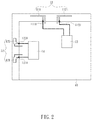
- FIG. 2 schematically shows the antenna assembly according to an embodiment of the present invention
- FIG. 3 schematically shows the low-frequency antenna unit of the antenna assembly in FIG. 2 ;
- FIG. 4 is a plot showing test results of the low-frequency antenna unit in FIG. 3 ;
- FIG. 5A shows Z-Y plane radiation patterns of the low-frequency antenna unit in FIG. 3 ;
- FIG. 5B shows X-Z plane radiation patterns of the low-frequency antenna unit in FIG. 3 ;
- FIG. 5C shows X-Y plane radiation patterns of the low-frequency antenna unit in FIG. 3 ;
- FIG. 6A schematically shows a low-frequency antenna unit of the present invention that has winding antennas
- FIG. 6B schematically shows a low-frequency antenna unit of the present invention that has bent antennas
- FIG. 6C schematically shows a low-frequency antenna unit of the present invention that has winding antennas with a rectangular region
- FIG. 7 schematically shows the high-frequency antenna unit of the antenna assembly in FIG. 2 ;
- FIG. 8 is a plot showing test results of the high-frequency antenna unit in FIG. 7 ;
- FIG. 9A shows Z-Y plane radiation patterns of the high-frequency antenna unit in FIG. 7 ;
- FIG. 9B shows X-Z plane radiation patterns of the high-frequency antenna unit in FIG. 7 ;
- FIG. 9C shows X-Y plane radiation patterns of the high-frequency antenna unit in FIG. 7 ;
- FIG. 10A schematically shows a high-frequency neutralization line of the present invention that has an assembled configuration
- FIG. 10B schematically shows a high-frequency neutralization line of the present invention that has a winding configuration
- FIG. 10C schematically shows a high-frequency neutralization line of the present invention that has a step-shaped configuration
- FIG. 11 is a plot showing test results of a low-frequency antenna unit of the present invention in relation to variation in width of the low-frequency neutralization line;
- FIG. 12 is a plot showing test results of a low-frequency antenna unit of the present invention in relation to variation in the grounding distance of the low-frequency neutralization line;
- FIG. 13 schematically shows an embodiment of the present invention whose low-frequency antenna unit and high-frequency antenna unit are located along the same edge of a circuit board;
- FIG. 14 schematically shows another embodiment of the low-frequency antenna unit of the present invention.
- the antenna assembly is a 2 ⁇ 2 MIMO antenna assembly by way of example and includes a circuit board 10 , at least one low-frequency antenna unit 11 , and at least one high-frequency antenna unit 12 .
- the circuit board 10 is provided with a low-frequency module 13 (e.g., a 2 GHz ⁇ 2.5 GHz antenna chip) and a high-frequency module 14 (e.g., a 5 GHz ⁇ 5.85 GHz antenna chip).
- the low-frequency antenna unit 11 is located at one edge of the circuit board 10 and is electrically connected to the low-frequency module 13 in order to operate in the 2 GHz ⁇ 2.5 GHz frequency band.
- the high-frequency antenna unit 12 is located at another edge of the circuit board 10 and is electrically connected to the high-frequency module 14 in order to operate in the 5 GHz ⁇ 5.85 GHz frequency band.
- the low-frequency antenna unit 11 is composed at least of a first low-frequency antenna 111 , a second low-frequency antenna 112 , and a low-frequency neutralization line 113 .
- the first low-frequency antenna 111 and the second low-frequency antenna 112 are spaced apart from each other and are arranged on one side (hereinafter referred to as the first side) of the circuit board 10 .
- the low-frequency antennas 111 and 112 are of the PIFA structure, with their respective grounding ends connected to the grounding surface of the circuit board 10 , and their respective feed ends 1111 and 1121 electrically and separately connected to the low-frequency module 13 .
- the low-frequency neutralization line 113 is arranged on the opposite side (hereinafter referred to as the second side) of the circuit board 10 .
- the two ends of the low-frequency neutralization line 113 correspond respectively to the first low-frequency antenna 111 and the second low-frequency antenna 112 in such a way that the two ends of the low-frequency neutralization line 113 overlap the two low-frequency antennas 111 and 112 respectively, as shown in FIG. 3 .
- the two ends of the low-frequency neutralization line 113 are electrically connected to the first low-frequency antenna 111 and the second low-frequency antenna 112 respectively.
- the two ends of the low-frequency neutralization line 113 are brought into contact with the two low-frequency antennas 111 and 112 respectively, thereby guiding one of the first low-frequency antenna 111 and the second low-frequency antenna 112 to couple electric current to the grounding surface and hence interfere less with the other of the first low-frequency antenna 111 and the second low-frequency antenna 112 .
- the low-frequency neutralization line 113 is connected between the low-frequency antennas 111 and 112 in an overlapping manner to isolate the low-frequency antennas 111 and 112 from each other, the low-frequency antennas 111 and 112 are closer to each other than if a conventional decoupling structure is used therebetween.
- the low-frequency neutralization line 113 lies within a region corresponding to the low-frequency antennas 111 and 112 and therefore occupies less area of the circuit board 10 than if arranged otherwise. It should be pointed out that the low-frequency neutralization line 113 is not on the same surface as the low-frequency antennas 111 and 112 and consequently not shown in FIG. 2 . When the circuit board 10 is a single-layer plate structure, the low-frequency antennas 111 and 112 and the low-frequency neutralization line 113 are located on the top and bottom sides of the circuit board 10 respectively, or vice versa.
- the low-frequency antennas 111 and 112 and the low-frequency neutralization line 113 are located in/on different layers of the circuit board 10 respectively. That is to say, the low-frequency antenna unit 11 may vary in configuration, provided that the “low-frequency antennas 111 and 112 ” and the “low-frequency neutralization line 113 ” do not lie completely on the same surface.
- the low-frequency antenna unit 11 shown in FIG. 2 and FIG. 3 , and the test results are plotted in FIG. 4 , in which it can be clearly seen that the low-frequency antennas 111 and 112 have an isolation of ⁇ 33 dB when the low-frequency antenna unit 11 operates in the 2.46 GHz, and an isolation of ⁇ 14 dB when the low-frequency antenna unit 11 operates in the 2.4 GHz band (2.415 GHz ⁇ 2.485 GHz).
- the low-frequency antenna unit 11 produces omnidirectional in the Z-Y plane (see FIG. 5A ), complementary in the X-Z plane (see FIG. 5B ) and X-Y plane (see FIG.
- the first low-frequency antenna and the second low-frequency antenna may be adjusted in configuration to meet product requirements, as shown by the low-frequency antenna units 11 A ⁇ 11 C in FIG. 6A to FIG. 6C .
- Each of the first low-frequency antennas 111 A ⁇ 111 C may have a “winding configuration” (i.e., with a plurality of bends), a “bent configuration” (i.e., with a single bend), or a “winding configuration with a rectangular region”, and so may each of the second low-frequency antennas 112 A ⁇ 112 C.
- the high-frequency antenna unit 12 is composed at least of a first high-frequency antenna 121 , a second high-frequency antenna 122 , and a high-frequency neutralization line 123 .
- the first high-frequency antenna 121 and the second high-frequency antenna 122 are spaced apart from each other and are arranged on the first side of the circuit board 10 (i.e., on the same side as the low-frequency antennas 111 and 112 ).
- the high-frequency antennas 121 and 122 are of the PIFA structure, with their respective grounding ends connected to the grounding surface of the circuit board 10 , and their respective feed ends 1211 and 1221 electrically and separately connected to the high-frequency module 14 .
- the high-frequency neutralization line 123 is arranged on the second side of the circuit board 10 (i.e., on the same side as the low-frequency neutralization line 113 ).
- the two ends of the high-frequency neutralization line 123 correspond respectively to the first high-frequency antenna 121 and the second high-frequency antenna 122 in such a way that the two ends of the high-frequency neutralization line 123 overlap the two high-frequency antennas 121 and 122 respectively, as shown in FIG. 7 .
- the two ends of the high-frequency neutralization line 123 are electrically connected to the first high-frequency antenna 121 and the second high-frequency antenna 122 respectively and are adjacent to the feed ends 1211 and 1221 of the first and the second high-frequency antennas 121 and 122 respectively; thus, the high-frequency neutralization line 123 isolates the high-frequency antennas 121 and 122 from each other. Moreover, with the high-frequency neutralization line 123 overlapping the first high-frequency antenna 121 and the second high-frequency antenna 122 , the high-frequency antennas 121 and 122 are closer to each other than if a conventional decoupling structure is used therebetween. In addition, the high-frequency neutralization line 123 lies within a region corresponding to the high-frequency antennas 121 and 122 and therefore occupies less area of the circuit board 10 than if arranged otherwise.
- the high-frequency antenna unit 12 shown in FIG. 2 and FIG. 7 The applicant tested the high-frequency antenna unit 12 shown in FIG. 2 and FIG. 7 , and the test results are plotted in FIG. 8 , in which it can be clearly seen that the high-frequency antennas 121 and 122 have an isolation of ⁇ 31 dB when the high-frequency antenna unit 12 operates in the 5.33 GHz, and an isolation of ⁇ 15 dB when the high-frequency antenna unit 12 operates in the 5 GHz band (5.15 GHz ⁇ 5.85 GHz).
- the high-frequency antenna unit 12 produces omnidirectional in the Z-Y plane(see FIG. 9A ), complementary in the X-Z plane (see FIG. 9B ) and X-Y plane(see FIG.
- the high-frequency neutralization line 123 as well as the first and the second high-frequency antennas may be adjusted in configuration to meet product requirements, as shown by the high-frequency antenna units 12 A ⁇ 12 C in FIG. 10A to FIG. 10C .
- Each of the high-frequency neutralization lines 123 A ⁇ 123 C may have an “assembled configuration” (i.e., composed of a plurality of elements interconnected), a “winding configuration” (i.e., with a plurality of bends), or a “step-shaped configuration”.
- the “assembled configuration” in which a plurality of elements are connected to one another
- the elements may be located in/on different layers of the circuit board, provided that the elements are electrically connected.
- the “step-shaped configuration” is formed by providing the high-frequency neutralization line 123 C with different widths, which in turn give rise to different phases respectively.
- the two antennas i.e., the first low-frequency antenna 111 and the second low-frequency antenna 112 ) of the low-frequency antenna unit 11 are located along the same edge of the circuit board 10
- the two antennas (i.e., the first high-frequency antenna 121 and the second high-frequency antenna 122 ) of the high-frequency antenna unit 12 are located along another edge of the circuit board 10 .
- a 4 ⁇ 4 MIMO antenna assembly for example, there will be one low-frequency antenna unit and one high-frequency antenna unit at each of two adjacent edges of the circuit board, and yet wire crossover will reduce than in a conventional antenna assembly where decoupling structures are used, thereby effectively avoiding an increase in signal attenuation or in RF loss to ensure the transmission quality of the antennas.
- the low-frequency neutralization line 113 and the high-frequency neutralization line 123 are so designed that each of the low-frequency antenna unit 11 and the high-frequency antenna unit 12 produces complementary radiation patterns that help maintain radiation efficiency.
- the configuration of the low-frequency neutralization line 113 may be adjusted to create the desired level of isolation in a specific working band.
- the low-frequency neutralization line 113 has a width W 1 and is spaced from the grounding surface by a grounding distance G 1 .
- a reduce in the width W 1 of the low-frequency neutralization line 113 with no change in the grounding distance G 1 leads to the test results in FIG. 11 of the low-frequency antenna unit 11 . It can be clearly seen in FIG.
- the high-frequency antenna unit 12 shows the same properties as stated above.
- the low-frequency antenna unit 11 and the high-frequency antenna unit 12 may be provided along the same edge of the circuit board 10 as depicted in FIG. 13 , in which the neutralization lines are not shown because they are not in/on the same layer as the antennas.
- the low-frequency antenna unit 11 D includes a first low-frequency antenna 111 D, a second low-frequency antenna 112 D, a first neutralization line 1131 D, and a second neutralization line 1132 D.
- the first low-frequency antenna 111 D and the first neutralization line 1131 D are located in/on different layers of the circuit board 10 respectively (e.g., on the top and bottom sides respectively, or vice versa).
- first neutralization line 1131 D is electrically connected to the first low-frequency antenna 111 D.
- the first neutralization line 1131 D and the second neutralization line 1132 D are also located in/on different layers of the circuit board 10 respectively.
- the other end of the first neutralization line 1131 D is electrically connected to one end of the second neutralization line 1132 D such that a low-frequency neutralization line 113 D (i.e., a neutralization line of an “assembled configuration”) is formed.
- the other end of the second neutralization line 1132 D is electrically connected to the second low-frequency antenna 112 D.
- the high-frequency antenna unit too, can use the structure described above.
- the antenna assemblies in the foregoing embodiments have two wireless antenna units (i.e., the low-frequency antenna unit 11 and the high-frequency antenna unit 12 ) by way of example only.
- the antenna assembly of the present invention may vary in configuration, provided that the circuit board 10 includes an antenna module (equivalent to the low-frequency module 13 or the high-frequency module 14 ), that the circuit board has one edge provided with at least one wireless antenna unit (equivalent to the low-frequency antenna unit 11 or the high-frequency antenna unit 12 ), and that the wireless antenna unit is composed of a first antenna of the PIFA structure, a second antenna of the PIFA structure, and a neutralization line, and has the structural features disclosed in the above embodiments (i.e., the first antenna and the second antenna are spaced apart from each other, and the two ends of the neutralization line correspond to the first antenna and the second antenna respectively in an overlapping manner and are electrically connected to the first antenna and the second antenna respectively to shorten layout traces and reduce the space occupied on the circuit board 10
Landscapes
- Physics & Mathematics (AREA)
- Electromagnetism (AREA)
- Variable-Direction Aerials And Aerial Arrays (AREA)
Abstract
Description
Claims (16)
Applications Claiming Priority (2)
| Application Number | Priority Date | Filing Date | Title |
|---|---|---|---|
| TW107205217U TWM566918U (en) | 2018-04-20 | 2018-04-20 | Antenna architecture with low trace path |
| TW107205217 | 2018-04-20 |
Publications (2)
| Publication Number | Publication Date |
|---|---|
| US20190326683A1 US20190326683A1 (en) | 2019-10-24 |
| US11088445B2 true US11088445B2 (en) | 2021-08-10 |
Family
ID=63518763
Family Applications (1)
| Application Number | Title | Priority Date | Filing Date |
|---|---|---|---|
| US16/238,632 Active 2040-02-13 US11088445B2 (en) | 2018-04-20 | 2019-01-03 | Antenna assembly with compact layout traces |
Country Status (3)
| Country | Link |
|---|---|
| US (1) | US11088445B2 (en) |
| JP (1) | JP3217955U (en) |
| TW (1) | TWM566918U (en) |
Families Citing this family (6)
| Publication number | Priority date | Publication date | Assignee | Title |
|---|---|---|---|---|
| CN109103597A (en) * | 2018-08-03 | 2018-12-28 | 瑞声精密制造科技(常州)有限公司 | Multiaerial system and mobile terminal |
| CN113036395B (en) * | 2019-12-09 | 2023-01-10 | 深圳市万普拉斯科技有限公司 | Antenna groups and communication equipment |
| CN111009722B (en) * | 2019-12-31 | 2024-12-03 | 朴海燕 | An integrated MIMO antenna system |
| US12476357B2 (en) * | 2020-12-21 | 2025-11-18 | Intel Corporation | Antenna assembly with isolation network |
| CN113851831B (en) * | 2021-08-26 | 2022-07-26 | 南京航空航天大学 | Miniaturized tightly-arranged MIMO antenna of 5G mobile terminal based on decoupling of patch capacitor |
| CN119009472A (en) * | 2023-05-18 | 2024-11-22 | 华为技术有限公司 | Antenna and communication equipment |
Citations (33)
| Publication number | Priority date | Publication date | Assignee | Title |
|---|---|---|---|---|
| US6624789B1 (en) * | 2002-04-11 | 2003-09-23 | Nokia Corporation | Method and system for improving isolation in radio-frequency antennas |
| CN2919565Y (en) | 2006-02-28 | 2007-07-04 | 华南理工大学 | Built-in triple-frequency mobile phone antenna based on multi-branched band spread technology |
| US20110115687A1 (en) * | 2009-11-13 | 2011-05-19 | Hsiao-Ting Huang | Printed Dual-band Antenna for Electronic Device |
| US20110175792A1 (en) * | 2010-01-21 | 2011-07-21 | Samsung Electronics Co. Ltd. | Apparatus for multiple antennas in wireless communication system |
| US20110237207A1 (en) * | 2010-03-23 | 2011-09-29 | Rf Micro Devices, Inc. | Adaptive antenna neutralization network |
| US20120013519A1 (en) * | 2010-07-15 | 2012-01-19 | Sony Ericsson Mobile Communications Ab | Multiple-input multiple-output (mimo) multi-band antennas with a conductive neutralization line for signal decoupling |
| CN102394384A (en) | 2011-07-19 | 2012-03-28 | 惠州Tcl移动通信有限公司 | Mobile equipment, mobile phone and antenna structure thereof |
| US20120075158A1 (en) | 2009-06-03 | 2012-03-29 | Murata Manufacturing Co., Ltd. | Antenna module |
| US20120212389A1 (en) * | 2011-02-21 | 2012-08-23 | Funai Electric Co, Ltd. | Multiantenna Unit and Communication Apparatus |
| US20120274532A1 (en) * | 2011-04-27 | 2012-11-01 | Fujitsu Component Limited | Antenna device and electronic device |
| US20130069842A1 (en) * | 2011-09-20 | 2013-03-21 | Samsung Electronics Co., Ltd. | Antenna apparatus for portable terminal |
| US20130271339A1 (en) * | 2012-04-17 | 2013-10-17 | Taiyo Yuden Co., Ltd. | Multi-antenna and electronic device |
| US20140347247A1 (en) * | 2013-05-27 | 2014-11-27 | Samsung Electronics Co., Ltd. | Antenna device for electronic device |
| CN204067572U (en) | 2014-07-09 | 2014-12-31 | 明泰科技股份有限公司 | Printed Monopole Antenna Using Trench to Suppress Frequency Bands |
| US20150042520A1 (en) * | 2013-07-30 | 2015-02-12 | Huawei Device Co., Ltd. | Wireless terminal |
| US20150214612A1 (en) * | 2014-01-27 | 2015-07-30 | Southern Taiwan University Of Science And Technology | High isolation electromagnetic transmitter and receiver |
| TW201547105A (en) | 2014-03-18 | 2015-12-16 | Galtronics Corp Ltd | Isolated ground for wireless device antenna |
| US9369187B1 (en) * | 2015-04-21 | 2016-06-14 | Amazon Technologies, Inc. | Antenna switching in an antenna system |
| US20160190700A1 (en) * | 2014-12-26 | 2016-06-30 | Realtek Semiconductor Corp. | Dualband antenna with isolation enhanced and method thereof |
| CN106025520A (en) | 2016-04-26 | 2016-10-12 | 威海市泓淋电子有限公司 | integrated module with antenna |
| CN205666327U (en) | 2016-06-08 | 2016-10-26 | 嘉善金昌电子有限公司 | Three -dimensional peviform stromatolite broadband antenna |
| US9543644B2 (en) * | 2014-07-01 | 2017-01-10 | The Chinese University Of Hong Kong | Method and an apparatus for decoupling multiple antennas in a compact antenna array |
| US20170012345A1 (en) * | 2014-01-24 | 2017-01-12 | Zte Corporation | Antenna Unit and Terminal |
| US9601826B2 (en) * | 2013-07-17 | 2017-03-21 | Zte Corporation | MIMO antenna, terminal and method for improving isolation |
| US20170084990A1 (en) * | 2014-05-19 | 2017-03-23 | Centre National De La Recherch Scientifique | Antenna system for reducing the electromagnetic coupling between antennas |
| CN107453031A (en) | 2016-05-31 | 2017-12-08 | 因派克伊莱克斯 | Vibration Pad Broadband Antenna for Vehicles |
| US20170358861A1 (en) | 2015-11-20 | 2017-12-14 | Taoglas Group Holdings Limited | Ten-frequency band antenna |
| US20180108984A1 (en) * | 2016-10-17 | 2018-04-19 | The Chinese University Of Hong Kong | Antenna Assembly and Self-Curing Decoupling Method for Reducing Mutual Coupling of Coupled Antennas |
| US20180151952A1 (en) * | 2015-05-19 | 2018-05-31 | Lg Innotek Co., Ltd. | Communication Module and Communication Device Including Same |
| US20180269578A1 (en) * | 2017-03-15 | 2018-09-20 | Arcadyan Technology Corporation | Antenna structure |
| US20190334254A1 (en) * | 2018-04-30 | 2019-10-31 | Arcadyan Technology Corporation | High-isolation dual-band antenna |
| US20190372215A1 (en) * | 2018-05-30 | 2019-12-05 | Wistron Neweb Corporation | Antenna structure |
| US20200021021A1 (en) * | 2018-07-12 | 2020-01-16 | Alpha Networks Inc. | Low-profile dual-band high-isolation antenna module |
-
2018
- 2018-04-20 TW TW107205217U patent/TWM566918U/en unknown
- 2018-06-29 JP JP2018002464U patent/JP3217955U/en active Active
-
2019
- 2019-01-03 US US16/238,632 patent/US11088445B2/en active Active
Patent Citations (36)
| Publication number | Priority date | Publication date | Assignee | Title |
|---|---|---|---|---|
| US6624789B1 (en) * | 2002-04-11 | 2003-09-23 | Nokia Corporation | Method and system for improving isolation in radio-frequency antennas |
| CN2919565Y (en) | 2006-02-28 | 2007-07-04 | 华南理工大学 | Built-in triple-frequency mobile phone antenna based on multi-branched band spread technology |
| US20120075158A1 (en) | 2009-06-03 | 2012-03-29 | Murata Manufacturing Co., Ltd. | Antenna module |
| US20110115687A1 (en) * | 2009-11-13 | 2011-05-19 | Hsiao-Ting Huang | Printed Dual-band Antenna for Electronic Device |
| US20110175792A1 (en) * | 2010-01-21 | 2011-07-21 | Samsung Electronics Co. Ltd. | Apparatus for multiple antennas in wireless communication system |
| US20110237207A1 (en) * | 2010-03-23 | 2011-09-29 | Rf Micro Devices, Inc. | Adaptive antenna neutralization network |
| US8780002B2 (en) * | 2010-07-15 | 2014-07-15 | Sony Corporation | Multiple-input multiple-output (MIMO) multi-band antennas with a conductive neutralization line for signal decoupling |
| US20120013519A1 (en) * | 2010-07-15 | 2012-01-19 | Sony Ericsson Mobile Communications Ab | Multiple-input multiple-output (mimo) multi-band antennas with a conductive neutralization line for signal decoupling |
| US20120212389A1 (en) * | 2011-02-21 | 2012-08-23 | Funai Electric Co, Ltd. | Multiantenna Unit and Communication Apparatus |
| US20120274532A1 (en) * | 2011-04-27 | 2012-11-01 | Fujitsu Component Limited | Antenna device and electronic device |
| CN102394384A (en) | 2011-07-19 | 2012-03-28 | 惠州Tcl移动通信有限公司 | Mobile equipment, mobile phone and antenna structure thereof |
| US20130069842A1 (en) * | 2011-09-20 | 2013-03-21 | Samsung Electronics Co., Ltd. | Antenna apparatus for portable terminal |
| US20130271339A1 (en) * | 2012-04-17 | 2013-10-17 | Taiyo Yuden Co., Ltd. | Multi-antenna and electronic device |
| US20140347247A1 (en) * | 2013-05-27 | 2014-11-27 | Samsung Electronics Co., Ltd. | Antenna device for electronic device |
| US9601826B2 (en) * | 2013-07-17 | 2017-03-21 | Zte Corporation | MIMO antenna, terminal and method for improving isolation |
| US20150042520A1 (en) * | 2013-07-30 | 2015-02-12 | Huawei Device Co., Ltd. | Wireless terminal |
| US20170012345A1 (en) * | 2014-01-24 | 2017-01-12 | Zte Corporation | Antenna Unit and Terminal |
| US20150214612A1 (en) * | 2014-01-27 | 2015-07-30 | Southern Taiwan University Of Science And Technology | High isolation electromagnetic transmitter and receiver |
| TW201547105A (en) | 2014-03-18 | 2015-12-16 | Galtronics Corp Ltd | Isolated ground for wireless device antenna |
| US10347984B2 (en) * | 2014-05-19 | 2019-07-09 | Universite De Nice Sophia Antipolis | Antenna system for reducing the electromagnetic coupling between antennas |
| US20170084990A1 (en) * | 2014-05-19 | 2017-03-23 | Centre National De La Recherch Scientifique | Antenna system for reducing the electromagnetic coupling between antennas |
| US9543644B2 (en) * | 2014-07-01 | 2017-01-10 | The Chinese University Of Hong Kong | Method and an apparatus for decoupling multiple antennas in a compact antenna array |
| CN204067572U (en) | 2014-07-09 | 2014-12-31 | 明泰科技股份有限公司 | Printed Monopole Antenna Using Trench to Suppress Frequency Bands |
| US20160190700A1 (en) * | 2014-12-26 | 2016-06-30 | Realtek Semiconductor Corp. | Dualband antenna with isolation enhanced and method thereof |
| US9369187B1 (en) * | 2015-04-21 | 2016-06-14 | Amazon Technologies, Inc. | Antenna switching in an antenna system |
| US20180151952A1 (en) * | 2015-05-19 | 2018-05-31 | Lg Innotek Co., Ltd. | Communication Module and Communication Device Including Same |
| US20170358861A1 (en) | 2015-11-20 | 2017-12-14 | Taoglas Group Holdings Limited | Ten-frequency band antenna |
| CN106025520A (en) | 2016-04-26 | 2016-10-12 | 威海市泓淋电子有限公司 | integrated module with antenna |
| CN107453031A (en) | 2016-05-31 | 2017-12-08 | 因派克伊莱克斯 | Vibration Pad Broadband Antenna for Vehicles |
| CN205666327U (en) | 2016-06-08 | 2016-10-26 | 嘉善金昌电子有限公司 | Three -dimensional peviform stromatolite broadband antenna |
| US20180108984A1 (en) * | 2016-10-17 | 2018-04-19 | The Chinese University Of Hong Kong | Antenna Assembly and Self-Curing Decoupling Method for Reducing Mutual Coupling of Coupled Antennas |
| US20180269578A1 (en) * | 2017-03-15 | 2018-09-20 | Arcadyan Technology Corporation | Antenna structure |
| US20190334254A1 (en) * | 2018-04-30 | 2019-10-31 | Arcadyan Technology Corporation | High-isolation dual-band antenna |
| US20190372215A1 (en) * | 2018-05-30 | 2019-12-05 | Wistron Neweb Corporation | Antenna structure |
| US20200021021A1 (en) * | 2018-07-12 | 2020-01-16 | Alpha Networks Inc. | Low-profile dual-band high-isolation antenna module |
| US10790583B2 (en) * | 2018-07-12 | 2020-09-29 | Alpha Networks Inc. | Low-profile dual-band high-isolation antenna module |
Also Published As
| Publication number | Publication date |
|---|---|
| JP3217955U (en) | 2018-09-13 |
| TWM566918U (en) | 2018-09-11 |
| US20190326683A1 (en) | 2019-10-24 |
Similar Documents
| Publication | Publication Date | Title |
|---|---|---|
| US11088445B2 (en) | Antenna assembly with compact layout traces | |
| US8659482B2 (en) | MIMO antenna having plurality of isolation adjustment portions | |
| US9312608B2 (en) | Multiple-input multiple-output antenna device | |
| US9337547B2 (en) | Internal antenna having wideband characteristic | |
| CN201655979U (en) | Combined type multi-input multi-output antenna module and system thereof | |
| US10790583B2 (en) | Low-profile dual-band high-isolation antenna module | |
| US10033088B2 (en) | Antenna unit and terminal | |
| JP3753436B2 (en) | Multiband printed monopole antenna | |
| JP6370363B2 (en) | Multi-antenna communication device | |
| JP6004692B2 (en) | ANTENNA DEVICE AND WIRELESS COMMUNICATION DEVICE | |
| US20050116869A1 (en) | Multi-band antenna structure | |
| CN104253303B (en) | Multiaerial system and mobile terminal | |
| EP3171455B1 (en) | Antenna module | |
| US12494586B2 (en) | Integrated multiple-antenna configuration and antenna module | |
| US12176602B2 (en) | Electronic device | |
| US20170170555A1 (en) | Decoupled Antennas For Wireless Communication | |
| JP2023543278A (en) | antenna device, array of antenna devices | |
| US20180287249A1 (en) | Antenna apparatus and electronic device | |
| CN114583448B (en) | A compact three-unit terminal MIMO antenna array for 5G mobile communications | |
| CN111129767B (en) | Dual-frequency antenna structure | |
| CN208522080U (en) | Antenna structure with low wiring path | |
| CN107845854B (en) | Composite antenna | |
| CN115764259B (en) | A double-sided MIMO antenna | |
| CN117134116B (en) | Antenna modules and communication equipment | |
| KR20250145231A (en) | An antenna device and a front end module using the same |
Legal Events
| Date | Code | Title | Description |
|---|---|---|---|
| AS | Assignment |
Owner name: ALPHA NETWORKS INC., TAIWAN Free format text: ASSIGNMENT OF ASSIGNORS INTEREST;ASSIGNORS:SU, DE-CHANG;YANG, CHIH-KAI;REEL/FRAME:047887/0508 Effective date: 20181228 |
|
| FEPP | Fee payment procedure |
Free format text: ENTITY STATUS SET TO UNDISCOUNTED (ORIGINAL EVENT CODE: BIG.); ENTITY STATUS OF PATENT OWNER: LARGE ENTITY |
|
| STPP | Information on status: patent application and granting procedure in general |
Free format text: NOTICE OF ALLOWANCE MAILED -- APPLICATION RECEIVED IN OFFICE OF PUBLICATIONS |
|
| STPP | Information on status: patent application and granting procedure in general |
Free format text: PUBLICATIONS -- ISSUE FEE PAYMENT RECEIVED |
|
| STPP | Information on status: patent application and granting procedure in general |
Free format text: PUBLICATIONS -- ISSUE FEE PAYMENT VERIFIED |
|
| STCF | Information on status: patent grant |
Free format text: PATENTED CASE |
|
| MAFP | Maintenance fee payment |
Free format text: PAYMENT OF MAINTENANCE FEE, 4TH YEAR, LARGE ENTITY (ORIGINAL EVENT CODE: M1551); ENTITY STATUS OF PATENT OWNER: LARGE ENTITY Year of fee payment: 4 |