US11088225B2 - Display device - Google Patents
Display device Download PDFInfo
- Publication number
- US11088225B2 US11088225B2 US16/637,817 US201916637817A US11088225B2 US 11088225 B2 US11088225 B2 US 11088225B2 US 201916637817 A US201916637817 A US 201916637817A US 11088225 B2 US11088225 B2 US 11088225B2
- Authority
- US
- United States
- Prior art keywords
- light transmitting
- region
- transmitting region
- disposed
- area
- Prior art date
- Legal status (The legal status is an assumption and is not a legal conclusion. Google has not performed a legal analysis and makes no representation as to the accuracy of the status listed.)
- Active, expires
Links
- 239000000758 substrate Substances 0.000 claims description 26
- 230000007704 transition Effects 0.000 description 22
- 238000002834 transmittance Methods 0.000 description 14
- 230000000694 effects Effects 0.000 description 6
- 238000000034 method Methods 0.000 description 6
- 230000008569 process Effects 0.000 description 6
- 238000005516 engineering process Methods 0.000 description 4
- 239000010408 film Substances 0.000 description 3
- -1 indium tin metal oxide Chemical class 0.000 description 3
- 239000000463 material Substances 0.000 description 3
- 229910044991 metal oxide Inorganic materials 0.000 description 3
- BQCADISMDOOEFD-UHFFFAOYSA-N Silver Chemical compound [Ag] BQCADISMDOOEFD-UHFFFAOYSA-N 0.000 description 2
- 230000009286 beneficial effect Effects 0.000 description 2
- 230000008859 change Effects 0.000 description 2
- 238000004519 manufacturing process Methods 0.000 description 2
- 238000012986 modification Methods 0.000 description 2
- 230000004048 modification Effects 0.000 description 2
- 230000002093 peripheral effect Effects 0.000 description 2
- 229910052581 Si3N4 Inorganic materials 0.000 description 1
- VYPSYNLAJGMNEJ-UHFFFAOYSA-N Silicium dioxide Chemical compound O=[Si]=O VYPSYNLAJGMNEJ-UHFFFAOYSA-N 0.000 description 1
- 230000005540 biological transmission Effects 0.000 description 1
- 239000003990 capacitor Substances 0.000 description 1
- 239000006185 dispersion Substances 0.000 description 1
- 230000001788 irregular Effects 0.000 description 1
- 230000003287 optical effect Effects 0.000 description 1
- HQVNEWCFYHHQES-UHFFFAOYSA-N silicon nitride Chemical compound N12[Si]34N5[Si]62N3[Si]51N64 HQVNEWCFYHHQES-UHFFFAOYSA-N 0.000 description 1
- 229910052814 silicon oxide Inorganic materials 0.000 description 1
- 229910052709 silver Inorganic materials 0.000 description 1
- 239000004332 silver Substances 0.000 description 1
- 239000010409 thin film Substances 0.000 description 1
- 239000012780 transparent material Substances 0.000 description 1
Images


Classifications
-
- H01L27/3234—
-
- H—ELECTRICITY
- H10—SEMICONDUCTOR DEVICES; ELECTRIC SOLID-STATE DEVICES NOT OTHERWISE PROVIDED FOR
- H10K—ORGANIC ELECTRIC SOLID-STATE DEVICES
- H10K59/00—Integrated devices, or assemblies of multiple devices, comprising at least one organic light-emitting element covered by group H10K50/00
- H10K59/60—OLEDs integrated with inorganic light-sensitive elements, e.g. with inorganic solar cells or inorganic photodiodes
- H10K59/65—OLEDs integrated with inorganic image sensors
-
- H01L27/3244—
-
- H01L51/5209—
-
- H—ELECTRICITY
- H10—SEMICONDUCTOR DEVICES; ELECTRIC SOLID-STATE DEVICES NOT OTHERWISE PROVIDED FOR
- H10K—ORGANIC ELECTRIC SOLID-STATE DEVICES
- H10K50/00—Organic light-emitting devices
- H10K50/80—Constructional details
- H10K50/805—Electrodes
- H10K50/81—Anodes
- H10K50/813—Anodes characterised by their shape
-
- H—ELECTRICITY
- H10—SEMICONDUCTOR DEVICES; ELECTRIC SOLID-STATE DEVICES NOT OTHERWISE PROVIDED FOR
- H10K—ORGANIC ELECTRIC SOLID-STATE DEVICES
- H10K59/00—Integrated devices, or assemblies of multiple devices, comprising at least one organic light-emitting element covered by group H10K50/00
- H10K59/10—OLED displays
- H10K59/12—Active-matrix OLED [AMOLED] displays
-
- H—ELECTRICITY
- H10—SEMICONDUCTOR DEVICES; ELECTRIC SOLID-STATE DEVICES NOT OTHERWISE PROVIDED FOR
- H10K—ORGANIC ELECTRIC SOLID-STATE DEVICES
- H10K59/00—Integrated devices, or assemblies of multiple devices, comprising at least one organic light-emitting element covered by group H10K50/00
- H10K59/80—Constructional details
- H10K59/805—Electrodes
- H10K59/8051—Anodes
- H10K59/80515—Anodes characterised by their shape
-
- H—ELECTRICITY
- H10—SEMICONDUCTOR DEVICES; ELECTRIC SOLID-STATE DEVICES NOT OTHERWISE PROVIDED FOR
- H10K—ORGANIC ELECTRIC SOLID-STATE DEVICES
- H10K59/00—Integrated devices, or assemblies of multiple devices, comprising at least one organic light-emitting element covered by group H10K50/00
- H10K59/10—OLED displays
- H10K59/12—Active-matrix OLED [AMOLED] displays
- H10K59/131—Interconnections, e.g. wiring lines or terminals
Definitions
- the present invention relates to the field of display technologies, and in particular, to a display device.
- a display device comprises a display panel.
- the display panel comprises a main display region and a function additional region, and at least a portion of the function additional region is surrounding by the main display region;
- a plurality of first pixels are arranged in the function additional region, at least one light transmitting region is disposed in the function additional region, and an area of each of the light transmitting regions is greater than or equal to 0.32 square millimeters (mm2);
- an overall shape of the light transmitting region is circular, large semicircular or small semicircular, and a length of a diameter of the light transmitting region is 1.0 to 10 mm; or the overall shape of the light transmitting region is a regular polygon, a short side of the light transmitting region has a length of 1.0 to 10 mm, and a long side of the light transmitting region has a length of 1.5 to 200 mm.
- each of the light transmitting region is less than or equal to 120 mm 2 .
- each of the light transmitting region is 0.36 to 100 mm 2 .
- a first anode for driving the first pixel is provided in at least one of the light transmitting region, a sum of the areas of all of the first anodes disposed in the light transmitting region is less than or equal to 50% of the area of the corresponding light transmitting region.
- the sum of the areas of all of the first anodes disposed in the light transmitting region is greater than or equal to 5% of the area of the corresponding light transmitting region.
- the display device further comprises a substrate and a plurality of first driving circuits disposed on the substrate, and the first driving circuits disposed at a periphery of the light transmitting region.
- the display panel further comprises at least two insulating layers disposed on the substrate, the first driving circuit is disposed on the substrate and covers by the insulating layers, and the first driving circuit and the first anode is electrically connected through a transparent wire disposed in at least two of the insulating layers.
- a plurality of second pixels are disposed in the main display region, a second driving circuit disposed in the main display region is disposed on the substrate, and the second pixels are electrically connected to the second driving circuit through a conductive layer disposed in at least two layers of the insulating layer.
- each of the light transmitting region is greater than or equal to 50 times an area of each of the second pixels, and the area of each of the light transmitting region is less than or equal to 210,000 times the area of each of the second pixels.
- a display device comprises a display panel.
- the display panel comprises a main display region and a function additional region, and at least a portion of the function additional region is surrounding by the main display region;
- a plurality of first pixels are arranged in the function additional region, at least one light transmitting region is disposed in the function additional region, and an area of each of the light transmitting regions is greater than or equal to 0.32 square millimeters (mm2).
- each of the light transmitting region is less than or equal to 120 mm 2 .
- each of the light transmitting region is 0.36 to 100 mm 2 .
- a first anode for driving the first pixel is provided in at least one of the light transmitting region, a sum of the areas of all of the first anodes disposed in the light transmitting region is less than or equal to 50% of the area of the corresponding light transmitting region.
- the sum of the areas of all of the first anodes disposed in the light transmitting region is greater than or equal to 5% of the area of the corresponding light transmitting region.
- the display device further comprises a substrate and a plurality of first driving circuits disposed on the substrate, and the first driving circuits disposed at a periphery of the light transmitting region.
- the display panel further comprises at least two insulating layers disposed on the substrate, the first driving circuit is disposed on the substrate and covers by the insulating layers, and the first driving circuit and the first anode is electrically connected through a transparent wire disposed in at least two of the insulating layers.
- a plurality of second pixels are disposed in the main display region, a second driving circuit disposed in the main display region is disposed on the substrate, and the second pixels are electrically connected to the second driving circuit through a conductive layer disposed in at least two layers of the insulating layer.
- each of the light transmitting region is greater than or equal to 50 times an area of each of the second pixels, and the area of each of the light transmitting region is less than or equal to 210,000 times the area of each of the second pixels.
- an overall shape of the light transmitting region is circular, large semicircular or small semicircular, and a length of a diameter of the light transmitting region is 1.0 to 10 mm.
- an overall shape of the light transmitting region is a regular polygon, a short side of the light transmitting region has a length of 1.0 to 10 mm, and a long side of the light transmitting region has a length of 1.5 to 200 mm.
- a function additional region can be used for displaying images, so that a display panel can display an effect of a full-screen display, and can also be used for installing photosensitive elements such as a camera to improve user experience.
- FIG. 1 is a schematic view of a display panel according to an embodiment of the present invention.
- FIG. 2 is a schematic structural view of the display panel according to an embodiment of the present invention.
- FIG. 3 is a schematic view showing an overall shape of a light transmitting region in a circular shape according to an embodiment of the present invention.
- FIG. 4 is a schematic view showing the overall shape of the light transmitting region in a semicircular shape according to an embodiment of the present invention.
- FIG. 5 is a schematic view showing the overall shape of the light transmitting region in a small semicircular shape according to an embodiment of the present invention.
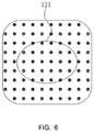
- FIG. 6 is a schematic view showing the overall shape of the light transmitting region in an elliptical shape according to an embodiment of the present invention.
- FIG. 7 is a schematic view showing the overall shape of the light transmitting region in a substantially semi-elliptical shape according to an embodiment of the present invention.
- FIG. 8 is a schematic view showing the overall shape of the light transmitting region in a small semi-elliptical shape according to an embodiment of the present invention.
- FIG. 9 is a schematic view showing the overall shape of the light transmitting region in a rectangular shape according to an embodiment of the present invention.
- FIG. 10 is a schematic view showing a plurality of light transmitting regions in an embodiment of the present invention.
- FIG. 11 and FIG. 12 are schematic views showing an arrangement of a driving circuit and a signal line according to an embodiment of the present invention.
- FIG. 13 and FIG. 14 are schematic views showing an arrangement of a driving circuit and a signal line according to another embodiment of the present invention.
- FIG. 15 and FIG. 16 are schematic views showing an arrangement of a driving circuit and a signal line according to yet another embodiment of the present invention.
- the present invention is directed to a technical problem of a current OLED display panel, which is: in the current OLED display panel using an under-screen camera, a camera area does not display images, and an effect of full-screen display cannot be presented, which affects user experience.
- a display device as shown in FIG. 1 , the display device comprises a display panel 10 .
- the display panel 10 comprises a main display region 11 and a function additional region 12 , and at least a portion of the function additional region 12 is surrounding by the main display region 11 .
- the display panel 10 can be a full-screen display panel 10 , a plurality of first pixels 122 are arranged in the function additional region 12 , and a plurality of second pixels 111 are arranged in the main display region 11 .
- the main display region 11 can display images, and the function additional region 12 can be disposed at any position of the display panel 10 .
- the function additional region 12 can be used for displaying the images, so that the display panel 10 can exhibit the effect of a full-screen display, and the function additional region 12 can also be used for mounting photosensitive elements such as a camera, an optical touch component, and a fingerprint recognition sensor, thereby improving the user experience.
- a pixel density in the function additional region 12 may be the same as or different from a pixel density in the main display region 11 .
- Display brightness at the function additional region 12 may be the same as or different from display brightness at the main display region 11 .
- each first pixels 122 comprises a first red sub-pixel, a first blue sub-pixel, and a first green sub-pixel; and each second pixels 111 comprises a second red sub-pixel, a second blue sub-pixel, and a second green sub-pixel.
- the function additional region 12 is provided with at least one light transmitting region 121 , and the plurality of first pixels 122 are arranged in the light transmitting region 121 .
- the light transmitting region 121 is used to increase an overall transmittance of the function additional region 12 , thereby ensuring the overall transmittance of the function additional region 12 and realizing good display and camera functions in the function additional region 12 to enhance the user experience.
- the display panel 10 comprises a substrate 50 , a plurality of first driving circuits 1221 disposed on the substrate 50 and disposed at a periphery of the light transmitting region 121 , and at least two insulating layers disposed on the substrate 50 .
- the first driving circuits 1221 are covered by the insulating layers.
- the first driving circuits 1221 and the first anode 1222 are electrically connected by a transparent wire disposed in the at least two insulating layers.
- the transparent wire comprises at least two connecting wires at different layers.
- the substrate 50 is provided with a second driving circuit 1112 disposed in the main display region 11 .
- the second pixel 111 is electrically connected to the second driving circuit 1112 through a conductive layer disposed in at least two layers of the insulating layer.
- the display panel 10 comprises the first driving circuit 1221 disposed on the substrate 50 , a first insulating layer 61 covering the first driving circuit 1221 , a first overlapping line 71 disposed on the first insulating layer 61 , a second insulating layer 62 covering the first overlapping line 71 , a second overlapping line 72 disposed on the second insulating layer 62 , a third insulating layer 63 covering the second overlapping line 72 , a third overlapping line 73 disposed on the third insulating layer 63 , a fourth insulating layer 64 covering the second overlapping line 72 , and a pixel anode and a pixel definition layer 80 disposed on the fourth insulating layer 64 .
- the pixel definition layer 80 has a pixel opening 81 corresponding to the pixel anode.
- the overlapping line disposed in the light transmitting region 121 is a transparent wire.
- the overlapping lines disposed at different layers are electrically connected through vias.
- the electrical connection between the first anode 1222 and the first driving circuit 1221 is realized by electrical connection of the overlapping lines disposed in different layers, thereby facilitating wiring arrangement.
- spacings between two adjacent overlapping lines on the same layer is greater than 2 micrometers to prevent short circuit between two adjacent overlapping lines on the same layer.
- Line width of each overlapping line is greater than 1 micron.
- the pixel anode comprises the first anode 1222 and a second anode 1111 for driving the second pixel 111 .
- the second anode 1111 is disposed in the main display region 11 .
- a conductive layer may be the same as a structure and a process of the transparent wire, and the second anode 1111 is electrically connected to the second driving circuit 1112 through a plurality of overlapping lines.
- the conductive layer may also be formed by multiple layers of opaque conductive lines disposed in the main display region 11 . That is, the overlapping lines disposed in the main display region 11 are opaque conductive lines.
- FIG. 2 only shows the case that the first anode 1222 is electrically connected to the first driving circuit 1221 through the overlapping lines disposed in the light transmitting region 121 .
- the first anode 1222 can also be electrically connected to the first driving circuit 1221 through overlapping lines disposed at other regions in the function additional region 12 or overlapping lines in the main display region 11 .
- FIG. 2 only shows the case of having three overlapping lines. In actual implementation, it can also be set to two, four, five, or more layers of overlapping lines.
- manufacturing materials of the transparent wire include, but are not limited to, indium tin metal oxide, indium zinc metal oxide, fluorine tin metal oxide, or nano silver wire.
- the insulating layer is made of a transparent material including, but not limited to, silicon oxide or silicon nitride.
- an area of each of the light transmitting regions 121 is greater than or equal to 0.32 square millimeters.
- an arrangement of the light transmitting regions 121 can increase the transmittance of the function additional region 12 .
- the driving of the first pixels 122 requires a transparent wire electrically connected thereto. The larger the area of the light transmitting region 121 is, the smaller the interference and diffraction of the transparent wire for driving the first pixels 122 can be reduced to, thereby improving a usage effect of the photosensitive elements such as the camera.
- the area of each of the light transmitting regions 121 is less than or equal to 120 square millimeters.
- each of the light transmitting regions 121 has the area of 0.36 to 100 square millimeters.
- the area of each of the light transmitting regions 121 may be 0.5 square millimeters, 2 square millimeters, 10 square millimeters, 20 square millimeters, 50 square millimeters, or 80 square millimeters, which are not enumerated here.
- the area of the light transmitting region 121 can be set as large as possible according to the actual area of the function additional region 12 .
- the area of the light transmitting region 121 may be 120 square millimeters.
- the area of the light transmitting region 121 can be set as large as possible according to the actual area of the function additional region 12 . It can be understood that the greater the number of the light transmitting regions 121 is, the smaller the area of each light transmitting regions 121 is.
- the area of each of the light transmitting regions 121 is greater than or equal to 50 times an area of each of the second pixels 111 .
- each of the light transmitting regions 121 is less than or equal to 210,000 times the area of each of the second pixels 111 .
- each of the light transmitting regions 121 is 70 to 200,000 times the area of each of the second pixels 111 .
- the area of each of the light transmitting region 121 may be 100 times, 500 times, 1,000 times, 5,000 times, 10,000 times, or 50,000 times the area of each of the second pixels 111 , which are not enumerated here.
- a first anode 1222 for driving the first pixel 122 is disposed in at least one of the light transmitting regions 121 .
- a sum of the areas of all the first anodes 1222 disposed in the light transmitting region 121 is less than or equal to 50% of the area of the corresponding light transmitting region 121 .
- the sum of the areas of all the first anodes 1222 disposed in the light transmitting region 121 is greater than or equal to 5% of the area of the corresponding light transmitting regions 121 .
- a portion of the first anode 1222 may be blocked by the pixel definition layer 80 .
- a sum of areas of portions of the first anode 1222 that are not blocked by the pixel definition layer 80 in the light transmitting region 121 is less than or equal to 50% of the area of the corresponding light transmitting region 121 .
- a manufacturing material of the first anode 1222 generally comprises an opaque material, such as a first transparent conductive film layer, a silver film layer, and a second transparent conductive film layer that are stacked.
- the first anode 1222 is prevented from affecting the display of the light transmitting region 121 through limiting the area of the light transmitting region 121 of the first anode 1222 and ensuring a density of the first pixel 122 .
- the overall transmittance of the function additional region 12 can also be improved.
- the overall shape of the light transmitting region 121 is circular (as shown in FIG. 3 ), large semicircular (as shown in FIG. 4 ), or small semicircular (as shown in FIG. 5 ).
- a length of a diameter of the light transmitting region 121 is 1.0 to 10 mm.
- the length of the diameter of the light transmitting region 121 may be 1 mm, 2 mm, 5 mm, or other values, which are not enumerated here.
- the overall shape of the light transmitting region 121 is elliptical (as shown in FIG. 6 ), large semi-elliptical (as shown in FIG. 7 ), or small semi-elliptical (as shown in FIG. 8 ).
- a length of a short axis of the light transmitting region 121 is 1.0 to 10 mm, and a length of a long axis is 1.5 to 200 mm.
- the length of the short axis of the light transmitting region 121 may be 1 mm, 2 mm, 5 mm, or other values, which are not enumerated here.
- the length of the long axis can be 1.5 mm, 2 mm, 5 mm, 20 mm, 50 mm, 100 mm, which are not enumerated here.
- the overall shape of the light transmitting region 121 may also be a regular polygon, such as a rectangle (as shown in FIG. 9 ), a triangle, or a pentagon, etc.
- the short side of the light transmitting region 121 has a length of 1.0 to 10 mm, and the long side has a length of 1.5 to 200 mm.
- the overall shape of the light transmitting region 121 may also be a square shape, a rounded rectangle, or an irregular polygon, which are not enumerated here.
- the pixel density in the function additional region 12 may be increased according to actual needs to facilitate driving the first pixel 122 , and two or three or more light transmitting regions 121 may be disposed in the function additional region 12 due to factors such as limitation of process conditions.
- the plurality of light transmitting regions 121 are spaced apart from each other. Each of the light transmitting regions 121 is provided with the first pixel 122 .
- the first driving circuit 1221 and the signal line are distributed on a peripheral side of each of the light transmitting regions 121 .
- the first driving circuit 1221 is electrically connected to the first pixel 122 for driving the first pixel 122 .
- the light transmitting regions 121 may be arranged in an array or randomly distributed.
- FIG. 11 only shows the case that all of the light transmitting regions 121 are circular in shape.
- the shape of the light transmitting region 121 may be any of the above-listed shapes, and all of the light transmitting regions 121 may have the same shape or different shapes.
- the number of the light transmitting regions 121 can be selected according to the shape and size of the function additional region 12 and the preset area of the light transmitting region 121 in the actual implementation.
- the overall transmittance of the function additional region 12 is related to the number of the light transmitting regions 121 .
- the opaqueness of the first driving circuit 1221 and the signal line cause the transmittance to decrease. Therefore, in an embodiment, only one light transmitting region 121 may be disposed in the function additional region 12 , during which the single hole area of the light transmitting region 121 is the largest, and the overall transmittance of the function additional region 12 is the highest.
- the peripheral side of the light transmitting region 121 is provided with a plurality of pixel driving circuit islands 30 and signal lines formed by pixel driving circuits.
- the pixel driving circuit island 30 comprises the first driving circuit 1221 .
- the signal line is electrically connected to the first driving circuit 1221 to input various electrical signals to the pixel driving circuit island 30 .
- the pixel driving circuit island 30 and the signal line are not disposed in the light transmitting region 121 .
- the setting of the first driving circuit 1221 needs to occupy an area of a certain region.
- the area size of the light transmitting region 121 can be increased.
- the first driving circuit 1221 and the signal line for driving the first pixel 122 are disposed on a circumferential side of the light transmitting region 121 to ensure that the pixel driving circuit island 30 is not required to be disposed in the light transmitting region 121 , thereby preventing the first driving circuit 1221 and signal lines from affecting the display and light transmission of the light transmitting region 121 .
- first anode 1222 disposed in at least a portion of the light transmitting region 121 means that the first anode 1222 is disposed in one light transmitting region 121 or disposed in the plurality of light transmitting regions 121 . In an actual implementation, the first anode 1222 may also be disposed in all of the light transmitting regions 121 .
- the first driving circuit 1221 can be used to drive the plurality of first pixels 122 in the light transmitting region 121 to ensure that no driving circuit is disposed in the light transmitting region 121 , so that the light transmitting region 121 has a high transmittance.
- the first driving circuit 1221 can also be used to drive the first pixels 122 in the area other than the light transmitting region 121 in the function additional region 12 .
- first driving circuit 1221 and the signal lines may be disposed in the function additional region 12 , or may be disposed in the main display region 11 .
- the pixel driving circuit island 30 may also be responsible for driving a portion of the second pixel 111 in the main display region 11 near the function additional region 12 .
- each of the pixel driving circuit islands 30 is formed by collectively gathering a plurality of pixel driving circuits in an island shape, and the concentrated gathering is compared with the dispersion of the pixel driving circuits in the conventional technology. That is, one pixel driving circuit corresponding to one pixel in the conventional technology.
- the pixel driving circuit comprises a plurality of switching elements, capacitors, signal lines, etc., and the switching elements may be thin film transistors, diodes or other devices.
- the signal lines comprise a plurality of first signal lines 41 and a plurality of second signal lines 42 .
- the first signal lines 41 and the second signal lines 42 are electrically connected to the pixel driving circuit islands 30 to input various electrical signals to the pixel driving circuit islands 30 .
- the pixel driving circuit island 30 is electrically connected to the first anode 1222 through a transparent wire to transmit an electrical signal to the first anode 1222 .
- the first signal line 41 may comprise at least one of a scan line, an illuminating signal line for controlling the illuminating of the OLED, and a reset line for controlling the anode reset of the OLED.
- Each of the first signal lines 41 comprises a first straight line section 411 , a first bypass section 413 , and a first transition section 412 .
- the display panel 10 further comprises a plurality of first sector regions 21 and a plurality of second sector regions 22 .
- the first sector region 21 is a region defined by a plurality of the first transition sections 412 in a fan-shaped arrangement
- the second sector region 22 is a region defined by a plurality of the second transition sections 422 in a fan-shaped arrangement.
- the plurality of first straight line sections 411 are horizontally arranged in parallel, the first transition section 412 is disposed in the first sector region 21 , and the plurality of first transition sections 412 are fan-shaped in the first sector region 21 .
- the first straight line section 411 extends to the first sector region 21 and is electrically connected to the first transition section 412 , so that the plurality of first signal lines 41 are integrated with the plurality of sets of first signal lines 41 , and thus change an extended path of the plurality of sets of first signal lines 41 to avoid the function additional region 12 .
- a spacing between two adjacent first transition sections 412 in the first sector section 21 is less than a spacing between adjacent two first straight line sections 411 .
- the plurality of first transition sections 412 of the first sector region 21 may be divided into at least two layers.
- the first bypass section 413 is electrically connected to all of the pixel drive circuit islands 30 in the first group of the pixel driving circuit island 30 in sequence.
- the first bypass section 413 can be a straight line, an arc, or a plurality of polygonal sections.
- the second signal line 42 may comprise data lines.
- Each of the second signal lines 42 comprises a second straight line section 421 , a second bypass section 423 , and a second transition section 422 .
- the plurality of second straight line sections 421 of the plurality of second signal lines 42 are vertically arranged in parallel.
- the second transition section 422 is disposed in the second sector region 22 , and the plurality of second transition sections 422 are fan-shaped in the second sector region 22 .
- the second straight line section 421 extends to the second sector region 22 and is electrically connected to the second transition section 422 , so that the plurality of second signal lines 42 are integrated with the plurality of sets of second signal lines 42 , and thus change an extended path of the plurality of sets of second signal lines 42 to avoid the function additional region 12 .
- a spacing between adjacent two second transition sections 422 in the second sector region 22 is less than a spacing between adjacent two second straight line sections 421 .
- the plurality of second straight line sections 421 of the plurality of second signal lines 42 are divided into a plurality of clusters respectively extending to the plurality of second sector regions 22 to be electrically connected to the plurality of second transition sections 422 .
- Each cluster of the first straight line section 411 correspondingly extends into the second sector region 22 .
- the plurality of second transition sections 422 are divided into a plurality of clusters, and each cluster of second transition sections 422 is disposed in the same second sector region 22 .
- the plurality of second sector regions 22 are symmetrically disposed on opposite sides of the function additional region 12 and disposed adjacent to the first bypass line.
- the second bypass section 423 of the plurality of second signal lines 42 is disposed at the edge of the function addition region 12 .
- the second transition section 422 is electrically connected to the second bypass section 423 one-to-one.
- the first bypass section 413 and the second bypass section 423 are disposed at different layers.
- the two ends of the second bypass section 423 are electrically connected to the second transition section 422 . That is, the second bypass section 423 is electrically connected to the second transition section 422 .
- a plurality of the first bypass sections 413 , a plurality of the second bypass sections 423 , and at least a portion of the pixel driving circuit islands 30 are formed as the light transmitting region 121 .
- the light transmitting region 121 is convex or concave corresponding to an edge of the first group of pixel driving circuit islands 30 at the edge of the first bypass section 413 to increase a light transmissive area of the function additional region 12 .
- the display panel 10 further comprises a plurality of connecting lines 90 .
- the connecting line 90 and the second bypass section 423 are disposed in different layers, and each set of the second bypass section 423 comprises at least two second bypass sections 423 having different lengths.
- the two ends of the second bypass section 423 of each cluster are respectively electrically connected to the pixel driving circuit islands 30 of the first group of pixel driving circuit islands 30 which are mutually mirrored by the connecting line 90 , so as to prevent the same group of two adjacent clusters of second bypass sections 423 from experiencing short circuits during the extension process in order to achieve electrical connection with the pixel driving circuit islands 30 .
- the display panel 10 shown in FIG. 13 is basically similar in structure to the display panel 10 shown in FIG. 11 , except that the second bypass section 423 of the second signal line 42 is arranged in an arc.
- the second bypass section 423 of the second signal line 42 is disposed in a circular arc line, and the overall shape of the light transmitting region 121 is circular.
- the second bypass section 423 of the second signal line 42 is disposed in an elliptical arc, and the overall shape of the light transmitting region 121 is elliptical.
- the display panel 10 shown in FIG. 15 is substantially similar in structure to the display panel 10 shown in FIG. 11 , except that at least a portion of the second bypass section 423 of the second signal line 42 is disposed around the entire light transmitting region 121 .
- a portion of the pixel driving circuit islands 30 are uniformly arranged in a ring shape at the edge of the light transmitting region 121 .
- the second bypass sections 423 of the plurality of second signal lines 42 are disposed around the light transmitting region 121 and are electrically connected to at least a portion of the pixel driving circuit islands 30 .
- the first bypass sections 413 of the plurality of first signal lines 41 are electrically connected to any two adjacent pixel driving circuit islands 30 of the pixel driving circuit islands 30 in sequence.
- a pixel driving circuit is disposed under each of the display sub-pixels, so that the plurality of pixel driving circuits corresponding to the plurality of display pixels are distributedly distributed.
- the first driving circuit 1211 in the pixel driving circuit island 30 is used to drive the plurality of first pixels 122 in the light transmitting region 121 so that no pixel driving circuit is provided in the light transmitting region 121 , thereby improving the transmittance of the light transmitting region 121 .
- the arrangement of the plurality of pixel driving circuit islands 30 also increases the size of the light transmitting region 121 .
- the plurality of first signal lines 41 and the plurality of second signal lines 42 are disposed on the periphery of the light transmitting region 121 in cooperation with the plurality of pixel driving circuit islands 30 to further improve the transmittance of the light transmitting region 121 .
- the beneficial effects of the invention are: by properly setting the shapes and the areas of the light transmitting region 121 , and limiting the area of the first anode 1222 disposed in the light transmitting region 121 , the overall transmittance of the functional additional region 12 is improved.
- the function additional region 12 can be used for displaying the images, so that the display panel 10 can display the effect of the full-screen display, and can also be used for installing the photosensitive elements such as the camera to improve the user experience.
Landscapes
- Chemical & Material Sciences (AREA)
- Inorganic Chemistry (AREA)
- Life Sciences & Earth Sciences (AREA)
- Sustainable Development (AREA)
- Physics & Mathematics (AREA)
- Optics & Photonics (AREA)
- Engineering & Computer Science (AREA)
- Microelectronics & Electronic Packaging (AREA)
- Devices For Indicating Variable Information By Combining Individual Elements (AREA)
- Electroluminescent Light Sources (AREA)
Abstract
Description
Claims (20)
Applications Claiming Priority (3)
| Application Number | Priority Date | Filing Date | Title |
|---|---|---|---|
| CN201910735413.7A CN110492018B (en) | 2019-08-09 | 2019-08-09 | Display device |
| CN201910735413.7 | 2019-08-09 | ||
| PCT/CN2019/116101 WO2021027106A1 (en) | 2019-08-09 | 2019-11-06 | Display apparatus |
Related Parent Applications (1)
| Application Number | Title | Priority Date | Filing Date |
|---|---|---|---|
| PCT/CN2019/116101 Substitution WO2021027106A1 (en) | 2019-08-09 | 2019-11-06 | Display apparatus |
Publications (2)
| Publication Number | Publication Date |
|---|---|
| US20210043702A1 US20210043702A1 (en) | 2021-02-11 |
| US11088225B2 true US11088225B2 (en) | 2021-08-10 |
Family
ID=74498711
Family Applications (1)
| Application Number | Title | Priority Date | Filing Date |
|---|---|---|---|
| US16/637,817 Active 2040-01-07 US11088225B2 (en) | 2019-08-09 | 2019-11-06 | Display device |
Country Status (1)
| Country | Link |
|---|---|
| US (1) | US11088225B2 (en) |
Families Citing this family (3)
| Publication number | Priority date | Publication date | Assignee | Title |
|---|---|---|---|---|
| CN113097283A (en) * | 2021-04-06 | 2021-07-09 | 京东方科技集团股份有限公司 | Display panel, manufacturing method thereof and display device |
| CN115241227A (en) * | 2021-04-23 | 2022-10-25 | 深圳市柔宇科技股份有限公司 | A display panel and display device |
| CN113823210B (en) * | 2021-08-19 | 2023-06-27 | 武汉华星光电半导体显示技术有限公司 | Display panel and display device |
Citations (1)
| Publication number | Priority date | Publication date | Assignee | Title |
|---|---|---|---|---|
| US20200111930A1 (en) * | 2018-10-03 | 2020-04-09 | Innolux Corporation | Display device |
-
2019
- 2019-11-06 US US16/637,817 patent/US11088225B2/en active Active
Patent Citations (1)
| Publication number | Priority date | Publication date | Assignee | Title |
|---|---|---|---|---|
| US20200111930A1 (en) * | 2018-10-03 | 2020-04-09 | Innolux Corporation | Display device |
Also Published As
| Publication number | Publication date |
|---|---|
| US20210043702A1 (en) | 2021-02-11 |
Similar Documents
| Publication | Publication Date | Title |
|---|---|---|
| US11456346B2 (en) | Display panel and display device | |
| CN110492018B (en) | Display device | |
| US12219850B2 (en) | Display substrate, display panel, and display device having first region with greater light transmittance than second region | |
| US11342400B2 (en) | Display panel and electronic equipment with transparent zone and peripheral driving circuit islands | |
| US11385752B2 (en) | Touch module, touch display substrate and touch display device | |
| EP4095922B1 (en) | Touch display panel and electronic apparatus | |
| CN210516000U (en) | Display substrate and display device | |
| CN110503911B (en) | Display panel and electronic equipment | |
| CN210429820U (en) | Display panel and display device | |
| WO2021027104A1 (en) | Display panel and display device | |
| US12225798B2 (en) | Transparent display substrates, transparent display panels and display devices | |
| US11221693B2 (en) | Display panel and display device | |
| EP4130945B1 (en) | Touch structure, touch display panel and electronic device | |
| CN111293158A (en) | Display panel and display device | |
| US11088225B2 (en) | Display device | |
| CN111124189A (en) | Display panel and display device | |
| EP4130944B1 (en) | Touch-control structure, touch-control display panel, and electronic apparatus | |
| CN113241417A (en) | Display panel and display device | |
| EP4131399B1 (en) | Touch structure, touch display panel, and electronic device | |
| CN210429886U (en) | Display device | |
| CN108681139B (en) | Liquid crystal display panel | |
| WO2021203469A1 (en) | Display panel and method for manufacturing same | |
| EP4207294B1 (en) | Light-emitting substrate | |
| CN117063144B (en) | Touch structure, touch display panel and display device |
Legal Events
| Date | Code | Title | Description |
|---|---|---|---|
| FEPP | Fee payment procedure |
Free format text: ENTITY STATUS SET TO UNDISCOUNTED (ORIGINAL EVENT CODE: BIG.); ENTITY STATUS OF PATENT OWNER: LARGE ENTITY |
|
| AS | Assignment |
Owner name: WUHAN CHINA STAR OPTOELECTRONICS SEMICONDUCTOR DISPLAY TECHNOLOGY CO., LTD., CHINA Free format text: ASSIGNMENT OF ASSIGNORS INTEREST;ASSIGNORS:ZHAO, YONG;LIAO, ZUOMIN;CHEN, TAO;REEL/FRAME:052852/0363 Effective date: 20200203 |
|
| STPP | Information on status: patent application and granting procedure in general |
Free format text: APPLICATION DISPATCHED FROM PREEXAM, NOT YET DOCKETED |
|
| STPP | Information on status: patent application and granting procedure in general |
Free format text: DOCKETED NEW CASE - READY FOR EXAMINATION |
|
| STPP | Information on status: patent application and granting procedure in general |
Free format text: NOTICE OF ALLOWANCE MAILED -- APPLICATION RECEIVED IN OFFICE OF PUBLICATIONS |
|
| STPP | Information on status: patent application and granting procedure in general |
Free format text: PUBLICATIONS -- ISSUE FEE PAYMENT RECEIVED |
|
| STPP | Information on status: patent application and granting procedure in general |
Free format text: PUBLICATIONS -- ISSUE FEE PAYMENT VERIFIED |
|
| STCF | Information on status: patent grant |
Free format text: PATENTED CASE |
|
| MAFP | Maintenance fee payment |
Free format text: PAYMENT OF MAINTENANCE FEE, 4TH YEAR, LARGE ENTITY (ORIGINAL EVENT CODE: M1551); ENTITY STATUS OF PATENT OWNER: LARGE ENTITY Year of fee payment: 4 |