US11079946B2 - Write training in memory devices - Google Patents
Write training in memory devices Download PDFInfo
- Publication number
- US11079946B2 US11079946B2 US16/171,442 US201816171442A US11079946B2 US 11079946 B2 US11079946 B2 US 11079946B2 US 201816171442 A US201816171442 A US 201816171442A US 11079946 B2 US11079946 B2 US 11079946B2
- Authority
- US
- United States
- Prior art keywords
- data
- node
- memory die
- memory
- trim value
- Prior art date
- Legal status (The legal status is an assumption and is not a legal conclusion. Google has not performed a legal analysis and makes no representation as to the accuracy of the status listed.)
- Active, expires
Links
Images


Classifications
-
- G—PHYSICS
- G11—INFORMATION STORAGE
- G11C—STATIC STORES
- G11C29/00—Checking stores for correct operation ; Subsequent repair; Testing stores during standby or offline operation
- G11C29/02—Detection or location of defective auxiliary circuits, e.g. defective refresh counters
- G11C29/022—Detection or location of defective auxiliary circuits, e.g. defective refresh counters in I/O circuitry
-
- G—PHYSICS
- G06—COMPUTING OR CALCULATING; COUNTING
- G06F—ELECTRIC DIGITAL DATA PROCESSING
- G06F3/00—Input arrangements for transferring data to be processed into a form capable of being handled by the computer; Output arrangements for transferring data from processing unit to output unit, e.g. interface arrangements
- G06F3/06—Digital input from, or digital output to, record carriers, e.g. RAID, emulated record carriers or networked record carriers
- G06F3/0601—Interfaces specially adapted for storage systems
- G06F3/0628—Interfaces specially adapted for storage systems making use of a particular technique
- G06F3/0629—Configuration or reconfiguration of storage systems
- G06F3/0632—Configuration or reconfiguration of storage systems by initialisation or re-initialisation of storage systems
-
- G—PHYSICS
- G11—INFORMATION STORAGE
- G11C—STATIC STORES
- G11C7/00—Arrangements for writing information into, or reading information out from, a digital store
- G11C7/10—Input/output [I/O] data interface arrangements, e.g. I/O data control circuits, I/O data buffers
- G11C7/1006—Data managing, e.g. manipulating data before writing or reading out, data bus switches or control circuits therefor
-
- G—PHYSICS
- G06—COMPUTING OR CALCULATING; COUNTING
- G06F—ELECTRIC DIGITAL DATA PROCESSING
- G06F3/00—Input arrangements for transferring data to be processed into a form capable of being handled by the computer; Output arrangements for transferring data from processing unit to output unit, e.g. interface arrangements
- G06F3/06—Digital input from, or digital output to, record carriers, e.g. RAID, emulated record carriers or networked record carriers
- G06F3/0601—Interfaces specially adapted for storage systems
- G06F3/0602—Interfaces specially adapted for storage systems specifically adapted to achieve a particular effect
- G06F3/0604—Improving or facilitating administration, e.g. storage management
-
- G—PHYSICS
- G06—COMPUTING OR CALCULATING; COUNTING
- G06F—ELECTRIC DIGITAL DATA PROCESSING
- G06F3/00—Input arrangements for transferring data to be processed into a form capable of being handled by the computer; Output arrangements for transferring data from processing unit to output unit, e.g. interface arrangements
- G06F3/06—Digital input from, or digital output to, record carriers, e.g. RAID, emulated record carriers or networked record carriers
- G06F3/0601—Interfaces specially adapted for storage systems
- G06F3/0628—Interfaces specially adapted for storage systems making use of a particular technique
- G06F3/0655—Vertical data movement, i.e. input-output transfer; data movement between one or more hosts and one or more storage devices
- G06F3/0659—Command handling arrangements, e.g. command buffers, queues, command scheduling
-
- G—PHYSICS
- G06—COMPUTING OR CALCULATING; COUNTING
- G06F—ELECTRIC DIGITAL DATA PROCESSING
- G06F3/00—Input arrangements for transferring data to be processed into a form capable of being handled by the computer; Output arrangements for transferring data from processing unit to output unit, e.g. interface arrangements
- G06F3/06—Digital input from, or digital output to, record carriers, e.g. RAID, emulated record carriers or networked record carriers
- G06F3/0601—Interfaces specially adapted for storage systems
- G06F3/0668—Interfaces specially adapted for storage systems adopting a particular infrastructure
- G06F3/0671—In-line storage system
- G06F3/0673—Single storage device
- G06F3/0679—Non-volatile semiconductor memory device, e.g. flash memory, one time programmable memory [OTP]
-
- G—PHYSICS
- G11—INFORMATION STORAGE
- G11C—STATIC STORES
- G11C16/00—Erasable programmable read-only memories
- G11C16/02—Erasable programmable read-only memories electrically programmable
- G11C16/04—Erasable programmable read-only memories electrically programmable using variable threshold transistors, e.g. FAMOS
- G11C16/0483—Erasable programmable read-only memories electrically programmable using variable threshold transistors, e.g. FAMOS comprising cells having several storage transistors connected in series
-
- G—PHYSICS
- G11—INFORMATION STORAGE
- G11C—STATIC STORES
- G11C16/00—Erasable programmable read-only memories
- G11C16/02—Erasable programmable read-only memories electrically programmable
- G11C16/06—Auxiliary circuits, e.g. for writing into memory
- G11C16/10—Programming or data input circuits
-
- G—PHYSICS
- G11—INFORMATION STORAGE
- G11C—STATIC STORES
- G11C29/00—Checking stores for correct operation ; Subsequent repair; Testing stores during standby or offline operation
- G11C29/02—Detection or location of defective auxiliary circuits, e.g. defective refresh counters
- G11C29/023—Detection or location of defective auxiliary circuits, e.g. defective refresh counters in clock generator or timing circuitry
-
- G—PHYSICS
- G11—INFORMATION STORAGE
- G11C—STATIC STORES
- G11C29/00—Checking stores for correct operation ; Subsequent repair; Testing stores during standby or offline operation
- G11C29/02—Detection or location of defective auxiliary circuits, e.g. defective refresh counters
- G11C29/028—Detection or location of defective auxiliary circuits, e.g. defective refresh counters with adaption or trimming of parameters
-
- G—PHYSICS
- G11—INFORMATION STORAGE
- G11C—STATIC STORES
- G11C29/00—Checking stores for correct operation ; Subsequent repair; Testing stores during standby or offline operation
- G11C29/04—Detection or location of defective memory elements, e.g. cell constructio details, timing of test signals
- G11C29/08—Functional testing, e.g. testing during refresh, power-on self testing [POST] or distributed testing
- G11C29/12—Built-in arrangements for testing, e.g. built-in self testing [BIST] or interconnection details
- G11C29/1201—Built-in arrangements for testing, e.g. built-in self testing [BIST] or interconnection details comprising I/O circuitry
-
- G—PHYSICS
- G11—INFORMATION STORAGE
- G11C—STATIC STORES
- G11C29/00—Checking stores for correct operation ; Subsequent repair; Testing stores during standby or offline operation
- G11C29/04—Detection or location of defective memory elements, e.g. cell constructio details, timing of test signals
- G11C29/08—Functional testing, e.g. testing during refresh, power-on self testing [POST] or distributed testing
- G11C29/12—Built-in arrangements for testing, e.g. built-in self testing [BIST] or interconnection details
- G11C29/12015—Built-in arrangements for testing, e.g. built-in self testing [BIST] or interconnection details comprising clock generation or timing circuitry
-
- G—PHYSICS
- G11—INFORMATION STORAGE
- G11C—STATIC STORES
- G11C29/00—Checking stores for correct operation ; Subsequent repair; Testing stores during standby or offline operation
- G11C29/04—Detection or location of defective memory elements, e.g. cell constructio details, timing of test signals
- G11C29/08—Functional testing, e.g. testing during refresh, power-on self testing [POST] or distributed testing
- G11C29/12—Built-in arrangements for testing, e.g. built-in self testing [BIST] or interconnection details
- G11C29/14—Implementation of control logic, e.g. test mode decoders
- G11C29/16—Implementation of control logic, e.g. test mode decoders using microprogrammed units, e.g. state machines
-
- G—PHYSICS
- G11—INFORMATION STORAGE
- G11C—STATIC STORES
- G11C29/00—Checking stores for correct operation ; Subsequent repair; Testing stores during standby or offline operation
- G11C29/04—Detection or location of defective memory elements, e.g. cell constructio details, timing of test signals
- G11C29/08—Functional testing, e.g. testing during refresh, power-on self testing [POST] or distributed testing
- G11C29/12—Built-in arrangements for testing, e.g. built-in self testing [BIST] or interconnection details
- G11C29/36—Data generation devices, e.g. data inverters
-
- G—PHYSICS
- G11—INFORMATION STORAGE
- G11C—STATIC STORES
- G11C7/00—Arrangements for writing information into, or reading information out from, a digital store
- G11C7/10—Input/output [I/O] data interface arrangements, e.g. I/O data control circuits, I/O data buffers
- G11C7/1078—Data input circuits, e.g. write amplifiers, data input buffers, data input registers, data input level conversion circuits
-
- G—PHYSICS
- G11—INFORMATION STORAGE
- G11C—STATIC STORES
- G11C7/00—Arrangements for writing information into, or reading information out from, a digital store
- G11C7/22—Read-write [R-W] timing or clocking circuits; Read-write [R-W] control signal generators or management
-
- G—PHYSICS
- G11—INFORMATION STORAGE
- G11C—STATIC STORES
- G11C7/00—Arrangements for writing information into, or reading information out from, a digital store
- G11C7/22—Read-write [R-W] timing or clocking circuits; Read-write [R-W] control signal generators or management
- G11C7/222—Clock generating, synchronizing or distributing circuits within memory device
-
- G—PHYSICS
- G11—INFORMATION STORAGE
- G11C—STATIC STORES
- G11C16/00—Erasable programmable read-only memories
- G11C16/02—Erasable programmable read-only memories electrically programmable
- G11C16/06—Auxiliary circuits, e.g. for writing into memory
- G11C16/32—Timing circuits
-
- G—PHYSICS
- G11—INFORMATION STORAGE
- G11C—STATIC STORES
- G11C29/00—Checking stores for correct operation ; Subsequent repair; Testing stores during standby or offline operation
- G11C29/04—Detection or location of defective memory elements, e.g. cell constructio details, timing of test signals
- G11C29/08—Functional testing, e.g. testing during refresh, power-on self testing [POST] or distributed testing
- G11C29/12—Built-in arrangements for testing, e.g. built-in self testing [BIST] or interconnection details
- G11C2029/1206—Location of test circuitry on chip or wafer
-
- G—PHYSICS
- G11—INFORMATION STORAGE
- G11C—STATIC STORES
- G11C29/00—Checking stores for correct operation ; Subsequent repair; Testing stores during standby or offline operation
- G11C29/04—Detection or location of defective memory elements, e.g. cell constructio details, timing of test signals
- G11C29/08—Functional testing, e.g. testing during refresh, power-on self testing [POST] or distributed testing
- G11C29/12—Built-in arrangements for testing, e.g. built-in self testing [BIST] or interconnection details
- G11C29/18—Address generation devices; Devices for accessing memories, e.g. details of addressing circuits
- G11C29/26—Accessing multiple arrays
- G11C2029/2602—Concurrent test
-
- G—PHYSICS
- G11—INFORMATION STORAGE
- G11C—STATIC STORES
- G11C29/00—Checking stores for correct operation ; Subsequent repair; Testing stores during standby or offline operation
- G11C29/04—Detection or location of defective memory elements, e.g. cell constructio details, timing of test signals
- G11C29/08—Functional testing, e.g. testing during refresh, power-on self testing [POST] or distributed testing
- G11C29/12—Built-in arrangements for testing, e.g. built-in self testing [BIST] or interconnection details
- G11C29/36—Data generation devices, e.g. data inverters
- G11C2029/3602—Pattern generator
-
- G—PHYSICS
- G11—INFORMATION STORAGE
- G11C—STATIC STORES
- G11C2207/00—Indexing scheme relating to arrangements for writing information into, or reading information out from, a digital store
- G11C2207/22—Control and timing of internal memory operations
- G11C2207/2254—Calibration
-
- G—PHYSICS
- G11—INFORMATION STORAGE
- G11C—STATIC STORES
- G11C29/00—Checking stores for correct operation ; Subsequent repair; Testing stores during standby or offline operation
- G11C29/04—Detection or location of defective memory elements, e.g. cell constructio details, timing of test signals
- G11C29/08—Functional testing, e.g. testing during refresh, power-on self testing [POST] or distributed testing
- G11C29/12—Built-in arrangements for testing, e.g. built-in self testing [BIST] or interconnection details
- G11C29/18—Address generation devices; Devices for accessing memories, e.g. details of addressing circuits
- G11C29/26—Accessing multiple arrays
-
- G—PHYSICS
- G11—INFORMATION STORAGE
- G11C—STATIC STORES
- G11C7/00—Arrangements for writing information into, or reading information out from, a digital store
- G11C7/10—Input/output [I/O] data interface arrangements, e.g. I/O data control circuits, I/O data buffers
- G11C7/1078—Data input circuits, e.g. write amplifiers, data input buffers, data input registers, data input level conversion circuits
- G11C7/1093—Input synchronization
Definitions
- the present disclosure relates generally to write training in integrated circuit devices.
- the present disclosure relates to receiver write training in a memory device.
- RAM random-access memory
- ROM read only memory
- DRAM dynamic random access memory
- SDRAM synchronous dynamic random access memory
- flash memory flash memory
- Flash memory devices have developed into a popular source of non-volatile memory for a wide range of electronic applications. Flash memory devices typically use a one-transistor memory cell that allows for high memory densities, high reliability, and low power consumption. Changes in threshold voltage of the memory cells, through programming (which is often referred to as writing) of charge storage structures (e.g., floating gates or charge traps) or other physical phenomena (e.g., phase change or polarization), determine the data value of each cell. Common uses for flash memory include personal computers, tablet computers, digital cameras, digital media players, cellular telephones, solid state drives and removable memory modules, and the uses are growing.
- charge storage structures e.g., floating gates or charge traps
- phase change or polarization phase change or polarization
- a host controller may implement a write training sequence in which the host controller executes several write-read cycles and adjusts input timing parameters to optimize the write path. This write training sequence may require the host controller to have advanced capabilities (e.g., edge adjustments).
- the write training sequence is performed on a single memory die at a time. Therefore, to keep the host controller complexity low, often the same setup is shared across all the memory dies of the same channel resulting in a mitigation of channel distortion only, and not mitigation of die to die variations.
- FIG. 1 is a simplified block diagram of one embodiment of a memory device in communication with a processor as part of an electronic system.
- FIGS. 2A-2B are schematic diagrams of portions of an array of memory cells as could be used in a memory device of the type described with reference to FIG. 1 .
- FIG. 3 illustrates one embodiment of receiver write training.
- FIG. 4 is a block diagram illustrating one embodiment of a memory device for implementing receiver write training.
- FIG. 5 is a block diagram illustrating another embodiment of a memory device for implementing receiver write training.
- FIG. 6 is a block diagram illustrating another embodiment of a memory device for implementing receiver write training.
- FIG. 7 is a schematic diagram illustrating one embodiment of a receiver with a timing alignment hardware loop.
- FIG. 8 is a table illustrating example pass/fail results for selecting trims in a memory device.
- FIG. 9 is a block diagram illustrating one embodiment of a system including a host in communication with a plurality of memory dies.
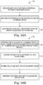
- FIGS. 10A-10B are flow diagrams illustrating one embodiment of a method for write training in a memory device.
- FIGS. 11A-11D are flow diagrams illustrating another embodiment of a method for write training in a memory device.
- FIGS. 12A-12C are flow diagrams illustrating another embodiment of a method for write training in a memory device.
- a host controller may need advanced capabilities (e.g., edge adjustments) to implement a write training sequence such that the data latched within a memory device is aligned.
- the write training sequence is performed on a single memory die at a time. Therefore, to keep the host controller complexity low, often the same setup is shared across all the memory dies of the same channel resulting in a mitigation of channel distortion only, and not mitigation of die to die variations.
- this disclosure describes embodiments for implementing write training within an integrated circuit (e.g., memory die) instead of in the host controller.
- the write training disclosed herein may be applied to several memory devices at the same time and allows an accurate edge adjustment configuration without the need for the host controller to store any information.
- the write training disclosed herein may be used to implement a fast trim-by-die procedure, thereby saving test time.
- FIG. 1 is a simplified block diagram of a first apparatus, in the form of a memory device 100 , in communication with a second apparatus, in the form of a processor 130 , as part of a third apparatus, in the form of an electronic system, according to an embodiment.
- electronic systems include personal computers, tablet computers, digital cameras, digital media players, digital recorders, games, appliances, vehicles, wireless devices, cellular telephones and the like.
- the processor 130 e.g., a controller external to the memory device 100 , may be a memory controller or other external host device.
- Memory device 100 may implement receiver write training to adjust trims used to align input data for latching within memory device 100 .
- memory device 100 may implement write training in two phases. In the first phase, using a timing alignment hardware loop, a real time sweep of a delay value used for edge adjustment may be performed during a data input burst.
- a firmware algorithm may retrieve data written to a memory (e.g., cache register) during the previous data input burst, measure DQ/DQS skew, and select internal delays to facilitate an improvement in (e.g., maximize) the data window.
- Memory device 100 includes an array of memory cells 104 logically arranged in rows and columns. Memory cells of a logical row are typically coupled to the same access line (commonly referred to as a word line) while memory cells of a logical column are typically selectively coupled to the same data line (commonly referred to as a bit line). A single access line may be associated with more than one logical row of memory cells and a single data line may be associated with more than one logical column. Memory cells (not shown in FIG. 1 ) of at least a portion of array of memory cells 104 are capable of being programmed to one of at least two data states.
- a row decode circuitry 108 and a column decode circuitry 110 are provided to decode address signals. Address signals are received and decoded to access the array of memory cells 104 .
- Memory device 100 also includes I/O control circuitry 112 to manage input of commands, addresses and data to the memory device 100 as well as output of data and status information from the memory device 100 .
- An address register 114 is in communication with I/O control circuitry 112 and row decode circuitry 108 and column decode circuitry 110 to latch the address signals prior to decoding.
- a command register 124 is in communication with I/O control circuitry 112 and control logic 116 to latch incoming commands. I/O control circuitry 112 and control logic 116 may implement the write training disclosed herein.
- An internal controller controls access to the array of memory cells 104 in response to the commands and generates status information for the external processor 130 , i.e., control logic 116 is configured to perform access operations in accordance with embodiments described herein.
- the control logic 116 is in communication with row decode circuitry 108 and column decode circuitry 110 to control the row decode circuitry 108 and column decode circuitry 110 in response to the addresses.
- Control logic 116 is also in communication with a cache register 118 .
- Cache register 118 latches data, either incoming or outgoing, as directed by control logic 116 to temporarily store data while the array of memory cells 104 is busy writing or reading, respectively, other data.
- data is passed from sensing devices 106 to the cache register 118 .
- the data is then passed from the cache register 118 to data register 120 for transfer to the array of memory cells 104 ; then new data is latched in the cache register 118 from sensing devices 106 , which receive the new data from the I/O control circuitry 112 .
- a status register 122 is in communication with I/O control circuitry 112 and control logic 116 to latch the status information for output to the processor 130 .
- Memory device 100 receives control signals at control logic 116 from processor 130 over a control link 132 .
- the control signals may include at least a chip enable CE #, a command latch enable CLE, an address latch enable ALE, a write enable WE #, and a read enable RE #. Additional control signals (not shown) may be further received over control link 132 depending upon the nature of the memory device 100 .
- Memory device 100 receives command signals (which represent commands), address signals (which represent addresses), and data signals (which represent data) from processor 130 over a multiplexed input/output (I/O) bus 134 and outputs data to processor 130 over I/O bus 134 .
- I/O input/output
- the commands are received over input/output (I/O) pins [7:0] of I/O bus 134 at I/O control circuitry 112 and are written into command register 124 .
- the addresses are received over input/output (I/O) pins [7:0] of bus 134 at I/O control circuitry 112 and are written into address register 114 .
- the data are received over input/output (I/O) pins [7:0] for an 8-bit device or input/output (I/O) pins [15:0] for a 16-bit device at I/O control circuitry 112 and are written into cache register 118 through sensing devices 106 .
- the data are subsequently written into data register 120 for programming the array of memory cells 104 .
- cache register 118 may be omitted, and the data are written directly into data register 120 through sensing devices 106 . Data are also output over input/output (I/O) pins [7:0] for an 8-bit device or input/output (I/O) pins [15:0] for a 16-bit device.
- I/O input/output
- FIG. 1 It will be appreciated by those skilled in the art that additional circuitry and signals can be provided, and that the memory device of FIG. 1 has been simplified. It should be recognized that the functionality of the various block components described with reference to FIG. 1 may not necessarily be segregated to distinct components or component portions of an integrated circuit device. For example, a single component or component portion of an integrated circuit device could be adapted to perform the functionality of more than one block component of FIG. 1 . Alternatively, one or more components or component portions of an integrated circuit device could be combined to perform the functionality of a single block component of FIG. 1 .
- I/O pins are described in accordance with popular conventions for receipt and output of the various signals, it is noted that other combinations or numbers of I/O pins may be used in the various embodiments.
- FIG. 2A is a schematic of a NAND memory array 200 A, e.g., as a portion of array of memory cells 104 .
- Memory array 200 A includes access lines, such as word lines 202 0 to 202 N , and data lines, such as bit lines 204 0 to 204 M .
- the word lines 202 may be coupled to global access lines (e.g., global word lines), not shown in FIG. 2A , in a many-to-one relationship.
- memory array 200 A may be formed over a semiconductor that, for example, may be conductively doped to have a conductivity type, such as a p-type conductivity, e.g., to form a p-well, or an n-type conductivity, e.g., to form an n-well.
- a conductivity type such as a p-type conductivity, e.g., to form a p-well, or an n-type conductivity, e.g., to form an n-well.
- Memory array 200 A might be arranged in rows (each corresponding to a word line 202 ) and columns (each corresponding to a bit line 204 ). Each column may include a string of series-coupled memory cells, such as one of NAND strings 206 0 to 206 M . Each NAND string 206 might be coupled to a common source 216 and might include memory cells 208 0 to 208 N . The memory cells 208 represent non-volatile memory cells for storage of data.
- each NAND string 206 might be connected in series between a select transistor 210 (e.g., a field-effect transistor), such as one of the select transistors 210 0 to 210 m (e.g., that may be source select transistors, commonly referred to as select gate source), and a select transistor 212 (e.g., a field-effect transistor), such as one of the select transistors 212 0 to 212 M (e.g., that may be drain select transistors, commonly referred to as select gate drain).
- a select transistor 210 e.g., a field-effect transistor
- select transistor 212 e.g., a field-effect transistor
- Select transistors 210 0 to 210 M might be commonly coupled to a select line 214 , such as a source select line, and select transistors 212 0 to 212 M might be commonly coupled to a select line 215 , such as a drain select line.
- a source of each select transistor 210 might be connected to common source 216 .
- the drain of each select transistor 210 might be connected to the source of a memory cell 208 0 of the corresponding NAND string 206 .
- the drain of select transistor 210 0 might be connected to the source of memory cell 208 0 of the corresponding NAND string 206 0 . Therefore, each select transistor 210 might be configured to selectively couple a corresponding NAND string 206 to common source 216 .
- a control gate of each select transistor 210 might be connected to select line 214 .
- each select transistor 212 might be connected to the bit line 204 for the corresponding NAND string 206 .
- the drain of select transistor 212 0 might be connected to the bit line 204 0 for the corresponding NAND string 206 0 .
- the source of each select transistor 212 might be connected to the drain of a memory cell 208 N of the corresponding NAND string 206 .
- the source of select transistor 212 0 might be connected to the drain of memory cell 208 N of the corresponding NAND string 206 0 . Therefore, each select transistor 212 might be configured to selectively couple a corresponding NAND string 206 to a corresponding bit line 204 .
- a control gate of each select transistor 212 might be connected to select line 215 .
- the memory array in FIG. 2A might be a quasi-two-dimensional memory array and might have a generally planar structure, e.g., where the common source 216 , strings 206 and bit lines 204 extend in substantially parallel planes.
- the memory array in FIG. 2A might be a three-dimensional memory array, e.g., where strings 206 may extend substantially perpendicular to a plane containing the common source 216 and to a plane containing the bit lines 204 that may be substantially parallel to the plane containing the common source 216 .
- Typical construction of memory cells 208 includes a data-storage structure 234 (e.g., a floating gate, charge trap, etc.) that can determine a data value of the cell (e.g., through changes in threshold voltage), and a control gate 236 , as shown in FIG. 2A .
- Memory cells 208 may further have a defined source 230 and a defined drain 232 .
- Memory cells 208 have their control gates 236 coupled to (and in some cases form) a word line 202 .
- a column of the memory cells 208 is a NAND string 206 or a plurality of NAND strings 206 coupled to a given bit line 204 .
- a row of the memory cells 208 are memory cells 208 commonly coupled to a given word line 202 .
- a row of memory cells 208 can, but need not include all memory cells 208 commonly coupled to a given word line 202 .
- Rows of memory cells 208 may often be divided into one or more groups of physical pages of memory cells 208 , and physical pages of memory cells 208 often include every other memory cell 208 commonly coupled to a given word line 202 .
- memory cells 208 commonly coupled to word line 202 N and selectively coupled to even bit lines 204 may be one physical page of memory cells 208 (e.g., even memory cells) while memory cells 208 commonly coupled to word line 202 N and selectively coupled to odd bit lines 204 (e.g., bit lines 204 1 , 204 3 , 204 5 , etc.) may be another physical page of memory cells 208 (e.g., odd memory cells).
- bit lines 204 3 , 204 5 are not expressly depicted in FIG.
- bit lines 204 of the array of memory cells 200 A may be numbered consecutively from bit line 204 0 to bit line 204 M .
- Other groupings of memory cells 208 commonly coupled to a given word line 202 may also define a physical page of memory cells 208 .
- all memory cells commonly coupled to a given word line might be deemed a physical page.
- the portion of a physical page (which, in some embodiments, could still be the entire row) that is read during a single read operation or programmed during a program operation (e.g., an upper or lower page memory cells) might be deemed a logical page.
- FIG. 2B is another schematic of a portion of an array of memory cells 200 B as could be used in a memory of the type described with reference to FIG. 1 , e.g., as a portion of array of memory cells 104 .
- Like numbered elements in FIG. 2B correspond to the description as provided with respect to FIG. 2A .
- FIG. 2B provides additional detail of one example of a three-dimensional NAND memory array structure.
- the three-dimensional NAND memory array 200 B may incorporate vertical structures which may include semiconductor pillars where a portion of a pillar may act as a channel region of the memory cells of NAND strings 206 .
- the NAND strings 206 may be each selectively connected to a bit line 204 0 - 204 M by a select transistor 212 (e.g., that may be drain select transistors, commonly referred to as select gate drain) and to a common source 216 by a select transistor 210 (e.g., that may be source select transistors, commonly referred to as select gate source).
- Multiple NAND strings 206 might be selectively connected to the same bit line 204 .
- Subsets of NAND strings 206 can be connected to their respective bit lines 204 by biasing the select lines 2150 - 215 L to selectively activate particular select transistors 212 each between a NAND string 206 and a bit line 204 .
- the select transistors 210 can be activated by biasing the select line 214 .
- Each word line 202 may be connected to multiple rows of memory cells of the memory array 200 B. Rows of memory cells that are commonly connected to each other by a particular word line 202 may collectively be referred to as tiers.
- FIGS. 2A and 2B are discussed in conjunction with NAND flash, the embodiments described herein are not limited to a particular array architecture or structure, and can include other structures (e.g., cross-point memory, DRAM, etc.) and other architectures (e.g., AND arrays, NOR arrays, etc.).
- other structures e.g., cross-point memory, DRAM, etc.
- other architectures e.g., AND arrays, NOR arrays, etc.
- FIG. 3 illustrates one embodiment of receiver write training 300 .
- Receiver write training 300 may receive as input a data strobe (DQS) signal on a DQS signal node 302 and a plurality of data signals DQ0 to DQ7 on a plurality of data signal nodes 304 0 to 304 7 , respectively.
- the DQ0 to DQ7 signals may include skew as shown for example for DQ7 at 308 .
- Receiver write training 300 may fix DQ-to-DQ skew on writes to a memory device.
- the memory device may measure the DQS-to-DQ timing and internally adjust DQ signal and/or DQS signal delays via trim changes as indicated by the calibration at 310 .
- the trim changes may adjust the setup time (tDS) and hold time (tDH) margins to align the DQ signals.
- tDS setup time
- tDH hold time
- the DQS signal may be aligned with each DQ0 to DQ7 signal as indicated at 312 and the data may be latched within the memory device in response to the DQS signal.
- FIG. 4 is a block diagram illustrating one embodiment of a memory device 320 for implementing receiver write training.
- Memory device 320 may include a receiver 322 with a timing alignment hardware (HW) loop, a data memory 324 , a hardware comparison circuit 326 , a firmware algorithm 332 to generate results table(s), a results table(s) memory 334 , and a firmware algorithm 336 to select trims.
- HW timing alignment hardware
- receiver 322 may receive a data pattern on I/O (e.g., DQ) nodes and a data strobe signal on a data strobe (e.g., DQS) node from a host.
- Receiver 322 may adjust delays of the received data on each I/O node while the data is received.
- Receiver 322 may latch the delayed data in response to the data strobe signal and store the latched data in data memory 324 .
- Hardware comparison logic 326 may include an XOR circuit 328 and a hardware pattern generator 330 .
- Hardware pattern generator 330 may generate an expected data pattern to match the data pattern provided by the host to the input of receiver 322 .
- hardware pattern generator 330 may be excluded and the expected data pattern may be stored in a memory (e.g., volatile memory, SRAM) of memory device 320 .
- XOR circuit 328 may compare the data pattern stored in data memory 324 to the expected data pattern to provide a comparison result.
- hardware comparison logic 326 may be excluded and the comparison of the data pattern stored in data memory 324 to the expected data pattern may be implemented in firmware logic of memory device 320 .
- firmware algorithm 332 may generate a results table or tables as will be described below with reference to FIG. 8 .
- the result table or tables are stored in the results table(s) memory (e.g., volatile memory, SRAM) 334 of memory device 320 .
- firmware algorithm 336 may select the trims (i.e., delay settings) of receiver 322 to align data received on each I/O node for latching within receiver 322 .
- FIG. 5 is a block diagram illustrating another embodiment of a memory device 400 for implementing receiver write training.
- Memory device 400 may include a plurality of input/output (I/O) nodes 402 0 to 402 I , a delay circuit 404 , a latch 406 , a memory 408 , control logic 410 , and a delay adjustment circuit 412 .
- I/O nodes 402 0 to 402 I may be communicatively coupled to the input of delay circuit 404 .
- the output of delay circuit 404 may be communicatively coupled to the input of latch 406 .
- the output of latch 406 may be communicatively coupled to the input of memory 408 .
- Memory 408 may be communicatively coupled to control logic 410 .
- Control logic 410 may be communicatively coupled to delay adjustment circuit 412 .
- Delay adjustment circuit 412 may be communicatively coupled to delay circuit 404 .
- the I/O nodes 402 0 to 402 I may receive a predefined data pattern, such as from a host.
- Delay adjustment circuit 412 may adjust a delay of delay circuit 404 for each I/O node as the predefined data pattern is received.
- delay adjustment circuit 412 may include a state machine.
- Latch 406 may latch the data received on each I/O node 402 0 to 402 I after the data is delayed by delay circuit 404 .
- Memory 408 may store the latched data.
- a deserializer (not shown) may convert serial data from the latch 406 to parallel data for storage in the memory 408 .
- Control logic 410 may compare the stored latched data to an expected data pattern and set the delay (e.g., via delay adjustment circuit 412 ) for each I/O node 402 0 to 402 I based on the comparison.
- control logic 410 may compare the stored latched data to the expected data pattern to generate a table indicating which stored latched data matches the expected data pattern and which stored latched data does not match the expected data pattern.
- control logic 410 may set the delay for each I/O node 402 0 to 402 I based on the table. After write training, data received on each I/O node 402 0 to 402 I may be aligned when latched within latch 406 .
- FIG. 6 is a block diagram illustrating another embodiment of a memory device 450 for implementing receiver write training.
- Memory device 450 may include a plurality of I/O nodes 452 0 to 452 I , a data strobe node 453 , a delay circuit 454 , a latch 456 , a cache register 458 , a controller 460 , and a state machine 462 .
- I/O nodes 452 0 to 452 I and data strobe node 453 may be communicatively coupled to the input of delay circuit 454 .
- the output of delay circuit 454 may be communicatively coupled to the input of latch 456 .
- the output of latch 456 may be communicatively coupled to the input of cache register 458 .
- Cache register 458 may be communicatively coupled to controller 460 .
- Controller 460 may be communicatively coupled to state machine 462 .
- State machine 462 may be communicatively coupled to delay circuit 454
- the I/O nodes 452 0 to 452 I may receive a periodic predefined data pattern and the data strobe node 453 may receive a data strobe signal, such as from a host.
- Delay circuit 454 may delay the data received on each I/O node 452 0 to 452 I based on a trim value for each I/O node 452 0 to 452 I .
- delay circuit 454 may also delay the data strobe signal received on data strobe node 453 based on a trim value for the data strobe node.
- Latch 456 may latch the delayed data for each I/O node 452 0 to 452 I in response to the data strobe signal.
- Cache register 458 may store the latched data.
- a deserializer (not shown) may be coupled between the latch 456 and the cache register 458 to convert serial data from the latch 456 to parallel data for storage in the cache register 458 .
- State machine 462 may change the trim value for each I/O node 452 0 to 452 I after each period of the predefined data pattern is received. In one embodiment, state machine 462 may also change the trim value for the data strobe node 453 after a plurality of periods of the predefined data pattern is received.
- Controller 460 may select the trim value for each I/O node 452 0 to 452 I based on a comparison between the stored data and an expected data pattern for each I/O node 452 0 to 452 I .
- an XOR circuit (not shown) may be used to compare the stored data to the expected data pattern for each I/O node 452 0 to 452 I .
- controller 460 may include a pattern generator to generate the expected data pattern for each I/O node 452 0 to 452 I . Controller 460 may also select the trim value for the data strobe signal based on a comparison between the stored data and the expected data pattern for each I/O node 452 0 to 452 I .
- controller 460 may select the trim value for each I/O node 452 0 to 452 I to adjust the setup and hold time margin for each I/O node 452 0 to 452 I .
- data received on each I/O node 452 0 to 452 I may be aligned when latched within latch 456 in response to the data strobe signal received on the data strobe node 453 .
- FIG. 7 is a schematic diagram illustrating one embodiment of a receiver 500 with a timing alignment hardware loop.
- receiver 500 may provide receiver 322 previously described and illustrated with reference to FIG. 4 .
- receiver 500 may provide a portion of memory device 400 (e.g., delay circuit 404 , latch 406 , delay adjustment circuit 412 ) of FIG. 5 or a portion of memory device 450 (e.g., delay circuit 454 , latch 456 , state machine 462 ) of FIG. 6 .
- Receiver 500 may include data nodes DQ[7:0] as indicated at 502 , data strobe nodes DQS/DQSN as indicated at 504 , data input buffers 506 , data strobe input buffers 508 , a delay circuit 510 , a D flip-flop (DFF) circuit 512 , a deserializer 514 , a state machine (SM) 516 , and a multiplexer 518 .
- DFF D flip-flop
- SM state machine
- Each DQ[7:0] node 502 may be electrically coupled to an input of a corresponding input buffer 506 .
- the output of each input buffer 506 may be electrically coupled to a corresponding input of delay circuit 510 .
- DQS/DQSN nodes 504 may be electrically coupled to an input of a corresponding input buffer 508 .
- the output of each input buffer 508 may be electrically coupled to a corresponding input of delay circuit 510 .
- Outputs of delay circuit 510 corresponding to each DQ[7:0] may be electrically coupled to an input of a corresponding DFF of DFF circuit 512 .
- Outputs of delay circuit 510 corresponding to DQS and DQSN may be electrically coupled to corresponding clock inputs of DFF circuit 512 .
- Outputs of DFF circuit 512 corresponding to each DQ[7:0] may be electrically coupled to corresponding inputs of deserializer 514 .
- Outputs of DFF circuit 512 corresponding to DQS and DQSN may be electrically coupled to corresponding inputs (e.g., clock inputs) of deserializer 514 .
- a clock output of deserializer 514 may be electrically coupled to an input of state machine 516 through a clock signal (ICLK_ ⁇ 4) signal path.
- a data output of deserializer 514 may be electrically coupled to a parallel data signal path (PDIO[63:0]).
- State machine 516 may be electrically coupled to a first input of multiplexer 518 through a calibration signal path and to a second input of multiplexer 518 through a receiver calibration trim signal path.
- a third input of multiplexer 518 may be electrically coupled to a factory configuration signal path.
- a host may load a periodic (e.g., 32 bytes) pre-configured data pattern on DQ[7:0] nodes 502 and the DQS and DQSN signals on DQS/DQSN nodes 504 .
- State machine 516 may set an initial trim value (via multiplexer 518 through the calibration signal path) for delay circuit 510 to delay each received DQ signal.
- Delay circuit 510 may delay each DQ signal by adjusting the DQ signal edges based on the trim value.
- the delayed DQ signals may be latched in DFF circuit 512 in response to the DQS/DQSN signals.
- Deserializer 514 may convert latched serial data from DFF circuit 512 to parallel data (i.e., PDIO[63:0]) for storage in a memory, such as data memory 324 of FIG. 4 , memory 408 of FIG. 5 , or cache register 458 of FIG. 6 .
- deserializer 514 may output every 64 bits of received data in parallel (i.e., 8 bits per DQ).
- State machine 516 may update the trim value for delay circuit 510 after each 32 bits of data is received for each DQ (i.e., after the 32 byte pre-configured data pattern is received).
- state machine 516 may update the trim value for delay circuit 510 for each period (i.e., every 32 bytes) of the pre-configured data pattern.
- the trims may be updated about every 26 ns.
- the received data for each trim value output by deserializer 514 may be saved in the memory.
- every other period of the pre-configured data pattern may be used to transition the trim value of delay circuit 510 .
- the data stored in the memory during the trim transition may be ignored since the data may be invalid.
- state machine 516 may set an initial trim value (via multiplexer 518 ) for delay circuit 510 to delay the DQS and DQSN signals.
- Delay circuit 510 may delay the DQS and DQSN signals by adjusting the DSQ and DQSN signal edges based on the trim value.
- FIG. 8 is a table 550 illustrating example pass/fail results for selecting trims in a memory device.
- table 550 may provide each results table 334 of FIG. 4 .
- Table 550 may be generated by firmware algorithm 332 of FIG. 4 , control logic 410 of FIG. 5 , or controller 460 of FIG. 6 .
- Table 550 may be generated based on the comparison of the received data stored in the memory (such as data memory 324 of FIG. 4 , memory 408 of FIG. 5 , or cache register 458 of FIG. 6 ) and the expected data.
- Table 550 include a trim 0-15 (i.e., for a predetermined number of trims equal to 16) for each column and a DQ 0-7 (i.e., for 8 DQs) for each row.
- a pass for a trim/DQ point in the table is indicated for example at 560
- a fail for a trim/DQ point in the table is indicated for example at 562 .
- a pass indicates that the received data for a DQ for the trim value matched the expected data for the DQ
- a fail indicates that the received data for a DQ for the trim value did not match the expected data for the DQ.
- One table 550 may be generated for each trim value of the data strobe signal (e.g., DQS/DQSN). Accordingly, for a predetermined number of trim values for the data strobe signal equal to 16, 16 tables 550 may be generated.
- Table 550 may be used to select the trim value for each DQ.
- table 550 may be used by firmware algorithm 336 of FIG. 4 , control logic 410 of FIG. 5 , or controller 460 of FIG. 6 to set the trim value for each DQ.
- the trim value for each DQ may be selected to maximize the setup and hold time margin for each DQ. For example, based on table 550 , trim value 5 may be selected for DQ0, trim value 7 may be selected for DQ1, trim value 6 may be selected for DQ2, trim value 9 may be selected for DQ3, trim value 7 may be selected for DQ4, trim value 6 may be selected for DQ5, trim value 8 may be selected for DQ6, and trim value 6 may be selected for DQ7.
- write training state machine 516 may set the selected trim value for each DQ via multiplexer 518 through the receiver calibration trim signal path.
- the factory configuration may be used to select the trim value for each DQ via multiplexer 518 through the factory configuration signal path.
- FIG. 9 is a block diagram illustrating one embodiment of a system 600 including a host 602 in communication with a plurality of memory (e.g., NAND) dies 604 0 to 604 J .
- Each memory die 604 0 to 604 J may include a memory device 320 of FIG. 4 , a memory device 400 of FIG. 5 , or a memory device 450 of FIG. 6 .
- host 602 may simultaneously provide a periodic predefined data pattern and a data strobe signal to each memory die 604 0 to 604 J .
- I/O nodes of each memory die 604 0 to 604 J may receive the periodic predefined data pattern and a data strobe node of each memory die 604 0 to 604 J may receive the data strobe signal.
- a delay circuit of each memory die 604 0 to 604 J may adjust a delay of data received by each I/O node based on a trim value for each I/O node and adjust a delay of the data strobe signal based on a trim value for the data strobe node.
- a latch of each memory die 604 0 to 604 J may latch the data received by each I/O node in response to the data strobe signal.
- a controller of each memory die 604 0 to 604 J may compare the latched data to an expected data pattern and set the trim value for each I/O node and the trim value for the data strobe signal based on the comparison.
- FIGS. 10A-10B are flow diagrams illustrating one embodiment of a method 700 for write training in a memory device.
- method 700 may be implemented by memory device 320 of FIG. 4 , memory device 400 of FIG. 5 , or memory device 450 of FIG. 6 .
- method 700 includes receiving input data comprising a predefined pattern at the memory device.
- method 700 includes analyzing eye openings for the received data within the memory device.
- method 700 includes adjusting setup and hold time margins within the memory device based on the analysis. In one embodiment, adjusting the setup and hold time margins of the memory device may include individually adjusting the setup and hold time margin for each I/O node of the memory device.
- Adjusting the setup and hold time margin for each I/O node of the memory device may also include aligning the latching of input data for each I/O node. Adjusting the setup and hold time margin for each I/O node of the memory device may also include individually setting a delay for each I/O node. Adjusting the setup and hold time margins of the memory device may also include adjusting an edge of a data strobe signal used to latch the input data.
- FIG. 10B illustrates one embodiment for analyzing the eye openings for the received data.
- method 700 may further include sweeping a delay value within the memory device to adjust a signal edge for each I/O node of the memory device as the predefined pattern is received.
- method 700 may further include latching the input data in response to a data strobe signal.
- method 700 may further include storing the latched input data in the memory device.
- method 700 may further include comparing the stored input data to an expected data pattern. In this embodiment, adjusting the setup and hold time margins may include setting a delay value for each I/O node based on the comparison of the stored input data to the expected data pattern.
- FIGS. 11A-11D are flow diagrams illustrating another embodiment of a method 800 for write training in a memory device.
- method 800 may be implemented by memory device 320 of FIG. 4 , memory device 400 of FIG. 5 , or memory device 450 of FIG. 6 .
- method 800 includes receiving a periodic predefined data pattern via a plurality of I/O nodes of the memory device.
- method 800 includes receiving a data strobe signal via a data strobe signal node of the memory device.
- method 800 includes latching data received by each I/O node in response to the data strobe signal.
- method 800 includes adjusting a delay for each I/O node after each period of the predefined data pattern is received.
- method 800 includes storing the latched data in the memory device.
- method 800 includes comparing the stored data for each I/O node for each period of the predefined data pattern to an expected data pattern for each I/O node.
- method 800 includes setting the delay for each I/O node based on the comparison. In one embodiment, setting the delay for each I/O node may include setting the delay for each I/O node to align the latching of data received by each I/O node.
- method 800 may further include generating a table indicating which stored data for each I/O node for each period of the predefined data pattern matches the expected data pattern for each I/O node and which stored data for each I/O node for each period of the predefined data pattern does not match the expected data pattern for each I/O node.
- setting the delay for each I/O node may include setting the delay for each I/O node based on the table indicating which stored data for each I/O node for each period of the predefined data pattern matches the expected data pattern for each I/O node.
- method 800 may further include storing the table in a volatile memory of the memory device.
- method 800 may further include adjusting a delay for the data strobe signal after a plurality of periods of the predefined data pattern is received.
- method 800 may further include setting the delay of the data strobe signal based on the comparison to maximize setup and hold time margins for data received by each I/O node.
- FIGS. 12A-12C are flow diagrams illustrating another embodiment of a method 900 for write training in a memory device.
- method 900 may be implemented by system 600 of FIG. 9 .
- method 900 includes loading, via a host, a periodic predefined data pattern to a plurality of I/O nodes of a first memory die.
- the plurality of I/O nodes may equal 8 I/O nodes, and the periodic predefined data pattern may repeat every 32 bytes.
- method 900 includes changing, within the first memory die, a trim value of a delay for each I/O node of the first memory die after each period of the predefined data pattern.
- changing, within the first memory die, the trim value may include incrementing the trim value after each period of the predefined data pattern with the trim value starting at 0 and ending at a predetermined trim value.
- method 900 includes latching, within the first memory die, the delayed data for each I/O node of the first memory die.
- method 900 includes comparing, within the first memory die, the latched data for each I/O node of the first memory die to an expected data pattern.
- method 900 includes setting, within the first memory die, the trim value of the delay for each I/O node of the first memory die based on the comparison.
- method 900 may further include loading, via the host and simultaneously with loading the periodic predefined data pattern to the plurality of I/O nodes of the first memory die, the periodic predefined data pattern to a plurality of I/O nodes of a second memory die.
- method 900 may further include changing, within the second memory die, a trim value of a delay for each I/O node of the second memory die after each period of the predefined data pattern.
- method 900 may further include latching, within the second memory die, the delayed data for each I/O node of the second memory die.
- method 900 may further include comparing, within the second memory die, the latched data for each I/O node of the second memory die to an expected data pattern.
- method 900 may further include setting, within the second memory die, the trim value of the delay for each I/O node of the second memory die based on the comparison.
- method 900 may further include providing, via the host, a data strobe signal to a data strobe node of the first memory die.
- method 900 may further include changing, within the first memory die, a trim value of a delay for the data strobe signal of the first memory die after a plurality of periods of the predefined data pattern.
- method 900 may further include latching, within the first memory die, the delayed data for each I/O node of the first memory die in response to the data strobe signal of the first memory die.
- method 900 may further include setting, within the first memory die, the trim value of the delay for the data strobe signal of the first memory die based on the comparison.
Landscapes
- Engineering & Computer Science (AREA)
- Theoretical Computer Science (AREA)
- Human Computer Interaction (AREA)
- Physics & Mathematics (AREA)
- General Engineering & Computer Science (AREA)
- General Physics & Mathematics (AREA)
- Microelectronics & Electronic Packaging (AREA)
- Memory System (AREA)
- Dram (AREA)
- Techniques For Improving Reliability Of Storages (AREA)
Abstract
Description
Claims (19)
Priority Applications (8)
| Application Number | Priority Date | Filing Date | Title |
|---|---|---|---|
| US16/171,442 US11079946B2 (en) | 2018-10-26 | 2018-10-26 | Write training in memory devices |
| KR1020217011930A KR20210048577A (en) | 2018-10-26 | 2019-09-18 | Write training on memory devices |
| CN201980069819.4A CN112912956B (en) | 2018-10-26 | 2019-09-18 | Write training in memory devices |
| EP19876800.4A EP3871220A4 (en) | 2018-10-26 | 2019-09-18 | Write training in memory devices |
| PCT/US2019/051625 WO2020086195A1 (en) | 2018-10-26 | 2019-09-18 | Write training in memory devices |
| TW108135012A TWI725561B (en) | 2018-10-26 | 2019-09-27 | Write training in memory devices |
| US17/316,956 US11733887B2 (en) | 2018-10-26 | 2021-05-11 | Write training in memory devices by adjusting delays based on data patterns |
| US18/351,429 US20240012573A1 (en) | 2018-10-26 | 2023-07-12 | Write training in memory devices |
Applications Claiming Priority (1)
| Application Number | Priority Date | Filing Date | Title |
|---|---|---|---|
| US16/171,442 US11079946B2 (en) | 2018-10-26 | 2018-10-26 | Write training in memory devices |
Related Child Applications (1)
| Application Number | Title | Priority Date | Filing Date |
|---|---|---|---|
| US17/316,956 Division US11733887B2 (en) | 2018-10-26 | 2021-05-11 | Write training in memory devices by adjusting delays based on data patterns |
Publications (2)
| Publication Number | Publication Date |
|---|---|
| US20200133540A1 US20200133540A1 (en) | 2020-04-30 |
| US11079946B2 true US11079946B2 (en) | 2021-08-03 |
Family
ID=70328658
Family Applications (3)
| Application Number | Title | Priority Date | Filing Date |
|---|---|---|---|
| US16/171,442 Active 2039-04-25 US11079946B2 (en) | 2018-10-26 | 2018-10-26 | Write training in memory devices |
| US17/316,956 Active 2038-12-17 US11733887B2 (en) | 2018-10-26 | 2021-05-11 | Write training in memory devices by adjusting delays based on data patterns |
| US18/351,429 Pending US20240012573A1 (en) | 2018-10-26 | 2023-07-12 | Write training in memory devices |
Family Applications After (2)
| Application Number | Title | Priority Date | Filing Date |
|---|---|---|---|
| US17/316,956 Active 2038-12-17 US11733887B2 (en) | 2018-10-26 | 2021-05-11 | Write training in memory devices by adjusting delays based on data patterns |
| US18/351,429 Pending US20240012573A1 (en) | 2018-10-26 | 2023-07-12 | Write training in memory devices |
Country Status (6)
| Country | Link |
|---|---|
| US (3) | US11079946B2 (en) |
| EP (1) | EP3871220A4 (en) |
| KR (1) | KR20210048577A (en) |
| CN (1) | CN112912956B (en) |
| TW (1) | TWI725561B (en) |
| WO (1) | WO2020086195A1 (en) |
Families Citing this family (13)
| Publication number | Priority date | Publication date | Assignee | Title |
|---|---|---|---|---|
| US11450613B2 (en) * | 2018-03-23 | 2022-09-20 | Intel Corporation | Integrated circuit package with test circuitry for testing a channel between dies |
| KR20200126666A (en) | 2019-04-30 | 2020-11-09 | 에스케이하이닉스 주식회사 | Memory system and operating method thereof |
| KR20200137548A (en) | 2019-05-30 | 2020-12-09 | 에스케이하이닉스 주식회사 | Memory device and test operating method thereof |
| KR20200126678A (en) * | 2019-04-30 | 2020-11-09 | 에스케이하이닉스 주식회사 | Memory system and operating method thereof |
| KR20200124045A (en) | 2019-04-23 | 2020-11-02 | 에스케이하이닉스 주식회사 | Memory system and operating method thereof |
| US11404097B2 (en) | 2018-12-11 | 2022-08-02 | SK Hynix Inc. | Memory system and operating method of the memory system |
| US11139010B2 (en) | 2018-12-11 | 2021-10-05 | SK Hynix Inc. | Memory system and operating method of the memory system |
| US11309013B2 (en) | 2020-04-29 | 2022-04-19 | Samsung Electronics Co., Ltd. | Memory device for reducing resources used for training |
| US11081193B1 (en) | 2020-06-16 | 2021-08-03 | Sandisk Technologies Llc | Inverter based delay chain for calibrating data signal to a clock |
| US11829281B2 (en) * | 2021-06-16 | 2023-11-28 | Sandisk Technologies Llc | Semi receiver side write training for non-volatile memory system |
| US12424264B2 (en) | 2023-03-14 | 2025-09-23 | Powerchip Semiconductor Manufacturing Corporation | Stacked memory with a timing adjustment function |
| KR20250154066A (en) * | 2024-04-19 | 2025-10-28 | 에스케이하이닉스 주식회사 | Write training circuit, semiconductor memory apparatus and data processing system including the write training circuit |
| KR20250165846A (en) * | 2024-05-20 | 2025-11-27 | 삼성전자주식회사 | Memory apparatus and operation method thereof |
Citations (32)
| Publication number | Priority date | Publication date | Assignee | Title |
|---|---|---|---|---|
| TW495966B (en) | 2000-06-20 | 2002-07-21 | Mitsubishi Electric Corp | Semiconductor integrated circuit device allowing accurate evaluation of access time of memory contained therein and access time evaluating method |
| US20030167417A1 (en) * | 2002-03-01 | 2003-09-04 | To Hing Y. | Method and apparatus for capturing data from a memory subsystem |
| US6691214B1 (en) * | 2000-08-29 | 2004-02-10 | Micron Technology, Inc. | DDR II write data capture calibration |
| US6735709B1 (en) * | 2000-11-09 | 2004-05-11 | Micron Technology, Inc. | Method of timing calibration using slower data rate pattern |
| US6763444B2 (en) * | 2001-05-08 | 2004-07-13 | Micron Technology, Inc. | Read/write timing calibration of a memory array using a row or a redundant row |
| TW200525349A (en) | 2003-10-16 | 2005-08-01 | Intel Corp | Adaptive input/output buffer and methods thereof |
| US20060268632A1 (en) * | 2005-05-25 | 2006-11-30 | Josef Schnell | Integrated circuit chip having a first delay circuit trimmed via a second delay circuit |
| US7167966B2 (en) | 2001-09-29 | 2007-01-23 | Apple Computer, Inc. | Method and apparatus for a calibrated variable phase offset timing between synchronous clock subdomains |
| WO2007106766A2 (en) | 2006-03-16 | 2007-09-20 | Rambus Inc. | Signaling system with adaptive timing calibration |
| US20090310433A1 (en) * | 2008-06-12 | 2009-12-17 | Honeywell Internationa Inc. | Data alignment and de-skew system and method for double data rate input data stream |
| US20100180143A1 (en) * | 2007-04-19 | 2010-07-15 | Rambus Inc. | Techniques for improved timing control of memory devices |
| TW201104682A (en) | 2009-07-27 | 2011-02-01 | Sunplus Technology Co Ltd | Apparatus and method for data strobe and timing variation detection of an SDRAM interface |
| US7983094B1 (en) | 2006-11-06 | 2011-07-19 | Altera Corporation | PVT compensated auto-calibration scheme for DDR3 |
| US20120051161A1 (en) * | 2010-08-31 | 2012-03-01 | Micron Technology, Inc. | Memory devices and methods of operating memory |
| US20120087194A1 (en) * | 2010-10-11 | 2012-04-12 | Tae-Young Oh | Data write training method and semiconductor device performing the same |
| TW201415480A (en) | 2012-10-15 | 2014-04-16 | Via Tech Inc | Data storage device, and storage media controller and control method |
| US20140177377A1 (en) * | 2012-12-24 | 2014-06-26 | Arm Limited | Data signal receiver and method of calibrating a data signal receiver |
| CN104134454A (en) | 2007-12-21 | 2014-11-05 | 拉姆伯斯公司 | Method and apparatus for calibrating write timing in a memory system |
| US20150181905A1 (en) * | 2013-12-27 | 2015-07-02 | Tsuji Oil Mills Co., Ltd. | Lecithin or lecithin preparation having resistance to heat discoloration and a method for producing the same |
| US20150248925A1 (en) | 2014-02-28 | 2015-09-03 | Texas Instruments Incorporated | On chip characterization of timing parameters for memory ports |
| US9275706B2 (en) * | 2013-02-28 | 2016-03-01 | Sandisk Technologies Inc. | Auto-calibration for high speed input/output |
| US20160096854A1 (en) * | 2014-10-07 | 2016-04-07 | Tsuji Oil Mills Co., Ltd. | Method for suppressing heat discoloration of lecithin |
| US9312022B1 (en) * | 2015-01-06 | 2016-04-12 | Micron Technology, Inc. | Memory timing self-calibration |
| US20160314822A1 (en) * | 2015-03-16 | 2016-10-27 | Rambus Inc. | Training and operations with a double buffered memory topology |
| US9530473B2 (en) | 2014-05-22 | 2016-12-27 | Micron Technology, Inc. | Apparatuses and methods for timing provision of a command to input circuitry |
| US9865317B2 (en) | 2016-04-26 | 2018-01-09 | Micron Technology, Inc. | Methods and apparatuses including command delay adjustment circuit |
| US20200187521A1 (en) * | 2018-12-17 | 2020-06-18 | Warouj KACHICHIAN | Food Composition and Methods of Making and Using the Same |
| US20200190449A1 (en) * | 2017-08-22 | 2020-06-18 | Euphoria Research And Development Ltd. | Enriched alcoholic beverages |
| US10689682B2 (en) * | 2014-10-17 | 2020-06-23 | Suntory Holdings Limited | Mogrol glycosyltransferase and gene encoding same |
| US10688210B2 (en) * | 2012-08-28 | 2020-06-23 | Sensor Electronic Technology, Inc. | Storage device including ultraviolet illumination |
| US20200198883A1 (en) * | 2018-12-19 | 2020-06-25 | Ricardo Haces Menéndez | Kit for a confectionery product and a method related thereof |
| US20200197465A1 (en) * | 2017-05-23 | 2020-06-25 | Luke Klele | Natural product compositions for treating or managing symptoms of add, adhd, anxiety, and depression |
Family Cites Families (8)
| Publication number | Priority date | Publication date | Assignee | Title |
|---|---|---|---|---|
| JP4119581B2 (en) * | 1999-09-02 | 2008-07-16 | 富士通株式会社 | Data transmission device, data output device, and data transmission method |
| US7855931B2 (en) * | 2008-07-21 | 2010-12-21 | Micron Technology, Inc. | Memory system and method using stacked memory device dice, and system using the memory system |
| JP2010086246A (en) * | 2008-09-30 | 2010-04-15 | Nec Electronics Corp | Memory interface and operation method for the memory interface |
| US20120110400A1 (en) | 2010-11-01 | 2012-05-03 | Altera Corporation | Method and Apparatus for Performing Memory Interface Calibration |
| US9355696B1 (en) * | 2014-11-06 | 2016-05-31 | Xilinx, Inc. | Calibration in a control device receiving from a source synchronous interface |
| US9886987B1 (en) * | 2014-12-30 | 2018-02-06 | Cadence Design System, Inc. | System and method for data-mask training in non-provisioned random access memory |
| KR20180034738A (en) * | 2016-09-26 | 2018-04-05 | 삼성전자주식회사 | Memory device and divided clock compensation method thereof |
| US11424753B2 (en) * | 2020-11-06 | 2022-08-23 | Ay Dee Kay Llc | Successive-approximation-register (SAR) analog-to-digital converter (ADC) timing calibration |
-
2018
- 2018-10-26 US US16/171,442 patent/US11079946B2/en active Active
-
2019
- 2019-09-18 WO PCT/US2019/051625 patent/WO2020086195A1/en not_active Ceased
- 2019-09-18 CN CN201980069819.4A patent/CN112912956B/en active Active
- 2019-09-18 EP EP19876800.4A patent/EP3871220A4/en active Pending
- 2019-09-18 KR KR1020217011930A patent/KR20210048577A/en not_active Ceased
- 2019-09-27 TW TW108135012A patent/TWI725561B/en active
-
2021
- 2021-05-11 US US17/316,956 patent/US11733887B2/en active Active
-
2023
- 2023-07-12 US US18/351,429 patent/US20240012573A1/en active Pending
Patent Citations (33)
| Publication number | Priority date | Publication date | Assignee | Title |
|---|---|---|---|---|
| TW495966B (en) | 2000-06-20 | 2002-07-21 | Mitsubishi Electric Corp | Semiconductor integrated circuit device allowing accurate evaluation of access time of memory contained therein and access time evaluating method |
| US6691214B1 (en) * | 2000-08-29 | 2004-02-10 | Micron Technology, Inc. | DDR II write data capture calibration |
| US6735709B1 (en) * | 2000-11-09 | 2004-05-11 | Micron Technology, Inc. | Method of timing calibration using slower data rate pattern |
| US6763444B2 (en) * | 2001-05-08 | 2004-07-13 | Micron Technology, Inc. | Read/write timing calibration of a memory array using a row or a redundant row |
| US7167966B2 (en) | 2001-09-29 | 2007-01-23 | Apple Computer, Inc. | Method and apparatus for a calibrated variable phase offset timing between synchronous clock subdomains |
| US20030167417A1 (en) * | 2002-03-01 | 2003-09-04 | To Hing Y. | Method and apparatus for capturing data from a memory subsystem |
| TW200525349A (en) | 2003-10-16 | 2005-08-01 | Intel Corp | Adaptive input/output buffer and methods thereof |
| US20060268632A1 (en) * | 2005-05-25 | 2006-11-30 | Josef Schnell | Integrated circuit chip having a first delay circuit trimmed via a second delay circuit |
| WO2007106766A2 (en) | 2006-03-16 | 2007-09-20 | Rambus Inc. | Signaling system with adaptive timing calibration |
| WO2007106766A3 (en) | 2006-03-16 | 2008-01-31 | Rambus Inc | Signaling system with adaptive timing calibration |
| US7983094B1 (en) | 2006-11-06 | 2011-07-19 | Altera Corporation | PVT compensated auto-calibration scheme for DDR3 |
| US20100180143A1 (en) * | 2007-04-19 | 2010-07-15 | Rambus Inc. | Techniques for improved timing control of memory devices |
| CN104134454A (en) | 2007-12-21 | 2014-11-05 | 拉姆伯斯公司 | Method and apparatus for calibrating write timing in a memory system |
| US20090310433A1 (en) * | 2008-06-12 | 2009-12-17 | Honeywell Internationa Inc. | Data alignment and de-skew system and method for double data rate input data stream |
| TW201104682A (en) | 2009-07-27 | 2011-02-01 | Sunplus Technology Co Ltd | Apparatus and method for data strobe and timing variation detection of an SDRAM interface |
| US20120051161A1 (en) * | 2010-08-31 | 2012-03-01 | Micron Technology, Inc. | Memory devices and methods of operating memory |
| US20120087194A1 (en) * | 2010-10-11 | 2012-04-12 | Tae-Young Oh | Data write training method and semiconductor device performing the same |
| US10688210B2 (en) * | 2012-08-28 | 2020-06-23 | Sensor Electronic Technology, Inc. | Storage device including ultraviolet illumination |
| TW201415480A (en) | 2012-10-15 | 2014-04-16 | Via Tech Inc | Data storage device, and storage media controller and control method |
| US20140177377A1 (en) * | 2012-12-24 | 2014-06-26 | Arm Limited | Data signal receiver and method of calibrating a data signal receiver |
| US9275706B2 (en) * | 2013-02-28 | 2016-03-01 | Sandisk Technologies Inc. | Auto-calibration for high speed input/output |
| US20150181905A1 (en) * | 2013-12-27 | 2015-07-02 | Tsuji Oil Mills Co., Ltd. | Lecithin or lecithin preparation having resistance to heat discoloration and a method for producing the same |
| US20150248925A1 (en) | 2014-02-28 | 2015-09-03 | Texas Instruments Incorporated | On chip characterization of timing parameters for memory ports |
| US9530473B2 (en) | 2014-05-22 | 2016-12-27 | Micron Technology, Inc. | Apparatuses and methods for timing provision of a command to input circuitry |
| US20160096854A1 (en) * | 2014-10-07 | 2016-04-07 | Tsuji Oil Mills Co., Ltd. | Method for suppressing heat discoloration of lecithin |
| US10689682B2 (en) * | 2014-10-17 | 2020-06-23 | Suntory Holdings Limited | Mogrol glycosyltransferase and gene encoding same |
| US9312022B1 (en) * | 2015-01-06 | 2016-04-12 | Micron Technology, Inc. | Memory timing self-calibration |
| US20160314822A1 (en) * | 2015-03-16 | 2016-10-27 | Rambus Inc. | Training and operations with a double buffered memory topology |
| US9865317B2 (en) | 2016-04-26 | 2018-01-09 | Micron Technology, Inc. | Methods and apparatuses including command delay adjustment circuit |
| US20200197465A1 (en) * | 2017-05-23 | 2020-06-25 | Luke Klele | Natural product compositions for treating or managing symptoms of add, adhd, anxiety, and depression |
| US20200190449A1 (en) * | 2017-08-22 | 2020-06-18 | Euphoria Research And Development Ltd. | Enriched alcoholic beverages |
| US20200187521A1 (en) * | 2018-12-17 | 2020-06-18 | Warouj KACHICHIAN | Food Composition and Methods of Making and Using the Same |
| US20200198883A1 (en) * | 2018-12-19 | 2020-06-25 | Ricardo Haces Menéndez | Kit for a confectionery product and a method related thereof |
Non-Patent Citations (1)
| Title |
|---|
| International Search Report and Written Opinion of the International Searching Authority for Application No. PCT/US2019/051625 dated Jan. 3, 2020 (13 pages). |
Also Published As
| Publication number | Publication date |
|---|---|
| TW202020867A (en) | 2020-06-01 |
| EP3871220A4 (en) | 2022-07-13 |
| KR20210048577A (en) | 2021-05-03 |
| CN112912956B (en) | 2024-05-10 |
| US20240012573A1 (en) | 2024-01-11 |
| US20210263660A1 (en) | 2021-08-26 |
| CN112912956A (en) | 2021-06-04 |
| WO2020086195A1 (en) | 2020-04-30 |
| US20200133540A1 (en) | 2020-04-30 |
| US11733887B2 (en) | 2023-08-22 |
| EP3871220A1 (en) | 2021-09-01 |
| TWI725561B (en) | 2021-04-21 |
Similar Documents
| Publication | Publication Date | Title |
|---|---|---|
| US11733887B2 (en) | Write training in memory devices by adjusting delays based on data patterns | |
| US9460803B1 (en) | Data path with clock-data tracking | |
| US11710523B2 (en) | Apparatus for discharging control gates after performing a sensing operation on a memory cell | |
| US11367473B2 (en) | Wave pipeline | |
| US10366767B2 (en) | Memory devices configured to perform leak checks | |
| US10950316B2 (en) | Apparatus for determining a pass voltage of a read operation | |
| US20220084610A1 (en) | Apparatus for mitigating program disturb | |
| US9552857B1 (en) | Address generation circuit and semiconductor memory device including the same | |
| US10714160B2 (en) | Wave pipeline | |
| US10885987B2 (en) | Reading even data lines or odd data lines coupled to memory cell strings | |
| US11125819B2 (en) | Comparator | |
| US11544208B2 (en) | Wave pipeline including synchronous stage | |
| US11231853B2 (en) | Memory including search logic |
Legal Events
| Date | Code | Title | Description |
|---|---|---|---|
| AS | Assignment |
Owner name: MICRON TECHNOLOGY, INC., IDAHO Free format text: ASSIGNMENT OF ASSIGNORS INTEREST;ASSIGNORS:PILOLLI, LUIGI;FEIZ ZARRIN GHALAM, ALI;WANG, GUAN;AND OTHERS;SIGNING DATES FROM 20181011 TO 20181025;REEL/FRAME:047323/0237 |
|
| FEPP | Fee payment procedure |
Free format text: ENTITY STATUS SET TO UNDISCOUNTED (ORIGINAL EVENT CODE: BIG.); ENTITY STATUS OF PATENT OWNER: LARGE ENTITY |
|
| STPP | Information on status: patent application and granting procedure in general |
Free format text: DOCKETED NEW CASE - READY FOR EXAMINATION |
|
| AS | Assignment |
Owner name: MORGAN STANLEY SENIOR FUNDING, INC., AS COLLATERAL AGENT, MARYLAND Free format text: SUPPLEMENT NO. 12 TO PATENT SECURITY AGREEMENT;ASSIGNOR:MICRON TECHNOLOGY, INC.;REEL/FRAME:048948/0677 Effective date: 20190416 Owner name: JPMORGAN CHASE BANK, N.A., AS COLLATERAL AGENT, ILLINOIS Free format text: SUPPLEMENT NO. 3 TO PATENT SECURITY AGREEMENT;ASSIGNOR:MICRON TECHNOLOGY, INC.;REEL/FRAME:048951/0902 Effective date: 20190416 |
|
| AS | Assignment |
Owner name: MICRON TECHNOLOGY, INC., IDAHO Free format text: RELEASE BY SECURED PARTY;ASSIGNOR:MORGAN STANLEY SENIOR FUNDING, INC., AS COLLATERAL AGENT;REEL/FRAME:050724/0392 Effective date: 20190731 |
|
| AS | Assignment |
Owner name: MICRON TECHNOLOGY, INC., IDAHO Free format text: RELEASE BY SECURED PARTY;ASSIGNOR:JPMORGAN CHASE BANK, N.A., AS COLLATERAL AGENT;REEL/FRAME:051041/0317 Effective date: 20190731 |
|
| STPP | Information on status: patent application and granting procedure in general |
Free format text: RESPONSE TO NON-FINAL OFFICE ACTION ENTERED AND FORWARDED TO EXAMINER |
|
| STPP | Information on status: patent application and granting procedure in general |
Free format text: NON FINAL ACTION MAILED |
|
| STPP | Information on status: patent application and granting procedure in general |
Free format text: RESPONSE TO NON-FINAL OFFICE ACTION ENTERED AND FORWARDED TO EXAMINER |
|
| STPP | Information on status: patent application and granting procedure in general |
Free format text: NOTICE OF ALLOWANCE MAILED -- APPLICATION RECEIVED IN OFFICE OF PUBLICATIONS |
|
| STPP | Information on status: patent application and granting procedure in general |
Free format text: AWAITING TC RESP., ISSUE FEE NOT PAID |
|
| STPP | Information on status: patent application and granting procedure in general |
Free format text: NOTICE OF ALLOWANCE MAILED -- APPLICATION RECEIVED IN OFFICE OF PUBLICATIONS |
|
| STPP | Information on status: patent application and granting procedure in general |
Free format text: PUBLICATIONS -- ISSUE FEE PAYMENT RECEIVED |
|
| STPP | Information on status: patent application and granting procedure in general |
Free format text: PUBLICATIONS -- ISSUE FEE PAYMENT VERIFIED |
|
| STCF | Information on status: patent grant |
Free format text: PATENTED CASE |
|
| AS | Assignment |
Owner name: LODESTAR LICENSING GROUP LLC, ILLINOIS Free format text: CONFIRMATORY LICENSE;ASSIGNOR:MICRON TECHNOLOGY, INC.;REEL/FRAME:065312/0505 Effective date: 20230323 |
|
| MAFP | Maintenance fee payment |
Free format text: PAYMENT OF MAINTENANCE FEE, 4TH YEAR, LARGE ENTITY (ORIGINAL EVENT CODE: M1551); ENTITY STATUS OF PATENT OWNER: LARGE ENTITY Year of fee payment: 4 |