US11079446B2 - Compact sensor package - Google Patents
Compact sensor package Download PDFInfo
- Publication number
- US11079446B2 US11079446B2 US15/497,296 US201715497296A US11079446B2 US 11079446 B2 US11079446 B2 US 11079446B2 US 201715497296 A US201715497296 A US 201715497296A US 11079446 B2 US11079446 B2 US 11079446B2
- Authority
- US
- United States
- Prior art keywords
- magnetic
- magnetic sensor
- component board
- magnetic field
- sensor package
- Prior art date
- Legal status (The legal status is an assumption and is not a legal conclusion. Google has not performed a legal analysis and makes no representation as to the accuracy of the status listed.)
- Active, expires
Links
- 230000004308 accommodation Effects 0.000 claims abstract description 46
- 239000004065 semiconductor Substances 0.000 claims description 16
- 239000008393 encapsulating agent Substances 0.000 description 23
- 239000004020 conductor Substances 0.000 description 11
- 238000001514 detection method Methods 0.000 description 10
- 238000000034 method Methods 0.000 description 8
- 230000008901 benefit Effects 0.000 description 5
- 238000004519 manufacturing process Methods 0.000 description 5
- 239000000758 substrate Substances 0.000 description 5
- CWYNVVGOOAEACU-UHFFFAOYSA-N Fe2+ Chemical compound [Fe+2] CWYNVVGOOAEACU-UHFFFAOYSA-N 0.000 description 4
- 150000001875 compounds Chemical class 0.000 description 3
- 230000005355 Hall effect Effects 0.000 description 2
- XUIMIQQOPSSXEZ-UHFFFAOYSA-N Silicon Chemical compound [Si] XUIMIQQOPSSXEZ-UHFFFAOYSA-N 0.000 description 2
- 238000005452 bending Methods 0.000 description 2
- 230000009286 beneficial effect Effects 0.000 description 2
- 239000000969 carrier Substances 0.000 description 2
- 238000010276 construction Methods 0.000 description 2
- 238000005530 etching Methods 0.000 description 2
- 239000000463 material Substances 0.000 description 2
- 238000005259 measurement Methods 0.000 description 2
- 239000000203 mixture Substances 0.000 description 2
- 229910052710 silicon Inorganic materials 0.000 description 2
- 239000010703 silicon Substances 0.000 description 2
- 229910000831 Steel Inorganic materials 0.000 description 1
- 230000015556 catabolic process Effects 0.000 description 1
- 230000003750 conditioning effect Effects 0.000 description 1
- 238000006073 displacement reaction Methods 0.000 description 1
- 230000009977 dual effect Effects 0.000 description 1
- 238000003780 insertion Methods 0.000 description 1
- 230000037431 insertion Effects 0.000 description 1
- 238000002955 isolation Methods 0.000 description 1
- 239000000696 magnetic material Substances 0.000 description 1
- 230000005415 magnetization Effects 0.000 description 1
- 230000007257 malfunction Effects 0.000 description 1
- 239000011159 matrix material Substances 0.000 description 1
- 229910000679 solder Inorganic materials 0.000 description 1
- 239000010959 steel Substances 0.000 description 1
- 239000002699 waste material Substances 0.000 description 1
Images


Classifications
-
- G—PHYSICS
- G01—MEASURING; TESTING
- G01R—MEASURING ELECTRIC VARIABLES; MEASURING MAGNETIC VARIABLES
- G01R33/00—Arrangements or instruments for measuring magnetic variables
- G01R33/0005—Geometrical arrangement of magnetic sensor elements; Apparatus combining different magnetic sensor types
-
- G—PHYSICS
- G01—MEASURING; TESTING
- G01R—MEASURING ELECTRIC VARIABLES; MEASURING MAGNETIC VARIABLES
- G01R33/00—Arrangements or instruments for measuring magnetic variables
- G01R33/0052—Manufacturing aspects; Manufacturing of single devices, i.e. of semiconductor magnetic sensor chips
-
- G—PHYSICS
- G01—MEASURING; TESTING
- G01D—MEASURING NOT SPECIALLY ADAPTED FOR A SPECIFIC VARIABLE; ARRANGEMENTS FOR MEASURING TWO OR MORE VARIABLES NOT COVERED IN A SINGLE OTHER SUBCLASS; TARIFF METERING APPARATUS; MEASURING OR TESTING NOT OTHERWISE PROVIDED FOR
- G01D5/00—Mechanical means for transferring the output of a sensing member; Means for converting the output of a sensing member to another variable where the form or nature of the sensing member does not constrain the means for converting; Transducers not specially adapted for a specific variable
- G01D5/12—Mechanical means for transferring the output of a sensing member; Means for converting the output of a sensing member to another variable where the form or nature of the sensing member does not constrain the means for converting; Transducers not specially adapted for a specific variable using electric or magnetic means
- G01D5/14—Mechanical means for transferring the output of a sensing member; Means for converting the output of a sensing member to another variable where the form or nature of the sensing member does not constrain the means for converting; Transducers not specially adapted for a specific variable using electric or magnetic means influencing the magnitude of a current or voltage
- G01D5/142—Mechanical means for transferring the output of a sensing member; Means for converting the output of a sensing member to another variable where the form or nature of the sensing member does not constrain the means for converting; Transducers not specially adapted for a specific variable using electric or magnetic means influencing the magnitude of a current or voltage using Hall-effect devices
- G01D5/147—Mechanical means for transferring the output of a sensing member; Means for converting the output of a sensing member to another variable where the form or nature of the sensing member does not constrain the means for converting; Transducers not specially adapted for a specific variable using electric or magnetic means influencing the magnitude of a current or voltage using Hall-effect devices influenced by the movement of a third element, the position of Hall device and the source of magnetic field being fixed in respect to each other
-
- G—PHYSICS
- G01—MEASURING; TESTING
- G01R—MEASURING ELECTRIC VARIABLES; MEASURING MAGNETIC VARIABLES
- G01R15/00—Details of measuring arrangements of the types provided for in groups G01R17/00 - G01R29/00, G01R33/00 - G01R33/26 or G01R35/00
- G01R15/14—Adaptations providing voltage or current isolation, e.g. for high-voltage or high-current networks
- G01R15/20—Adaptations providing voltage or current isolation, e.g. for high-voltage or high-current networks using galvano-magnetic devices, e.g. Hall-effect devices, i.e. measuring a magnetic field via the interaction between a current and a magnetic field, e.g. magneto resistive or Hall effect devices
-
- G—PHYSICS
- G01—MEASURING; TESTING
- G01R—MEASURING ELECTRIC VARIABLES; MEASURING MAGNETIC VARIABLES
- G01R19/00—Arrangements for measuring currents or voltages or for indicating presence or sign thereof
- G01R19/0092—Arrangements for measuring currents or voltages or for indicating presence or sign thereof measuring current only
-
- G—PHYSICS
- G01—MEASURING; TESTING
- G01R—MEASURING ELECTRIC VARIABLES; MEASURING MAGNETIC VARIABLES
- G01R33/00—Arrangements or instruments for measuring magnetic variables
- G01R33/02—Measuring direction or magnitude of magnetic fields or magnetic flux
- G01R33/06—Measuring direction or magnitude of magnetic fields or magnetic flux using galvano-magnetic devices
- G01R33/07—Hall effect devices
-
- G—PHYSICS
- G01—MEASURING; TESTING
- G01R—MEASURING ELECTRIC VARIABLES; MEASURING MAGNETIC VARIABLES
- G01R33/00—Arrangements or instruments for measuring magnetic variables
- G01R33/02—Measuring direction or magnitude of magnetic fields or magnetic flux
- G01R33/06—Measuring direction or magnitude of magnetic fields or magnetic flux using galvano-magnetic devices
- G01R33/09—Magnetoresistive devices
- G01R33/091—Constructional adaptation of the sensor to specific applications
Definitions
- the present invention relates to magnetic sensor arrangements, and to methods of manufacturing a magnetic sensor arrangement.
- Conventional magnetic sensor arrangements comprise two magnetic parts mounted on a shaft and spaced apart along a rotation axis of the shaft.
- a magnetic field sensor element may be placed in between both parts.
- Such types of magnetic parts are useful to generate magnetic fields with high symmetry.
- the mentioned arrangement may be operated as angle sensor. A proper angle accuracy may be obtained in spite of assembly tolerances of all components.
- a magnetic sensor arrangement which comprises a component board delimited by two opposing main surfaces and having an accommodation hole (wherein the hole may for instance be a through hole, an aperture, or a recess of the component board) for accommodating at least part of a magnetic field generating structure, and a magnetic sensor package located at least partially between the two opposing main surfaces and configured for sensing a magnetic field generated by the magnetic field generating structure.
- a magnetic sensor arrangement which comprises a component board having an accommodation hole (wherein the hole may for instance be a through hole, an aperture, or a recess of the component board) for accommodating at least part of a magnetic field generating structure, and a magnetic sensor package mounted on and/or in the component board and configured for sensing a magnetic field generated by the magnetic field generating structure, wherein the magnetic sensor package comprises a sensing element on a carrier, and wherein the sensing element extends from the carrier towards the component board.
- a method of manufacturing a magnetic sensor arrangement comprises providing a component board delimited by two opposing main surfaces with an accommodation hole for accommodating at least part of a magnetic field generating structure, and arranging a magnetic sensor package at least partially between the two opposing main surfaces and configured for sensing a magnetic field generated by the magnetic field generating structure.
- a method of manufacturing a magnetic sensor arrangement comprises providing a component board with an accommodation hole for accommodating at least part of a magnetic field generating structure, mounting a magnetic sensor package on and/or in the component board, configuring the magnetic sensor package for sensing a magnetic field generated by the magnetic field generating structure, equipping the magnetic sensor package with a sensing element on a carrier, and arranging the sensing element on the carrier to extend from the carrier towards the component board.
- a magnetic sensor arrangement which comprises a component board having a first vertical thickness and having an accommodation hole for accommodating at least part of a magnetic field generating structure, and a magnetic sensor package or a bare semiconductor chip having a second vertical thickness, mounted on the component board, and comprising a sensing element configured for sensing a magnetic field generated by the magnetic field generating structure, wherein the sensing element is located vertically not more than one third of the sum of the first vertical thickness and the second vertical thickness away from a vertical center vertically in the middle between an upper end and a lower end of an assembly composed of the component board and the magnetic sensor package or the bare semiconductor chip mounted thereon.
- a highly compact magnetic sensor arrangement is provided with a small extension of a sensing portion in a vertical direction.
- this can be accomplished by locating a magnetic sensor package partially or entirely within a component board rather than fully outside of the component board or completely surface mounted thereon.
- the sensing portion adds a net vertical extension to the entire thickness of the arrangement which is less than the magnetic sensor package thickness.
- the internal construction of the magnetic sensor package is configured so that a low vertical thickness of the sensor portion of the magnetic sensor arrangement can be achieved.
- this may be accomplished by mounting a sensing element of the magnetic sensor package on a carrier thereof and orienting the sensing element so that it faces the component board rather than being directed away from the component board.
- this keeps an axial dimension of the sensing portion of the magnetic sensor arrangement small since excessive protrusions of the sensing element in a vertical direction can be avoided.
- the other aspect contributes to an increase of the precision of the magnetic sensing and to a smaller design. Consequently, a compact magnetic sensor arrangement can be obtained which simultaneously has a high measurement accuracy.
- the magnetic sensor package (in particular a sensing element thereof) is at least partially located within the accommodation hole.
- a particular compact arrangement may be obtained which also allows the magnetic sensor package and in particular a sensing element thereof to be located very close to an axial center of the magnetic field generating structure which may correspond to a center plane of the component board. This results in a particularly high detection accuracy.
- the magnetic sensor package is mounted at one of the main surfaces of the component board and extends into the accommodation hole.
- the magnetic sensor package is provided with a stable mounting base and can nevertheless be configured with a small vertical thickness in combination with the component board.
- the magnetic sensor package comprises a sensing element (in particular a semiconductor chip or part thereof) on a carrier, wherein at least one of the sensing element and the carrier is at least partially encapsulated by an encapsulant.
- the encapsulant may be a mold compound or a laminate.
- sensing element may particularly denote a physical structure which has at least one measurable property being characteristically influenced by the magnetic field at the position of the sensing element.
- a sensing element examples include a Hall sensor (in particular a Hall plate, or a vertical Hall effect device) or a magnetoresistive sensor (in particular an Anisotropic Magneto-Resistive (AMR), Giant Magneto-Resistive (GMR) or Tunnel Magneto-Resistive (TMR) sensor).
- a Hall sensor may detect the magnetic field based on a Hall effect.
- a magnetoresistive sensor may detect the magnetic field based on the phenomenon of the change of the electric resistance of a sensor material depending on the magnetic field. It is also possible to provide the sensing element as an arrangement of two or more of the above mentioned or other sensor types. For example, multiple magnetoresistive sensors may be arranged in a Wheatstone bridge.
- the carrier may be a chip carrier such as a leadframe, interposer, substrate, etc.
- the sensing element and at least part of the encapsulant are located in the accommodation hole or may be embedded in the component board.
- the carrier may be a flat structure in one embodiment.
- the sensing element plus encapsulant may be a bulky structure with terminals extending from one main surface of the carrier.
- such a protruding sensing element-encapsulant assembly may be located at least partially in the accommodation hole to obtain a compact and highly accurate magnetic sensor arrangement.
- the carrier is mounted at one of the main surfaces of the component board.
- the carrier When being mounted on a main surface of the component board, the carrier may be directly electrically coupled with electrically conductive traces on this surface of the component board, which not only accomplishes a mechanical connection but also an electrical connection.
- the carrier is essentially flat and is entirely located outside of the accommodation hole (compare for example FIG. 1 ).
- the term “essentially flat” may particularly denote that slight deviations from a completely flat geometry are still covered.
- a stamping of the carrier in particular a lead frame
- a half etching of the carrier or a profile in the carrier of less than twice of the thickness of the carrier may still be considered as an essentially flat carrier.
- a carrier can be considered to be “entirely located outside of the accommodation hole” when it is located outside of the two opposing main surfaces of the component board in an axial direction, even if it is partly located inside the radial range of the accommodation hole.
- the plate or sheet type carrier serves as a cantilever contributing substantially nothing to the vertical thickness of the magnetic sensor arrangement. At least a major portion of the sensing element in the encapsulant however extends from this plate or sheet-like carrier into the accommodation hole and may therefore assume a position close to a vertical and axial center of the magnetic field generating structure. This has a positive impact on detection accuracy and compactness.
- At least a portion of, in particular a terminal portion of, the carrier is curved or bent and is located partially inside and partially outside of the accommodation hole.
- a concave portion of the three-dimensionally curved carrier may be used for accommodating the sensing element and the encapsulant in a space-saving manner.
- the magnetic sensor package is mounted in a cavity at a third surface of the component board between the opposing main surfaces of the component board.
- the sensing element is arranged between the carrier and the component board (in contrast to another design in which the carrier is located between the sensing element and the component board). Between the carrier and the component board, the tiny sensing element together with at least a major portion of its encapsulant is mechanically safely protected and is arranged so that its contribution to the vertical thickness of the magnetic sensor arrangement is very small.
- the carrier is curved to thereby form a cavity in which the sensing element is at least partially accommodated.
- Arranging the sensing element and the encapsulant in a concave portion of a three-dimensionally curved carrier (such as a bent leadframe) rather than further protruding from a convex portion of the carrier allows to realize the magnetic sensor arrangement with small space consumption and with high sensing accuracy.
- the magnetic sensor package comprises an encapsulant, wherein at least one of the sensing element and the carrier is at least partially encapsulated by the encapsulant.
- an encapsulant provides mechanical protection and electrical isolation of the sensing element while allowing the magnetic field to penetrate into the magnetic sensor package. This can be accomplished by a mold-type encapsulant or by a laminate-type encapsulant.
- the encapsulant is arranged at least partially between the carrier and the component board.
- the quite bulky encapsulant may be located facing towards the component board, thereby further increasing compactness.
- the carrier is mounted on one of two opposing main surfaces of the component board. This geometry allows to bring the sensing element close to a radial and axial center of the magnetic field generating structure.
- the sensing element is located inside the magnetic sensor package so as to be located closer to a mounting surface of the magnetic sensor package than to another magnetic sensor package surface opposing the mounting surface.
- the magnetic sensor package is located within or next to a symmetry plane of the magnetic field generating structure (which may correspond to a symmetry plane of the component board).
- a magnetic field generating structure may be a rotatable shaft with two axially symmetrically spaced magnetic elements with radially asymmetric properties. Arranging the sensing element in the symmetry plane between two such axially spaced magnetic elements allows to obtain an extraordinarily high accuracy of the detection of an angular position or the like.
- the magnetic sensor package is mounted on the component board so that an axial spacing between the sensing element and a nearest rotatable portion of the magnetic field generating structure is larger than an axial spacing between the carrier and the nearest rotatable portion.
- the magnetic sensor package is a leaded sensor package. Such an embodiment is shown in FIG. 1 and FIG. 2 .
- the magnetic sensor package is a Surface Mounted Device (SMD) sensor package. Such an embodiment is shown in FIG. 3 to FIG. 5 .
- the magnetic sensor package is a leadless sensor package. Such an embodiment is shown in FIG. 6 .
- the architecture of exemplary embodiments is compatible with very different types of packages.
- At least one of at least one terminal (which may form an end portion of a carrier such as a leadframe) extends out of the magnetic sensor package and extends along one of the main surfaces. This results in a vertically compact configuration.
- all of a plurality of terminals extend out of the same side edge of the magnetic sensor package (see for instance FIG. 2 ).
- Such a configuration which may correspond to a leaded sensor package design allows to transport signals between magnetic sensor package and electronic periphery in a compact way.
- a plurality of terminals extend out of at least two, in particular at least two opposing, side edges of the magnetic sensor package (see for instance FIG. 3 ). Such a design of terminals allows to transport a large number of signals between magnetic sensor package and electronic periphery.
- the magnetic sensor arrangement comprises at least one further magnetic sensor package located at least partially between the two opposing main surfaces and configured for sensing a magnetic field generated by the magnetic field generating structure, wherein the magnetic sensor packages are configured for sensing a magnetic field at different circumferential positions around the magnetic field generating structure.
- the described architecture is compatible with the arrangement of multiple circumferentially distributed magnetic sensor packages each of which being capable of detecting a local magnetic field.
- the accuracy of detecting information indicative of an angular position of a rotatable magnetic field generating source or a current flowing through a conductor type magnetic field generating source can be obtained without adding anything to the vertical thickness of the magnetic sensor arrangement.
- the magnetic sensor arrangement comprises the magnetic field generating structure which may be arranged at least partially within the accommodation hole.
- a magnetic field generating structure may comprise a permanent magnet or an electromagnet.
- the magnetic field generating structure is a conductor through which a high electrical current flows. In the latter configuration, the magnetic field to be detected is generated due to the fact that a magnetic field develops around a conductor through which an electrical current flows.
- the magnetic field generating structure comprises a rotatable shaft, being rotatable relative to the magnetic sensor package, and comprises at least one magnetic element mounted on the shaft and having asymmetric magnetic properties with regard to a rotation angle, which is to be sensed, of the shaft.
- the shaft may have non-magnetic properties or may have magnetic properties (for instance may be of ferrous material or magnetic steel).
- the preferably two axially spaced magnetic elements on this shaft preferably have an angularly asymmetric configuration (for instance obtained by an angularly varying thickness of the magnetic elements).
- the magnetic field detected by a sensing element in a magnetic sensor package of the magnetic sensor arrangement may precisely depend on the present angular position of the magnetic elements. Thus, such a configuration may be used as an angular sensor.
- the magnetic field generating structure comprises an electrically conductive structure through which an electric current, which is to be sensed, can flow.
- the magnetic sensor arrangement may be configured as a current detector, since the magnetic field detected by the sensing element depends characteristically on the value of the current flowing through the electric conductor.
- the accommodation hole is one of the group consisting of a blind hole, a groove, a board internal through hole, and a recess at an edge of the board.
- Other configurations are possible as well.
- the component board is a printed circuit board (PCB).
- PCB printed circuit board
- Such a PCB may serve not only as a stable mounting base but can also provide the desired electric circuitry.
- Other plate shaped component boards are possible as well.
- the magnetic sensor arrangement is configured as one of the group consisting of an angle sensor and a current sensor.
- Other sensor applications are however possible as well.
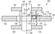
- FIG. 1 illustrates a cross-section of a magnetic sensor arrangement configured as angle sensor according to an exemplary embodiment.
- FIG. 2 illustrates another view of the magnetic sensor arrangement according to FIG. 1 .
- FIG. 3 illustrates a plan view of a magnetic sensor arrangement configured as angle sensor according to another exemplary embodiment.
- FIG. 4 illustrates a cross-sectional view of the magnetic sensor arrangement of FIG. 3 along a line B-B′.
- FIG. 5 illustrates a cross-sectional view of the magnetic sensor arrangement of FIG. 3 along a line A-A′.
- FIG. 6 illustrates a cross-sectional view of part of a magnetic sensor arrangement configured as angle sensor according to still another exemplary embodiment.
- FIG. 7 illustrates a three-dimensional view of a magnetic field generating structure of a magnetic sensor arrangement according to an exemplary embodiment.
- FIG. 8 illustrates a cross-sectional view of a magnetic sensor arrangement configured as angle sensor according to yet another exemplary embodiment.
- FIG. 9 illustrates a three-dimensional view of a magnetic field generating structure of a magnetic sensor arrangement configured as current sensor according to an exemplary embodiment.
- FIG. 10 to FIG. 13 illustrate cross sectional views of magnetic sensor arrangements with magnetic sensor packages according to exemplary embodiments.
- FIG. 14 and FIG. 15 illustrate cross sectional views of magnetic sensor arrangements with bare dies having a sensing element according to exemplary embodiments.
- the spacing of magnetic elements of a magnetic field generating structure should be close in order to increase the magnetic field in between them and to decrease the magnetic field far off the magnets (which may otherwise disturb nearby other equipment).
- Magnetic sensing elements may be housed in a magnetic sensor package, which may be mounted to a component board (for example a printed circuit board, PCB).
- the component board may have an accommodation hole to accommodate a shaft of the magnetic field generating structure. It is for instance also possible that the component board has the shape of a fork to define the accommodation hole.
- the component board may be placed between two magnetic elements, so the spacing of the magnetic elements should be large enough to accommodate the component board and the sensor package(s). If the component board is for example 1 mm thick and the magnetic sensor package is 1 mm thick, this means 2 mm plus some clearance of 1 mm above and below, which gives a minimum spacing between the magnets of around 4 mm.
- Exemplary embodiments of the invention may consider one or more of the above and other boundary conditions to provide a magnetic sensor arrangement with high detection accuracy.
- a first aspect of an exemplary embodiment of the invention allows to reduce the axial space consumption of the magnetic sensor arrangement or assembly.
- This may involve a specific design of an off-axis/through-shaft magnetic angle sensor, where the sensing elements are placed around a rotatable shaft.
- it is possible to provide a through-shaft to which two magnetic elements are mounted and a component board is placed between both magnetic elements (compare for example FIG. 1 ).
- the shaft and the magnetic elements may be rotatable as a whole, whereas the component board may be stationary.
- At least one magnetic sensor package may be mounted to the component board (for example, it is possible to mount three magnetic sensor packages at integer multiples of 120° on the same radius, which is concentric to the rotation axis).
- the component board may be configured with a shape of a fork so that it is possible to insert it between the magnetic elements without taking a magnetic element off the shaft.
- the component board it is also possible for the component board to have only an interior accommodation hole which accommodates the shaft.
- a task may be to arrange one or more magnetic sensor packages and the component board such that the clearances are of sufficient dimension, when the spacing of the two magnet elements has a certain predetermined value.
- a small spacing may be beneficial for large signals and small space consumption.
- the diameter of the magnetic elements scales with the spacing between them: smaller diameters correspond to a smaller axial gap between them, and vice versa. Then, in particular for small diameters, it may become challenging to insert a component board plus magnetic sensor package(s) and provide enough clearance to avoid collision.
- an advantage of an exemplary embodiment of the invention is that the axial position of the sensing element may be selected to be between both outer surfaces (i.e. bottom surface of component board and top surface of magnetic sensor package).
- the z-coordinate i.e. the vertical coordinate in a direction perpendicular to a symmetry plane of the component board, wherein this perpendicular direction can also be denoted as an axial direction in the context of this description
- the sensing element may be lower than the top surface of the component board. This may help to place the sensor element in the symmetry-plane of the magnetic elements (which corresponds to a center plane) so that the axial clearances above and below the component board may be increased, in particular may be maximized.
- the following exemplary embodiment shows how this principle may be implemented for a surface mounted device (SMD) package placed up-side down into an accommodation hole or recess in the component board (it is possible to provide a single magnetic sensor package, although several ones may be placed or distributed around the rotatable shaft).
- SMD surface mounted device
- the thickness of the component board is chosen so that the magnetic sensor package does not protrude at the bottom side of the component board or carrier this is highly advantageously, because then the component board protects the magnetic sensor package from collision with rotatable parts.
- a sensitive surface for instance the lower surface of the package portion in the accommodation hole in FIG.
- the sensitive surface may include bond wires and a silicon surface including a sensing element.
- the less sensitive surface may include a lead frame backside of the carrier.
- embodiments of the invention work also for leadless packages, for instance when the component board has no through-hole, but in contrast to this a recess forming a cavity (compare for instance FIG. 6 ).
- embodiments of the invention may work regardless of the orientation of a semiconductor chip (i.e. regardless of a face-up geometry, a face-down geometry, a flip-chip geometry, etc.).
- Exemplary embodiments of the invention may also be implemented for magnetic current sensors (so that applications of embodiments of the invention are not limited to angle sensors).
- the shaft carrying the magnetic element(s) may be replaced by a thick conductor and the magnetic field sensor(s) on the component board may detect the magnetic field generated by an electric current flowing through the conductor.
- the magnetic field sensor(s) on the component board may detect the magnetic field generated by an electric current flowing through the conductor.
- exemplary embodiments of the invention are particularly useful for off-axis/through-shaft magnetic angle sensors with two magnets having a narrow gap in-between.
- a magnetic sensor arrangement which comprises a component board comprising two main surfaces, preferably perpendicular to a vertical axis (i.e. top and bottom surfaces).
- the component board may comprise an accommodation hole (such as an aperture or a recess).
- At least one magnetic field sensing element may be located in and/or on a die, wherein the die may be housed in a magnetic sensor package comprising electric terminals.
- the magnetic sensor package may be mounted to the component board near the accommodation hole in such a way that the electric terminals of the magnetic sensor package are closer to the first of the two main surfaces than to the second of the two main surfaces, such that the spacing between the at least one magnetic field sensing element and the second of the two main surfaces is smaller than the axial spacing between the electric terminals and the second of the two main surfaces.
- the described arrangement may be configured as a magnetic current sensor, in which a conductor is passed through the accommodation hole in the component board.
- the die which may form the sensing element may protrude into the accommodation hole in a plan view along the vertical axis.
- the sensor package is a leadless package. At least one of the terminals may protrude laterally (i.e. in xy-plane) out of the magnetic sensor package.
- all terminals may protrude laterally out of the same surface of the magnetic sensor package (which may correspond to a leaded package architecture).
- the accommodation hole may be configured to accommodate a shaft which is rotatable around a z-axis or a conductor that passes through the accommodation hole.
- a magnetic field source or magnetic field generating structure may be attached to the shaft or may form an integral part thereof.
- the die is attached to a die-paddle of a leadframe and connected to electrical terminals made from the leadframe.
- a die-paddle may be a part of a lead frame.
- a singularized die or chip may be solderable or glueable on such a die-paddle.
- a second aspect of an exemplary embodiment of the invention (which may be combined with the first aspect) also allows to reduce the axial space consumption of the magnetic sensor assembly.
- an off-axis/through-shaft magnetic angle sensor may be provided in which the sensor elements may be placed around a rotatable shaft.
- an SMD package may be mounted on the component board, wherein the sensor die may be located at this side of the magnetic sensor package, which is opposite to the leads, which are soldered to the component board (such as a PCB). Since the thickness of the magnetic sensor package is roughly equal to the thickness of the component board, the axial position of the magnetic field sensing element(s) is shifted upwards, away from the symmetry center, such that an axial distance z in FIG. 8 may be much smaller than an axial distance y. If it is desired to place them in the symmetry center, it would be required to pull the magnetic elements further apart, and then the clearance between the component board and the lower magnetic element would be smaller than the clearance between the magnetic sensor package and the upper magnetic element, which is a waste in construction space. Moreover, if the shaft has an axial play, there is conventionally a certain risk that the magnetic element collides with the fragile top surface of the magnetic sensor package. This may cause the magnetic sensor arrangement to malfunction.
- An exemplary embodiment of the invention may place a sensor chip of the magnetic sensor package below the chip carrier (such as a leadframe) so that the sensing element(s) is/are oriented towards the same side as the solderable contact portions of the leads or terminals.
- the package may be mounted to the component board. So the sensing element(s) may be roughly mid-way in a sandwich structure comprising the component board and the magnetic sensor package, such that an axial distance x (for example a distance between sensing element and magnet) above and below the magnetic field sensing element(s) is identical or at least similar (for instance up to 33%).
- An advantage of protecting the fragile sensing element(s) from rotating parts also holds if there is only a single magnet portion without second magnet portion and without second ferrous shield. It is also possible to place the single rotating magnet portion below the component board in order to protect the magnetic sensor package from the rotating magnetic element.
- An advantage of exemplary embodiments of the invention may be more significant for small magnetic elements with for example outer diameters of roughly 25 mm, because then it may be desired to have small axial spacings between magnetic element(s) and sensing element(s) in the order of roughly 2 mm.
- the magnetic sensor package may have leads/pins on all four sides along its perimeter, or it may be a dual in-line type of magnetic sensor package which has leads/pins only on two opposite sides along its perimeter. Further alternatively, the magnetic sensor package may be a leaded type of package that has leads only on a single side along its perimeter. It may also be a leadless package that has solder pads on its mounting surface. These pads may populate the entire mounting surface or just a portion of the perimeter of the mounting surface. In particular it may have pads only on one, two or three sides of the perimeter. In all these cases, it may be beneficial if there are no lead/pins/pads near at least one side of the magnetic sensor package, namely this side which is closest to the rotating shaft.
- an angle sensor arrangement which comprises a shaft rotatable around a rotation axis, and a component board with an accommodation hole (such as an aperture or any other type of hole accommodating the shaft).
- a magnetic field source may be attached to the shaft.
- At least one magnetic field sensing element may be located in and/or on a substrate housed in at least one magnetic sensor package mounted to the component board.
- An axial spacing may be provided between the at least one magnetic field sensor element and the magnetic field source, wherein the magnetic field sensor element may be placed inside the magnetic sensor package so that it is closer to the mounting surface of the magnetic sensor package than to a second package surface, which is opposite the mounting surface of the package.
- the at least one magnetic sensor package may be located in a symmetry-plane of the magnetic field source, which may be perpendicular to the rotation axis.
- the substrate may be a silicon die.
- the magnetic sensor arrangement comprises at least one magnetic field sensing element and circuitry to read out its output signal (for instance in terms of signal conditioning).
- the at least one magnetic sensor package may comprise a leadframe, to which the sensor substrate may be mounted.
- the magnetic sensor package may be mounted on the component board so that the axial spacing between substrate and nearest rotatable part is larger than an axial spacing between leadframe and said nearest rotatable part.
- FIG. 1 illustrates a cross-section of a magnetic sensor arrangement 100 configured as angle sensor according to an exemplary embodiment.
- FIG. 2 illustrates another view of the magnetic sensor arrangement 100 according to FIG. 1 .
- the magnetic sensor arrangement 100 comprises a plate-shaped component board 104 , which is here embodied as a printed circuit board (PCB).
- the component board 104 is delimited by two opposing main surfaces 110 , 112 and has an accommodation hole 106 , here embodied as a through hole.
- the component board 104 can be a laminate of electrically conductive traces in a dielectric matrix.
- the accommodation hole 106 accommodates a rotatable (see rotation axis 199 and rotating arrow 197 ) shaft 130 of a magnetic field generating structure 102 .
- three magnetic sensor packages 108 are foreseen which are located partly between the two opposing main surfaces 110 , 112 and within the accommodation hole 106 .
- the magnetic sensor packages 108 are configured for sensing a respective local value of a magnetic field generated by the magnetic field generating structure 102 , more specifically generated by two axially spaced magnetic elements 132 thereof being fixedly mounted on the shaft 130 .
- the magnetic elements 132 are spaced vertically symmetrically with regard to an axial symmetry plane 195 .
- the magnetic sensor packages 108 are mounted at main surface 110 and extend into the accommodation hole 106 .
- Each of the magnetic sensor packages 108 comprises a sensing element 114 (being provided on or forming part of a semiconductor chip 189 ) mounted on an electrically conductive carrier 116 .
- Both the sensing element 114 (fully) and the carrier 116 (partially) are encapsulated by an encapsulant 118 which may be a dielectric mold compound.
- the sensing elements 114 and part of the encapsulants 118 are located in the accommodation hole 106 .
- the carriers 116 are mounted at the main surface 110 .
- the carriers 116 i.e. the lead frames
- the carriers 116 are embodied as flat conductors and are entirely located outside of the accommodation hole 106 (wherein the accommodation hole 106 is laterally delimited by the vertical wall of the component board 104 and is vertically delimited by the vanishing lines of the upper main surface 110 and the lower main surface 112 ).
- the magnetic sensor packages 108 are leaded sensor packages. Terminals 124 extend out of the respective magnetic sensor package 108 and extend along and parallel to main surface 110 . More specifically, all terminals 124 extend out of the respectively same side edge 150 of the respective magnetic sensor package 108 .
- the magnetic field generating structure 102 comprises the rotatable shaft 130 , being rotatable relative to the component board 104 and the magnetic sensor packages 108 . Furthermore, the magnetic field generating structure 102 comprises the two symmetrically positioned magnetic elements 132 which may be of a permanent magnetic material with asymmetric magnetic properties with regard to a rotation angle to be sensed. The magnetic elements 132 are disk-shaped with a thickness varying within a plane perpendicular to the shaft axis.
- three magnetic sensor packages 108 are located partially between the two opposing main surfaces 110 , 112 and are each configured for sensing a magnetic field generated by the magnetic field generating structure 102 .
- the magnetic sensor packages 108 are hence configured for sensing a magnetic field at different circumferential positions around the magnetic field generating structure 102 . This provides a spatial magnetic field profile and hence increases accuracy of the detection.
- the elevation view of FIG. 1 shows an equal spacing d in a vertical direction between the magnetic elements 132 and a vertical position of the sensing element 114 of the respective magnetic sensor package 108 .
- An axial distance s between an upper end of the respective magnetic sensor package 108 and a lower surface of the upper magnetic element 132 can be kept very small due to the spatial arrangement of the individual components of the magnetic sensor arrangement 100 according to FIG. 1 .
- a small radial clearance 1 i.e. a radial distance between a cylindrical surface of the rotatable shaft 130 and the radially inner end of the respective magnetic sensor package 108 can be kept very small.
- an axial clearance b between an upper surface of the lower magnetic element 132 and lower main surface 112 of the component board 104 can be kept quite small, and for instance identical or very similar to the axial clearance s.
- a bulky portion of a respective magnetic sensor package 108 which extends downwardly from the exposed portion of the flat or sheet-like carrier 116 extends into the accommodation hole 106 and therefore does not contribute significantly to the vertical thickness of the sensing portion of the magnetic sensor arrangement 100 according to FIG. 1 .
- the leaded packages constituting the magnetic sensor packages 108 according to FIG. 1 protrude into the aperture or accommodation hole 106 of the PCB-type component board 104 and are oriented face-down.
- FIG. 2 shows how the three leaded magnetic sensor packages 108 are distributed around a circumference of the cylindrical shaft 130 , wherein each two neighboured magnetic sensor packages 108 are spaced with regard to one another by 120°. This allows to properly detect the magnetic profile around the shaft 130 .
- the shaft 130 rotates with a certain angular velocity. Due to the angularly asymmetric configuration of the magnetic elements 132 (compare FIG. 7 ), the sensing elements 114 detect a respective magnetic field value which is a clear fingerprint for the present angular position of the magnetic elements 132 and therefore of the shaft 130 on which the magnetic elements 132 are rigidly mounted so as to rotate together with the shaft 130 . Since the position of the respective sensing element 114 is quite close to the radial center of the shaft 132 and is located symmetrically with regard to the two magnetic elements 132 , a high accuracy of the detection result can be obtained.
- FIG. 3 illustrates a plan view of a magnetic sensor arrangement 100 configured as angle sensor according to another exemplary embodiment.
- FIG. 4 illustrates a cross-sectional view of the magnetic sensor arrangement 100 of FIG. 3 along a line B-B′.
- FIG. 5 illustrates a cross-sectional view of the magnetic sensor arrangement 100 of FIG. 3 along a line A-A′.
- the magnetic sensor package 108 is a Surface Mounted Device (SMD) sensor package.
- SMD Surface Mounted Device
- a plurality of terminals 124 extend out of two opposing side edges 150 , 152 of the magnetic sensor package 108 .
- the carrier 116 is here a curved leadframe and is located partially inside and partially outside of the accommodation hole 106 .
- the accommodation hole 106 is here configured so that the component board 104 has a fork-shaped design. This simplifies insertion of the shaft 102 into the accommodation hole 106 to a desired position.
- the magnetic sensor package 108 extends vertically into a narrow hole section at an innermost position of the accommodation hole 106 . With this geometry, assembly or disassembly of the shaft 102 is not disturbed by the magnetic sensor package 108 .
- end portions of the carrier 116 may be soldered to main surface 110 of the component board 104 .
- the sensing element 114 on the semiconductor chip 189 is mounted on a die-paddle 182 of the carrier 116 .
- Elements 182 , 114 , 189 are encapsulated by encapsulant 118 .
- a bent portion of the carrier 116 as well as the sensing element 114 and a major portion of the encapsulant 118 are located in the accommodation hole 106 and therefore do not add significantly to the thickness of the sensor portion of the magnetic sensor arrangement 100 according to FIG. 3 to FIG. 5 .
- terminals 124 of a bent lead frame are exposed on two opposing side edges 150 , 152 of the magnetic sensor package 108 .
- FIG. 6 illustrates a cross-sectional view of a magnetic sensor arrangement 100 configured as angle sensor according to still another exemplary embodiment.
- the magnetic sensor package 108 is mounted in a cavity 120 and on a third surface 122 located between and parallel to the opposing main surfaces 110 , 112 of the component board 104 .
- the architecture according to FIG. 6 corresponds to a leadless sensor package configuration of the magnetic sensor package 108 .
- the carrier 116 of the lead frame type shown in FIG. 6 can be manufactured by half etching.
- a bottom of the magnetic sensor package 108 does not or not significantly extend beyond a bottom of the component board 104 .
- the thickness of the component board 104 is such that the axial position of the sensing element 114 is in the middle between top surface 110 and bottom surface 112 of the component board 104 .
- FIG. 7 illustrates a three-dimensional view of a magnetic field generating structure 102 of a magnetic sensor arrangement 100 according to an exemplary embodiment.
- the three-dimensional view of the magnetic field generating structure 102 shown in FIG. 7 illustrates that the latter is composed of a for instance ferrous rotatable cylindrical shaft 130 on which, axially spaced apart, two magnetic elements 132 are rigidly mounted so as to rotate together with the shaft 130 .
- the thickness of both magnetic elements 132 varies along a circumference of the shaft 130 , wherein a thickness at a certain angular position of one of the magnetic elements 132 corresponds to a thickness of the other of the magnetic elements 132 at this angular position.
- the two magnetic elements 132 are disk-shaped with circumferentially varying thickness. This allows a sensing element 114 (not shown in FIG.
- the maximum magnetic field can be for instance +50 mT.
- the maximum magnetic field can be for instance ⁇ 50 mT.
- the magnetic field can be for instance 0 mT.
- the portions of the magnetic elements 132 shown on the right-hand side of FIG. 7 are magnetized in positive z-direction, whereas the portions of the magnetic elements 132 shown on the left-hand side of FIG. 7 are magnetized in negative z-direction.
- the rotational axis corresponds to the vertical axis according to FIG. 7 .
- the circumferentially varying thickness of the magnetic element 132 provides for a circumferential modulation of the intensity of the axial magnetic field.
- an alternative configuration of the magnetic elements 132 is the provision of disk-shaped magnetic elements 132 with circumferentially homogeneous thickness but circumferentially inhomogeneous magnetization.
- FIG. 8 illustrates a cross-sectional view of a magnetic sensor arrangement 100 configured as angle sensor according to yet another exemplary embodiment.
- FIG. 8 compares a conventional magnetic sensor arrangement 200 on the left-hand side with a magnetic sensor arrangement 100 according to an exemplary embodiment of the invention on the right-hand side.
- FIG. 8 On the left-hand side of FIG. 8 , it can be seen that a sensing element 202 and an encapsulant 204 are arranged on a convex portion of a curved carrier 208 , so that the sensing element 202 faces away from component board 210 . This results in a large vertical thickness of the sensor portion of the magnetic sensor arrangement 220 . Therefore, magnetic elements 222 need to be far away from the component board 204 which reduces the accuracy of the detection.
- FIG. 8 This embodiment relates to the shown magnetic sensor arrangement 100 which comprises component board 104 , embodied as PCB.
- the component board 104 has an accommodation hole 106 for accommodating part of a magnetic field generating structure 102 , i.e. part of shaft 130 .
- the magnetic field generating structure 102 mounts the magnetic elements 132 on the shaft 130 via a holder 183 and fastening elements 181 such as screws.
- a magnetic sensor package 108 is mounted on the component board 104 and is configured for sensing a magnetic field generated by the magnetic field generating structure 102 .
- the magnetic sensor package 108 comprises sensing element 114 on carrier 116 .
- the sensing element 114 extends from the carrier 116 towards the component board 104 . Moreover, the sensing element 114 is arranged between the carrier 116 and the component board 104 . According to the embodiment of FIG. 8 , the carrier 116 is curved to thereby form a cavity 185 in which the sensing element 114 is at least partially accommodated.
- the magnetic sensor arrangement 100 of FIG. 8 comprises an encapsulant 118 , in which the sensing element 114 and the part of the carrier 116 are encapsulated, for instance a mold compound.
- the encapsulant 118 is arranged partly between the carrier 116 and the component board 104 , and extends partly beyond the carrier 116 in an upward direction.
- the carrier 116 is mounted on main surface 110 of the component board 104 .
- the sensing element 114 may be for example located inside the magnetic sensor package 108 so as to be located closer to a mounting surface 110 of the magnetic sensor package 108 than to another magnetic sensor package surface opposing the mounting surface 110 .
- the magnetic sensor package 108 may be located also in or close to a symmetry plane of the magnetic field generating structure 102 . It may be for instance mounted on the component board 104 so that an axial spacing between the sensing element 114 and a nearest rotatable portion of the magnetic field generating structure 102 is larger than an axial spacing between the carrier 116 and the nearest rotatable portion.
- the sensing element 114 on its semiconductor chip 189 is mounted on a concave portion of the two-dimensionally curved carrier 116 and is therefore arranged in cavity 185 so that it does not add to the vertical thickness of the sensor portion of the magnetic sensor arrangement 100 according to FIG. 8 .
- This allows the magnetic elements 132 to be spaced axially with a smaller distance, which in turn increases the detection accuracy.
- the semiconductor chip (see reference numeral 189 on the right-hand side) is mounted above the carrier 208 on the left-hand side and is mounted below the carrier 116 on the right-hand side.
- the thickness of the magnetic sensor package (see reference numeral 108 on the right-hand side) differs by the thickness of the semiconductor chip 189 , i.e. around 0.2 mm.
- the sensing element 202 in the arrangement on the left-hand side is significantly further away from the symmetry plane of the magnetic field than on the right-hand side, where the sensing element 114 is very close to or exactly in the symmetry plane.
- the conventional configuration on the left-hand side of FIG. 8 may be obtained by bending legs of a lead frame away from the sensing element 202
- the configuration on the right-hand side of FIG. 8 according to an exemplary embodiment may be obtained by bending legs of a lead frame towards the sensing element 114 .
- FIG. 9 illustrates a three-dimensional view of a magnetic field generating structure 102 of a magnetic sensor arrangement 100 configured as current sensor according to an exemplary embodiment.
- the magnetic field generating structure 102 comprises an electrically conductive structure 140 through which an electric current, which is to be sensed, can flow.
- FIG. 9 shows hence a configuration in which an electric current I flows through an electrically conductive conductor as magnetic field generating structure 102 . Consequently, a magnetic field B is generated in the event of a current flow. The value of this magnetic field can be sensed by the sensing element 114 of the magnetic sensor package 108 .
- FIG. 10 illustrates a cross sectional view of a magnetic sensor arrangement 100 with a magnetic sensor package 108 according to an exemplary embodiment.
- the magnetic sensor arrangement 100 shown in FIG. 10 comprises a component board 104 having a first vertical thickness T 1 .
- a magnetic sensor package 108 is provided with a second vertical thickness T 2 and is mounted on the component board 104 .
- a sensing element 114 of the magnetic sensor package 108 is configured for sensing a magnetic field generated by a magnetic field generating structure (not shown in FIG. 10 ).
- the sensing element 114 is located vertically not more than one third of the sum of the first vertical thickness T 1 and the second vertical thickness T 2 away from a vertical center M vertically in the middle between an upper end and a lower end of the shown assembly composed of the component board 104 and the magnetic sensor package 108 mounted thereon.
- T denotes the entire vertical thickness of the arrangement shown in FIG. 10 .
- the vertical displacement h of the sensing element 114 from the middle or vertical center M is less than one third (preferably is less than a quarter) of the sum of the individual vertical thicknesses T 1 plus T 2 .
- Z 1 and Z 2 denote the vertical spacing of the sensing element 114 from a top end and a bottom end, respectively, of the arrangement shown in FIG. 10 .
- FIG. 11 illustrates a cross sectional view of a magnetic sensor arrangement 100 with a magnetic sensor package 108 according to another exemplary embodiment.
- Figure shows a similar situation as FIG. 10 for a leaded package.
- FIG. 12 illustrates a cross sectional view of a magnetic sensor arrangement 100 with a magnetic sensor package 108 according to another exemplary embodiment.
- FIG. 12 shows a similar situation as FIG. 10 for an SMD package.
- FIG. 13 illustrates a cross sectional view of a magnetic sensor arrangement 100 with a magnetic sensor package 108 according to another exemplary embodiment.
- Figure shows a similar situation as FIG. 10 for a leadless package.
- FIG. 14 illustrates a cross sectional view of a magnetic sensor arrangement 100 with a bare die in form of semiconductor chip 189 having a sensing element 114 according to an exemplary embodiment.
- a bare semiconductor chip 189 rather than a package is provided.
- Balls or bumps for providing a connection with the component board 104 are denoted with reference numeral 111 .
- An underfill is denoted with reference numeral 113 .
- FIG. 14 relates to a flip chip configuration.
- FIG. 15 illustrates a cross sectional view of a magnetic sensor arrangement 100 with a bare die in form of semiconductor chip 189 having a sensing element 114 according to another exemplary embodiment.
Landscapes
- Physics & Mathematics (AREA)
- General Physics & Mathematics (AREA)
- Condensed Matter Physics & Semiconductors (AREA)
- Engineering & Computer Science (AREA)
- Manufacturing & Machinery (AREA)
- Measuring Magnetic Variables (AREA)
- Hall/Mr Elements (AREA)
- Measurement Of Length, Angles, Or The Like Using Electric Or Magnetic Means (AREA)
Abstract
Description
Claims (1)
Priority Applications (1)
| Application Number | Priority Date | Filing Date | Title |
|---|---|---|---|
| US17/107,530 US11506728B2 (en) | 2016-04-27 | 2020-11-30 | Compact sensor package |
Applications Claiming Priority (2)
| Application Number | Priority Date | Filing Date | Title |
|---|---|---|---|
| DE102016107798.4A DE102016107798B4 (en) | 2016-04-27 | 2016-04-27 | Compact sensor package |
| DE102016107798.4 | 2016-04-27 |
Related Child Applications (1)
| Application Number | Title | Priority Date | Filing Date |
|---|---|---|---|
| US17/107,530 Division US11506728B2 (en) | 2016-04-27 | 2020-11-30 | Compact sensor package |
Publications (2)
| Publication Number | Publication Date |
|---|---|
| US20170314969A1 US20170314969A1 (en) | 2017-11-02 |
| US11079446B2 true US11079446B2 (en) | 2021-08-03 |
Family
ID=60081855
Family Applications (2)
| Application Number | Title | Priority Date | Filing Date |
|---|---|---|---|
| US15/497,296 Active 2038-04-10 US11079446B2 (en) | 2016-04-27 | 2017-04-26 | Compact sensor package |
| US17/107,530 Active 2037-04-28 US11506728B2 (en) | 2016-04-27 | 2020-11-30 | Compact sensor package |
Family Applications After (1)
| Application Number | Title | Priority Date | Filing Date |
|---|---|---|---|
| US17/107,530 Active 2037-04-28 US11506728B2 (en) | 2016-04-27 | 2020-11-30 | Compact sensor package |
Country Status (3)
| Country | Link |
|---|---|
| US (2) | US11079446B2 (en) |
| CN (1) | CN107450035B (en) |
| DE (1) | DE102016107798B4 (en) |
Cited By (1)
| Publication number | Priority date | Publication date | Assignee | Title |
|---|---|---|---|---|
| US20250224458A1 (en) * | 2024-01-04 | 2025-07-10 | Allegro Microsystems, Llc | System and method to monitor power source connections |
Families Citing this family (17)
| Publication number | Priority date | Publication date | Assignee | Title |
|---|---|---|---|---|
| US10591274B2 (en) | 2016-09-28 | 2020-03-17 | Infineon Technologies Ag | External field robust angle sensing with differential magnetic field |
| US10509058B2 (en) | 2018-01-12 | 2019-12-17 | Allegro Microsystems, Llc | Current sensor using modulation of or change of sensitivity of magnetoresistance elements |
| US10578684B2 (en) | 2018-01-12 | 2020-03-03 | Allegro Microsystems, Llc | Magnetic field sensor having magnetoresistance elements with opposite bias directions |
| DE102018111216B3 (en) * | 2018-05-09 | 2019-10-17 | Semikron Elektronik Gmbh & Co. Kg | Circuit arrangement for current measurement in a power semiconductor group and power semiconductor module hereby |
| US10734443B2 (en) | 2018-08-27 | 2020-08-04 | Allegro Microsystems, Llc | Dual manetoresistance element with two directions of response to external magnetic fields |
| US10670669B2 (en) | 2018-10-11 | 2020-06-02 | Allegro Microsystems, Llc | Magnetic field sensor for measuring an amplitude and a direction of a magnetic field using one or more magnetoresistance elements having reference layers with the same magnetic direction |
| US10746820B2 (en) | 2018-10-11 | 2020-08-18 | Allegro Microsystems, Llc | Magnetic field sensor that corrects for the effect of a stray magnetic field using one or more magnetoresistance elements, each having a reference layer with the same magnetic direction |
| US10699976B1 (en) * | 2019-01-29 | 2020-06-30 | Infineon Technologies Ag | Semiconductor module with external power sensor |
| DE102020105933A1 (en) * | 2019-03-06 | 2020-09-10 | Infineon Technologies Ag | COMPARED TO AN EXTERNAL FIELD, ROBUST ANGLE DETECTION WITH DIFFERENTIAL MAGNETIC FIELD |
| US10866287B1 (en) | 2019-07-10 | 2020-12-15 | Allegro Microsystems, Llc | Magnetic field sensor with magnetoresistance elements arranged in a bridge and having a common reference direction and opposite bias directions |
| US11118945B2 (en) * | 2019-09-27 | 2021-09-14 | Praxair Technology, Inc. | Apparatus for mounting and aligning an angular position sensor to a rotating shaft |
| DE102020210407A1 (en) | 2020-08-17 | 2022-02-17 | Robert Bosch Gesellschaft mit beschränkter Haftung | Rotary machine with position sensor |
| US11719771B1 (en) | 2022-06-02 | 2023-08-08 | Allegro Microsystems, Llc | Magnetoresistive sensor having seed layer hysteresis suppression |
| US12130342B2 (en) | 2022-06-10 | 2024-10-29 | Allegro Microsystems, Llc | Magnetic field current sensor to reduce stray magnetic fields |
| US12320870B2 (en) | 2022-07-19 | 2025-06-03 | Allegro Microsystems, Llc | Controlling out-of-plane anisotropy in an MR sensor with free layer dusting |
| US12181538B2 (en) | 2022-11-29 | 2024-12-31 | Allegro Microsystems, Llc | Magnetoresistance bridge circuits with stray field immunity |
| US12347595B2 (en) | 2023-06-13 | 2025-07-01 | Allegro Microsystems, Llc | Magnetoresistance element including a skyrmion layer and a vortex layer that are magnetically coupled to each other |
Citations (17)
| Publication number | Priority date | Publication date | Assignee | Title |
|---|---|---|---|---|
| JPH01129678U (en) | 1988-02-18 | 1989-09-04 | ||
| US5831596A (en) * | 1992-03-25 | 1998-11-03 | Penney & Giles Blackwood Limited | Joystick controller using magnetic position sensors and a resilient control arm with sensor used to measure its flex |
| US20040085062A1 (en) | 2002-10-30 | 2004-05-06 | Hitachi, Ltd. And Hitachi Car Engineering Co., Ltd | Noncontact rotary position sensor and electric control throttle valve apparatus having noncontact rotary position |
| US20040160220A1 (en) * | 2001-07-03 | 2004-08-19 | Matthias Wendt | Arrangement for measuring the angular position of an object |
| JP2006258592A (en) | 2005-03-17 | 2006-09-28 | Nikkoshi Co Ltd | Hall probe |
| US20070229067A1 (en) * | 2006-03-30 | 2007-10-04 | Alps Electric Co., Ltd. | Magnetic sensor having resistance adjusting unit and method of manufacturing the same |
| US20070252591A1 (en) | 2002-05-15 | 2007-11-01 | Siemens Vdo Automotive Corporatin | Through the hole rotary position sensor |
| DE102008012665A1 (en) | 2008-03-05 | 2009-09-10 | Conti Temic Microelectronic Gmbh | Current measuring device by means of magnet-sensitive sensor for a power electronic system |
| DE102011001194A1 (en) | 2010-03-12 | 2011-11-10 | Denso Corporation | Sensor unit and magnetic flux concentrating module |
| US20120105057A1 (en) * | 2009-07-15 | 2012-05-03 | Skf B.V. | Hall-effect sensor arrangement |
| US20130021025A1 (en) * | 2011-07-18 | 2013-01-24 | Honeywell International Inc. | Stationary magnet variable reluctance magnetic sensors |
| US20130305843A1 (en) * | 2012-05-17 | 2013-11-21 | Lg Innotek Co., Ltd. | Torque Angle Sensor |
| US20140070801A1 (en) * | 2012-05-16 | 2014-03-13 | Alps Green Devices Co., Ltd. | Current sensor |
| US20140253109A1 (en) * | 2013-03-08 | 2014-09-11 | Deere & Company | Method and sensor for sensing current in a conductor |
| CN104296650A (en) | 2013-07-17 | 2015-01-21 | 英飞凌科技股份有限公司 | Discrete magnetic angle sensor device, a magnetic angle sensor arrangement, a method for generating an angle signal and a method for providing a sensor signal |
| US20150123650A1 (en) | 2012-09-28 | 2015-05-07 | Alps Green Devices Co., Ltd. | Current sensor |
| US20150369679A1 (en) | 2014-06-18 | 2015-12-24 | Jtekt Corporation | Torque sensor and electric power steering system |
Family Cites Families (1)
| Publication number | Priority date | Publication date | Assignee | Title |
|---|---|---|---|---|
| JP6268799B2 (en) * | 2013-08-07 | 2018-01-31 | アイシン精機株式会社 | Current sensor |
-
2016
- 2016-04-27 DE DE102016107798.4A patent/DE102016107798B4/en active Active
-
2017
- 2017-04-26 US US15/497,296 patent/US11079446B2/en active Active
- 2017-04-27 CN CN201710288298.4A patent/CN107450035B/en active Active
-
2020
- 2020-11-30 US US17/107,530 patent/US11506728B2/en active Active
Patent Citations (20)
| Publication number | Priority date | Publication date | Assignee | Title |
|---|---|---|---|---|
| JPH01129678U (en) | 1988-02-18 | 1989-09-04 | ||
| US5831596A (en) * | 1992-03-25 | 1998-11-03 | Penney & Giles Blackwood Limited | Joystick controller using magnetic position sensors and a resilient control arm with sensor used to measure its flex |
| US20040160220A1 (en) * | 2001-07-03 | 2004-08-19 | Matthias Wendt | Arrangement for measuring the angular position of an object |
| US20070252591A1 (en) | 2002-05-15 | 2007-11-01 | Siemens Vdo Automotive Corporatin | Through the hole rotary position sensor |
| US20040085062A1 (en) | 2002-10-30 | 2004-05-06 | Hitachi, Ltd. And Hitachi Car Engineering Co., Ltd | Noncontact rotary position sensor and electric control throttle valve apparatus having noncontact rotary position |
| JP2006258592A (en) | 2005-03-17 | 2006-09-28 | Nikkoshi Co Ltd | Hall probe |
| US20070229067A1 (en) * | 2006-03-30 | 2007-10-04 | Alps Electric Co., Ltd. | Magnetic sensor having resistance adjusting unit and method of manufacturing the same |
| DE102008012665A1 (en) | 2008-03-05 | 2009-09-10 | Conti Temic Microelectronic Gmbh | Current measuring device by means of magnet-sensitive sensor for a power electronic system |
| US20120105057A1 (en) * | 2009-07-15 | 2012-05-03 | Skf B.V. | Hall-effect sensor arrangement |
| DE102011001194A1 (en) | 2010-03-12 | 2011-11-10 | Denso Corporation | Sensor unit and magnetic flux concentrating module |
| US20130021025A1 (en) * | 2011-07-18 | 2013-01-24 | Honeywell International Inc. | Stationary magnet variable reluctance magnetic sensors |
| US20140070801A1 (en) * | 2012-05-16 | 2014-03-13 | Alps Green Devices Co., Ltd. | Current sensor |
| US20130305843A1 (en) * | 2012-05-17 | 2013-11-21 | Lg Innotek Co., Ltd. | Torque Angle Sensor |
| US20150300898A1 (en) | 2012-05-17 | 2015-10-22 | Lg Innotek Co., Ltd. | Torque Angle Sensor |
| US20150123650A1 (en) | 2012-09-28 | 2015-05-07 | Alps Green Devices Co., Ltd. | Current sensor |
| US20140253109A1 (en) * | 2013-03-08 | 2014-09-11 | Deere & Company | Method and sensor for sensing current in a conductor |
| CN104296650A (en) | 2013-07-17 | 2015-01-21 | 英飞凌科技股份有限公司 | Discrete magnetic angle sensor device, a magnetic angle sensor arrangement, a method for generating an angle signal and a method for providing a sensor signal |
| US20150022192A1 (en) * | 2013-07-17 | 2015-01-22 | Infineon Technologies Ag | Discrete magnetic angle sensor device, a magnetic angle sensor arrangement, a method for generating an angle signal and a method for providing a sensor signal |
| DE102014110019A1 (en) | 2013-07-17 | 2015-06-11 | Infineon Technologies Ag | DISCRETE MAGNETIC ANGLE SENSOR DEVICE, MAGNETIC ANGLE SENSOR ARRANGEMENT, METHOD FOR GENERATING AN ANGLE SIGNAL, AND METHOD FOR PREPARING A SENSOR SIGNAL |
| US20150369679A1 (en) | 2014-06-18 | 2015-12-24 | Jtekt Corporation | Torque sensor and electric power steering system |
Cited By (2)
| Publication number | Priority date | Publication date | Assignee | Title |
|---|---|---|---|---|
| US20250224458A1 (en) * | 2024-01-04 | 2025-07-10 | Allegro Microsystems, Llc | System and method to monitor power source connections |
| US12474414B2 (en) * | 2024-01-04 | 2025-11-18 | Allegro Microsystems, Llc | System and method to monitor power source connections |
Also Published As
| Publication number | Publication date |
|---|---|
| US20170314969A1 (en) | 2017-11-02 |
| CN107450035A (en) | 2017-12-08 |
| DE102016107798B4 (en) | 2020-12-10 |
| US11506728B2 (en) | 2022-11-22 |
| CN107450035B (en) | 2022-04-08 |
| DE102016107798A1 (en) | 2017-11-02 |
| US20210080516A1 (en) | 2021-03-18 |
Similar Documents
| Publication | Publication Date | Title |
|---|---|---|
| US11506728B2 (en) | Compact sensor package | |
| US10254103B2 (en) | Arrangements for magnetic field sensors that act as tooth detectors | |
| JP6463789B2 (en) | Magnetic angular position sensor | |
| US9411025B2 (en) | Integrated circuit package having a split lead frame and a magnet | |
| US9547024B2 (en) | Device for current measurement | |
| US10048295B2 (en) | Current sensor | |
| US20130200883A1 (en) | Magnetic field sensor | |
| US10288449B2 (en) | Detection of a rotational position of a shaft | |
| US10663533B2 (en) | Calibration of a current sensor | |
| US12402541B2 (en) | Stacked die assembly | |
| US11448525B2 (en) | Sensor devices with test magnets, and associated methods | |
| US10605625B2 (en) | Measuring system | |
| JP5356793B2 (en) | Magnetic detection device and manufacturing method thereof | |
| US11879729B2 (en) | Measurement arrangement and sensor package | |
| US12326482B2 (en) | Magnetic system for counting rotations having increased stability against magnetic interference fields |
Legal Events
| Date | Code | Title | Description |
|---|---|---|---|
| AS | Assignment |
Owner name: INFINEON TECHNOLOGIES AG, GERMANY Free format text: ASSIGNMENT OF ASSIGNORS INTEREST;ASSIGNORS:AUSSERLECHNER, UDO;HOLLIBER, MICHAEL;REEL/FRAME:042146/0068 Effective date: 20170424 |
|
| STPP | Information on status: patent application and granting procedure in general |
Free format text: DOCKETED NEW CASE - READY FOR EXAMINATION |
|
| STPP | Information on status: patent application and granting procedure in general |
Free format text: NON FINAL ACTION MAILED |
|
| STPP | Information on status: patent application and granting procedure in general |
Free format text: RESPONSE TO NON-FINAL OFFICE ACTION ENTERED AND FORWARDED TO EXAMINER |
|
| STPP | Information on status: patent application and granting procedure in general |
Free format text: FINAL REJECTION MAILED |
|
| STPP | Information on status: patent application and granting procedure in general |
Free format text: DOCKETED NEW CASE - READY FOR EXAMINATION |
|
| STPP | Information on status: patent application and granting procedure in general |
Free format text: NON FINAL ACTION MAILED |
|
| STPP | Information on status: patent application and granting procedure in general |
Free format text: RESPONSE TO NON-FINAL OFFICE ACTION ENTERED AND FORWARDED TO EXAMINER |
|
| STPP | Information on status: patent application and granting procedure in general |
Free format text: NOTICE OF ALLOWANCE MAILED -- APPLICATION RECEIVED IN OFFICE OF PUBLICATIONS |
|
| STPP | Information on status: patent application and granting procedure in general |
Free format text: NOTICE OF ALLOWANCE MAILED -- APPLICATION RECEIVED IN OFFICE OF PUBLICATIONS |
|
| STPP | Information on status: patent application and granting procedure in general |
Free format text: PUBLICATIONS -- ISSUE FEE PAYMENT RECEIVED |
|
| STPP | Information on status: patent application and granting procedure in general |
Free format text: PUBLICATIONS -- ISSUE FEE PAYMENT VERIFIED |
|
| STCF | Information on status: patent grant |
Free format text: PATENTED CASE |
|
| MAFP | Maintenance fee payment |
Free format text: PAYMENT OF MAINTENANCE FEE, 4TH YEAR, LARGE ENTITY (ORIGINAL EVENT CODE: M1551); ENTITY STATUS OF PATENT OWNER: LARGE ENTITY Year of fee payment: 4 |