US11070402B2 - Receiving apparatus and receiving method - Google Patents
Receiving apparatus and receiving method Download PDFInfo
- Publication number
- US11070402B2 US11070402B2 US16/555,434 US201916555434A US11070402B2 US 11070402 B2 US11070402 B2 US 11070402B2 US 201916555434 A US201916555434 A US 201916555434A US 11070402 B2 US11070402 B2 US 11070402B2
- Authority
- US
- United States
- Prior art keywords
- binary data
- waveform
- received signal
- appearance frequency
- data
- Prior art date
- Legal status (The legal status is an assumption and is not a legal conclusion. Google has not performed a legal analysis and makes no representation as to the accuracy of the status listed.)
- Active
Links
Images


Classifications
-
- H—ELECTRICITY
- H04—ELECTRIC COMMUNICATION TECHNIQUE
- H04L—TRANSMISSION OF DIGITAL INFORMATION, e.g. TELEGRAPHIC COMMUNICATION
- H04L7/00—Arrangements for synchronising receiver with transmitter
- H04L7/02—Speed or phase control by the received code signals, the signals containing no special synchronisation information
- H04L7/033—Speed or phase control by the received code signals, the signals containing no special synchronisation information using the transitions of the received signal to control the phase of the synchronising-signal-generating means, e.g. using a phase-locked loop
- H04L7/0334—Processing of samples having at least three levels, e.g. soft decisions
-
- H—ELECTRICITY
- H04—ELECTRIC COMMUNICATION TECHNIQUE
- H04L—TRANSMISSION OF DIGITAL INFORMATION, e.g. TELEGRAPHIC COMMUNICATION
- H04L25/00—Baseband systems
- H04L25/02—Details ; arrangements for supplying electrical power along data transmission lines
- H04L25/03—Shaping networks in transmitter or receiver, e.g. adaptive shaping networks
- H04L25/03006—Arrangements for removing intersymbol interference
- H04L25/03012—Arrangements for removing intersymbol interference operating in the time domain
- H04L25/03019—Arrangements for removing intersymbol interference operating in the time domain adaptive, i.e. capable of adjustment during data reception
- H04L25/03057—Arrangements for removing intersymbol interference operating in the time domain adaptive, i.e. capable of adjustment during data reception with a recursive structure
-
- H—ELECTRICITY
- H04—ELECTRIC COMMUNICATION TECHNIQUE
- H04L—TRANSMISSION OF DIGITAL INFORMATION, e.g. TELEGRAPHIC COMMUNICATION
- H04L25/00—Baseband systems
- H04L25/02—Details ; arrangements for supplying electrical power along data transmission lines
- H04L25/03—Shaping networks in transmitter or receiver, e.g. adaptive shaping networks
- H04L25/03828—Arrangements for spectral shaping; Arrangements for providing signals with specified spectral properties
- H04L25/03834—Arrangements for spectral shaping; Arrangements for providing signals with specified spectral properties using pulse shaping
- H04L25/03853—Shaping by digital methods other than look up tables or up/down converters
-
- H—ELECTRICITY
- H04—ELECTRIC COMMUNICATION TECHNIQUE
- H04L—TRANSMISSION OF DIGITAL INFORMATION, e.g. TELEGRAPHIC COMMUNICATION
- H04L25/00—Baseband systems
- H04L25/02—Details ; arrangements for supplying electrical power along data transmission lines
- H04L25/03—Shaping networks in transmitter or receiver, e.g. adaptive shaping networks
- H04L25/03878—Line equalisers; line build-out devices
- H04L25/03885—Line equalisers; line build-out devices adaptive
Definitions
- Embodiments described herein relate generally to a receiving apparatus and a receiving method.
- Serial interface standards such as PCI Express (registered trademark) standard (hereinafter referred to as PCIe (registered trademark)) provide a specification called lane margining (hereinafter referred to as “LM”) for monitoring an eye pattern of a received signal.
- PCIe registered trademark
- LM lane margining
- the sample circuit for LM has a configuration capable of adjusting a reference voltage which is a threshold voltage with respect to the eye pattern and offset values of time. The eye pattern is acquired by comparing a determination result of the sample circuit for LM with a determination result without offset by the data sample circuit.
- ISI inter-symbol interference
- a method may be considered where another sample circuit having a different reference voltage in addition to the sample circuit for LM, is provided in parallel at a stage subsequent to an equalizer at an input end of the received circuit.
- the method is not preferable because of increasing a load on an input end of the data sample circuit due to an increase of a parasitic capacitance or the like, which may cause deterioration of waveform quality.
- FIG. 1 is a block diagram showing a portion of a circuit configuration of a receiving apparatus according to one embodiment.
- FIGS. 2A, 2B, and 2C are diagrams conceptually showing processing performed by a waveform processing unit according to one embodiment.
- FIG. 3 is a flowchart showing specific processing of waveform data generation performed by the waveform processing unit according to one embodiment.
- FIGS. 4A, 4B, and 4C are diagrams showing results of acquiring signal waveform data for a continuous display cycle of a plurality of n frames according to one embodiment.
- FIGS. 5A and 5B are diagrams showing generation results of waveform data according to one embodiment.
- Embodiments provide a receiving apparatus and a receiving method capable of performing waveform monitoring clearly even for an input signal whose periodicity is not stable.
- a receiving apparatus of one embodiment includes a first sample circuit configured to extract first binary data based on a first voltage and a clock timing of a received signal, a second sample circuit configured to extract second binary data based on an adjustable second voltage and a clock timing of the received signal, and a waveform processor configured to acquire a plurality of the second binary data from the second sample circuit using a pattern, the pattern corresponding to the first binary data extracted by the first sample circuit with consecutive sampling timings, determine an appearance frequency of the received signal based on the plurality of second binary data and the first binary data, and generate waveform information of the received signal according to the determined appearance frequency.
- FIG. 1 is a block diagram showing a portion of a circuit configuration of a receiving apparatus 10 according to one embodiment, provided at an input unit of a storage system in a personal computer.
- the storage system includes, for example, a solid state drive (SSD) and a memory card.
- SSD solid state drive
- a received signal from a south bridge of the personal computer is input to an RX input pin 11 .
- the received signal is differentially operated between two lines in a physical layer of a serial interface of PCIe standard, for example.
- the received signal inputted is subjected to particular compensation such as amplification of a high frequency component by an equalizer (EQ) 12 , and then is sent to a data sampler (data sample circuit) 13 and an eye monitoring (EM) and lane margining (LM) sampler (waveform sample circuit) 14 .
- EQ equalizer
- EM eye monitoring
- LM lane margining
- the data sampler 13 in synchronization with a clock signal from a clock data recovery (CDR) unit 16 , extracts (samples) received data (binary data “1” and “0”) from the received signal to output the data to a waveform processing unit 15 , and outputs the data on which clock information is embedded to the CDR unit 16 .
- CDR clock data recovery
- the waveform processing unit 15 and other components according to the present embodiment may be implemented by hardware or software.
- circuit e.g., circuitry of a CPU, GPU, FPGA, ASIC, or other processing circuits implemented using electronic circuits
- processor e.g., CPU, MPU, GPU, DSP, and the like
- memory configured to implement the identified component herein.
- the CDR unit 16 separates a clock based on the clock information from the received data and outputs the separated clock to the data sampler 13 and a phase interpolator (PI) unit 17 .
- PI phase interpolator
- the PI unit 17 based on the clock from the CDR unit 16 , supplies a clock timing signal “t” to an EM+LM sampler 14 , where the clock timing signal “t” is subjected to timing adjustment according to a control code signal indicating a control operation via a code and being supplied from the waveform processing unit 15 .
- the control code signal from the waveform processing unit 15 is also sent to a voltage generator 18 .
- the voltage generator 18 outputs a reference voltage “v” adjusted according to the control code signal supplied from the waveform processing unit 15 to the EM+LM sampler 14 based on a reference voltage used in the data sampler 13 .
- the EM+LM sampler 14 is a sample circuit provided in parallel with the data sampler 13 in order to extract (sample) a signal waveform including an opening of an eye pattern in the received signal.
- the EM+LM sampler 14 with respect to the received signal to be inputted through the equalizer 12 , is in synchronization with the clock timing signal “t” from the PI unit 17 , extracts the received data (binary data “1” and “0”) using the reference voltage “v” from the voltage generator 18 , and outputs the received data to the waveform processing unit 15 .
- the waveform processing unit 15 digitally processes the data output from the data sampler 13 and the data output from the EM+LM sampler 14 and generates waveform data of the entire signal including the eye pattern opening of the input signal from the processing result.
- the generated waveform data may be displayed on a display on the personal computer using software for inspection or may be displayed by another inspection device externally connected to the personal computer.
- FIGS. 2A, 2B, and 2C are diagrams showing a basic concept of processing performed by the waveform processing unit 15 .
- FIG. 2A a large number of sample waveforms of an actual signal are superimposed and illustrated on a coordinate plane in which a vertical axis represents a voltage and a horizontal axis represents time.
- a rectangular minimum division region corresponding to a resolution is referred to as a cell which is a minimum unit constituting an image of the signal waveform, and the signal waveform is represented by lightness and darkness of each cell according to a frequency of a signal appearance.
- a cell with a high frequency of the signal appearance is represented in a darker color and a cell with a high frequency of a signal absence is represented in a lighter color, during a sampling period in which sampling is performed a plurality of times at the same cell position.
- FIG. 2A in order to explain “cell 1” to “cell 3” described later, “pale” representation is shown where an entire density is intentionally reduced.
- pattern filters of 3-bit (eight types) bit patterns “000” to “111” are used for the data obtained by the data sampler 13 and the EM+LM sampler 14 in each sampling, and as shown in the figure, presence or absence (1 and 0) of the signal is compared and determined for each cell.
- FIG. 2B shows an example where the appearance frequency obtained from the determination result of the cell 1 to cell 3 for each of the 3-bit bit patterns “000” to “111”, is set as variables C10, C20, C30, C11, C21, C31, . . . , C17, C27, and C37 of a cumulative distribution function CDF.
- FIG. 2A a case is described where the cell with the high frequency of the signal appearance is represented in the darker color and the cell with the high frequency of the signal absence is represented in the lighter color, during the sampling period at the same cell position.
- the present disclosure is not limited thereto, and it is also possible to choose a representation where each cell is displayed in color by appropriately combining hue, saturation, and lightness according to the frequency of the signal appearance.
- FIG. 3 is a flowchart showing processing content of specific waveform data generation performed by the waveform processing unit 15 .
- the waveform processing unit 15 acquires output of the data sampler 13 and the EM+LM sampler 14 for n consecutive samplings and performs the following processing on the acquired result.
- the waveform processing unit 15 acquires an appearance frequency set m xyz of 3-bit pattern data (x, y, z: 0 or 1, respectively), where the current data by the first sampler is y, the previous data is x, and the following data is z, with respect to a result of a first m times (m ⁇ n) in n times of the sampling (S 101 ).
- the waveform processing unit 15 acquires the appearance frequency of the pattern data “000” as m 000 , the appearance frequency of the pattern data “001” as m 001 , . . . , and the appearance frequency of the pattern data “111” as mill.
- the appearance frequency set m xyz is a set of the appearance frequencies m 000 to m 111 .
- the waveform processing unit 15 sets an initial value “1” indicating a minimum value in each waveform range, to an index Iv in the voltage direction and an index It in the time direction in the waveform display ranges of the sampling result (S 102 ).
- the waveform processing unit 15 determines whether or not the appearance frequency C xyz reached an upper limit number Km xyz , which is a constant K times the appearance frequency m xyz acquired in S 101 , with respect to the pattern data xyz which is in the middle of counting processing (S 104 ).
- the waveform processing unit 15 When it is determined that the appearance frequency C xyz did not reach the upper limit number Km xyz (No in S 104 ), the waveform processing unit 15 returns to processing S 103 and continues counting processing of the occurrence count C1 xyz where the determination result is 1.
- the waveform processing unit 15 stops counting of the occurrence count C1 xyz where the determination result is (S 105 ).
- the waveform processing unit 15 determines whether or not counting of the occurrence count C1 xyz where the determination result is 1 stops for all pattern data (S 106 ).
- the waveform processing unit 15 repeatedly performs the processing of S 103 to S 106 while sequentially updating the pattern data (xyz). That is, the waveform processing unit 15 continues the counting of the occurrence count C1 xyz where the determination result is 1 until the appearance frequency C xyz at the same cell position reaches the upper limit number Km xyz for all pattern data (xyz).
- the waveform processing unit 15 performs calculation of a count result on an assumption that processing is finished at the cell position based on the voltage index Iv and the time index It at the time point.
- the waveform processing unit 15 determines whether or not the current voltage index Iv is a maximum value in the waveform display range of the sampling result of the signal waveform (S 108 ). That is, after the processing of S 103 to S 106 which was repeatedly performed at the time index It of the time point is finished, it is determined whether or not the voltage index Iv needs to be updated.
- the waveform processing unit 15 updates and sets the value of the voltage index Iv by “+1”, resets a count value of the occurrence count C1 xyz where the determination result is 1 (S 109 ), and starts the counting processing from S 103 again.
- the waveform processing unit 15 determines whether or not the time index It at the time point is the maximum value in the sampling range of the signal waveform (S 111 ). That is, it is determined whether or not processing of the entire waveform display range of the sampling result of the signal waveform indicated by the voltage index Iv and the time index It is finished after the processing of S 103 to S 109 which was repeatedly performed is finished.
- the waveform processing unit 15 updates and sets the value of the time index It by +1, resets the occurrence count C1 xyz where the determination result is 1 (S 112 ), and starts the counting processing from S 103 again.
- the waveform processing unit 15 determines that the processing of the entire waveform display range of the sampling result of the signal waveform indicated by the voltage index Iv and the time index It is finished, and finishes the processing of FIG. 3 .
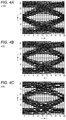
- FIGS. 4A, 4B, and 4C show results of acquiring the signal waveform data by n times of sampling using a 3-bit, 8-pattern pattern filter.
- Each figure is an example in which a resolution (number of cells) of the index It in the time direction is 20 and a resolution (number of cells) of the index Iv in the voltage direction is 32, and the number of processing data is 8 ⁇ n ⁇ 20 ⁇ 32.
- the vertical axis indicates a voltage (v) and the horizontal axis indicates a time (t), and signal waveforms acquired by sampling n times are superimposed and shown.
- the signal waveform is represented by light and shade according to the frequency at which the signal appears.
- the cell with the high frequency of the signal appearance is represented in a darker color and the cell with the high frequency of the signal absence is represented in a lighter color, by sampling n times at the same cell position.
- FIGS. 5A and 5B are diagrams showing generation results of the waveform data for showing an effect of the present embodiment.
- FIG. 5A illustrates a signal waveform when more digital data “0” is included in the received signal.
- the light and shade of the cell portion showing the waveform should be different at upper and lower sides sandwiching the opening of the eye pattern of the signal waveform, but a dark waveform is also displayed above the opening of the eye pattern, which indicates a possibility that display of the correct signal waveform corresponding to the received signal may not be obtained.
- the present embodiment while minimizing an increase in a load applied to the input signal to the data sampler 13 , it is possible to remove the inter-symbol interference between the cells even in an input signal whose periodicity is not stable and to display a clear waveform.
- the waveform data is generated by performing post-processing using probability distribution for each data pattern of continuous X bits, for example, 3 bits, for each cell of the waveform display range.
- a load of statistical operation which waveform processing unit 15 performs can be kept low.
- a configuration was provided such that it is prepared for the case where the appearance frequency of the bit pattern in the received signal is significantly biased to one side, the appearance frequency of the pattern data is calculated from the part of the received signal, and the upper limit is set when the result of the comparison and determination with the pattern data is counted.
- the appearance frequency of the bit pattern of the digital data “1” and “0” extracted from the received signal is biased, it is possible to display the correct signal waveform corresponding to the received signal.
- the present embodiment has shown the case of processing the received signal which differentially operates between two lines in the physical layer of the serial interface of the PCIe (registered trademark) standard, the present embodiment is not limited thereto, and it is possible to apply the present embodiment even to a single operation in a similar manner.
Landscapes
- Engineering & Computer Science (AREA)
- Computer Networks & Wireless Communication (AREA)
- Signal Processing (AREA)
- Power Engineering (AREA)
- Physics & Mathematics (AREA)
- Spectroscopy & Molecular Physics (AREA)
- Dc Digital Transmission (AREA)
Abstract
Description
Claims (10)
Applications Claiming Priority (3)
| Application Number | Priority Date | Filing Date | Title |
|---|---|---|---|
| JP2019-050640 | 2019-03-19 | ||
| JPJP2019-050640 | 2019-03-19 | ||
| JP2019050640A JP2020155848A (en) | 2019-03-19 | 2019-03-19 | Receiver and receiving method |
Publications (2)
| Publication Number | Publication Date |
|---|---|
| US20200304350A1 US20200304350A1 (en) | 2020-09-24 |
| US11070402B2 true US11070402B2 (en) | 2021-07-20 |
Family
ID=72514697
Family Applications (1)
| Application Number | Title | Priority Date | Filing Date |
|---|---|---|---|
| US16/555,434 Active US11070402B2 (en) | 2019-03-19 | 2019-08-29 | Receiving apparatus and receiving method |
Country Status (2)
| Country | Link |
|---|---|
| US (1) | US11070402B2 (en) |
| JP (1) | JP2020155848A (en) |
Families Citing this family (2)
| Publication number | Priority date | Publication date | Assignee | Title |
|---|---|---|---|---|
| JP7707006B2 (en) | 2021-09-21 | 2025-07-14 | キオクシア株式会社 | Receiving device and memory system |
| CN113868064B (en) * | 2021-09-30 | 2024-09-24 | 深圳忆联信息系统有限公司 | Method, device, computer equipment and storage medium for automatically measuring PCIE eye diagram |
Citations (11)
| Publication number | Priority date | Publication date | Assignee | Title |
|---|---|---|---|---|
| US6374388B1 (en) * | 1999-09-10 | 2002-04-16 | Agilent Technologies, Inc. | Equivalent time capture scheme for bit patterns within high data rate signals |
| US20020196055A1 (en) * | 2001-06-22 | 2002-12-26 | Jungerman Roger L. | Quasi-periodic optical sampling |
| US20040017366A1 (en) * | 2001-01-30 | 2004-01-29 | Iwatsu Electric Co., Ltd. | Waveform information display apparatus |
| US20060020412A1 (en) | 2004-07-23 | 2006-01-26 | Bruensteiner Matthew M | Analog waveform information from binary sampled measurements |
| US20070121714A1 (en) * | 2005-11-14 | 2007-05-31 | Baker Daniel G | Flexible timebase for EYE diagram |
| US20070229055A1 (en) | 2006-03-31 | 2007-10-04 | Kabushiki Kaisha Toshiba | Digital oscilloscope and method for displaying signal |
| US8860477B2 (en) | 2012-12-12 | 2014-10-14 | Fujitsu Limited | Receiver circuit |
| US20160006589A1 (en) * | 2014-07-01 | 2016-01-07 | Samsung Display Co., Ltd. | System and method of link optimization |
| US9401189B1 (en) * | 2013-03-15 | 2016-07-26 | Altera Corporation | Methods and apparatus for performing runtime data eye monitoring and continuous data strobe calibration |
| US20180059156A1 (en) * | 2016-08-25 | 2018-03-01 | Intel Corporation | Apparatus and method for calibrating high speed serial receiver analog front end and phase detector |
| US20190227103A1 (en) * | 2018-01-24 | 2019-07-25 | Anritsu Corporation | Sampling oscilloscope, trigger generation method, and sampling method |
-
2019
- 2019-03-19 JP JP2019050640A patent/JP2020155848A/en active Pending
- 2019-08-29 US US16/555,434 patent/US11070402B2/en active Active
Patent Citations (11)
| Publication number | Priority date | Publication date | Assignee | Title |
|---|---|---|---|---|
| US6374388B1 (en) * | 1999-09-10 | 2002-04-16 | Agilent Technologies, Inc. | Equivalent time capture scheme for bit patterns within high data rate signals |
| US20040017366A1 (en) * | 2001-01-30 | 2004-01-29 | Iwatsu Electric Co., Ltd. | Waveform information display apparatus |
| US20020196055A1 (en) * | 2001-06-22 | 2002-12-26 | Jungerman Roger L. | Quasi-periodic optical sampling |
| US20060020412A1 (en) | 2004-07-23 | 2006-01-26 | Bruensteiner Matthew M | Analog waveform information from binary sampled measurements |
| US20070121714A1 (en) * | 2005-11-14 | 2007-05-31 | Baker Daniel G | Flexible timebase for EYE diagram |
| US20070229055A1 (en) | 2006-03-31 | 2007-10-04 | Kabushiki Kaisha Toshiba | Digital oscilloscope and method for displaying signal |
| US8860477B2 (en) | 2012-12-12 | 2014-10-14 | Fujitsu Limited | Receiver circuit |
| US9401189B1 (en) * | 2013-03-15 | 2016-07-26 | Altera Corporation | Methods and apparatus for performing runtime data eye monitoring and continuous data strobe calibration |
| US20160006589A1 (en) * | 2014-07-01 | 2016-01-07 | Samsung Display Co., Ltd. | System and method of link optimization |
| US20180059156A1 (en) * | 2016-08-25 | 2018-03-01 | Intel Corporation | Apparatus and method for calibrating high speed serial receiver analog front end and phase detector |
| US20190227103A1 (en) * | 2018-01-24 | 2019-07-25 | Anritsu Corporation | Sampling oscilloscope, trigger generation method, and sampling method |
Non-Patent Citations (1)
| Title |
|---|
| Sandeep Krishnan, "A 10Gbps Eye Opening Monitor in 65nm CMOS", Published 2015 in 2015 IEEE International Symposium on Circuits and Systems (ISCAS), DOI:10.1109/ISCAS.2015.7169325, pp. 3028-3031. |
Also Published As
| Publication number | Publication date |
|---|---|
| US20200304350A1 (en) | 2020-09-24 |
| JP2020155848A (en) | 2020-09-24 |
Similar Documents
| Publication | Publication Date | Title |
|---|---|---|
| US11070402B2 (en) | Receiving apparatus and receiving method | |
| JPH10510939A (en) | Histogram equalization apparatus and method for improving contrast of moving image | |
| US10319113B2 (en) | Method for recovering highlights and saturated regions and extending dynamic range in a digital image | |
| US9299011B2 (en) | Signal processing apparatus, signal processing method, output apparatus, output method, and program for learning and restoring signals with sparse coefficients | |
| US10476716B2 (en) | PAM-n jitter/noise decomposition analysis | |
| EP3712842B1 (en) | System and method for evaluating symbols | |
| CN113538223B (en) | Noise image generation method, device, electronic device and storage medium | |
| JP5914843B2 (en) | Image processing apparatus and image processing method | |
| US5790200A (en) | Horizontal synchronization signal stabilization method and apparatus | |
| CN112637510A (en) | Scene self-adaptive image gain adjusting method, system and device and electronic equipment | |
| CN121239196A (en) | Clock duty cycle calibration methods, equipment, media, and procedures. | |
| US7359567B2 (en) | Signal processing apparatus for eliminating ringing signal and method thereof, record medium, and program | |
| US9100094B2 (en) | System and method for tuning a serial link | |
| US11468269B2 (en) | Arithmetic device, arithmetic method, and discrimination system | |
| CN119624842A (en) | A method, device and storage medium for image brightness correction | |
| CN112422941A (en) | Gamma adjustment method and device for display, electronic equipment and storage medium | |
| JP2024036374A (en) | Information processing device, information processing method, and program | |
| CN116363010A (en) | Image processing method and device | |
| US7576894B2 (en) | Device and method for sharpening image signal | |
| TWI689893B (en) | Background model updating method and related device | |
| EP3996032B1 (en) | Image processing with reduced latency and improved local processing | |
| CN121417866B (en) | An eye diagram calibration method and system | |
| CN111553317B (en) | Anti-fake code acquisition method and device, computer equipment and storage medium | |
| CN103685867A (en) | Backlight compensation method and device | |
| WO2024134885A1 (en) | Information processing device, information processing method, and recording medium |
Legal Events
| Date | Code | Title | Description |
|---|---|---|---|
| AS | Assignment |
Owner name: TOSHIBA MEMORY CORPORATION, JAPAN Free format text: ASSIGNMENT OF ASSIGNORS INTEREST;ASSIGNOR:YAMAMOTO, TAKAYA;REEL/FRAME:050213/0953 Effective date: 20190829 |
|
| FEPP | Fee payment procedure |
Free format text: ENTITY STATUS SET TO UNDISCOUNTED (ORIGINAL EVENT CODE: BIG.); ENTITY STATUS OF PATENT OWNER: LARGE ENTITY |
|
| STPP | Information on status: patent application and granting procedure in general |
Free format text: FINAL REJECTION MAILED |
|
| STPP | Information on status: patent application and granting procedure in general |
Free format text: DOCKETED NEW CASE - READY FOR EXAMINATION |
|
| STPP | Information on status: patent application and granting procedure in general |
Free format text: NOTICE OF ALLOWANCE MAILED -- APPLICATION RECEIVED IN OFFICE OF PUBLICATIONS |
|
| STPP | Information on status: patent application and granting procedure in general |
Free format text: PUBLICATIONS -- ISSUE FEE PAYMENT RECEIVED |
|
| STPP | Information on status: patent application and granting procedure in general |
Free format text: PUBLICATIONS -- ISSUE FEE PAYMENT VERIFIED |
|
| STCF | Information on status: patent grant |
Free format text: PATENTED CASE |
|
| AS | Assignment |
Owner name: KIOXIA CORPORATION, JAPAN Free format text: CHANGE OF NAME AND ADDRESS;ASSIGNOR:TOSHIBA MEMORY CORPORATION;REEL/FRAME:058905/0582 Effective date: 20191001 |
|
| MAFP | Maintenance fee payment |
Free format text: PAYMENT OF MAINTENANCE FEE, 4TH YEAR, LARGE ENTITY (ORIGINAL EVENT CODE: M1551); ENTITY STATUS OF PATENT OWNER: LARGE ENTITY Year of fee payment: 4 |