US11069738B2 - Infrared detector and infrared sensor including the same - Google Patents
Infrared detector and infrared sensor including the same Download PDFInfo
- Publication number
- US11069738B2 US11069738B2 US16/384,014 US201916384014A US11069738B2 US 11069738 B2 US11069738 B2 US 11069738B2 US 201916384014 A US201916384014 A US 201916384014A US 11069738 B2 US11069738 B2 US 11069738B2
- Authority
- US
- United States
- Prior art keywords
- infrared
- electrode
- semiconductor layer
- component
- infrared detector
- Prior art date
- Legal status (The legal status is an assumption and is not a legal conclusion. Google has not performed a legal analysis and makes no representation as to the accuracy of the status listed.)
- Active
Links
- 239000004065 semiconductor Substances 0.000 claims abstract description 111
- 239000002096 quantum dot Substances 0.000 claims abstract description 80
- 239000000758 substrate Substances 0.000 claims description 21
- 239000012535 impurity Substances 0.000 claims description 15
- 150000001875 compounds Chemical class 0.000 claims description 7
- 239000010410 layer Substances 0.000 description 203
- 238000005253 cladding Methods 0.000 description 39
- 239000000463 material Substances 0.000 description 36
- 229910001218 Gallium arsenide Inorganic materials 0.000 description 16
- 229910000530 Gallium indium arsenide Inorganic materials 0.000 description 11
- 229910000673 Indium arsenide Inorganic materials 0.000 description 11
- RPQDHPTXJYYUPQ-UHFFFAOYSA-N indium arsenide Chemical compound [In]#[As] RPQDHPTXJYYUPQ-UHFFFAOYSA-N 0.000 description 11
- -1 poly(3,4-ethylenedioxythiophene) Polymers 0.000 description 7
- 229910000980 Aluminium gallium arsenide Inorganic materials 0.000 description 4
- 239000004020 conductor Substances 0.000 description 4
- 239000013078 crystal Substances 0.000 description 4
- 238000010586 diagram Methods 0.000 description 4
- 230000031700 light absorption Effects 0.000 description 4
- 239000007769 metal material Substances 0.000 description 4
- 239000002159 nanocrystal Substances 0.000 description 4
- 229920001609 Poly(3,4-ethylenedioxythiophene) Polymers 0.000 description 3
- 238000000034 method Methods 0.000 description 3
- 229920000301 poly(3-hexylthiophene-2,5-diyl) polymer Polymers 0.000 description 3
- 229920000128 polypyrrole Polymers 0.000 description 3
- 239000000126 substance Substances 0.000 description 3
- 239000010409 thin film Substances 0.000 description 3
- XLYOFNOQVPJJNP-UHFFFAOYSA-N water Substances O XLYOFNOQVPJJNP-UHFFFAOYSA-N 0.000 description 3
- OKTJSMMVPCPJKN-UHFFFAOYSA-N Carbon Chemical compound [C] OKTJSMMVPCPJKN-UHFFFAOYSA-N 0.000 description 2
- 239000000853 adhesive Substances 0.000 description 2
- 230000001070 adhesive effect Effects 0.000 description 2
- 239000002717 carbon nanostructure Substances 0.000 description 2
- 229920001940 conductive polymer Polymers 0.000 description 2
- 238000001514 detection method Methods 0.000 description 2
- 239000006185 dispersion Substances 0.000 description 2
- 229910052737 gold Inorganic materials 0.000 description 2
- 229910021389 graphene Inorganic materials 0.000 description 2
- 229910021478 group 5 element Inorganic materials 0.000 description 2
- 229910052751 metal Inorganic materials 0.000 description 2
- 239000002184 metal Substances 0.000 description 2
- 239000002082 metal nanoparticle Substances 0.000 description 2
- 229910044991 metal oxide Inorganic materials 0.000 description 2
- 150000004706 metal oxides Chemical class 0.000 description 2
- 229910052709 silver Inorganic materials 0.000 description 2
- 239000002356 single layer Substances 0.000 description 2
- 241000764773 Inna Species 0.000 description 1
- 230000015572 biosynthetic process Effects 0.000 description 1
- 239000002041 carbon nanotube Substances 0.000 description 1
- 238000005229 chemical vapour deposition Methods 0.000 description 1
- 239000012792 core layer Substances 0.000 description 1
- 230000007123 defense Effects 0.000 description 1
- 238000000151 deposition Methods 0.000 description 1
- 230000000694 effects Effects 0.000 description 1
- 230000014509 gene expression Effects 0.000 description 1
- 229910052738 indium Inorganic materials 0.000 description 1
- APFVFJFRJDLVQX-UHFFFAOYSA-N indium atom Chemical compound [In] APFVFJFRJDLVQX-UHFFFAOYSA-N 0.000 description 1
- AMGQUBHHOARCQH-UHFFFAOYSA-N indium;oxotin Chemical compound [In].[Sn]=O AMGQUBHHOARCQH-UHFFFAOYSA-N 0.000 description 1
- 239000011777 magnesium Substances 0.000 description 1
- 238000004519 manufacturing process Methods 0.000 description 1
- 238000001451 molecular beam epitaxy Methods 0.000 description 1
- 239000003960 organic solvent Substances 0.000 description 1
- 239000002243 precursor Substances 0.000 description 1
- 239000004054 semiconductor nanocrystal Substances 0.000 description 1
- 230000035945 sensitivity Effects 0.000 description 1
- 238000002834 transmittance Methods 0.000 description 1
- 239000012780 transparent material Substances 0.000 description 1
- 238000007740 vapor deposition Methods 0.000 description 1
- 239000011701 zinc Substances 0.000 description 1
- 229910052725 zinc Inorganic materials 0.000 description 1
- YVTHLONGBIQYBO-UHFFFAOYSA-N zinc indium(3+) oxygen(2-) Chemical compound [O--].[Zn++].[In+3] YVTHLONGBIQYBO-UHFFFAOYSA-N 0.000 description 1
Images
Classifications
-
- H—ELECTRICITY
- H01—ELECTRIC ELEMENTS
- H01L—SEMICONDUCTOR DEVICES NOT COVERED BY CLASS H10
- H01L31/00—Semiconductor devices sensitive to infrared radiation, light, electromagnetic radiation of shorter wavelength or corpuscular radiation and specially adapted either for the conversion of the energy of such radiation into electrical energy or for the control of electrical energy by such radiation; Processes or apparatus specially adapted for the manufacture or treatment thereof or of parts thereof; Details thereof
- H01L31/08—Semiconductor devices sensitive to infrared radiation, light, electromagnetic radiation of shorter wavelength or corpuscular radiation and specially adapted either for the conversion of the energy of such radiation into electrical energy or for the control of electrical energy by such radiation; Processes or apparatus specially adapted for the manufacture or treatment thereof or of parts thereof; Details thereof in which radiation controls flow of current through the device, e.g. photoresistors
- H01L31/10—Semiconductor devices sensitive to infrared radiation, light, electromagnetic radiation of shorter wavelength or corpuscular radiation and specially adapted either for the conversion of the energy of such radiation into electrical energy or for the control of electrical energy by such radiation; Processes or apparatus specially adapted for the manufacture or treatment thereof or of parts thereof; Details thereof in which radiation controls flow of current through the device, e.g. photoresistors characterised by potential barriers, e.g. phototransistors
- H01L31/101—Devices sensitive to infrared, visible or ultraviolet radiation
-
- H—ELECTRICITY
- H01—ELECTRIC ELEMENTS
- H01L—SEMICONDUCTOR DEVICES NOT COVERED BY CLASS H10
- H01L27/00—Devices consisting of a plurality of semiconductor or other solid-state components formed in or on a common substrate
- H01L27/14—Devices consisting of a plurality of semiconductor or other solid-state components formed in or on a common substrate including semiconductor components sensitive to infrared radiation, light, electromagnetic radiation of shorter wavelength or corpuscular radiation and specially adapted either for the conversion of the energy of such radiation into electrical energy or for the control of electrical energy by such radiation
- H01L27/144—Devices controlled by radiation
- H01L27/146—Imager structures
- H01L27/14643—Photodiode arrays; MOS imagers
- H01L27/14649—Infrared imagers
-
- A—HUMAN NECESSITIES
- A61—MEDICAL OR VETERINARY SCIENCE; HYGIENE
- A61B—DIAGNOSIS; SURGERY; IDENTIFICATION
- A61B5/00—Measuring for diagnostic purposes; Identification of persons
- A61B5/44—Detecting, measuring or recording for evaluating the integumentary system, e.g. skin, hair or nails
- A61B5/441—Skin evaluation, e.g. for skin disorder diagnosis
- A61B5/443—Evaluating skin constituents, e.g. elastin, melanin, water
-
- B—PERFORMING OPERATIONS; TRANSPORTING
- B82—NANOTECHNOLOGY
- B82Y—SPECIFIC USES OR APPLICATIONS OF NANOSTRUCTURES; MEASUREMENT OR ANALYSIS OF NANOSTRUCTURES; MANUFACTURE OR TREATMENT OF NANOSTRUCTURES
- B82Y20/00—Nanooptics, e.g. quantum optics or photonic crystals
-
- G—PHYSICS
- G01—MEASURING; TESTING
- G01J—MEASUREMENT OF INTENSITY, VELOCITY, SPECTRAL CONTENT, POLARISATION, PHASE OR PULSE CHARACTERISTICS OF INFRARED, VISIBLE OR ULTRAVIOLET LIGHT; COLORIMETRY; RADIATION PYROMETRY
- G01J1/00—Photometry, e.g. photographic exposure meter
- G01J1/42—Photometry, e.g. photographic exposure meter using electric radiation detectors
- G01J1/44—Electric circuits
-
- G—PHYSICS
- G01—MEASURING; TESTING
- G01J—MEASUREMENT OF INTENSITY, VELOCITY, SPECTRAL CONTENT, POLARISATION, PHASE OR PULSE CHARACTERISTICS OF INFRARED, VISIBLE OR ULTRAVIOLET LIGHT; COLORIMETRY; RADIATION PYROMETRY
- G01J5/00—Radiation pyrometry, e.g. infrared or optical thermometry
- G01J5/02—Constructional details
- G01J5/0225—Shape of the cavity itself or of elements contained in or suspended over the cavity
- G01J5/024—Special manufacturing steps or sacrificial layers or layer structures
-
- G—PHYSICS
- G01—MEASURING; TESTING
- G01J—MEASUREMENT OF INTENSITY, VELOCITY, SPECTRAL CONTENT, POLARISATION, PHASE OR PULSE CHARACTERISTICS OF INFRARED, VISIBLE OR ULTRAVIOLET LIGHT; COLORIMETRY; RADIATION PYROMETRY
- G01J5/00—Radiation pyrometry, e.g. infrared or optical thermometry
- G01J5/02—Constructional details
- G01J5/04—Casings
- G01J5/046—Materials; Selection of thermal materials
-
- G—PHYSICS
- G01—MEASURING; TESTING
- G01J—MEASUREMENT OF INTENSITY, VELOCITY, SPECTRAL CONTENT, POLARISATION, PHASE OR PULSE CHARACTERISTICS OF INFRARED, VISIBLE OR ULTRAVIOLET LIGHT; COLORIMETRY; RADIATION PYROMETRY
- G01J5/00—Radiation pyrometry, e.g. infrared or optical thermometry
- G01J5/02—Constructional details
- G01J5/08—Optical arrangements
- G01J5/0853—Optical arrangements having infrared absorbers other than the usual absorber layers deposited on infrared detectors like bolometers, wherein the heat propagation between the absorber and the detecting element occurs within a solid
-
- G—PHYSICS
- G01—MEASURING; TESTING
- G01N—INVESTIGATING OR ANALYSING MATERIALS BY DETERMINING THEIR CHEMICAL OR PHYSICAL PROPERTIES
- G01N21/00—Investigating or analysing materials by the use of optical means, i.e. using sub-millimetre waves, infrared, visible or ultraviolet light
- G01N21/17—Systems in which incident light is modified in accordance with the properties of the material investigated
- G01N21/25—Colour; Spectral properties, i.e. comparison of effect of material on the light at two or more different wavelengths or wavelength bands
- G01N21/31—Investigating relative effect of material at wavelengths characteristic of specific elements or molecules, e.g. atomic absorption spectrometry
- G01N21/35—Investigating relative effect of material at wavelengths characteristic of specific elements or molecules, e.g. atomic absorption spectrometry using infrared light
- G01N21/3554—Investigating relative effect of material at wavelengths characteristic of specific elements or molecules, e.g. atomic absorption spectrometry using infrared light for determining moisture content
-
- H—ELECTRICITY
- H01—ELECTRIC ELEMENTS
- H01L—SEMICONDUCTOR DEVICES NOT COVERED BY CLASS H10
- H01L27/00—Devices consisting of a plurality of semiconductor or other solid-state components formed in or on a common substrate
- H01L27/14—Devices consisting of a plurality of semiconductor or other solid-state components formed in or on a common substrate including semiconductor components sensitive to infrared radiation, light, electromagnetic radiation of shorter wavelength or corpuscular radiation and specially adapted either for the conversion of the energy of such radiation into electrical energy or for the control of electrical energy by such radiation
- H01L27/144—Devices controlled by radiation
- H01L27/146—Imager structures
- H01L27/14665—Imagers using a photoconductor layer
- H01L27/14669—Infrared imagers
-
- H—ELECTRICITY
- H01—ELECTRIC ELEMENTS
- H01L—SEMICONDUCTOR DEVICES NOT COVERED BY CLASS H10
- H01L27/00—Devices consisting of a plurality of semiconductor or other solid-state components formed in or on a common substrate
- H01L27/14—Devices consisting of a plurality of semiconductor or other solid-state components formed in or on a common substrate including semiconductor components sensitive to infrared radiation, light, electromagnetic radiation of shorter wavelength or corpuscular radiation and specially adapted either for the conversion of the energy of such radiation into electrical energy or for the control of electrical energy by such radiation
- H01L27/144—Devices controlled by radiation
- H01L27/146—Imager structures
- H01L27/14683—Processes or apparatus peculiar to the manufacture or treatment of these devices or parts thereof
- H01L27/14694—The active layers comprising only AIIIBV compounds, e.g. GaAs, InP
-
- H—ELECTRICITY
- H01—ELECTRIC ELEMENTS
- H01L—SEMICONDUCTOR DEVICES NOT COVERED BY CLASS H10
- H01L31/00—Semiconductor devices sensitive to infrared radiation, light, electromagnetic radiation of shorter wavelength or corpuscular radiation and specially adapted either for the conversion of the energy of such radiation into electrical energy or for the control of electrical energy by such radiation; Processes or apparatus specially adapted for the manufacture or treatment thereof or of parts thereof; Details thereof
- H01L31/02—Details
- H01L31/0224—Electrodes
- H01L31/022466—Electrodes made of transparent conductive layers, e.g. TCO, ITO layers
-
- H—ELECTRICITY
- H01—ELECTRIC ELEMENTS
- H01L—SEMICONDUCTOR DEVICES NOT COVERED BY CLASS H10
- H01L31/00—Semiconductor devices sensitive to infrared radiation, light, electromagnetic radiation of shorter wavelength or corpuscular radiation and specially adapted either for the conversion of the energy of such radiation into electrical energy or for the control of electrical energy by such radiation; Processes or apparatus specially adapted for the manufacture or treatment thereof or of parts thereof; Details thereof
- H01L31/0248—Semiconductor devices sensitive to infrared radiation, light, electromagnetic radiation of shorter wavelength or corpuscular radiation and specially adapted either for the conversion of the energy of such radiation into electrical energy or for the control of electrical energy by such radiation; Processes or apparatus specially adapted for the manufacture or treatment thereof or of parts thereof; Details thereof characterised by their semiconductor bodies
- H01L31/0256—Semiconductor devices sensitive to infrared radiation, light, electromagnetic radiation of shorter wavelength or corpuscular radiation and specially adapted either for the conversion of the energy of such radiation into electrical energy or for the control of electrical energy by such radiation; Processes or apparatus specially adapted for the manufacture or treatment thereof or of parts thereof; Details thereof characterised by their semiconductor bodies characterised by the material
- H01L31/0264—Inorganic materials
- H01L31/0304—Inorganic materials including, apart from doping materials or other impurities, only AIIIBV compounds
- H01L31/03046—Inorganic materials including, apart from doping materials or other impurities, only AIIIBV compounds including ternary or quaternary compounds, e.g. GaAlAs, InGaAs, InGaAsP
-
- H—ELECTRICITY
- H01—ELECTRIC ELEMENTS
- H01L—SEMICONDUCTOR DEVICES NOT COVERED BY CLASS H10
- H01L31/00—Semiconductor devices sensitive to infrared radiation, light, electromagnetic radiation of shorter wavelength or corpuscular radiation and specially adapted either for the conversion of the energy of such radiation into electrical energy or for the control of electrical energy by such radiation; Processes or apparatus specially adapted for the manufacture or treatment thereof or of parts thereof; Details thereof
- H01L31/0248—Semiconductor devices sensitive to infrared radiation, light, electromagnetic radiation of shorter wavelength or corpuscular radiation and specially adapted either for the conversion of the energy of such radiation into electrical energy or for the control of electrical energy by such radiation; Processes or apparatus specially adapted for the manufacture or treatment thereof or of parts thereof; Details thereof characterised by their semiconductor bodies
- H01L31/0352—Semiconductor devices sensitive to infrared radiation, light, electromagnetic radiation of shorter wavelength or corpuscular radiation and specially adapted either for the conversion of the energy of such radiation into electrical energy or for the control of electrical energy by such radiation; Processes or apparatus specially adapted for the manufacture or treatment thereof or of parts thereof; Details thereof characterised by their semiconductor bodies characterised by their shape or by the shapes, relative sizes or disposition of the semiconductor regions
- H01L31/035209—Semiconductor devices sensitive to infrared radiation, light, electromagnetic radiation of shorter wavelength or corpuscular radiation and specially adapted either for the conversion of the energy of such radiation into electrical energy or for the control of electrical energy by such radiation; Processes or apparatus specially adapted for the manufacture or treatment thereof or of parts thereof; Details thereof characterised by their semiconductor bodies characterised by their shape or by the shapes, relative sizes or disposition of the semiconductor regions comprising a quantum structures
- H01L31/035218—Semiconductor devices sensitive to infrared radiation, light, electromagnetic radiation of shorter wavelength or corpuscular radiation and specially adapted either for the conversion of the energy of such radiation into electrical energy or for the control of electrical energy by such radiation; Processes or apparatus specially adapted for the manufacture or treatment thereof or of parts thereof; Details thereof characterised by their semiconductor bodies characterised by their shape or by the shapes, relative sizes or disposition of the semiconductor regions comprising a quantum structures the quantum structure being quantum dots
-
- H—ELECTRICITY
- H01—ELECTRIC ELEMENTS
- H01L—SEMICONDUCTOR DEVICES NOT COVERED BY CLASS H10
- H01L31/00—Semiconductor devices sensitive to infrared radiation, light, electromagnetic radiation of shorter wavelength or corpuscular radiation and specially adapted either for the conversion of the energy of such radiation into electrical energy or for the control of electrical energy by such radiation; Processes or apparatus specially adapted for the manufacture or treatment thereof or of parts thereof; Details thereof
- H01L31/0248—Semiconductor devices sensitive to infrared radiation, light, electromagnetic radiation of shorter wavelength or corpuscular radiation and specially adapted either for the conversion of the energy of such radiation into electrical energy or for the control of electrical energy by such radiation; Processes or apparatus specially adapted for the manufacture or treatment thereof or of parts thereof; Details thereof characterised by their semiconductor bodies
- H01L31/0352—Semiconductor devices sensitive to infrared radiation, light, electromagnetic radiation of shorter wavelength or corpuscular radiation and specially adapted either for the conversion of the energy of such radiation into electrical energy or for the control of electrical energy by such radiation; Processes or apparatus specially adapted for the manufacture or treatment thereof or of parts thereof; Details thereof characterised by their semiconductor bodies characterised by their shape or by the shapes, relative sizes or disposition of the semiconductor regions
- H01L31/035236—Superlattices; Multiple quantum well structures
-
- H—ELECTRICITY
- H01—ELECTRIC ELEMENTS
- H01L—SEMICONDUCTOR DEVICES NOT COVERED BY CLASS H10
- H01L31/00—Semiconductor devices sensitive to infrared radiation, light, electromagnetic radiation of shorter wavelength or corpuscular radiation and specially adapted either for the conversion of the energy of such radiation into electrical energy or for the control of electrical energy by such radiation; Processes or apparatus specially adapted for the manufacture or treatment thereof or of parts thereof; Details thereof
- H01L31/0248—Semiconductor devices sensitive to infrared radiation, light, electromagnetic radiation of shorter wavelength or corpuscular radiation and specially adapted either for the conversion of the energy of such radiation into electrical energy or for the control of electrical energy by such radiation; Processes or apparatus specially adapted for the manufacture or treatment thereof or of parts thereof; Details thereof characterised by their semiconductor bodies
- H01L31/036—Semiconductor devices sensitive to infrared radiation, light, electromagnetic radiation of shorter wavelength or corpuscular radiation and specially adapted either for the conversion of the energy of such radiation into electrical energy or for the control of electrical energy by such radiation; Processes or apparatus specially adapted for the manufacture or treatment thereof or of parts thereof; Details thereof characterised by their semiconductor bodies characterised by their crystalline structure or particular orientation of the crystalline planes
- H01L31/0384—Semiconductor devices sensitive to infrared radiation, light, electromagnetic radiation of shorter wavelength or corpuscular radiation and specially adapted either for the conversion of the energy of such radiation into electrical energy or for the control of electrical energy by such radiation; Processes or apparatus specially adapted for the manufacture or treatment thereof or of parts thereof; Details thereof characterised by their semiconductor bodies characterised by their crystalline structure or particular orientation of the crystalline planes including other non-monocrystalline materials, e.g. semiconductor particles embedded in an insulating material
- H01L31/03845—Semiconductor devices sensitive to infrared radiation, light, electromagnetic radiation of shorter wavelength or corpuscular radiation and specially adapted either for the conversion of the energy of such radiation into electrical energy or for the control of electrical energy by such radiation; Processes or apparatus specially adapted for the manufacture or treatment thereof or of parts thereof; Details thereof characterised by their semiconductor bodies characterised by their crystalline structure or particular orientation of the crystalline planes including other non-monocrystalline materials, e.g. semiconductor particles embedded in an insulating material comprising semiconductor nanoparticles embedded in a semiconductor matrix
-
- H—ELECTRICITY
- H01—ELECTRIC ELEMENTS
- H01L—SEMICONDUCTOR DEVICES NOT COVERED BY CLASS H10
- H01L31/00—Semiconductor devices sensitive to infrared radiation, light, electromagnetic radiation of shorter wavelength or corpuscular radiation and specially adapted either for the conversion of the energy of such radiation into electrical energy or for the control of electrical energy by such radiation; Processes or apparatus specially adapted for the manufacture or treatment thereof or of parts thereof; Details thereof
- H01L31/08—Semiconductor devices sensitive to infrared radiation, light, electromagnetic radiation of shorter wavelength or corpuscular radiation and specially adapted either for the conversion of the energy of such radiation into electrical energy or for the control of electrical energy by such radiation; Processes or apparatus specially adapted for the manufacture or treatment thereof or of parts thereof; Details thereof in which radiation controls flow of current through the device, e.g. photoresistors
- H01L31/10—Semiconductor devices sensitive to infrared radiation, light, electromagnetic radiation of shorter wavelength or corpuscular radiation and specially adapted either for the conversion of the energy of such radiation into electrical energy or for the control of electrical energy by such radiation; Processes or apparatus specially adapted for the manufacture or treatment thereof or of parts thereof; Details thereof in which radiation controls flow of current through the device, e.g. photoresistors characterised by potential barriers, e.g. phototransistors
- H01L31/101—Devices sensitive to infrared, visible or ultraviolet radiation
- H01L31/1013—Devices sensitive to infrared, visible or ultraviolet radiation devices sensitive to two or more wavelengths, e.g. multi-spectrum radiation detection devices
-
- H—ELECTRICITY
- H01—ELECTRIC ELEMENTS
- H01L—SEMICONDUCTOR DEVICES NOT COVERED BY CLASS H10
- H01L31/00—Semiconductor devices sensitive to infrared radiation, light, electromagnetic radiation of shorter wavelength or corpuscular radiation and specially adapted either for the conversion of the energy of such radiation into electrical energy or for the control of electrical energy by such radiation; Processes or apparatus specially adapted for the manufacture or treatment thereof or of parts thereof; Details thereof
- H01L31/08—Semiconductor devices sensitive to infrared radiation, light, electromagnetic radiation of shorter wavelength or corpuscular radiation and specially adapted either for the conversion of the energy of such radiation into electrical energy or for the control of electrical energy by such radiation; Processes or apparatus specially adapted for the manufacture or treatment thereof or of parts thereof; Details thereof in which radiation controls flow of current through the device, e.g. photoresistors
- H01L31/10—Semiconductor devices sensitive to infrared radiation, light, electromagnetic radiation of shorter wavelength or corpuscular radiation and specially adapted either for the conversion of the energy of such radiation into electrical energy or for the control of electrical energy by such radiation; Processes or apparatus specially adapted for the manufacture or treatment thereof or of parts thereof; Details thereof in which radiation controls flow of current through the device, e.g. photoresistors characterised by potential barriers, e.g. phototransistors
- H01L31/101—Devices sensitive to infrared, visible or ultraviolet radiation
- H01L31/102—Devices sensitive to infrared, visible or ultraviolet radiation characterised by only one potential barrier
- H01L31/105—Devices sensitive to infrared, visible or ultraviolet radiation characterised by only one potential barrier the potential barrier being of the PIN type
-
- H—ELECTRICITY
- H01—ELECTRIC ELEMENTS
- H01L—SEMICONDUCTOR DEVICES NOT COVERED BY CLASS H10
- H01L31/00—Semiconductor devices sensitive to infrared radiation, light, electromagnetic radiation of shorter wavelength or corpuscular radiation and specially adapted either for the conversion of the energy of such radiation into electrical energy or for the control of electrical energy by such radiation; Processes or apparatus specially adapted for the manufacture or treatment thereof or of parts thereof; Details thereof
- H01L31/08—Semiconductor devices sensitive to infrared radiation, light, electromagnetic radiation of shorter wavelength or corpuscular radiation and specially adapted either for the conversion of the energy of such radiation into electrical energy or for the control of electrical energy by such radiation; Processes or apparatus specially adapted for the manufacture or treatment thereof or of parts thereof; Details thereof in which radiation controls flow of current through the device, e.g. photoresistors
- H01L31/10—Semiconductor devices sensitive to infrared radiation, light, electromagnetic radiation of shorter wavelength or corpuscular radiation and specially adapted either for the conversion of the energy of such radiation into electrical energy or for the control of electrical energy by such radiation; Processes or apparatus specially adapted for the manufacture or treatment thereof or of parts thereof; Details thereof in which radiation controls flow of current through the device, e.g. photoresistors characterised by potential barriers, e.g. phototransistors
- H01L31/101—Devices sensitive to infrared, visible or ultraviolet radiation
- H01L31/102—Devices sensitive to infrared, visible or ultraviolet radiation characterised by only one potential barrier
- H01L31/109—Devices sensitive to infrared, visible or ultraviolet radiation characterised by only one potential barrier the potential barrier being of the PN heterojunction type
-
- G—PHYSICS
- G01—MEASURING; TESTING
- G01J—MEASUREMENT OF INTENSITY, VELOCITY, SPECTRAL CONTENT, POLARISATION, PHASE OR PULSE CHARACTERISTICS OF INFRARED, VISIBLE OR ULTRAVIOLET LIGHT; COLORIMETRY; RADIATION PYROMETRY
- G01J1/00—Photometry, e.g. photographic exposure meter
- G01J1/42—Photometry, e.g. photographic exposure meter using electric radiation detectors
- G01J1/44—Electric circuits
- G01J2001/4446—Type of detector
Definitions
- Apparatuses consistent with exemplary embodiments relate to infrared detectors, and more particularly, to infrared detectors capable of absorbing infrared light and infrared sensors including the infrared detectors.
- Infrared images may be generated by detecting infrared light emitted from objects by using infrared detectors. Infrared images are typically generated by light in wavelength regions that are not identifiable by the naked human eye. However, infrared cameras perform pixel detection using infrared detectors and perform analog and digital signal processing to generate images that can be seen by the human eye. These infrared images are used in various fields such as the defense industry, medical equipment, surveillance, and security.
- Infrared light is harmless to the human body and thus may be used for measuring biometric information of the human body, for example, a content of moisture and the like.
- an infrared detector uses a band pass filter to obtain information about the substance.
- a band pass filter it is difficult to miniaturize an infrared detector.
- One or more exemplary embodiments may provide infrared detectors and infrared sensors which absorb only infrared light in a specific wavelength band.
- One or more exemplary embodiments may provide are infrared detectors and infrared sensors which are not sensitive to temperature.
- an infrared detector includes: a substrate; a first electrode, disposed on the substrate; and an infrared-absorbing layer disposed on the first electrode, wherein the infrared-absorbing layer absorbs incident infrared light in a specific wavelength band and generates a current corresponding to absorbed infrared light; and, a second electrode disposed on the infrared-absorbing layer, wherein the at least one infrared-absorbing layer includes: a first semiconductor layer including a first component; a plurality of quantum dots, spaced apart from each other on the first semiconductor layer and including a second component different from the first component; and a second semiconductor layer including the first component and the second component and covering the plurality of quantum dots.
- the specific wavelength band may be determined by a content of the second component in the at least one infrared-absorbing layer.
- a center wavelength of the specific wavelength band may be proportional to a content of the second component.
- a center wavelength of the specific wavelength band may be 1 to 3 ⁇ m.
- An energy band of the second semiconductor layer may be between an energy band of the quantum dots and an energy band of the first semiconductor layer.
- the quantum dots may have a lower energy band than the first semiconductor layer and the second semiconductor layer.
- the substrate may include the first component.
- At least one of the first component and the second component may be a Group III element.
- the first semiconductor layer may include a compound comprising the first component and a third component different from the first component and the second component
- the second semiconductor layer may include a compound comprising the first component, the second component, and the third component
- the third component may be a Group V element.
- the at least one infrared-absorbing layer may include first and second infrared-absorbing layers arranged in a direction from the first electrode to the second electrode.
- the infrared detector may further include at least one of: a first cladding layer between the first electrode and the infrared-absorbing layer and having an energy band higher than an energy band of the infrared-absorbing layer; and a second cladding layer between the second electrode and the infrared-absorbing layer and having an energy band higher than the energy band of the infrared-absorbing layer.
- At least one of the first and second cladding layers may include a fourth component that is different from the first and second components.
- the fourth component may be a metal.
- the infrared detector may further include a third semiconductor layer between the at least one infrared-absorbing layer and the second electrode.
- the third semiconductor layer may include a same material as the first semiconductor layer.
- a sum of thicknesses of the at least one infrared-absorbing layer and the third semiconductor layer may be equal to or greater than a wavelength of the infrared light.
- the sum of the thicknesses of the at least one infrared-absorbing layer and the third semiconductor layer may be a multiple of the wavelength of the infrared light.
- One of the first electrode and the second electrode may include a semiconductor layer doped with n-type impurities and the other may include a semiconductor layer doped with p-type impurities.
- the second electrode may include a transparent electrode.
- the second electrode may overlap a portion of the infrared-absorbing layer, as viewed from an incident direction of the infrared light on the infrared detector.
- an infrared sensor includes a plurality of infrared detectors identical to the infrared detector and detecting infrared light reflected from a target object.
- the plurality of infrared detectors may include a first infrared detector and a second infrared detector, arranged in a direction perpendicular to an incident direction of light.
- the first infrared detector and the second infrared detector may absorb light of a same wavelength.
- a substrate of the first infrared detector and a substrate of the second infrared detector may together comprise a single layer common to the first infrared detector and the second infrared detector.
- a first electrode of the first infrared detector and a second electrode of the second infrared detector may be connected to each other by an electrode pad.
- the plurality of infrared detectors may include a third infrared detector and a fourth infrared detector, arranged in a direction parallel to an incident direction of light.
- the third infrared detector and the fourth infrared detector may absorb light having different wavelengths.
- FIG. 1 is a cross-sectional view schematically illustrating an infrared detector according to an exemplary embodiment
- FIG. 2 is a graph showing threshold currents of various crystal structures according to temperature
- FIG. 3A is a graph showing a wavelength band within which infrared light is absorbed by a bulk structure
- FIG. 3B is a graph showing a wavelength band within which infrared light is absorbed by quantum dots
- FIG. 4 is a graph showing the wavelength of infrared light absorbed by quantum dots according to an exemplary embodiment and the wavelength of infrared light absorbed by quantum dots doped with the material of a first semiconductor layer;
- FIG. 5 is a table showing a relationship between a center wavelength and the content of indium (In), according to an exemplary embodiment
- FIG. 6 is a diagram illustrating an energy band of an infrared-absorbing layer in an infrared detector according to an exemplary embodiment
- FIG. 7 is a cross-sectional view illustrating an infrared detector according to another exemplary embodiment
- FIG. 8 is a diagram illustrating energy bands of an infrared-absorbing layer and cladding layers of FIG. 7 ;
- FIG. 9 is a view illustrating an infrared sensor according to an exemplary embodiment
- FIG. 10 is a view illustrating an infrared sensor according to another exemplary embodiment
- FIG. 11 is a graph showing light absorption rates according to materials
- FIG. 12A shows a result obtained by photographing a plurality of sheets having different moisture content ratios with a general camera
- FIG. 12B shows a result obtained by photographing a plurality of sheets having different moisture content ratios with an infrared sensor.
- FIG. 1 is a cross-sectional view schematically illustrating an infrared detector 100 according to an exemplary embodiment.
- the infrared detector 100 may detect near infrared light, e.g., infrared light having a wavelength between about 750 nm and 3000 nm.
- the infrared detector 100 may include a substrate 10 , first and second electrodes 20 and 30 that are disposed on the substrate 10 and spaced apart from one another, and one or more infrared-absorbing layers 40 disposed between the first and second electrodes 20 and 30 and which absorb infrared light in a specific wavelength band to generate a current.
- the infrared detector 100 may include a Group III-V semiconductor material. By forming layers of the infrared detector 100 with materials having similar lattice constants, it is easily possible to stack the layers and miniaturize the infrared detector 100 .
- the substrate 10 may include a Group III-V semiconductor material, and may include the same material as some layers of the infrared-absorbing layer 40 described below.
- the substrate 10 may include GaAs.
- the first and second electrodes 20 and 30 may include a conductive material, e.g., a metal material or a conductive oxide.
- the first and second electrodes 20 and 30 may include a transparent conductive material.
- the first and second electrodes 20 and 30 may include a metal oxide such as indium tin oxide (ITO) or indium zinc oxide (IZO), a metal nanoparticle dispersion thin film such as Au or Ag, a carbon nanostructure such as carbon nanotubes (CNTs) or graphene, or a conductive polymer such as poly(3,4-ethylenedioxythiophene) (PEDOT), polypyrrole (PPy), or poly(3-hexylthiophene) (P3HT).
- PEDOT poly(3,4-ethylenedioxythiophene)
- PPy polypyrrole
- P3HT poly(3-hexylthiophene)
- the first and second electrodes 20 and 30 may include an impurity-doped semiconductor material.
- the first electrode 20 may be a semiconductor layer doped with impurities of a first type and may include a Group III-V semiconductor material.
- the first electrode 20 may include GaAs doped with n-type impurities such as Si, Ge, Se, or Te.
- the second electrode 30 may be a semiconductor layer doped with impurities of a second type and may include a Group III-V semiconductor material.
- the second electrode 30 may include GaAs doped with p-type impurities.
- Mg, Zn, Be or the like may be used as the p-type impurities.
- the infrared-absorbing layer 40 may absorb incident infrared light only within a specific wavelength band.
- infrared light When infrared light is incident on the infrared-absorbing layer 40 , electrons, that have absorbed the energy of an energy band gap corresponding to the infrared light, move, resulting in an imbalance of electrons and holes, and a current is generated in accordance with the imbalance of electrons and holes.
- the current may flow from the first electrode 20 to the second electrode 30 or from the second electrode 30 to the first electrode 20 through the infrared-absorbing layer 40 .
- the infrared-absorbing layer 40 may also include a Group III-V semiconductor material.
- the infrared-absorbing layer 40 may include a first semiconductor layer 42 , a plurality of quantum dots 44 that are spaced apart from each other on the first semiconductor layer 42 , and a second semiconductor layer 46 covering the plurality of quantum dots 44 .
- the first semiconductor layer 42 may include a first component including a Group III element.
- the first semiconductor layer 42 may include a Group III-V semiconductor material.
- the first semiconductor layer 42 may include a material having the highest energy band of the infrared-absorbing layer 40 .
- the first semiconductor layer 42 may include GaAs.
- the first semiconductor layer 42 may determine a wavelength band within which infrared light is absorbed by the infrared-absorbing layer 40 .
- the plurality of quantum dots 44 may be arranged on the first semiconductor layer 42 . Each of the plurality of quantum dots 44 may directly contact the first semiconductor layer 42 . The plurality of quantum dots 44 may be randomly arranged.
- the quantum dots 44 may be nanocrystals of a semiconductor material having a diameter of about 10 nm or less.
- a vapor deposition method such as metal organic chemical vapor deposition (MOCVD) or molecular beam epitaxy (MBE), a chemical wet method in which a precursor material is added to an organic solvent to grow crystals, or the like may be used.
- the quantum dots 44 may include a second component including a Group III element.
- the quantum dots 44 may be nanocrystals of a Group III-V compound semiconductor.
- the Group III-V compound semiconductor nanocrystal may be any one selected from the group consisting of GaN, GaP, GaAs, AN, AlP, AlAs, InN, InP, InAs, GaNP, GaNAs, GaPAs, AlNP, AlNAs, AlPAs, InNP, InNAs, InPAs, GaAlNP, GaAlNAs, GaAlPAs, GaInNP, GaInNAs, GaInPAs, InAlNP, InAlNAs, and InAlPAs.
- the quantum dots 44 may include InAs having a similar lattice constant.
- the nanosize quantum dots 44 exhibit a quantum confinement effect, such that a bandgap becomes larger and the bandgap has a discontinuous bandgap structure like one individual atom, unlike a bulk structure.
- the quantum dots 44 are not limited to a specific structure but may have a single structure including only a core or may have any one selected from a core-single shell structure including a shell having a core and a single layer and a core-multiple shell structure including a shell having a core and multiple layers.
- FIG. 2 is a graph showing threshold currents of various crystal structures according to temperature.
- a bulk structure has a large change in a threshold current according to temperature.
- the infrared detector may require a cooler to maintain a constant temperature.
- the quantum dots 44 do not require a cooler because the threshold current of the quantum dots 44 is almost constant according to temperature.
- the quantum dots 44 may serve as seeds in depositing materials having different lattice constants to facilitate formation of layers including the materials.
- the quantum dots 44 may serve as an adhesive.
- the quantum dots 44 may be sensitive to light in a specific wavelength band.
- FIG. 3A is a graph showing a wavelength band within which infrared light is absorbed by a bulk structure
- FIG. 3B is a graph showing a wavelength band within which infrared light is absorbed by quantum dots.
- the bulk structure used to obtain the graph of FIG. 3A includes InGaAs
- the quantum dots used to obtain the graph of FIG. 3B include InAs.
- the bulk structure absorbs infrared light in a wide wavelength band.
- the width of a wavelength band within which the responsivity of the infrared light absorbed by the bulk structure is about 0.4 or more is about 750 nm.
- the quantum dots absorb infrared light within a narrow wavelength band.
- the width of the wavelength band within which the responsivity of the infrared ray absorbed by the quantum dots is about 0.4 or more is about 50 nm.
- An infrared detector including a bulk structure includes a bandpass filter as a component to determine whether the infrared detector absorbs infrared light in a particular wavelength band.
- a bandpass filter as a component to determine whether the infrared detector absorbs infrared light in a particular wavelength band.
- an infrared detector including quantum dots has a narrow wavelength band within which infrared light is detected, and thus need not include a separate band filter. Thus, the structure of the infrared detector including the quantum dots may be simplified.
- the infrared-absorbing layer 40 may include the second semiconductor layer 46 covering the plurality of quantum dots 44 .
- the second semiconductor layer 46 may include a material having an energy band that is greater than that of the quantum dots 44 .
- the energy band of the second semiconductor layer 46 may be greater than the energy band of the quantum dots 44 and may be less than the energy band of the first semiconductor layer 42 .
- the second semiconductor layer 46 may include a second component contained in the quantum dots 44 and a second component including a Group III element, which is different from the second component contained in the quantum dots 44 .
- the quantum dots 44 include InAs
- the second semiconductor layer 46 may include InGaAs.
- the first semiconductor layer 42 , the plurality of quantum dots 44 , and the second semiconductor layer 46 may include the same component.
- Each of the first semiconductor layer 42 , the plurality of quantum dots 44 , and the second semiconductor layer 46 may include a third component including a Group V element.
- the first semiconductor layer 42 may include GaAs
- the quantum dots 44 may include InAs
- the second semiconductor layer 46 may include InGaAs.
- the infrared detector 100 may further include a third semiconductor layer 50 between the infrared-absorbing layer 40 and the second electrode 30 .
- the third semiconductor layer 50 may include the same material as the first semiconductor layer 42 .
- the third semiconductor layer 50 may also include GaAs.
- the upper surface of the infrared-absorbing layer 40 may be planarized so that a plurality of infrared-absorbing layers may be stacked.
- the quantum dots 44 have a crystal structure
- the second semiconductor layer 46 may have the form of a thin film and may cover the quantum dots 44 .
- the surface of the second semiconductor layer 46 may be curved by the quantum dots 44
- the infrared-absorbing layer 40 may be planarized by the stacking of the first semiconductor layer 42 .
- the infrared detector 100 may include one or more infrared-absorbing layers 40 .
- the one or more infrared-absorbing layers 40 may be arranged in a direction from the first electrode 20 to the second electrode 30 .
- the one or more infrared-absorbing layers 40 may include a first infrared-absorbing layer 40 a , disposed on and in contact with the first electrode 20 , a second infrared-absorbing layer 40 b , disposed below and in contact with the third semiconductor layer 50 , and a third infrared-absorbing layer 40 c arranged between the first infrared-absorbing layer 40 a and the second infrared-absorbing layer 40 b.
- the one or more infrared-absorbing layers 40 and the third semiconductor layer 50 may determine the content of In component contained in the infrared-absorbing layers 40 . Since the In component is contained in the quantum dots 44 and the second semiconductor layer 46 , the content of the In component may be adjusted by adjusting the thicknesses of the first semiconductor layer 42 and the third semiconductor layer 50 . For example, since the content of the Ga component increases as the thicknesses of the first semiconductor layer 42 and of the third semiconductor layer 50 increase, the content of the In component may be comparatively reduced. In the infrared detector 100 according to the present exemplary embodiment, the content of the In component may be determined so that infrared light having a center wavelength of about 1 to 3 ⁇ m is absorbed.
- the sum (t) of the thicknesses of the one or more infrared-absorbing layers 40 and the third semiconductor layer 50 may be greater than or equal to the wavelength of the infrared light to be detected.
- the sum of the thicknesses of the one or more infrared-absorbing layers 40 and the third semiconductor layer 50 may be a multiple of the wavelength of the infrared light to be detected.
- the infrared light to be detected may be stably incident on the infrared-absorbing layer 40 .
- FIG. 4 is a graph showing the wavelength of infrared light absorbed by quantum dots according to an exemplary embodiment and the wavelength of infrared light absorbed by quantum dots doped with a second semiconductor layer.
- quantum dots i.e., the quantum dots 44
- InAs react to infrared light having a center wavelength of about 1350 nm
- quantum dots doped with InGaAs react to infrared light having a center wavelength of about 1460 nm. That is, it may be seen that the degree of doping of InGaAs may change the wavelength band of infrared light to which quantum dots react.
- quantum dots including InAs and a responsivity of quantum dots doped with InGaAs may be 0.4 or more at the width of the wavelength band of about 50 nm.
- the detection sensitivity of infrared light may be maintained while adjusting a wavelength band to be detected by the doping of InGaAs.
- Equation 1 The band gap energy Eg(x) of InxGa1-xAs is expressed by Equation (1).
- Eg( x ) 1.425 eV ⁇ 1.501 x eV+0.436 x 2 eV [Equation 1]
- x is equal to or greater than 0 and is equal to or less than 10 (i.e., 0 ⁇ x ⁇ 10).
- the band gap energy Eg(x) changes depending on the content of In component.
- a change in the bandgap energy Eg(x) means that the wavelength of infrared light to be absorbed may be changed.
- FIG. 5 is a table showing a relationship between a center wavelength and the content of In component, according to an exemplary embodiment. As shown in FIG. 5 , it may be seen that the content of In component and a band gap energy are proportional to each other and the content of In component and the center wavelength of infrared light to be absorbed are inversely proportional to each other. Thus, the center wavelength of infrared light to be absorbed may be adjusted by controlling the content of In component.
- FIG. 6 is a diagram illustrating an energy band of the infrared-absorbing layer 40 in the infrared detector 100 according to the exemplary embodiment.
- the infrared-absorbing layer 40 may have an energy band as shown in FIG. 6 .
- electrons of the infrared-absorbing layer 40 absorb infrared light having a specific wavelength, for example, the wavelength of 1450 nm, the electrons are activated and move.
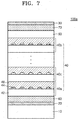
- FIG. 7 is a cross-sectional view illustrating an infrared detector 100 a according to another exemplary embodiment.
- the infrared detector 100 a of FIG. 7 may further include a first cladding layer 60 arranged between a first electrode 20 and an infrared-absorbing layer 40 and a second cladding layer 70 arranged between a second electrode 30 and the infrared-absorbing layer 40 .
- the first cladding layer 60 and the second cladding layer 70 may include a material having an energy band higher than the energy band of the infrared-absorbing layer 40 .
- the first cladding layer 60 and the second cladding layer 70 may include a metal material.
- the first cladding layer 60 and the second cladding layer 70 may include AlGaAs. Even if electrons of the infrared-absorbing layer 40 are activated, the first cladding layer 60 and the second cladding layer 70 may allow only electrons having a higher energy band than the first cladding layer 60 and the second cladding layer 70 to escape from the infrared-absorbing layer 40 , thereby increasing the electron concentration of the infrared-absorbing layer 40 .
- the infrared detector 100 a may include both the first cladding layer 60 and the second cladding layer 70 or may include only one of the first cladding layer 60 and the second cladding layer 70 .
- FIG. 8 is a diagram illustrating energy bands of the infrared-absorbing layer 40 and the first and second cladding layers 60 and 70 of FIG. 7 .
- the infrared-absorbing layer 40 and the first and second cladding layers 60 and 70 may have energy bands as shown in FIG. 8 . Since a band gap up to a first energy band is 0.855 eV, electrons may be activated when infrared light of about 1450 nm is incident on the infrared-absorbing layer 40 . However, only electrons having a higher energy band than the first and second cladding layers 60 and 70 may escape from the infrared-absorbing layer 40 and flow to the first electrode 20 or the second electrode 30 .
- An infrared sensor may be formed by arranging a plurality of infrared detectors, for example, the infrared detectors 100 or 100 a described above.
- the plurality of infrared detectors of the infrared sensor may detect infrared light of the same wavelength band or detect infrared light of different wavelength bands.
- the wavelength band of infrared light to be detected may vary depending on the content of In in the an infrared-absorbing layer included in each of the infrared detectors 100 or 100 a.
- FIG. 9 is a view illustrating an infrared sensor 200 according to an exemplary embodiment.
- the infrared sensor 200 may include a plurality of infrared detectors, for example, first and second infrared detectors 210 and 220 .
- the first and second infrared detectors 210 and 220 may be stacked in a direction parallel to an incident direction of infrared light.
- Each of the first and second infrared detectors 210 and 220 may correspond to the infrared detector 100 shown in FIG. 1 or the infrared detector 100 a shown in FIG. 8 .
- a second electrode 213 of the first infrared detector 210 and a first electrode 222 of the second infrared detector 220 may be connected to each other by an electrode contact 230 .
- the second electrode 213 of the first infrared detector 210 and the first electrode 222 of the second infrared detector 220 may be a single electrode common to both the first infrared detector 210 and the second infrared detector 220 .
- the second electrode 213 of the first infrared detector 210 , the first electrode 222 of the second infrared detector 220 , and a second electrode 223 of the second infrared detector 220 may be transparent electrodes in order to increase an incident amount of infrared light.
- the content of In may be different between an infrared-absorbing layer 214 of the first infrared detector 210 and an infrared-absorbing layer 224 of the second infrared detector 220 .
- the first infrared detector 210 and the second infrared detector 220 may detect different wavelength bands. The longer the wavelength, the higher the transmittance, and thus, the first infrared detector 210 may be designed to detect a longer wavelength than the second infrared detector 220 .
- the content of In may be adjusted so that the first infrared detector 210 detects infrared light having a center wavelength of about 1650 nm and the second infrared detector 220 detects infrared light having a center wavelength of about 1450 nm.
- FIG. 10 is a view illustrating an infrared sensor 300 according to another exemplary embodiment.
- the infrared sensor 300 may include a plurality of pixels P arranged on a substrate 310 .
- the plurality of pixels P may be arranged in a direction perpendicular to an incident direction of infrared light. Since the plurality of pixels P are arranged in the direction perpendicular to the incident direction of infrared light, an object having a certain area may be photographed at once.
- the pixels P may be formed by the infrared detector 100 .
- the substrate 310 of the infrared sensor 300 may include a Group III-V semiconductor material.
- the substrate 310 may include GaAs.
- a common electrode 320 may be arranged on the substrate 310 .
- the common electrode 320 may include a metal material or a conductive oxide.
- the common electrode 320 may include a semiconductor material doped with impurities.
- the common electrode 320 may include GaAs doped with n-type impurities.
- a first cladding layer 360 may be arranged on the common electrode 320 , and the first cladding layer 360 may include a material having an energy band higher than that of an infrared-absorbing layer 340 included in each of the pixels P.
- the first cladding layer 360 may include AlGaAs.
- An electrode pad 390 may be arranged on a portion of the first cladding layer 360 . The electrode pad 390 may be connected to the common electrode 320 through a through-hole of the first cladding layer 360 .
- Each pixel P may include one or more infrared-absorbing layers 340 , a third semiconductor layer 350 , a second cladding layer 370 , and a pixel electrode 330 .
- the infrared-absorbing layers 340 , the third semiconductor layer 350 , and the second cladding layer 370 , included in the pixel P, may respectively correspond to the infrared-absorbing layer 40 , the third semiconductor layer 50 , and the second cladding layer 70 , shown in FIG. 7 .
- each of the infrared-absorbing layers 340 may include a Group III-V semiconductor material.
- Each of the infrared-absorbing layers 340 may include a first semiconductor layer 342 , a plurality of quantum dots 344 that are spaced apart from one another on the first semiconductor layer 342 , and a second semiconductor layer 346 covering the plurality of quantum dots 344 .
- the first semiconductor layer 342 may also include a Group III-V semiconductor material.
- the first semiconductor layer 342 may include a material having the highest energy band of all of the layers in the infrared-absorbing layer 340 .
- the first semiconductor layer 342 may also include a first component including a Group III element.
- the first semiconductor layer 342 may include GaAs.
- the plurality of quantum dots 344 may be randomly arranged.
- the quantum dots 344 may include a second component including a Group III element.
- the quantum dots 344 may be nanocrystals of a Group III-V-based compound semiconductor.
- the quantum dots 344 may include InAs.
- the second semiconductor layer 346 covering the plurality of quantum dots 344 may include a material having an energy band higher than that of the quantum dots 344 .
- the second semiconductor layer 346 may include a component including a Group III element, which is not included in the quantum dots 344 .
- the quantum dots 344 include InAs
- the second semiconductor layer 346 may include InGaAs.
- the third semiconductor layer 350 may be arranged on the infrared-absorbing layer 340 and may include a Group III-V semiconductor material.
- the third semiconductor layer 350 may include GaAs.
- the second cladding layer 370 may be arranged on the third semiconductor layer 350 and may include a material having an energy band higher than that of the infrared-absorbing layer 340 .
- the second cladding layer 370 may include AlGaAs, like the first cladding layer 360 .
- the pixel electrode 330 may include a conductive material and may correspond to the second electrode 30 of the infrared detector 100 shown in FIG. 1 or of the infrared detector 100 a shown in FIG. 7 .
- the pixel electrode 330 may include a metal material or a conductive oxide.
- the pixel electrode 330 may include a transparent conductive material.
- the pixel electrode 330 may include a metal oxide such as ITO or IZO, a metal nanoparticle dispersion thin film such as Au or Ag, a carbon nanostructure such as CNT or graphene, or a conductive polymer such as PEDOT, PPy, or P3HT.
- the pixel electrode 330 may include a semiconductor material doped with impurities.
- the pixel electrode 330 may include a semiconductor material of GaAs doped with p-type impurities.
- the pixel electrode 330 may have a shape having an empty center region, in order to increase the incident amount of infrared light.
- the pixel electrode 330 may have the shape of a ring arranged only on the edges of the infrared-absorbing layer 340 .
- an electrode of the pixel P may have the shape of a mesh including a plurality of openings.
- the pixel P, the first cladding layer 360 , the common electrode 320 , and a part of the substrate 310 , shown in FIG. 10 may correspond to the infrared detector 100 a shown in FIG. 7 .
- the infrared sensor 300 of FIG. 10 includes the first and second cladding layers 360 and 370 , but is not limited thereto.
- the infrared sensor 300 may omit the first and second cladding layers 360 and 370 , or may include only one of the first and second cladding layers 360 and 370 .
- the infrared sensor 300 described above may be used to measure the content of a component contained in an object.
- the infrared sensor 300 may be used as a sensor for measuring moisture.
- FIG. 11 is a graph showing light absorption rates according to materials. As shown in FIG. 11 , it may be seen that water absorbs more infrared light in a wavelength band of about 1450 nm. Skin includes various materials, but the content of water in the skin is relatively high, and thus, as shown in FIG. 11 , it may be seen that the skin has a light absorption rate similar to the light absorption rate of water. Particularly, it may be seen that the skin also absorbs infrared light in a wavelength band of about 1450 nm. Thus, the moisture of the skin may be measured by using infrared light in a wavelength band of about 1450 nm.
- An infrared sensor 300 may be designed to detect infrared light in a wavelength band of about 1450 nm in order to measure a moisture content.
- the In content of an infrared-absorbing layer in the infrared sensor 300 may be determined to detect infrared light in a wavelength band of about 1450 nm.
- the infrared sensor 300 may be manufactured to have an In content of about 0.43.
- the infrared sensor 300 may also be used to measure other components in addition to moisture.
- FIG. 12A shows a result obtained by photographing a plurality of sheets having different moisture content ratios with a general camera
- FIG. 12B shows a result obtained by photographing a plurality of sheets having different moisture content ratios with an infrared sensor.
- the general camera is an RGB image device
- the general camera does not provide information about the content of moisture in the sheets.
- the infrared sensor may provide a lower luminance image with respect to a sheet having a higher moisture content ratio.
- a sheet having a higher moisture content ratio may absorb more infrared light in a wavelength band of about 1450 nm.
- the infrared sensor absorbs less infrared light, the infrared sensor generates lower current and provides a lower luminance image.
- the infrared detector and the infrared sensor may detect infrared light within a narrow bandwidth.
- the infrared detector and the infrared sensor do not require a separate band-pass filter.
- the threshold current in the quantum dots does not change significantly according to temperature, the infrared detector and the infrared sensor do not require a cooler for maintaining a constant temperature.
- a small infrared detector and a small infrared sensor may be manufactured.
- the infrared detector having a multi-layer structure includes quantum dots having an adhesive function, multiple layers in the infrared detector may be easily formed and thus the manufacture of the infrared detector is facilitated.
Landscapes
- Physics & Mathematics (AREA)
- Engineering & Computer Science (AREA)
- General Physics & Mathematics (AREA)
- Power Engineering (AREA)
- Microelectronics & Electronic Packaging (AREA)
- Computer Hardware Design (AREA)
- Condensed Matter Physics & Semiconductors (AREA)
- Electromagnetism (AREA)
- Chemical & Material Sciences (AREA)
- Spectroscopy & Molecular Physics (AREA)
- Life Sciences & Earth Sciences (AREA)
- Health & Medical Sciences (AREA)
- Nanotechnology (AREA)
- Crystallography & Structural Chemistry (AREA)
- Biophysics (AREA)
- General Health & Medical Sciences (AREA)
- Pathology (AREA)
- Optics & Photonics (AREA)
- Manufacturing & Machinery (AREA)
- Molecular Biology (AREA)
- Public Health (AREA)
- Heart & Thoracic Surgery (AREA)
- Medical Informatics (AREA)
- Inorganic Chemistry (AREA)
- Surgery (AREA)
- Animal Behavior & Ethology (AREA)
- Biomedical Technology (AREA)
- Veterinary Medicine (AREA)
- Analytical Chemistry (AREA)
- Biochemistry (AREA)
- Dermatology (AREA)
- Immunology (AREA)
- Light Receiving Elements (AREA)
Abstract
Description
Eg(x)=1.425 eV−1.501x eV+0.436x 2 eV [Equation 1]
Claims (20)
Priority Applications (1)
Application Number | Priority Date | Filing Date | Title |
---|---|---|---|
US16/384,014 US11069738B2 (en) | 2017-08-28 | 2019-04-15 | Infrared detector and infrared sensor including the same |
Applications Claiming Priority (4)
Application Number | Priority Date | Filing Date | Title |
---|---|---|---|
KR10-2017-0108847 | 2017-08-28 | ||
KR1020170108847A KR102547801B1 (en) | 2017-08-28 | 2017-08-28 | Near infrared detector and near infrared sensor including thereof |
US15/870,022 US10304896B2 (en) | 2017-08-28 | 2018-01-12 | Infrared detector and infrared sensor including the same |
US16/384,014 US11069738B2 (en) | 2017-08-28 | 2019-04-15 | Infrared detector and infrared sensor including the same |
Related Parent Applications (1)
Application Number | Title | Priority Date | Filing Date |
---|---|---|---|
US15/870,022 Continuation US10304896B2 (en) | 2017-08-28 | 2018-01-12 | Infrared detector and infrared sensor including the same |
Publications (2)
Publication Number | Publication Date |
---|---|
US20190245001A1 US20190245001A1 (en) | 2019-08-08 |
US11069738B2 true US11069738B2 (en) | 2021-07-20 |
Family
ID=61283096
Family Applications (2)
Application Number | Title | Priority Date | Filing Date |
---|---|---|---|
US15/870,022 Active US10304896B2 (en) | 2017-08-28 | 2018-01-12 | Infrared detector and infrared sensor including the same |
US16/384,014 Active US11069738B2 (en) | 2017-08-28 | 2019-04-15 | Infrared detector and infrared sensor including the same |
Family Applications Before (1)
Application Number | Title | Priority Date | Filing Date |
---|---|---|---|
US15/870,022 Active US10304896B2 (en) | 2017-08-28 | 2018-01-12 | Infrared detector and infrared sensor including the same |
Country Status (4)
Country | Link |
---|---|
US (2) | US10304896B2 (en) |
EP (1) | EP3450942B1 (en) |
KR (1) | KR102547801B1 (en) |
CN (1) | CN109427924A (en) |
Families Citing this family (14)
Publication number | Priority date | Publication date | Assignee | Title |
---|---|---|---|---|
KR102547801B1 (en) * | 2017-08-28 | 2023-06-26 | 삼성전자주식회사 | Near infrared detector and near infrared sensor including thereof |
EP3474328B1 (en) * | 2017-10-20 | 2021-09-29 | Samsung Electronics Co., Ltd. | Combination sensors and electronic devices |
JP7061761B2 (en) * | 2019-06-03 | 2022-05-02 | シャープ株式会社 | Infrared detector |
CN110767759A (en) * | 2019-07-25 | 2020-02-07 | 桑尼道特(南京)电子科技有限公司 | Active region of semiconductor photoelectric transducer and forming method thereof |
RU195799U1 (en) * | 2019-08-27 | 2020-02-05 | Общество с ограниченной ответственностью "АИБИ" | SEMICONDUCTOR INFRARED RADIATION RECEIVER |
CN110783418B (en) * | 2019-11-20 | 2021-12-10 | 京东方科技集团股份有限公司 | Photoelectric sensor and preparation method thereof |
CN111275692B (en) * | 2020-01-26 | 2022-09-13 | 重庆邮电大学 | Infrared small target detection method based on generation countermeasure network |
JP2021150576A (en) * | 2020-03-23 | 2021-09-27 | シャープ株式会社 | Infrared detector |
CN111610345B (en) * | 2020-06-04 | 2022-04-19 | 中国科学技术大学 | Far infrared detector and near-field microscope |
CN111739963B (en) * | 2020-06-10 | 2022-07-22 | 中国科学院上海微系统与信息技术研究所 | Preparation method of silicon-based wide-spectrum photoelectric detector |
CN111916513A (en) * | 2020-08-21 | 2020-11-10 | 合肥的卢深视科技有限公司 | Infrared detector, infrared imager and preparation method of infrared detector |
KR102672180B1 (en) | 2021-12-01 | 2024-06-05 | 성균관대학교산학협력단 | Optical sensor using Schottky junction, method for detecting infrared ray using the same and method for manufacturing the same thereof |
CN115101603B (en) * | 2022-05-13 | 2023-09-29 | 西安电子科技大学芜湖研究院 | Photodetector |
KR102703999B1 (en) * | 2022-10-18 | 2024-09-06 | 한국과학기술연구원 | Quantum dot infrared photodetector |
Citations (21)
Publication number | Priority date | Publication date | Assignee | Title |
---|---|---|---|---|
JP2002090298A (en) | 2000-09-01 | 2002-03-27 | Spectron Tech Co Ltd | Skin moisture measuring method and device by infrared spectrum analysis method |
WO2006006469A1 (en) * | 2004-07-09 | 2006-01-19 | Japan Science And Technology Agency | Infrared detector |
US20090272903A1 (en) * | 2008-04-10 | 2009-11-05 | Masahiro Kato | Infrared detector, infrared detecting apparatus, and method of manufacturing infrared detector |
JP2010103202A (en) | 2008-10-22 | 2010-05-06 | Technical Research & Development Institute Ministry Of Defence | Quantum dot type infrared detecting element |
US20100213440A1 (en) * | 2009-02-26 | 2010-08-26 | National Applied Research Laboratories | Silicon-Quantum-Dot Semiconductor Near-Infrared Photodetector |
US20100225899A1 (en) * | 2005-12-23 | 2010-09-09 | Chemimage Corporation | Chemical Imaging Explosives (CHIMED) Optical Sensor using SWIR |
US20100326506A1 (en) * | 2007-12-13 | 2010-12-30 | Merck Patent Gmbh | Photovoltaic Cells Comprising Group IV-VI Semiconductor Core-Shell Nanocrystals |
US20110079765A1 (en) * | 2009-10-02 | 2011-04-07 | Mitsubishi Heavy Industries, Ltd. | Infrared detector, infrared detecting apparatus, and method of manufacturing infrared detector |
JP2011171672A (en) | 2010-02-22 | 2011-09-01 | Asahi Kasei Electronics Co Ltd | Infrared sensor |
US8574685B1 (en) * | 2009-08-24 | 2013-11-05 | University Of South Florida | Electric field tuning of PbS quantum dots for high efficiency solar cell application |
US8610232B2 (en) * | 2006-03-24 | 2013-12-17 | Qd Vision, Inc. | Hyperspectral imaging device |
US20140061486A1 (en) | 2012-02-21 | 2014-03-06 | Massachusetts Institute Of Technology | Spectrometer Devices |
US8885135B2 (en) * | 2007-10-29 | 2014-11-11 | Samsung Electronics Co., Ltd. | Nanostructure-film LCD devices |
US20160181325A1 (en) * | 2013-12-23 | 2016-06-23 | Paul Johnson | High pixel count short-wave to infrared image sensor |
US20160218139A1 (en) * | 2013-09-25 | 2016-07-28 | Princeton Infrared Technologies, Inc. | Low Noise InGaAs Photodiode Array |
US20160218233A1 (en) * | 2012-12-05 | 2016-07-28 | Nec Corporation | Infrared detector |
US20160349573A1 (en) * | 2013-12-24 | 2016-12-01 | Fujifilm Corporation | Optical sheet member and display device |
US20170084761A1 (en) * | 2015-09-17 | 2017-03-23 | Samsung Electronics Co., Ltd. | Photoelectric device and electronic apparatus including the same |
US20170117308A1 (en) * | 2015-10-26 | 2017-04-27 | Sensors Unlimited, Inc. | Quantum efficiency (qe) restricted infrared focal plane arrays |
US10084103B1 (en) * | 2009-08-24 | 2018-09-25 | University Of South Florida | Electric field tuning of PbS quantum dots for high efficiency solar cell application |
US20190067362A1 (en) * | 2017-08-28 | 2019-02-28 | Samsung Electronics Co., Ltd. | Infrared detector and infrared sensor including the same |
Family Cites Families (9)
Publication number | Priority date | Publication date | Assignee | Title |
---|---|---|---|---|
US4216869A (en) * | 1977-09-21 | 1980-08-12 | Jlg Industries, Inc. | Industrial crane |
JP2004095692A (en) * | 2002-08-29 | 2004-03-25 | Fujitsu Ltd | Quantum well photo-detector |
CN100495742C (en) * | 2006-12-21 | 2009-06-03 | 中国科学院半导体研究所 | InGaAs / InAlAs coupling quantum spot infrared detector and preparation method thereof |
KR101024609B1 (en) * | 2009-05-28 | 2011-03-24 | 한국화학연구원 | Near Infrared Photo-Detector |
JP2012083238A (en) * | 2010-10-13 | 2012-04-26 | Nec Corp | Infrared detector |
CN102306667B (en) * | 2011-09-07 | 2013-06-12 | 清华大学 | Wavelength up-conversion semiconductor structure and optical detection method thereof |
CN102790100B (en) * | 2012-08-15 | 2015-03-04 | 中国科学院物理研究所 | InSb quantum dot polychrome infrared detector based on middle energy band |
US20140175286A1 (en) * | 2012-12-21 | 2014-06-26 | Jarrod Vaillancourt | High Operating Temperature Quantum Dot Infrared Detector |
JP6252884B2 (en) * | 2013-03-01 | 2017-12-27 | 日本電気株式会社 | Infrared detector manufacturing method and wavelength spectrum measuring apparatus manufacturing method |
-
2017
- 2017-08-28 KR KR1020170108847A patent/KR102547801B1/en active IP Right Grant
-
2018
- 2018-01-12 US US15/870,022 patent/US10304896B2/en active Active
- 2018-02-26 EP EP18158666.0A patent/EP3450942B1/en active Active
- 2018-03-14 CN CN201810211943.7A patent/CN109427924A/en active Pending
-
2019
- 2019-04-15 US US16/384,014 patent/US11069738B2/en active Active
Patent Citations (29)
Publication number | Priority date | Publication date | Assignee | Title |
---|---|---|---|---|
US6529767B1 (en) * | 2000-09-01 | 2003-03-04 | Spectron Tech Co., Ltd. | Method and apparatus for measuring skin moisture by using near infrared reflectance spectroscopy |
JP2002090298A (en) | 2000-09-01 | 2002-03-27 | Spectron Tech Co Ltd | Skin moisture measuring method and device by infrared spectrum analysis method |
WO2006006469A1 (en) * | 2004-07-09 | 2006-01-19 | Japan Science And Technology Agency | Infrared detector |
US20100225899A1 (en) * | 2005-12-23 | 2010-09-09 | Chemimage Corporation | Chemical Imaging Explosives (CHIMED) Optical Sensor using SWIR |
US8610232B2 (en) * | 2006-03-24 | 2013-12-17 | Qd Vision, Inc. | Hyperspectral imaging device |
US8885135B2 (en) * | 2007-10-29 | 2014-11-11 | Samsung Electronics Co., Ltd. | Nanostructure-film LCD devices |
US20100326506A1 (en) * | 2007-12-13 | 2010-12-30 | Merck Patent Gmbh | Photovoltaic Cells Comprising Group IV-VI Semiconductor Core-Shell Nanocrystals |
US7932496B2 (en) * | 2008-04-10 | 2011-04-26 | Mitsubishi Heavy Industries, Ltd. | Infrared detector, infrared detecting apparatus, and method of manufacturing infrared detector |
US20090272903A1 (en) * | 2008-04-10 | 2009-11-05 | Masahiro Kato | Infrared detector, infrared detecting apparatus, and method of manufacturing infrared detector |
JP2010103202A (en) | 2008-10-22 | 2010-05-06 | Technical Research & Development Institute Ministry Of Defence | Quantum dot type infrared detecting element |
US20100213440A1 (en) * | 2009-02-26 | 2010-08-26 | National Applied Research Laboratories | Silicon-Quantum-Dot Semiconductor Near-Infrared Photodetector |
US8154007B2 (en) * | 2009-02-26 | 2012-04-10 | National Applied Research Laboratories | Silicon-quantum-dot semiconductor near-infrared photodetector |
US8574685B1 (en) * | 2009-08-24 | 2013-11-05 | University Of South Florida | Electric field tuning of PbS quantum dots for high efficiency solar cell application |
US10084103B1 (en) * | 2009-08-24 | 2018-09-25 | University Of South Florida | Electric field tuning of PbS quantum dots for high efficiency solar cell application |
US8367452B2 (en) * | 2009-10-02 | 2013-02-05 | Mitsubishi Heavy Industries, Ltd. | Infrared detector, infrared detecting apparatus, and method of manufacturing infrared detector |
US20110079765A1 (en) * | 2009-10-02 | 2011-04-07 | Mitsubishi Heavy Industries, Ltd. | Infrared detector, infrared detecting apparatus, and method of manufacturing infrared detector |
JP2011171672A (en) | 2010-02-22 | 2011-09-01 | Asahi Kasei Electronics Co Ltd | Infrared sensor |
US20140061486A1 (en) | 2012-02-21 | 2014-03-06 | Massachusetts Institute Of Technology | Spectrometer Devices |
US20160218233A1 (en) * | 2012-12-05 | 2016-07-28 | Nec Corporation | Infrared detector |
US20160218139A1 (en) * | 2013-09-25 | 2016-07-28 | Princeton Infrared Technologies, Inc. | Low Noise InGaAs Photodiode Array |
JP2016535428A (en) | 2013-09-25 | 2016-11-10 | プリンストン インフラレッド テクノロジーズ インコーポレイテッド | Low noise InGaAs photodiode array |
US20160181325A1 (en) * | 2013-12-23 | 2016-06-23 | Paul Johnson | High pixel count short-wave to infrared image sensor |
US20160349573A1 (en) * | 2013-12-24 | 2016-12-01 | Fujifilm Corporation | Optical sheet member and display device |
US20170084761A1 (en) * | 2015-09-17 | 2017-03-23 | Samsung Electronics Co., Ltd. | Photoelectric device and electronic apparatus including the same |
US9812596B2 (en) * | 2015-09-17 | 2017-11-07 | Samsung Electronics Co., Ltd. | Photoelectric device and electronic apparatus including the same |
US20170117308A1 (en) * | 2015-10-26 | 2017-04-27 | Sensors Unlimited, Inc. | Quantum efficiency (qe) restricted infrared focal plane arrays |
US20190067362A1 (en) * | 2017-08-28 | 2019-02-28 | Samsung Electronics Co., Ltd. | Infrared detector and infrared sensor including the same |
US10304896B2 (en) * | 2017-08-28 | 2019-05-28 | Samsung Electronics Co., Ltd. | Infrared detector and infrared sensor including the same |
US20190245001A1 (en) * | 2017-08-28 | 2019-08-08 | Samsung Electronics Co., Ltd. | Infrared detector and infrared sensor including the same |
Non-Patent Citations (3)
Title |
---|
Communication dated Sep. 26, 2018, issued by the European Patent Office in counterpart European Application No. 18158666.0. |
European Search Report dated Jan. 14, 2019 issued in Application No. 18158666.0-1020. |
Hsu, Wei-Cheng, et al, "Wavelength tuning of surface plasmon coupled quantum well infrared photodetectors", vol. 26, No. 1, Jan. 8, 2018, Optics Express, pp. 552-558. |
Also Published As
Publication number | Publication date |
---|---|
KR102547801B1 (en) | 2023-06-26 |
CN109427924A (en) | 2019-03-05 |
EP3450942A1 (en) | 2019-03-06 |
US20190245001A1 (en) | 2019-08-08 |
US10304896B2 (en) | 2019-05-28 |
KR20190023318A (en) | 2019-03-08 |
EP3450942B1 (en) | 2023-03-29 |
US20190067362A1 (en) | 2019-02-28 |
Similar Documents
Publication | Publication Date | Title |
---|---|---|
US11069738B2 (en) | Infrared detector and infrared sensor including the same | |
US10847669B1 (en) | Photodetection element including photoelectric conversion structure and avalanche structure | |
Livache et al. | Road map for nanocrystal based infrared photodetectors | |
US9231003B2 (en) | Solid-state imaging device, method for manufacturing solid-state imaging device, and imaging apparatus | |
US6614086B2 (en) | Avalanche photodetector | |
US8772729B1 (en) | APDs using nano-plasmonic metamaterials | |
US8071945B2 (en) | Infrared retina | |
US9608147B2 (en) | Photoconductor and image sensor using the same | |
CN112823420B (en) | Imaging device based on colloid quantum dots | |
US8829452B1 (en) | VIS-NIR plasmonic APD detectors | |
US20100133637A1 (en) | Avalanche photodiode | |
Miao et al. | Toward green optoelectronics: environmental-friendly colloidal quantum dots photodetectors | |
JP2020521313A (en) | Dual image sensor including quantum dot layer | |
US8927965B2 (en) | Light receiving element and optical device | |
Rogalski | Progress in quantum dot infrared photodetectors | |
US11276792B2 (en) | Method for obtaining an n-type doped metal chalcogenide quantum dot solid-state film, and an optoelectronic device comprising the obtained film | |
JP6759805B2 (en) | Manufacturing method of photodetector, image pickup device and photodetector | |
JP2009027046A (en) | Light-receiving element | |
US10396222B2 (en) | Infrared light-receiving device | |
JP5522639B2 (en) | Photodetector and imaging device | |
CN212542451U (en) | Infrared detector and infrared imager | |
Koitmäe et al. | Synthetic neuronal circuits: Optically active semiconductor microtubes as remotely accessible sensors for action potentials | |
Korotcenkov et al. | New Trends and Approaches in the Development of Photonic IR Detector Technology | |
JPH04320068A (en) | Infrared ray image sensor | |
de Souza et al. | Design, Fabrication and Performance of Microdevices for Infrared Detection Applications |
Legal Events
Date | Code | Title | Description |
---|---|---|---|
FEPP | Fee payment procedure |
Free format text: ENTITY STATUS SET TO UNDISCOUNTED (ORIGINAL EVENT CODE: BIG.); ENTITY STATUS OF PATENT OWNER: LARGE ENTITY |
|
STPP | Information on status: patent application and granting procedure in general |
Free format text: NON FINAL ACTION MAILED |
|
STPP | Information on status: patent application and granting procedure in general |
Free format text: RESPONSE TO NON-FINAL OFFICE ACTION ENTERED AND FORWARDED TO EXAMINER |
|
STPP | Information on status: patent application and granting procedure in general |
Free format text: NOTICE OF ALLOWANCE MAILED -- APPLICATION RECEIVED IN OFFICE OF PUBLICATIONS |
|
STPP | Information on status: patent application and granting procedure in general |
Free format text: DOCKETED NEW CASE - READY FOR EXAMINATION |
|
STPP | Information on status: patent application and granting procedure in general |
Free format text: NOTICE OF ALLOWANCE MAILED -- APPLICATION RECEIVED IN OFFICE OF PUBLICATIONS |
|
STPP | Information on status: patent application and granting procedure in general |
Free format text: PUBLICATIONS -- ISSUE FEE PAYMENT RECEIVED |
|
STPP | Information on status: patent application and granting procedure in general |
Free format text: PUBLICATIONS -- ISSUE FEE PAYMENT VERIFIED |
|
STCF | Information on status: patent grant |
Free format text: PATENTED CASE |