US11064612B2 - Buried electrical debug access port - Google Patents
Buried electrical debug access port Download PDFInfo
- Publication number
- US11064612B2 US11064612B2 US15/089,385 US201615089385A US11064612B2 US 11064612 B2 US11064612 B2 US 11064612B2 US 201615089385 A US201615089385 A US 201615089385A US 11064612 B2 US11064612 B2 US 11064612B2
- Authority
- US
- United States
- Prior art keywords
- access port
- electrical access
- encapsulant material
- electrical
- package
- Prior art date
- Legal status (The legal status is an assumption and is not a legal conclusion. Google has not performed a legal analysis and makes no representation as to the accuracy of the status listed.)
- Active, expires
Links
Images


Classifications
-
- H—ELECTRICITY
- H05—ELECTRIC TECHNIQUES NOT OTHERWISE PROVIDED FOR
- H05K—PRINTED CIRCUITS; CASINGS OR CONSTRUCTIONAL DETAILS OF ELECTRIC APPARATUS; MANUFACTURE OF ASSEMBLAGES OF ELECTRICAL COMPONENTS
- H05K3/00—Apparatus or processes for manufacturing printed circuits
- H05K3/22—Secondary treatment of printed circuits
- H05K3/28—Applying non-metallic protective coatings
- H05K3/284—Applying non-metallic protective coatings for encapsulating mounted components
-
- G—PHYSICS
- G01—MEASURING; TESTING
- G01R—MEASURING ELECTRIC VARIABLES; MEASURING MAGNETIC VARIABLES
- G01R31/00—Arrangements for testing electric properties; Arrangements for locating electric faults; Arrangements for electrical testing characterised by what is being tested not provided for elsewhere
- G01R31/28—Testing of electronic circuits, e.g. by signal tracer
- G01R31/2801—Testing of printed circuits, backplanes, motherboards, hybrid circuits or carriers for multichip packages [MCP]
- G01R31/2818—Testing of printed circuits, backplanes, motherboards, hybrid circuits or carriers for multichip packages [MCP] using test structures on, or modifications of, the card under test, made for the purpose of testing, e.g. additional components or connectors
-
- H01L2224/16225—
-
- H01L2924/00012—
-
- H01L2924/15311—
-
- H01L2924/181—
-
- H—ELECTRICITY
- H10—SEMICONDUCTOR DEVICES; ELECTRIC SOLID-STATE DEVICES NOT OTHERWISE PROVIDED FOR
- H10W—GENERIC PACKAGES, INTERCONNECTIONS, CONNECTORS OR OTHER CONSTRUCTIONAL DETAILS OF DEVICES COVERED BY CLASS H10
- H10W74/00—Encapsulations, e.g. protective coatings
-
- H—ELECTRICITY
- H10—SEMICONDUCTOR DEVICES; ELECTRIC SOLID-STATE DEVICES NOT OTHERWISE PROVIDED FOR
- H10W—GENERIC PACKAGES, INTERCONNECTIONS, CONNECTORS OR OTHER CONSTRUCTIONAL DETAILS OF DEVICES COVERED BY CLASS H10
- H10W90/00—Package configurations
- H10W90/701—Package configurations characterised by the relative positions of pads or connectors relative to package parts
- H10W90/721—Package configurations characterised by the relative positions of pads or connectors relative to package parts of bump connectors
- H10W90/724—Package configurations characterised by the relative positions of pads or connectors relative to package parts of bump connectors between a chip and a stacked insulating package substrate, interposer or RDL
Definitions
- Embodiments described herein generally relate to the field of electronic devices and, more particularly, a buried electrical debug access port.
- the reduction in size of devices includes a need to reduce size of data storage devices such as solid state drives (SSDs), wherein the SSD may be included in a system in package (SiP) to be, for example, soldered into a motherboard of an apparatus or system.
- SSDs solid state drives
- SiP system in package
- FIG. 1 is an illustration of an implementation of a package with one or more buried access ports according to an embodiment
- FIG. 2 is an illustration of an implementation of a system in package
- FIG. 3 illustrates a system including one or more buried access ports and one or more means to access the buried access ports according to an embodiment
- FIG. 4 illustrates a system including one or more buried access ports and one or more means to access the buried access ports according to an embodiment
- FIG. 5 is a flowchart to illustrate fabrication of a package with buried electrical debug access ports according to an embodiment
- FIG. 6 is a flowchart to a debugging process for a package with buried electrical debug access ports according to an embodiment
- FIG. 7 is an illustration of components of an apparatus or system including a system in package according to an embodiment.
- Embodiments described herein are generally directed to a buried electrical debug access port.
- “Package” or “electronic package” refers to an apparatus including one or more electronic devices that are sealed at least in part with one or more encapsulant materials.
- Mobile device or “mobile electronic device” refers to a tablet computer, 2-in-1 or detachable computer, smartphone, notebook or laptop computer, handheld computer, mobile Internet device, or other mobile electronic device that includes processing capability.
- an apparatus or system a buried electrical debug access port for an electronic package.
- SSD miniaturization efforts may include fabrication of, for example, system in package (SiP) solutions.
- a system in package may include, but is not limited to, a fully integrated (including ASIC, Application-Specific Integrated Circuit; DRAM (Dynamic Random Access Memory) memory; power; and other elements) solutions in a single BGA (Ball Grid Array) package, wherein the package may be soldered down onto a motherboard in an apparatus or system.
- packages may include other structures, including varying surface mount technologies such as, for example, LGA (Land Grid Array) and PGA (Pin Grid Array) packages.
- an apparatus or system includes one or more buried electrical debug access ports within a package.
- the one or more buried access ports are electrically connected to one or more circuits of the apparatus or system, and allow for access to signals for debugging in a completed apparatus or system without requiring inclusion of external access ports or other electrical contacts.
- access to the one or more buried access ports is made by breaking through the encapsulate material for the apparatus or system, the one or more access ports being fully encapsulated by the encapsulant material of the apparatus or system.
- access to the one or more buried access ports is make by electromagnetic coupling with one or more ports which may allow accessing signals without breaking through encapsulate material.
- an apparatus, system, or method allow for debugging a fully encapsulated IC package, including a package that is soldered down in place on a system board.
- FIG. 1 is an illustration of an implementation of a system in package with one or more buried access ports according to an embodiment.
- a package 100 such as a system in package (SiP), includes a substrate or printed circuit board (PCB) 120 .
- FIG. 1 provides an example system with a certain package structure. However, embodiments are not limited to a particular type of electronic package. Multiple electronic components of varying size 130 are installed on the substrate or PCB 120 , with the components being encapsulated by the package encapsulant material 110 .
- the package 100 may further include an electrical layer 140 to provide interconnection with a ball grid array 145 or other similar connections, such as, for example, a land grid array or pin grid array.
- the package further includes one or more debug electrical access ports 150 , wherein the access ports are also encapsulated.
- the access ports 150 provide electrical connection to access signals within the system in package to allow for debugging of the system by drilling through, piercing through, or otherwise breaking through the encapsulant to access the access ports.
- the access ports 150 provide access to signals by electromagnetic coupling with one or more ports.
- FIG. 2 is an illustration of an implementation of a system in package.
- an entire system including, for example, ASIC, DRAM, other memory power, etc.
- SiP package
- the SiP 200 may include a ball grid array 210 or other connections.
- the SiP does not include any debug ports that are accessible.
- Conventional methods for debug for IC packages include designing probe points around the critical packages on the PCB, which would entail using valuable real estate on the PCB.
- this type of implementation may not be favored because it transfers the ownership of developing debug probe points, and such solution may not be consistent across a customer's platform designs.
- an SiP or other electronic package is modified to include one or more buried debug access ports, such as access ports 150 illustrated in FIG. 1 , wherein the buried access ports enable the package to be subjected to a debug process in case of failure conditions without removal of the SiP or other electronic package from a motherboard installation.
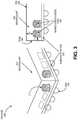
- FIG. 3 illustrates a package including one or more buried access ports and one or more means to access the buried access ports according to an embodiment.
- FIG. 3 provides an angle view and a side view of a package 300 , such as system in package, with ball grid array (BGA) 350 .
- BGA ball grid array
- embodiments are not limited to a particular type or structure of electronic package.
- the package 300 includes one or more buried access ports to provide electrical connections to the encapsulated system.
- the package 300 includes one or more electrically conductive access ports 310 on the substrate or PCB 320 .
- the one or more electrically conductive access ports 310 are buried within the encapsulant 330 of the package.
- the construction of the access ports may vary depending on the implementation, and may include, but are not limited to, solder paste, pre-formed solder spheres, a copper post, a small piece of PCB, or other similar element that allows for electrical contact when a physical contact is made with a probe.
- the buried access ports are fully enclosed in the encapsulant and insulated from electrical contact by the encapsulant material, and thus it is not possible to make electrical contact with the access ports without breaking through the encapsulant.
- the one or more access ports 310 are buried within the encapsulant near the top surface or edge of the encapsulated portion of the package (for example, adjacent to the package edge) such that testing may be accomplished by reaching the one or more access ports through the encapsulant, such as by drilling through, piercing through, or otherwise breaking through the encapsulant, to provide an electrical connection to the system at the appropriate debug access points of the system 300 .
- the one or more access ports 310 may alternatively be accessed utilizing electromagnetic coupling with one or more ports without breaking through the encapsulate.
- each access port 310 may be optimized per the appropriate design requirements.
- a buried access port may located so that the access port is a closest element of the package to an edge 340 of the package, to the top surface 345 of the package, or both to allow for ease of access to such buried access ports.
- the buried debug access ports 310 are fully encapsulated, thus protecting against accidental electrical contact, and providing that the package moisture integrity remains intact.
- FIG. 4 illustrates a package including one or more buried access ports and one or more means to access the buried access ports according to an embodiment.
- FIG. 4 provides a side view of the package 400 .
- the package 400 includes one or more buried access ports to provide electrical connections to the encapsulated system.
- the one or more buried access ports 410 are enclosed in the encapsulant of the package 400 , the access ports being located near to a top or side of the package.
- electrical contact may be made with the buried access ports for connection with a debug tool 450 .
- the access may be made by drilling through, piercing through, or otherwise breaking through the encapsulant to reach the buried access ports.
- access may be made through use of a connector or lead that is capable of breaking through the thin layer of encapsulant 430 .
- the access with the buried access port may be made by electromagnetic coupling with one or more ports, which be provided without breaking through the encapsulant.
- FIG. 5 is a flowchart to illustrate fabrication of a package with buried electrical debug access ports according to an embodiment.
- a fabrication process 500 may include, but is not limited to, the following:
- the access ports are generated and installed such that access ports are near to a top surface or side surface of the completed package.
- the process may include thinning of the encapsulant as required for the construction of the package. Any thinning process will not provide access the one or more buried access ports, which are to be fully encapsulated in the finished package.
- FIG. 6 is a flowchart to a debugging process for package with buried electrical debug access ports according to an embodiment.
- a debug process 600 may include, but is not limited to, the following:
- the testing sequence may in certain cases identify one or more error conditions in the package.
- Accessing the ports may include drilling through, piercing, or otherwise breaking through the encapsulant of the package to reach the debug access ports, or may include by electromagnetic coupling with one or more access ports.
- FIG. 7 is an illustration of components of an apparatus or system including a system in package according to an embodiment.
- an electronic device or system 700 includes a system in package 710 , wherein the system in package 710 may provide storage or other function for the electronic device or system 700 .
- FIG. 7 illustrates an example, and embodiments are not limited to a particular package technology, or to a particular electronic device or system.
- the electronic device or system 700 may include, but is not limited to, a mobile electronic device.
- the system in package (SiP) 710 may include one or more ASICs, or controllers, or other processing element 714 (generally referred to herein as an ASIC) coupled to one or more buses or interconnects, shown in general as bus 712 .
- the bus 712 is a communication means for transmission of data.
- the bus 712 is illustrated as a single bus for simplicity, but may represent multiple different interconnects (including an RDL (Redistribution Layer) and via) or buses and the component connections to such interconnects or buses may vary.
- the bus 712 shown in FIG. 7 is an abstraction that represents any one or more separate physical buses, point-to-point connections, or both connected by appropriate bridges, adapters, or controllers.
- the SiP 710 includes one more buried electrical access ports, illustrated as access ports 740 and 742 .
- the access ports 740 - 742 are fully encapsulated in the package, and do not allow electrical contact with the access ports without breaking through the encapsulant for the SiP 710 .
- the SiP 710 further comprises a memory 716 for storing information and instructions to be executed by the ASIC 714 .
- Memory 716 may include, but is not limited to, dynamic random access memory (DRAM).
- the SiP 710 also may comprise solid state memory (SSD) to provide storage, the SSD including non-volatile memory.
- the SiP 710 may further a read only memory (ROM) 720 or other static storage device for storing static information and instructions.
- ROM read only memory
- the SiP 710 may include one or more transmitters or receivers 730 coupled to the bus 712 for wireless or wired communication of data.
- the SiP 710 may include one or more ports 732 for the transmission and reception of data via wired communications and one or more antennae for the for the transmission and reception of data via wireless communication.
- Wireless communication includes, but is not limited to, Wi-Fi, BluetoothTM, near field communication, and other wireless communication standards.
- the SiP 710 may include one or more sensors 722 to sense environmental factors, wherein the one or more sensors may include a temperature sensor, a voltage sensor, or other sensor.
- the device or system 700 includes a motherboard 760 , wherein the SiP 710 is installed on the motherboard by soldering of a ball grid array or other known connection means.
- the access ports 740 - 742 may be utilized to provide debug access to the SiP while the SiP is installed on the motherboard 760
- the device or system 700 may include additional components, such as one or more processors 770 to process data, and a power source such as a battery 772 to power the system or apparatus 700 .
- the power source may further include a solar cell, a fuel cell, a charged capacitor, near field inductive coupling, or other system or device for providing or generating power.
- the power provided by the power source may be distributed as required to elements of the system or apparatus 700 .
- Various embodiments may include various processes. These processes may be performed by hardware components or may be embodied in computer program or machine-executable instructions, which may be used to cause a general-purpose or special-purpose processor or logic circuits programmed with the instructions to perform the processes. Alternatively, the processes may be performed by a combination of hardware and software.
- Portions of various embodiments may be provided as a computer program product, which may include a computer-readable medium having stored thereon computer program instructions, which may be used to program a computer (or other electronic devices) for execution by one or more processors to perform a process according to certain embodiments.
- the computer-readable medium may include, but is not limited to, magnetic disks, optical disks, read-only memory (ROM), random access memory (RAM), erasable programmable read-only memory (EPROM), electrically-erasable programmable read-only memory (EEPROM), magnetic or optical cards, flash memory, or other type of computer-readable medium suitable for storing electronic instructions.
- embodiments may also be downloaded as a computer program product, wherein the program may be transferred from a remote computer to a requesting computer.
- element A may be directly coupled to element B or be indirectly coupled through, for example, element C.
- a component, feature, structure, process, or characteristic A “causes” a component, feature, structure, process, or characteristic B, it means that “A” is at least a partial cause of “B” but that there may also be at least one other component, feature, structure, process, or characteristic that assists in causing “B.” If the specification indicates that a component, feature, structure, process, or characteristic “may”, “might”, or “could” be included, that particular component, feature, structure, process, or characteristic is not required to be included. If the specification or claim refers to “a” or “an” element, this does not mean there is only one of the described elements.
- An embodiment is an implementation or example.
- Reference in the specification to “an embodiment,” “one embodiment,” “some embodiments,” or “other embodiments” means that a particular feature, structure, or characteristic described in connection with the embodiments is included in at least some embodiments, but not necessarily all embodiments.
- the various appearances of “an embodiment,” “one embodiment,” or “some embodiments” are not necessarily all referring to the same embodiments. It should be appreciated that in the foregoing description of exemplary embodiments, various features are sometimes grouped together in a single embodiment, figure, or description thereof for the purpose of streamlining the disclosure and aiding in the understanding of one or more of the various novel aspects. This method of disclosure, however, is not to be interpreted as reflecting an intention that the claimed embodiments requires more features than are expressly recited in each claim. Rather, as the following claims reflect, novel aspects lie in less than all features of a single foregoing disclosed embodiment. Thus, the claims are hereby expressly incorporated into this description, with each claim standing on its own as a separate embodiment.
- an apparatus includes a substrate or printed circuit board; one or more electronic components coupled with the substrate or printed circuit board; one or more electrical access ports coupled with the substrate or printed circuit board, each electrical access port including electrically conductive material; and an encapsulant material, wherein the encapsulant material encapsulates the one or more access ports.
- the one or more access ports are electrically connected to one or more circuits of the apparatus to provide debugging access to the apparatus.
- each of the one or more access ports is insulated from electrical contact by the encapsulant material.
- the apparatus is a system in package (SiP).
- each of the one or more access ports is adjacent to an edge of the encapsulant material.
- a first access port is a closest element of the apparatus to an edge of the encapsulant material.
- a first access port is a closest element of the apparatus to a top surface of the encapsulant material.
- the one or more electrical access ports are accessible by breaking through the encapsulate material.
- breaking through the encapsulate material includes drilling through or piercing through the encapsulate material.
- the one or more electrical access ports are accessible by electromagnetic coupling with at least one access port.
- a method includes installing one or more electronic components on a substrate or printed circuit board; installing one or more electrical access ports on the substrate or printed circuit board; and encapsulating the one more electronic components and one or more electrical access ports in an encapsulant material.
- the one more electrical access ports are fully encapsulated to generate one or more buried access ports.
- encapsulating the one or more buried access ports is to insulate the one or more buried access ports from electrical contact.
- installing the one or more electrical access ports on the substrate or printed circuit board includes installing each of the one or more electrical access ports adjacent to an edge of the encapsulant material.
- installing the one or more electrical access ports on the substrate or printed circuit board includes installing a first electrical access port to be a closest element of the package to an edge of the encapsulant material.
- installing the one or more electrical access ports on the substrate or printed circuit board includes installing a first electrical access port to be a closest element of the package to a top surface of the encapsulant material.
- the one or more buried access ports are accessible by breaking through the encapsulate material.
- the one or more electrical access ports are accessible by electromagnetic coupling with at least one access port.
- the method further includes accessing one or more buried access ports by breaking through the encapsulate material.
- the method further includes accessing one or more electrical access ports by electromagnetic coupling at least one access port.
- a system includes a processor; an electronic package; and a motherboard, the electronic package being installed in the motherboard.
- the electronic package includes a substrate or printed circuit board, a plurality of electronic components including a solid state drive (SSD) coupled with the substrate or printed circuit board, one or more electrical access ports coupled with the substrate or printed circuit board, each electrical access port including electrically conductive material, and an encapsulant material, wherein the encapsulant material encapsulates the one or more access ports.
- the one or more access ports are electrically connected to one or more circuits of the electronic package to provide debugging access to the electronic package.
- each of the one or more access ports is insulated from electrical contact by the encapsulant material.
- each of the one or more access ports of the electronic package is adjacent to an edge of the encapsulant material.
- a first access port is a closest element of the electronic package to an edge of the encapsulant material, to a top surface of the encapsulant material, or both.
- the one or more electrical access ports are accessible by breaking through the encapsulate material.
- the one or more electrical access ports are accessible by electromagnetic coupling with at least one access port.
- access to the electrical access ports provides debug access to the electronic package without removing the electronic package from the motherboard.
Landscapes
- Engineering & Computer Science (AREA)
- Microelectronics & Electronic Packaging (AREA)
- Computer Hardware Design (AREA)
- General Engineering & Computer Science (AREA)
- Physics & Mathematics (AREA)
- General Physics & Mathematics (AREA)
- Manufacturing & Machinery (AREA)
- Printing Elements For Providing Electric Connections Between Printed Circuits (AREA)
Abstract
Description
Claims (17)
Priority Applications (3)
| Application Number | Priority Date | Filing Date | Title |
|---|---|---|---|
| US15/089,385 US11064612B2 (en) | 2016-04-01 | 2016-04-01 | Buried electrical debug access port |
| PCT/US2017/017238 WO2017172061A1 (en) | 2016-04-01 | 2017-02-09 | Buried electrical debug access port |
| US17/338,450 US11700696B2 (en) | 2016-04-01 | 2021-06-03 | Buried electrical debug access port |
Applications Claiming Priority (1)
| Application Number | Priority Date | Filing Date | Title |
|---|---|---|---|
| US15/089,385 US11064612B2 (en) | 2016-04-01 | 2016-04-01 | Buried electrical debug access port |
Related Child Applications (1)
| Application Number | Title | Priority Date | Filing Date |
|---|---|---|---|
| US17/338,450 Division US11700696B2 (en) | 2016-04-01 | 2021-06-03 | Buried electrical debug access port |
Publications (2)
| Publication Number | Publication Date |
|---|---|
| US20170285097A1 US20170285097A1 (en) | 2017-10-05 |
| US11064612B2 true US11064612B2 (en) | 2021-07-13 |
Family
ID=59958660
Family Applications (2)
| Application Number | Title | Priority Date | Filing Date |
|---|---|---|---|
| US15/089,385 Active 2039-07-09 US11064612B2 (en) | 2016-04-01 | 2016-04-01 | Buried electrical debug access port |
| US17/338,450 Active 2036-04-14 US11700696B2 (en) | 2016-04-01 | 2021-06-03 | Buried electrical debug access port |
Family Applications After (1)
| Application Number | Title | Priority Date | Filing Date |
|---|---|---|---|
| US17/338,450 Active 2036-04-14 US11700696B2 (en) | 2016-04-01 | 2021-06-03 | Buried electrical debug access port |
Country Status (2)
| Country | Link |
|---|---|
| US (2) | US11064612B2 (en) |
| WO (1) | WO2017172061A1 (en) |
Families Citing this family (1)
| Publication number | Priority date | Publication date | Assignee | Title |
|---|---|---|---|---|
| US11355403B2 (en) | 2018-06-28 | 2022-06-07 | Western Digital Technologies, Inc. | Semiconductor device including through-package debug features |
Citations (7)
| Publication number | Priority date | Publication date | Assignee | Title |
|---|---|---|---|---|
| US7230309B2 (en) * | 2003-10-02 | 2007-06-12 | Infineon Technologies Ag | Semiconductor component and sensor component for data transmission devices |
| KR20080000879A (en) | 2006-06-28 | 2008-01-03 | 삼성전자주식회사 | Vijay semiconductor chip package and inspection method thereof |
| US7511299B1 (en) * | 2007-10-02 | 2009-03-31 | Xilinx, Inc. | Packaged integrated circuit with raised test points |
| US20130330846A1 (en) | 2012-06-12 | 2013-12-12 | Jinbang Tang | Test vehicles for encapsulated semiconductor device packages |
| US20140002998A1 (en) | 2012-06-28 | 2014-01-02 | Intel Corporation | High heat capacity electronic components and methods for fabricating |
| US20150228550A1 (en) | 2014-02-13 | 2015-08-13 | Taiwan Semiconductor Manufacturing Company, Ltd. | Integrated Circuit Package and Methods of Forming Same |
| US9978688B2 (en) * | 2013-02-28 | 2018-05-22 | Advanced Semiconductor Engineering, Inc. | Semiconductor package having a waveguide antenna and manufacturing method thereof |
-
2016
- 2016-04-01 US US15/089,385 patent/US11064612B2/en active Active
-
2017
- 2017-02-09 WO PCT/US2017/017238 patent/WO2017172061A1/en not_active Ceased
-
2021
- 2021-06-03 US US17/338,450 patent/US11700696B2/en active Active
Patent Citations (7)
| Publication number | Priority date | Publication date | Assignee | Title |
|---|---|---|---|---|
| US7230309B2 (en) * | 2003-10-02 | 2007-06-12 | Infineon Technologies Ag | Semiconductor component and sensor component for data transmission devices |
| KR20080000879A (en) | 2006-06-28 | 2008-01-03 | 삼성전자주식회사 | Vijay semiconductor chip package and inspection method thereof |
| US7511299B1 (en) * | 2007-10-02 | 2009-03-31 | Xilinx, Inc. | Packaged integrated circuit with raised test points |
| US20130330846A1 (en) | 2012-06-12 | 2013-12-12 | Jinbang Tang | Test vehicles for encapsulated semiconductor device packages |
| US20140002998A1 (en) | 2012-06-28 | 2014-01-02 | Intel Corporation | High heat capacity electronic components and methods for fabricating |
| US9978688B2 (en) * | 2013-02-28 | 2018-05-22 | Advanced Semiconductor Engineering, Inc. | Semiconductor package having a waveguide antenna and manufacturing method thereof |
| US20150228550A1 (en) | 2014-02-13 | 2015-08-13 | Taiwan Semiconductor Manufacturing Company, Ltd. | Integrated Circuit Package and Methods of Forming Same |
Non-Patent Citations (2)
| Title |
|---|
| International Preliminary Report on Patentability for International Patent Application No. PCT/US2017/017238 dated Oct. 11, 2018, 10 pages. |
| International Search Report and Written Opinion for International Patent Application No. PCT/US2017/017238 dated May 19, 2017, 13 pages. |
Also Published As
| Publication number | Publication date |
|---|---|
| US20170285097A1 (en) | 2017-10-05 |
| WO2017172061A1 (en) | 2017-10-05 |
| US20210298183A1 (en) | 2021-09-23 |
| US11700696B2 (en) | 2023-07-11 |
Similar Documents
| Publication | Publication Date | Title |
|---|---|---|
| US9589905B2 (en) | EMI shielding in semiconductor packages | |
| US10025354B2 (en) | System module and mobile computing device including the same | |
| US9024426B2 (en) | Semiconductor device and method of manufacturing the same | |
| CN205080908U (en) | Semiconductor device | |
| CN205621714U (en) | Semiconductor package | |
| KR101697603B1 (en) | Semiconductor Package | |
| US11557523B2 (en) | Semiconductor packages and methods of forming the semiconductor packages | |
| US10393799B2 (en) | Electronic device package | |
| US20140151863A1 (en) | Semiconductor packages and methods of fabricating the same | |
| US20110075387A1 (en) | Strain Measurement Chips For Printed Circuit Boards | |
| CN101499451B (en) | Printed circuit board, semiconductor package, card apparatus, and system | |
| US20170047310A1 (en) | Semiconductor package and method of manufacturing the same | |
| US8422236B2 (en) | Pin module and chip on board type use device | |
| US20120068350A1 (en) | Semiconductor packages, electronic devices and electronic systems employing the same | |
| US11700696B2 (en) | Buried electrical debug access port | |
| US20080156884A1 (en) | Memory card having double contact pads and method for manufacturing the same | |
| US9209133B2 (en) | Semiconductor apparatus | |
| US9041181B2 (en) | Land grid array package capable of decreasing a height difference between a land and a solder resist | |
| US8741665B2 (en) | Method of manufacturing semiconductor module | |
| CN215953778U (en) | Test equipment for signal extraction | |
| US12621970B2 (en) | Electromagnetic interference shield extending underneath memory modules | |
| CN110866518B (en) | Narrow encapsulation fingerprint module and fingerprint identification mobile terminal | |
| US20240112966A1 (en) | Multisided integrated circuit assembly | |
| US20250311180A1 (en) | Electromagnetic interference shield extending underneath memory modules | |
| CN117835522A (en) | Encrypted circuit board, encrypted packaging board and packaging module detection method |
Legal Events
| Date | Code | Title | Description |
|---|---|---|---|
| AS | Assignment |
Owner name: INTEL CORPORATION, CALIFORNIA Free format text: ASSIGNMENT OF ASSIGNORS INTEREST;ASSIGNORS:PON, FLORENCE R.;KHALAF, BILAL;SHOJAIE, SAEED S.;REEL/FRAME:038232/0670 Effective date: 20160407 |
|
| STCT | Information on status: administrative procedure adjustment |
Free format text: PROSECUTION SUSPENDED |
|
| STPP | Information on status: patent application and granting procedure in general |
Free format text: DOCKETED NEW CASE - READY FOR EXAMINATION |
|
| STPP | Information on status: patent application and granting procedure in general |
Free format text: NON FINAL ACTION MAILED |
|
| STPP | Information on status: patent application and granting procedure in general |
Free format text: RESPONSE TO NON-FINAL OFFICE ACTION ENTERED AND FORWARDED TO EXAMINER |
|
| STPP | Information on status: patent application and granting procedure in general |
Free format text: FINAL REJECTION MAILED |
|
| STPP | Information on status: patent application and granting procedure in general |
Free format text: RESPONSE AFTER FINAL ACTION FORWARDED TO EXAMINER |
|
| STPP | Information on status: patent application and granting procedure in general |
Free format text: DOCKETED NEW CASE - READY FOR EXAMINATION |
|
| STPP | Information on status: patent application and granting procedure in general |
Free format text: NOTICE OF ALLOWANCE MAILED -- APPLICATION RECEIVED IN OFFICE OF PUBLICATIONS |
|
| STPP | Information on status: patent application and granting procedure in general |
Free format text: PUBLICATIONS -- ISSUE FEE PAYMENT RECEIVED |
|
| STPP | Information on status: patent application and granting procedure in general |
Free format text: PUBLICATIONS -- ISSUE FEE PAYMENT VERIFIED |
|
| STCF | Information on status: patent grant |
Free format text: PATENTED CASE |
|
| MAFP | Maintenance fee payment |
Free format text: PAYMENT OF MAINTENANCE FEE, 4TH YEAR, LARGE ENTITY (ORIGINAL EVENT CODE: M1551); ENTITY STATUS OF PATENT OWNER: LARGE ENTITY Year of fee payment: 4 |