US11056525B2 - Semiconductor photomultiplier - Google Patents
Semiconductor photomultiplier Download PDFInfo
- Publication number
- US11056525B2 US11056525B2 US15/335,658 US201615335658A US11056525B2 US 11056525 B2 US11056525 B2 US 11056525B2 US 201615335658 A US201615335658 A US 201615335658A US 11056525 B2 US11056525 B2 US 11056525B2
- Authority
- US
- United States
- Prior art keywords
- microcells
- semiconductor
- photomultiplier
- semiconductor substrate
- bus line
- Prior art date
- Legal status (The legal status is an assumption and is not a legal conclusion. Google has not performed a legal analysis and makes no representation as to the accuracy of the status listed.)
- Active, expires
Links
Images


Classifications
-
- H—ELECTRICITY
- H10—SEMICONDUCTOR DEVICES; ELECTRIC SOLID-STATE DEVICES NOT OTHERWISE PROVIDED FOR
- H10F—INORGANIC SEMICONDUCTOR DEVICES SENSITIVE TO INFRARED RADIATION, LIGHT, ELECTROMAGNETIC RADIATION OF SHORTER WAVELENGTH OR CORPUSCULAR RADIATION
- H10F39/00—Integrated devices, or assemblies of multiple devices, comprising at least one element covered by group H10F30/00, e.g. radiation detectors comprising photodiode arrays
- H10F39/10—Integrated devices
- H10F39/12—Image sensors
- H10F39/18—Complementary metal-oxide-semiconductor [CMOS] image sensors; Photodiode array image sensors
-
- H01L27/14643—
-
- H01L23/481—
-
- H01L27/1443—
-
- H01L27/1446—
-
- H01L27/14603—
-
- H01L27/14609—
-
- H01L27/14634—
-
- H01L27/14636—
-
- H01L28/20—
-
- H01L31/107—
-
- H—ELECTRICITY
- H10—SEMICONDUCTOR DEVICES; ELECTRIC SOLID-STATE DEVICES NOT OTHERWISE PROVIDED FOR
- H10D—INORGANIC ELECTRIC SEMICONDUCTOR DEVICES
- H10D1/00—Resistors, capacitors or inductors
- H10D1/40—Resistors
- H10D1/47—Resistors having no potential barriers
-
- H—ELECTRICITY
- H10—SEMICONDUCTOR DEVICES; ELECTRIC SOLID-STATE DEVICES NOT OTHERWISE PROVIDED FOR
- H10F—INORGANIC SEMICONDUCTOR DEVICES SENSITIVE TO INFRARED RADIATION, LIGHT, ELECTROMAGNETIC RADIATION OF SHORTER WAVELENGTH OR CORPUSCULAR RADIATION
- H10F30/00—Individual radiation-sensitive semiconductor devices in which radiation controls the flow of current through the devices, e.g. photodetectors
- H10F30/20—Individual radiation-sensitive semiconductor devices in which radiation controls the flow of current through the devices, e.g. photodetectors the devices having potential barriers, e.g. phototransistors
- H10F30/21—Individual radiation-sensitive semiconductor devices in which radiation controls the flow of current through the devices, e.g. photodetectors the devices having potential barriers, e.g. phototransistors the devices being sensitive to infrared, visible or ultraviolet radiation
- H10F30/22—Individual radiation-sensitive semiconductor devices in which radiation controls the flow of current through the devices, e.g. photodetectors the devices having potential barriers, e.g. phototransistors the devices being sensitive to infrared, visible or ultraviolet radiation the devices having only one potential barrier, e.g. photodiodes
- H10F30/225—Individual radiation-sensitive semiconductor devices in which radiation controls the flow of current through the devices, e.g. photodetectors the devices having potential barriers, e.g. phototransistors the devices being sensitive to infrared, visible or ultraviolet radiation the devices having only one potential barrier, e.g. photodiodes the potential barrier working in avalanche mode, e.g. avalanche photodiodes
-
- H—ELECTRICITY
- H10—SEMICONDUCTOR DEVICES; ELECTRIC SOLID-STATE DEVICES NOT OTHERWISE PROVIDED FOR
- H10F—INORGANIC SEMICONDUCTOR DEVICES SENSITIVE TO INFRARED RADIATION, LIGHT, ELECTROMAGNETIC RADIATION OF SHORTER WAVELENGTH OR CORPUSCULAR RADIATION
- H10F39/00—Integrated devices, or assemblies of multiple devices, comprising at least one element covered by group H10F30/00, e.g. radiation detectors comprising photodiode arrays
- H10F39/10—Integrated devices
- H10F39/103—Integrated devices the at least one element covered by H10F30/00 having potential barriers, e.g. integrated devices comprising photodiodes or phototransistors
-
- H—ELECTRICITY
- H10—SEMICONDUCTOR DEVICES; ELECTRIC SOLID-STATE DEVICES NOT OTHERWISE PROVIDED FOR
- H10F—INORGANIC SEMICONDUCTOR DEVICES SENSITIVE TO INFRARED RADIATION, LIGHT, ELECTROMAGNETIC RADIATION OF SHORTER WAVELENGTH OR CORPUSCULAR RADIATION
- H10F39/00—Integrated devices, or assemblies of multiple devices, comprising at least one element covered by group H10F30/00, e.g. radiation detectors comprising photodiode arrays
- H10F39/10—Integrated devices
- H10F39/107—Integrated devices having multiple elements covered by H10F30/00 in a repetitive configuration, e.g. radiation detectors comprising photodiode arrays
-
- H—ELECTRICITY
- H10—SEMICONDUCTOR DEVICES; ELECTRIC SOLID-STATE DEVICES NOT OTHERWISE PROVIDED FOR
- H10F—INORGANIC SEMICONDUCTOR DEVICES SENSITIVE TO INFRARED RADIATION, LIGHT, ELECTROMAGNETIC RADIATION OF SHORTER WAVELENGTH OR CORPUSCULAR RADIATION
- H10F39/00—Integrated devices, or assemblies of multiple devices, comprising at least one element covered by group H10F30/00, e.g. radiation detectors comprising photodiode arrays
- H10F39/80—Constructional details of image sensors
- H10F39/802—Geometry or disposition of elements in pixels, e.g. address-lines or gate electrodes
-
- H—ELECTRICITY
- H10—SEMICONDUCTOR DEVICES; ELECTRIC SOLID-STATE DEVICES NOT OTHERWISE PROVIDED FOR
- H10F—INORGANIC SEMICONDUCTOR DEVICES SENSITIVE TO INFRARED RADIATION, LIGHT, ELECTROMAGNETIC RADIATION OF SHORTER WAVELENGTH OR CORPUSCULAR RADIATION
- H10F39/00—Integrated devices, or assemblies of multiple devices, comprising at least one element covered by group H10F30/00, e.g. radiation detectors comprising photodiode arrays
- H10F39/80—Constructional details of image sensors
- H10F39/803—Pixels having integrated switching, control, storage or amplification elements
-
- H—ELECTRICITY
- H10—SEMICONDUCTOR DEVICES; ELECTRIC SOLID-STATE DEVICES NOT OTHERWISE PROVIDED FOR
- H10F—INORGANIC SEMICONDUCTOR DEVICES SENSITIVE TO INFRARED RADIATION, LIGHT, ELECTROMAGNETIC RADIATION OF SHORTER WAVELENGTH OR CORPUSCULAR RADIATION
- H10F39/00—Integrated devices, or assemblies of multiple devices, comprising at least one element covered by group H10F30/00, e.g. radiation detectors comprising photodiode arrays
- H10F39/80—Constructional details of image sensors
- H10F39/809—Constructional details of image sensors of hybrid image sensors
-
- H—ELECTRICITY
- H10—SEMICONDUCTOR DEVICES; ELECTRIC SOLID-STATE DEVICES NOT OTHERWISE PROVIDED FOR
- H10F—INORGANIC SEMICONDUCTOR DEVICES SENSITIVE TO INFRARED RADIATION, LIGHT, ELECTROMAGNETIC RADIATION OF SHORTER WAVELENGTH OR CORPUSCULAR RADIATION
- H10F39/00—Integrated devices, or assemblies of multiple devices, comprising at least one element covered by group H10F30/00, e.g. radiation detectors comprising photodiode arrays
- H10F39/80—Constructional details of image sensors
- H10F39/811—Interconnections
-
- H—ELECTRICITY
- H10—SEMICONDUCTOR DEVICES; ELECTRIC SOLID-STATE DEVICES NOT OTHERWISE PROVIDED FOR
- H10W—GENERIC PACKAGES, INTERCONNECTIONS, CONNECTORS OR OTHER CONSTRUCTIONAL DETAILS OF DEVICES COVERED BY CLASS H10
- H10W20/00—Interconnections in chips, wafers or substrates
- H10W20/20—Interconnections within wafers or substrates, e.g. through-silicon vias [TSV]
-
- G—PHYSICS
- G01—MEASURING; TESTING
- G01J—MEASUREMENT OF INTENSITY, VELOCITY, SPECTRAL CONTENT, POLARISATION, PHASE OR PULSE CHARACTERISTICS OF INFRARED, VISIBLE OR ULTRAVIOLET LIGHT; COLORIMETRY; RADIATION PYROMETRY
- G01J1/00—Photometry, e.g. photographic exposure meter
- G01J1/42—Photometry, e.g. photographic exposure meter using electric radiation detectors
- G01J1/44—Electric circuits
- G01J2001/4446—Type of detector
- G01J2001/446—Photodiode
- G01J2001/4466—Avalanche
Definitions
- the present disclosure relates to photon detectors.
- the present disclosure relates to high sensitivity photon detectors such as semiconductor photomultipliers.
- the present disclosure relates to semiconductor photomultipliers (SiPMs or SPMs) in such areas as Positron Emission Tomography [PET], including Time-Of-Flight PET [TOF-PET], Laser Ranging [LIDAR] applications, bio luminescence, High Energy Physics [HEP] detectors.
- PET Positron Emission Tomography
- TOF-PET Time-Of-Flight PET
- LIDAR Laser Ranging
- HEP High Energy Physics
- SiPMs are semiconductor photon sensitive devices made up of an array of very small Geiger-mode avalanche photodiode (APD) cells on a substrate such as silicon.
- APD cells vary in dimension from several micron to 100 microns depending on the mask used, and can have a typical density of up to 3000 microcells/sq. mm.
- Avalanche diodes can also be made from other semiconductors besides silicon, depending on the properties that are desirable.
- Silicon detects in the visible and near infrared range, with low multiplication noise (excess noise).
- Germanium (Ge) detects infrared to 1.7 ⁇ m wavelength, but has high multiplication noise.
- InGaAs Indium Gallium Arsenide detects to a maximum wavelength of 1.6 ⁇ m, and has less multiplication noise than Ge. InGaAs is generally used for the multiplication region of a heterostructure diode, is compatible with high speed telecommunications using optical fibres, and can reach speeds of greater than Gbit/s.
- Gallium nitride operates with UV light.
- HgCdTe Mercury Cadmium Telluride
- operates in the infrared to a maximum wavelength of about 14 ⁇ m, requires cooling to reduce dark currents, and can achieve a very low level of excess noise.
- Silicon avalanche diodes can function with breakdown voltages of 100 to >1000V, typically.
- APDs exhibit internal current gain effect of about 100-1000 due to impact ionization, or avalanche effect, when a high reverse bias voltage is applied (approximately 100->200 V in silicon, depending on the doping profile in the junction).
- Silicon Photomultipliers or SiPMs can achieve a gain of 10 5 to 10 6 by using Geiger mode APDs also known as Single Photon Avalanche Diodes (SPADs) which operate with a reverse voltage that is greater than the breakdown voltage, and by maintaining the dark count event rate at a sufficiently low level.
- the current generated by an avalanche event must be quenched by an appropriate current limited scheme so that the device can recover and reset after an avalanche event.
- SiPM sensors have lower operating voltages than APDs and have a breakdown voltage from 10-100 Volts.
- Silicon Photomultipliers typically include a matrix of major and minor bus lines.
- the minor bus lines connect directly to the microcells.
- the minor bus lines are then joined to bond pads by a major bus line.
- the minor bus lines are loaded with the inductance, capacitance and resistance of the microcells.
- the major bus lines are then loaded with the inductance, capacitance and resistance of the minor bus lines.
- the rise time, delay and recovery time of signal from a microcell on the SiPM will therefore depend strongly on its position in the SiPM.
- the variation in rise time and delay across the array will give rise to increased jitter and therefore increased coincidence resolving time (CRT) or timing jitter.
- CRT coincidence resolving time
- a semiconductor photomultiplier comprising:
- the photosensitive element comprises a single photon avalanche diode (SPAD).
- SPAD single photon avalanche diode
- a quench element is associated with each SPAD.
- the quench element is a passive component resistor.
- the quench element is an active component transistor.
- each segment of the segmented secondary bus line has an associated via coupled to a corresponding primary bus line.
- each photosensitive element is part of a microcell.
- At least some of the segments of the segmented secondary bus line are of equal length in order to equalise the signal delays from the microcells to the one or more terminals.
- the length of at least some of the primary bus lines are of equal length in order to equalise the signal delays from the microcells to the one or more terminals.
- each microcell comprises a photodiode.
- each microcell comprises a resistor coupled in series to the photodiode.
- a capacitive element is provided.
- the interconnected photosensitive elements are arranged in a grid configuration.
- the primary buses lines are parallel to columns in the grid configuration.
- at least some of the primary bus lines extend between the columns.
- each photosensitive element comprises an avalanche photodiode or a single photon avalanche diode.
- each interconnected photosensitive element comprises a quench resistor coupled in series to the avalanche photodiode or a single photon avalanche diode.
- the present disclosure relates to a substrate comprising:
- the present disclosure also relates to a method of fabricating a semiconductor photomultiplier; the method comprising:
- FIG. 1 illustrates an exemplary structure of a silicon photomultiplier.
- FIG. 2 is a schematic circuit diagram of an exemplary silicon photomultiplier.
- FIG. 3 is a schematic circuit diagram of an exemplary silicon photomultiplier.
- FIG. 4 is a top plan view of an exemplary silicon photomultiplier.
- FIG. 5 is a diagrammatic view of four microcells.
- FIG. 6 is a graph showing that signal delay, rise time and overall shape depend on the position of the microcell.
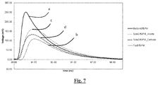
- FIG. 7 is a graph showing that signal delay, rise time and overall shape depend on the position of the microcell.
- FIG. 8 is a graph which shows the signal from the microcells furthest from the major row (furthest from terminal) compared with the signal from those closest to it.
- FIG. 9 shows a cross sectional view of a photomultiplier in accordance with the present teaching.
- FIG. 10 is a plan view of a bottom surface of the photomultiplier of FIG. 9 .
- FIG. 11 is a simulated graph of the signals on a segmented bus line on the bottom surface of the photomultiplier of FIG. 9 .
- FIG. 12 is a diagrammatic illustration of primary and secondary bus lines of the photomultiplier in accordance with the present teaching.
- FIG. 13 is a plan view of a bottom surface of the photomultiplier in accordance with the present teaching.
- FIG. 14 is a diagrammatic illustration of primary and secondary bus lines of the photomultiplier in accordance with the present teaching.
- a silicon photomultiplier 100 comprising an array of Geiger mode photodiodes is shown.
- the array is formed on a semiconductor substrate 150 using semiconductor processes which will be known to one skilled in the art and may include for example, but not limited to, deposition, implantation, diffusion, patterning, doping, and etching. Patterned layers of conducting material, insulating material and doped areas of semiconductor form the structure of the photodiode.
- a quench resistor is provided adjacent to each photodiode which may be used to limit the avalanche current.
- the photodiodes are electrically connected to common biasing and ground electrodes by aluminium or similar conductive tracking.
- the Silicon Photomultiplier 100 integrates a dense array of small, electrically and optically isolated Geigermode photodiodes 115 . Each photodiode 115 is coupled in series to a quench resistor 120 . Each photodiode 115 and its associated quench resistor 120 are referred to as a microcell 125 . The number of microcells 125 typically number between 100 and 3000 per mm 2 . The signals of all microcells 125 are then summed to form the output of the SiPM 100 . A simplified electrical circuit 130 is provided to illustrate the concept in FIG. 2 . Each microcell 125 detects photons identically and independently. The sum of the discharge currents from each of these individual binary detectors combines to form a quasi-analog output, and is thus capable of giving information on the magnitude of an incident photon flux.
- Each microcell 125 generates a highly uniform and quantized amount of charge every time the microcell 125 undergoes a Geiger breakdown.
- the gain of a microcell 125 (and hence the detector) is defined as the ratio of the output charge to the charge on an electron.
- the output charge can be calculated from the over-voltage and the microcell capacitance.
- FIG. 3 illustrates a silicon photomultiplier 300 described in PCT Patent Application no. WO 2011/117309 of which the present assignee is the applicant, the contents are incorporated herein by reference.
- the SPM 300 has a third electrode 305 which is capacitively coupled to each photodiode cathode 310 in order to provide a fast readout of the avalanche signals from the photodiodes 315 .
- the photodiode 315 emits a current pulse, part of the resulting change in voltage at the cathode 310 will be coupled via mutual capacitance 320 into the third (fast) electrode 305 .
- Using the third electrode 305 for readout avoids the compromised transient performance resulting from the relatively large RC time constant associated with the biasing circuit.
- silicon photomultipliers comprise major bus lines 440 and minor bus lines 450 as illustrated in FIG. 4 .
- the minor bus lines 450 connect directly to the microcells 125 .
- the minor bus lines 450 are then coupled to major bus line 440 which connect to the bond pads associated with the terminals 370 and 305 .
- the minor bus lines 450 extend vertically between the columns of microcells 125 ; while the major bus lines 440 extend horizontally adjacent the outer row of the microcells 125 .
- the minor bus lines 450 are loaded with the inductance, capacitance and resistance of the microcells 125 .
- the major bus lines 440 are then loaded with the inductance, capacitance and resistance of the minor bus lines 450 .
- the rise time, delay and recovery time of signal from a microcell 125 on the SiPM will therefore depend significantly on its position in the SiPM.
- the variation in rise time and delay across the array will give rise to increased jitter and therefore increased coincidence resolving time (CRT).
- CRT coincidence resolving time
- FIGS. 5 and 6 which shows experimental data to quantify the range of delays and rise times seen across a SiPM. Pulses coming from different areas of the SiPM were compared by partially (85%) blacking out areas as indicated by labels a, b, c, and d in FIG. 5 .
- FIGS. 6 and 7 illustrate the standard terminal 370 and fast output terminal 305 signal delay, rise time and overall shape depend strongly on position on the major row.
- FIG. 6 illustrates the signals measured at the standard terminal 370
- FIG. 7 illustrates the signals measured at the fast terminal 305 .
- the delay from difference between ‘a’ and ‘b’ is approximately 400 ps.
- the graph of FIG. 8 shows the signal from fourteen microcells furthest from the major row (anode terminal) compared with the signal from fourteen microcells closest to major row (anode terminal). It is clear that there is significant time delay between the two signals. It is desirable to segment the major bus line in order to reduce the load on the signal. If the segments were joined together on top of the substrate 150 , the area taken up by the additional bus lines would be subtracted from the optically active area, significantly reducing the photo-detection efficiency (PDE).
- PDE photo-detection efficiency
- the minor bus lines 950 extend vertically between the columns of microcells 125 similar as previously described with reference to FIG. 4 .
- the major bus lines 940 are provided on a lower surface 960 of the substrate 150 and are operably coupled to the minor bus lines 950 via true silicon vias (TSVs) 970 .
- TSVs true silicon vias
- the minor bus lines 950 interconnect the microcells 125 which are formed on an upper surface 965 of the substrate 150 .
- the TSVs 970 are vertical connections which pass completely through the substrate 150 .
- the number of major bus lines 940 which may be used is significantly increased compared to the arrangement of FIG.
- the major bus line 940 is segmented into multiple segments 980 as illustrated in FIG. 10 . In the exemplary, six segments 980 extend horizontally on the bottom surface 960 of the substrate 150 . It is will be appreciated by those skilled in the art that the major bus line 940 may be segmented into any desirable number of segments 980 . Routing the major bus lines 940 under the silicon substrate 150 minimises the impact on the optically active area of the SiPM. It will be clear to those skilled in the art that CRT is strongly dependent on the range of delay seen across the array of microcells in the SiPM. Reducing the range of delay by segmenting the major bus lines 940 will reduce CRT.
- FIG. 11 is a simulated graph of the SiPM of FIG. 10 showing the signal delay, rise time and overall shape of the signal of four different segments connected to different major bus lengths ( 980 ).
- the signal delay between the fastest and slowest signal is approximately 150 ps.
- making the major bus lengths equal under the silicon will reduce the delay range further, thereby reducing CRT.
- Such a scheme is illustrated in FIG. 13 .
- FIG. 12 shows TSVs positioned along the major row associated with the standard terminal 370 and TSVs positioned along the major row associated with the fast terminal 305 .
- TSVs allows the arrays of micro cells 125 on top surface 965 of the substrate 150 to be segmented so that the major rows are shorted.
- the major and minor rows may be connected to the under side of the substrate at various positions in the area of the die and shorted via copper tracks. This will effectively reduce the load on each segment of microcells 125 .
- the reduced load will lead to a reduced range of delays (jitter and CRT). Further reductions in jitter can be achieved by using minor rows of various lengths so that the minor row load seen by a microcell furthest from the terminal is smallest and that seen by a microcell closest to the terminal is largest.
- FIG. 13 there illustrated a segmented major bus line on the bottom surface 960 of the substrate 150 .
- the major bus line is similar to the arrangement described in FIG. 10 with the exception that track length is increased in order to equalise the signal delays from the microcells 125 to the terminals. This is possible because due to the extra space under the substrate 150 to route the metal lines.
- FIG. 14 there is illustrated an exemplary arrangement of the minor bus lines where the signal paths from the microcells to the terminals are equalised.
- the signal path from position A to the terminal is approximately equal to signal path from position B.
- Such a scheme can be incorporated with the arrangement illustrated in FIGS. 9, 10, 12, 13 in order to further reduce the delay range.
- the silicon photomultiplier of the present teaching may be fabricated on the substrate 150 using conventional semiconductor processing techniques and may include for example, but not limited to, deposition, implantation, diffusion, patterning, doping, and etching. Patterned layers of conducting material, insulating material and doped areas of semiconductor form the structure of the microcells.
- semiconductor photomultiplier is intended to cover any solid state photomultiplier device such as Silicon Photomultiplier [SiPM], MicroPixel Photon Counters [MPPC], MicroPixel Avalanche Photodiodes [MAPD] but not limited to.
Landscapes
- Light Receiving Elements (AREA)
- Measurement Of Radiation (AREA)
Abstract
Description
-
- a substrate;
- an array of photosensitive elements formed on a first major surface of the substrate;
- a plurality of primary bus lines interconnecting the photosensitive elements;
- at least one segmented secondary bus line provided on a second major surface of the substrate which is operably coupled to one or more terminals; and
- multiple vertical interconnect access (vias) extending through the substrate operably coupling the primary bus lines to the at least one segmented secondary bus line.
-
- forming an array of photosensitive elements on a first major surface of a substrate;
- providing a plurality of primary bus lines interconnecting the photosensitive elements;
- providing at least one segmented secondary bus line on a second major surface of the substrate which is operably coupled to one or more terminals; and
- providing multiple vertical interconnect access (vias) extending through the substrate operably coupling the primary bus lines to the at least one segmented secondary bus line.
Where:
-
- G is the gain of the microcell;
- C is the capacitance of the microcell;
- ΔV is the over-voltage; and
- q is the charge of an electron.
-
- a) The minor rows closest to the anode were exposed. The signal path along the major row is short.
- b) The minor rows at the end of the major rows were exposed. This is the opposite of (a). The signal path along the major row will be long.
- c) The microcells on the minor bus closest to the major bus are exposed. The signal path along the minor rows will be short.
- d) The micro cells on the minor bus furthest from the major row are exposed. The signal path along the minor rows will be long.
Claims (17)
Priority Applications (1)
| Application Number | Priority Date | Filing Date | Title |
|---|---|---|---|
| US15/335,658 US11056525B2 (en) | 2014-12-19 | 2016-10-27 | Semiconductor photomultiplier |
Applications Claiming Priority (2)
| Application Number | Priority Date | Filing Date | Title |
|---|---|---|---|
| US14/577,123 US20160181302A1 (en) | 2014-12-19 | 2014-12-19 | Semiconductor photomultiplier |
| US15/335,658 US11056525B2 (en) | 2014-12-19 | 2016-10-27 | Semiconductor photomultiplier |
Related Parent Applications (1)
| Application Number | Title | Priority Date | Filing Date |
|---|---|---|---|
| US14/577,123 Division US20160181302A1 (en) | 2014-12-19 | 2014-12-19 | Semiconductor photomultiplier |
Publications (2)
| Publication Number | Publication Date |
|---|---|
| US20170047372A1 US20170047372A1 (en) | 2017-02-16 |
| US11056525B2 true US11056525B2 (en) | 2021-07-06 |
Family
ID=56130373
Family Applications (2)
| Application Number | Title | Priority Date | Filing Date |
|---|---|---|---|
| US14/577,123 Abandoned US20160181302A1 (en) | 2014-12-19 | 2014-12-19 | Semiconductor photomultiplier |
| US15/335,658 Active 2035-12-03 US11056525B2 (en) | 2014-12-19 | 2016-10-27 | Semiconductor photomultiplier |
Family Applications Before (1)
| Application Number | Title | Priority Date | Filing Date |
|---|---|---|---|
| US14/577,123 Abandoned US20160181302A1 (en) | 2014-12-19 | 2014-12-19 | Semiconductor photomultiplier |
Country Status (1)
| Country | Link |
|---|---|
| US (2) | US20160181302A1 (en) |
Families Citing this family (33)
| Publication number | Priority date | Publication date | Assignee | Title |
|---|---|---|---|---|
| US20160181302A1 (en) | 2014-12-19 | 2016-06-23 | Sensl Technologies Ltd | Semiconductor photomultiplier |
| JP6932580B2 (en) | 2017-08-04 | 2021-09-08 | ソニーセミコンダクタソリューションズ株式会社 | Solid-state image sensor |
| US10340408B1 (en) | 2018-05-17 | 2019-07-02 | Hi Llc | Non-invasive wearable brain interface systems including a headgear and a plurality of self-contained photodetector units configured to removably attach to the headgear |
| US10515993B2 (en) | 2018-05-17 | 2019-12-24 | Hi Llc | Stacked photodetector assemblies |
| US10158038B1 (en) | 2018-05-17 | 2018-12-18 | Hi Llc | Fast-gated photodetector architectures comprising dual voltage sources with a switch configuration |
| US10420498B1 (en) | 2018-06-20 | 2019-09-24 | Hi Llc | Spatial and temporal-based diffusive correlation spectroscopy systems and methods |
| US11213206B2 (en) | 2018-07-17 | 2022-01-04 | Hi Llc | Non-invasive measurement systems with single-photon counting camera |
| WO2020131148A1 (en) | 2018-12-21 | 2020-06-25 | Hi Llc | Biofeedback for awareness and modulation of mental state using a non-invasive brain interface system and method |
| WO2020226840A1 (en) | 2019-05-06 | 2020-11-12 | Hi Llc | Photodetector architectures for time-correlated single photon counting |
| WO2020236371A1 (en) | 2019-05-21 | 2020-11-26 | Hi Llc | Photodetector architectures for efficient fast-gating |
| US10868207B1 (en) | 2019-06-06 | 2020-12-15 | Hi Llc | Photodetector systems with low-power time-to-digital converter architectures to determine an arrival time of photon at a photodetector based on event detection time window |
| WO2021167876A1 (en) | 2020-02-21 | 2021-08-26 | Hi Llc | Methods and systems for initiating and conducting a customized computer-enabled brain research study |
| US11096620B1 (en) | 2020-02-21 | 2021-08-24 | Hi Llc | Wearable module assemblies for an optical measurement system |
| US11883181B2 (en) | 2020-02-21 | 2024-01-30 | Hi Llc | Multimodal wearable measurement systems and methods |
| US12029558B2 (en) | 2020-02-21 | 2024-07-09 | Hi Llc | Time domain-based optical measurement systems and methods configured to measure absolute properties of tissue |
| WO2021167893A1 (en) | 2020-02-21 | 2021-08-26 | Hi Llc | Integrated detector assemblies for a wearable module of an optical measurement system |
| US11950879B2 (en) | 2020-02-21 | 2024-04-09 | Hi Llc | Estimation of source-detector separation in an optical measurement system |
| US12144653B2 (en) | 2020-02-21 | 2024-11-19 | Hi Llc | Systems, circuits, and methods for reducing common-mode noise in biopotential recordings |
| US11969259B2 (en) | 2020-02-21 | 2024-04-30 | Hi Llc | Detector assemblies for a wearable module of an optical measurement system and including spring-loaded light-receiving members |
| WO2021167892A1 (en) | 2020-02-21 | 2021-08-26 | Hi Llc | Wearable devices and wearable assemblies with adjustable positioning for use in an optical measurement system |
| US11245404B2 (en) | 2020-03-20 | 2022-02-08 | Hi Llc | Phase lock loop circuit based signal generation in an optical measurement system |
| US11187575B2 (en) | 2020-03-20 | 2021-11-30 | Hi Llc | High density optical measurement systems with minimal number of light sources |
| US11903676B2 (en) | 2020-03-20 | 2024-02-20 | Hi Llc | Photodetector calibration of an optical measurement system |
| US12059262B2 (en) | 2020-03-20 | 2024-08-13 | Hi Llc | Maintaining consistent photodetector sensitivity in an optical measurement system |
| US12138068B2 (en) | 2020-03-20 | 2024-11-12 | Hi Llc | Techniques for characterizing a nonlinearity of a time-to-digital converter in an optical measurement system |
| WO2021188486A1 (en) | 2020-03-20 | 2021-09-23 | Hi Llc | Phase lock loop circuit based adjustment of a measurement time window in an optical measurement system |
| US11607132B2 (en) | 2020-03-20 | 2023-03-21 | Hi Llc | Temporal resolution control for temporal point spread function generation in an optical measurement system |
| US11857348B2 (en) | 2020-03-20 | 2024-01-02 | Hi Llc | Techniques for determining a timing uncertainty of a component of an optical measurement system |
| US12085789B2 (en) | 2020-03-20 | 2024-09-10 | Hi Llc | Bias voltage generation in an optical measurement system |
| US11864867B2 (en) | 2020-03-20 | 2024-01-09 | Hi Llc | Control circuit for a light source in an optical measurement system by applying voltage with a first polarity to start an emission of a light pulse and applying voltage with a second polarity to stop the emission of the light pulse |
| WO2021188485A1 (en) | 2020-03-20 | 2021-09-23 | Hi Llc | Maintaining consistent photodetector sensitivity in an optical measurement system |
| US11877825B2 (en) | 2020-03-20 | 2024-01-23 | Hi Llc | Device enumeration in an optical measurement system |
| US12059270B2 (en) | 2020-04-24 | 2024-08-13 | Hi Llc | Systems and methods for noise removal in an optical measurement system |
Citations (8)
| Publication number | Priority date | Publication date | Assignee | Title |
|---|---|---|---|---|
| US20040229398A1 (en) * | 2001-05-31 | 2004-11-18 | International Business Machines Corporation | Method of manufacture of silicon based package and devices manufactured thereby |
| US7691748B2 (en) | 2006-09-30 | 2010-04-06 | Hynix Semiconductor Inc. | Through-silicon via and method for forming the same |
| WO2011117309A2 (en) | 2010-03-24 | 2011-09-29 | Sensl Technologies Ltd | Silicon photomultiplier and readout method |
| US20140183684A1 (en) | 2011-09-09 | 2014-07-03 | Zecotek Imaging Systems Pte. Ltd. | Photodetector array and method of manufacture |
| WO2014129507A1 (en) * | 2013-02-20 | 2014-08-28 | 浜松ホトニクス株式会社 | Detector, pet system and x-ray ct system |
| US20150041627A1 (en) | 2013-08-12 | 2015-02-12 | Omnivision Technologies, Inc. | Partitioned silicon photomultiplier with delay equalization |
| US20160079464A1 (en) | 2014-09-16 | 2016-03-17 | Kabushiki Kaisha Toshiba | Photodetector |
| US20160181302A1 (en) | 2014-12-19 | 2016-06-23 | Sensl Technologies Ltd | Semiconductor photomultiplier |
-
2014
- 2014-12-19 US US14/577,123 patent/US20160181302A1/en not_active Abandoned
-
2016
- 2016-10-27 US US15/335,658 patent/US11056525B2/en active Active
Patent Citations (11)
| Publication number | Priority date | Publication date | Assignee | Title |
|---|---|---|---|---|
| US20040229398A1 (en) * | 2001-05-31 | 2004-11-18 | International Business Machines Corporation | Method of manufacture of silicon based package and devices manufactured thereby |
| US7691748B2 (en) | 2006-09-30 | 2010-04-06 | Hynix Semiconductor Inc. | Through-silicon via and method for forming the same |
| WO2011117309A2 (en) | 2010-03-24 | 2011-09-29 | Sensl Technologies Ltd | Silicon photomultiplier and readout method |
| WO2011117309A3 (en) | 2010-03-24 | 2012-03-15 | Sensl Technologies Ltd | Silicon photomultiplier and readout method |
| US20130099100A1 (en) | 2010-03-24 | 2013-04-25 | Sensl Technologies Ltd. | Silicon photomultiplier and readout method |
| US20140183684A1 (en) | 2011-09-09 | 2014-07-03 | Zecotek Imaging Systems Pte. Ltd. | Photodetector array and method of manufacture |
| WO2014129507A1 (en) * | 2013-02-20 | 2014-08-28 | 浜松ホトニクス株式会社 | Detector, pet system and x-ray ct system |
| US20150380457A1 (en) * | 2013-02-20 | 2015-12-31 | Hamamatsu Photonics K.K. | Detector, pet system and x-ray ct system |
| US20150041627A1 (en) | 2013-08-12 | 2015-02-12 | Omnivision Technologies, Inc. | Partitioned silicon photomultiplier with delay equalization |
| US20160079464A1 (en) | 2014-09-16 | 2016-03-17 | Kabushiki Kaisha Toshiba | Photodetector |
| US20160181302A1 (en) | 2014-12-19 | 2016-06-23 | Sensl Technologies Ltd | Semiconductor photomultiplier |
Non-Patent Citations (1)
| Title |
|---|
| "Non-final Rejection dated Apr. 29, 2016," U.S. Appl. No. 14/577,123, filed Dec. 19, 2014, 11 pages. |
Also Published As
| Publication number | Publication date |
|---|---|
| US20170047372A1 (en) | 2017-02-16 |
| US20160181302A1 (en) | 2016-06-23 |
Similar Documents
| Publication | Publication Date | Title |
|---|---|---|
| US11056525B2 (en) | Semiconductor photomultiplier | |
| US10276610B2 (en) | Semiconductor photomultiplier | |
| JP7080238B2 (en) | Hybrid integration with digital front end of photodetector array | |
| US8258594B2 (en) | Avalanche photodiode | |
| US9634156B2 (en) | Semiconductor photomultiplier and readout method | |
| US9437630B2 (en) | Semiconductor photomultiplier | |
| US20170242136A1 (en) | Semiconductor photomultiplier with baseline restoration for a fast terminal signal output | |
| KR102800286B1 (en) | Photodetectors and photodetector arrays | |
| US12247870B2 (en) | Photodetector device having avalanche photodiodes two-dimensionally arranged on a semiconductor layer and quenching element connected in series to the photodiodes | |
| CN113875008B (en) | Light detector sensor array | |
| JP2020532133A (en) | Semiconductor photomultiplier tube with improved operating voltage range | |
| CN116547821A (en) | Photodetector, photodetector array, and distance measurement system | |
| US10205033B1 (en) | ESD protected semiconductor photomultiplier | |
| Hu et al. | Advanced back-illuminated silicon photomultipliers with surrounding P+ trench |
Legal Events
| Date | Code | Title | Description |
|---|---|---|---|
| AS | Assignment |
Owner name: SENSL TECHNOLOGIES LTD, IRELAND Free format text: ASSIGNMENT OF ASSIGNORS INTEREST;ASSIGNORS:MCGARVEY, BRIAN;BELLIS, STEPHEN;JACKSON, JOHN CARLTON;REEL/FRAME:046646/0553 Effective date: 20141217 |
|
| FEPP | Fee payment procedure |
Free format text: ENTITY STATUS SET TO UNDISCOUNTED (ORIGINAL EVENT CODE: BIG.); ENTITY STATUS OF PATENT OWNER: LARGE ENTITY |
|
| STPP | Information on status: patent application and granting procedure in general |
Free format text: RESPONSE TO NON-FINAL OFFICE ACTION ENTERED AND FORWARDED TO EXAMINER |
|
| STPP | Information on status: patent application and granting procedure in general |
Free format text: FINAL REJECTION MAILED |
|
| STPP | Information on status: patent application and granting procedure in general |
Free format text: DOCKETED NEW CASE - READY FOR EXAMINATION |
|
| STPP | Information on status: patent application and granting procedure in general |
Free format text: NON FINAL ACTION MAILED |
|
| STPP | Information on status: patent application and granting procedure in general |
Free format text: RESPONSE TO NON-FINAL OFFICE ACTION ENTERED AND FORWARDED TO EXAMINER |
|
| STPP | Information on status: patent application and granting procedure in general |
Free format text: FINAL REJECTION MAILED |
|
| STPP | Information on status: patent application and granting procedure in general |
Free format text: DOCKETED NEW CASE - READY FOR EXAMINATION |
|
| STCV | Information on status: appeal procedure |
Free format text: APPEAL BRIEF (OR SUPPLEMENTAL BRIEF) ENTERED AND FORWARDED TO EXAMINER |
|
| STPP | Information on status: patent application and granting procedure in general |
Free format text: NOTICE OF ALLOWANCE MAILED -- APPLICATION RECEIVED IN OFFICE OF PUBLICATIONS |
|
| STPP | Information on status: patent application and granting procedure in general |
Free format text: PUBLICATIONS -- ISSUE FEE PAYMENT RECEIVED |
|
| STPP | Information on status: patent application and granting procedure in general |
Free format text: PUBLICATIONS -- ISSUE FEE PAYMENT VERIFIED |
|
| STCF | Information on status: patent grant |
Free format text: PATENTED CASE |
|
| MAFP | Maintenance fee payment |
Free format text: PAYMENT OF MAINTENANCE FEE, 4TH YEAR, LARGE ENTITY (ORIGINAL EVENT CODE: M1551); ENTITY STATUS OF PATENT OWNER: LARGE ENTITY Year of fee payment: 4 |