US11044019B2 - Method and device for chromatic dispersion compensation - Google Patents
Method and device for chromatic dispersion compensation Download PDFInfo
- Publication number
- US11044019B2 US11044019B2 US16/410,879 US201916410879A US11044019B2 US 11044019 B2 US11044019 B2 US 11044019B2 US 201916410879 A US201916410879 A US 201916410879A US 11044019 B2 US11044019 B2 US 11044019B2
- Authority
- US
- United States
- Prior art keywords
- compensation
- fiber
- fibers
- optical
- switch
- Prior art date
- Legal status (The legal status is an assumption and is not a legal conclusion. Google has not performed a legal analysis and makes no representation as to the accuracy of the status listed.)
- Active
Links
- 239000006185 dispersion Substances 0.000 title claims abstract description 98
- 238000000034 method Methods 0.000 title claims description 35
- 239000000835 fiber Substances 0.000 claims abstract description 144
- 230000003287 optical effect Effects 0.000 claims abstract description 91
- 230000001419 dependent effect Effects 0.000 claims abstract description 8
- 230000001902 propagating effect Effects 0.000 claims description 17
- 239000013307 optical fiber Substances 0.000 description 11
- 238000005259 measurement Methods 0.000 description 7
- 238000004891 communication Methods 0.000 description 5
- 238000010586 diagram Methods 0.000 description 5
- 238000003780 insertion Methods 0.000 description 4
- 230000037431 insertion Effects 0.000 description 4
- 238000012544 monitoring process Methods 0.000 description 4
- 238000012360 testing method Methods 0.000 description 3
- 230000000694 effects Effects 0.000 description 2
- 230000007423 decrease Effects 0.000 description 1
Images


Classifications
-
- H—ELECTRICITY
- H04—ELECTRIC COMMUNICATION TECHNIQUE
- H04B—TRANSMISSION
- H04B10/00—Transmission systems employing electromagnetic waves other than radio-waves, e.g. infrared, visible or ultraviolet light, or employing corpuscular radiation, e.g. quantum communication
- H04B10/60—Receivers
- H04B10/61—Coherent receivers
- H04B10/616—Details of the electronic signal processing in coherent optical receivers
- H04B10/6161—Compensation of chromatic dispersion
-
- H—ELECTRICITY
- H04—ELECTRIC COMMUNICATION TECHNIQUE
- H04B—TRANSMISSION
- H04B10/00—Transmission systems employing electromagnetic waves other than radio-waves, e.g. infrared, visible or ultraviolet light, or employing corpuscular radiation, e.g. quantum communication
- H04B10/07—Arrangements for monitoring or testing transmission systems; Arrangements for fault measurement of transmission systems
- H04B10/075—Arrangements for monitoring or testing transmission systems; Arrangements for fault measurement of transmission systems using an in-service signal
- H04B10/079—Arrangements for monitoring or testing transmission systems; Arrangements for fault measurement of transmission systems using an in-service signal using measurements of the data signal
- H04B10/0795—Performance monitoring; Measurement of transmission parameters
- H04B10/07953—Monitoring or measuring OSNR, BER or Q
-
- H—ELECTRICITY
- H04—ELECTRIC COMMUNICATION TECHNIQUE
- H04B—TRANSMISSION
- H04B10/00—Transmission systems employing electromagnetic waves other than radio-waves, e.g. infrared, visible or ultraviolet light, or employing corpuscular radiation, e.g. quantum communication
- H04B10/07—Arrangements for monitoring or testing transmission systems; Arrangements for fault measurement of transmission systems
- H04B10/071—Arrangements for monitoring or testing transmission systems; Arrangements for fault measurement of transmission systems using a reflected signal, e.g. using optical time domain reflectometers [OTDR]
-
- H—ELECTRICITY
- H04—ELECTRIC COMMUNICATION TECHNIQUE
- H04B—TRANSMISSION
- H04B10/00—Transmission systems employing electromagnetic waves other than radio-waves, e.g. infrared, visible or ultraviolet light, or employing corpuscular radiation, e.g. quantum communication
- H04B10/25—Arrangements specific to fibre transmission
- H04B10/2507—Arrangements specific to fibre transmission for the reduction or elimination of distortion or dispersion
- H04B10/2513—Arrangements specific to fibre transmission for the reduction or elimination of distortion or dispersion due to chromatic dispersion
- H04B10/25133—Arrangements specific to fibre transmission for the reduction or elimination of distortion or dispersion due to chromatic dispersion including a lumped electrical or optical dispersion compensator
Definitions
- the present disclosure relates generally to optical communication systems and, more particularly, to methods and devices for compensation of chromatic dispersion in optical systems.
- chromatic dispersion in optical systems relates to the fact that the speed of light in optical fiber depends on the wavelength of the light.
- the pulse width in the time domain
- the pulse flattens grows with the distance
- the pulse flattens and its amplitude decreases.
- chromatic dispersion is a consideration in designing optical communication systems, especially systems with higher information rates, for example, in a system employing the 4-level pulse amplitude modulation (PAM4) standard, which is more sensitive to the signal-to-noise ratio than earlier standards.
- PAM4 4-level pulse amplitude modulation
- the disclosure relates to a tunable optical dispersion compensator (TODC) for providing chromatic dispersion (CD) compensation of optical signals in a plurality of optical channels.
- the TODC comprises: a plurality of CD compensation fibers each having a dispersion value associated therewith; a tunable optical switch configurable for directing an optical signal in any of the plurality of optical channels to one of the plurality of fibers, dependent on a central wavelength of the optical signal; a first switch configurable for directing all signals in the plurality of optical channels to a first CD compensation fiber, in a first mode of operation, and for bypassing the first CD compensation fiber in a second mode of operation; and, the first CD compensation fiber, wherein the first switch and the tunable optical switch are connected so as to enable combining CD compensation provided by the first CD compensation fiber and CD compensation provided by any one of the plurality of CD compensation fibers.
- Another aspect of the disclosure relates to a method of chromatic dispersion (CD) compensation in an optical system comprising span fiber for propagating optical signals in a plurality of optical channels, and a plurality of tails, each for propagating an optical signal in one of the plurality of optical channels, the method comprising: determining one or more parameters related to chromatic dispersion in the span fiber, determining a remote tail length for each of the plurality of optical channels, and compensating the chromatic dispersion of the span fiber and tail chromatic dispersion on per-channel basis using a tunable compensator, wherein the one or more parameters related to chromatic dispersion in the span fiber and the remote tail length for signals in each of the plurality of optical channels are used for configuring the tunable compensator.
- CD chromatic dispersion
- FIG. 1 is a schematic representation of an optical system.
- FIG. 2 is a flow chart of a method for chromatic dispersion compensation.
- FIG. 2A is a schematic diagram of a BER monitor.
- FIG. 3 is a schematic representation of an optical system.
- FIG. 4 is a schematic representation of an optical time-domain reflectometer.
- FIG. 5 is a schematic diagram of an embodiment of the compensator.
- FIG. 6 is a schematic diagram of an embodiment of the compensator.
- FIG. 7 is a schematic diagram of an embodiment of the compensator.
- FIG. 7A is a schematic diagram of an embodiment of the compensator.
- FIG. 8 illustrates power budget and amplifier gain in the optical system discussed above with reference to FIG. 3 .
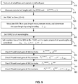
- FIG. 9 is a flow chart of a method for configuring the compensator.
- FIGS. 10-12 illustrate examples of compensator configuration.
- FIG. 1 illustrates a typical Data Center Interconnect (DCI), wherein a plurality of storage and computational devices may be connected to transmitters, receivers, and transceivers, collectively denoted as TRs 130 , and so interconnected via a communication network illustrated by MUX/DEMUX devices 110 and span fiber 120 .
- the optical system may be designed for propagating optical signals with wavelengths from 1528 to 1620 nm, each signal within a particular channel which may be characterized a range ⁇ c ⁇ , wherein ⁇ c is a central wavelength of the channel.
- a typical optical communication system may have remote tails, i.e. optical fibers providing optical signals also referred herein as “light” in one or several but not all channels to or from the system, with unknown lengths in the range of from 0 to 10 km.
- the system may include a 100 G PAM4 transponder, provide 80 GHz bandwidth, and require +/ ⁇ 100 ps chromatic dispersion tolerance.
- the method disclosed herein provides compensation for chromatic dispersion caused by propagation of optical signals in the span fiber 120 as well as for dispersion caused by propagation of the signals in the remote tails 140 , i.e. after the exit MUX.
- the compensation is understood as at least partial compensation.
- the method will be disclosed as performed in the DCI system of FIG. 1 , illustrated in FIG. 3 in more detail.
- the system includes amplifiers such as an amplifier 115 for compensation of insertion loss, a BER monitor 300 , and a Tunable Optical Chromatic Dispersion Compensator (TODC) 310 to compensate the chromatic dispersion.
- amplifiers such as an amplifier 115 for compensation of insertion loss, a BER monitor 300 , and a Tunable Optical Chromatic Dispersion Compensator (TODC) 310 to compensate the chromatic dispersion.
- TODC Tunable Optical Chromatic Dispersion Compensator
- the method includes determining ( 210 ) one or more parameters related to chromatic dispersion in the span fiber.
- the chromatic dispersion in the span fiber or the span fiber length maybe determined using a Bit Error Ratio (BER) measuring unit.
- BER Bit Error Ratio
- the dispersion compensation system includes a close loop chromatic dispersion compensation based on BER monitoring.
- a BER monitor 300 includes tunable transmitter 410 and receiver 420 .
- the BER equipment may be a simple BER estimation unit.
- Random test signals (e.g. 101100001001111100010101010101) are generated by the Tx 410 and sent out.
- a variable optical attenuator (not shown) may adjust the test signal power so that difference OSNR can be achieved, i.e. that the bit error is mainly from the chromatic dispersion not the optical noise, when the signal passes through Mux 111 , EDFA 113 , TODC 117 , span fiber 121 , EDFA 119 , DeMux 110 , Mux 111 , EDFA 123 , span fiber 120 , TODC 125 , EDFA 115 , Demux 110 and back to the BER monitor 300 , to receiver Rx 420 .
- the processor (not shown) of the BER monitor then compares the sent and received signals, and uses the obtained information for controlling the compensator 117 .
- the TRs 410 & 420 used for BER monitoring may also be used for the span length measurement.
- an optical time-domain reflectometer e.g. such as the OTDR 310 described later with reference to FIG. 4
- the length value is then used for controlling the compensator.
- a signal from the Tx 410 within the BER monitor 300 may be used for measuring the span link length.
- the Tx 410 may generate pulse with suitable frequency.
- the time delay between the send time and the receive time depends on the fiber length. By evaluating the bit shift between the sent and received signals, it is possible to find the distance traversed by the signal.
- the signal may be allowed to pass through the span fiber two or more times with the formula for L span adjusted correspondingly.
- the method also includes determining ( 220 ) a remote tail length 140 ( FIG. 1 ), for propagating a particular channel, more precisely a signal with frequencies within a specific range associated with the channel. This is done for each of the plurality of channels, possibly using a broadband optical time-domain reflectometer (OTDR).
- OTDR optical time-domain reflectometer
- a low cost tunable OTDR may be used to detect the remote tail length for each of the channels.
- the remote tails are random from 0 to 10 km, causing CD of 0 to 180 ps.
- the dispersion in the tails may be greater than dispersion tolerance of the Rx at the end of the tail, and so has to be compensated.
- an OTDR 310 may be disposed in front of the exit MUX 110 and receive light from a boost amplifier 115 .
- the OTDR 310 may include a modulator 510 ( FIG. 4 ), a circulator 520 , an optical filter 530 , and a receiver 540 .
- the modulator 510 may be a fast optical switch for cost reduction.
- the modulator 510 may modulate broadband light provided to the OTDR 310 from an amplifier preceding the OTDR in the optical system, the amplifier 115 in this particular example.
- the light may be modulated in the time-domain so as to determine the tail lengths the same way as it has been described for the span fiber length, using the bit delay.
- the light modulated by the modulator 510 is distributed by the Mux 110 (e.g. an Arrayed Waveguide Grating) to different remote tails so as to reach different TRs 130 , wherein the terms “remote tail” and “tail” are used for fibers connecting the exit MUX with end devices illustrated by the transmitters and receivers.
- Some of the light may be reflected back to the circulator 520 from surfaces of each Rx and then selected by the tunable filter 530 .
- the tunable filter 530 scans across the full wavelength range. Delay times for each channel can be measured by comparing the reflected signal with the modulation signal, and determining the bit shift, so as to obtain a remote tail length for each the plurality of channels.
- a remote tail distance may be determined for each wavelength of interest and so for each particular channel in the system, and then used for chromatic dispersion compensation on per channel basis.
- determining ( 210 ) one or more parameters related to chromatic dispersion in the span fiber and determining ( 220 ) remote tail lengths may be performed in any order or in parallel.
- the method also includes compensating ( 230 , FIG. 2 ) the chromatic dispersion of the span fiber and tail chromatic dispersion on per-channel basis using a tunable compensator, wherein the one or more parameters related to chromatic dispersion in the span fiber and the remote tail length for signals in each of the plurality of optical channels are used for controlling the tunable compensator.
- chromatic dispersion compensation There are several technical challenges associated with chromatic dispersion compensation. Most tunable dispersion compensators have insufficient tuning range for accommodating high bandwidth/channel-spacing ratios. Random channel dispersion requires individual channel dispersion compensation. A non-channelized, tunable dispersion compensator based on a wavelength selective switch (WSS) is disclosed herein for chromatic dispersion compensation on per-channel basis.
- WSS wavelength selective switch
- FIG. 5 illustrates an embodiment of the tunable optical dispersion compensator (TODC) 117 for chromatic dispersion (CD) compensation of optical signals in a plurality of optical channels.
- TODC tunable optical dispersion compensator
- CD chromatic dispersion
- the TODC 117 uses dispersion compensation fibers (DCF) known in the industry. When light propagates through a fiber, the velocity is a nonlinear function of the wavelength.
- the TODC 117 includes two groups of DCFs. The first group, formed by one or more DCFs, each connected for propagating and compensating all signals of all channels together, may be thought of as compensating the mean dispersion which happens in the span fiber.
- the chromatic dispersion is almost same for all the channels, and differs from channel to channel due to the slope effect.
- the second group of DCFs is for compensating CD in signals on per-channel basis.
- the DCFs of the second group are designed for compensating the dispersion which happens in tails, and the chromatic dispersion slop mismatch between the span fiber and the DCFs.
- the mean dispersion may be only partially compensated in the DCFs of the first group; a portion of the mean dispersion may be compensated in the DCFs of the second group, on per-channel basis.
- the TODC 117 has a first switch 610 configurable for directing all signals in the plurality of optical channels to a first CD compensation fiber 620 , in a first mode of operation, and for bypassing the first CD compensation fiber 620 when the switch is in a second mode of operation.
- the first fiber 620 represents the first group of fibers.
- the first switch 610 may be a 2 ⁇ 2 switch.
- the TODC 117 includes a tunable optical switch 630 configurable for directing an optical signal in any of the plurality of optical channels to one of the plurality of fibers of the second group, dependent on a central wavelength of the optical signal.
- the second group includes a plurality of optical fibers, illustrated by fibers 641 - 644 .
- the second group may include more than 4 fibers, e.g. 8, 12, 24, 36 fibers.
- the dispersion compensation values associated with the fibers of the second group differ from one another, at least most of them.
- the WSS switch 630 is a 1 ⁇ M wavelength selective switch.
- the WSS 630 switch may be 1 ⁇ 8, 1 ⁇ 9, or 1 ⁇ 16 switch.
- N may be equal to M ⁇ 1 or M ⁇ 2.
- the TODC 117 may also include a fiber mirror 650 for reflecting each signal propagating through a particular fiber of the second group of fibers back into that fiber and further to the fiber(s) of the first group such as the first fiber 620 and a second fiber 660 ( FIG. 6 ), if the switch 610 and switch 670 ( FIG. 6 ) are so configured.
- the circulator 680 Through the circulator 680 , the at least partially compensated signal returns into the optical system.
- the first switch 610 is connected serially with the tunable optical switch 630 , so that all signals of all channels enter and exit the first switch 610 and also enter and exit the tunable switch 630 . That enables combining CD compensation provided by any one of the plurality of optical fibers 641 - 644 and CD compensation provided by the first optical fiber 620 .
- the first and second groups of fibers are distinct in the sense that no fiber belongs to both groups.
- the difference between the first and second groups of compensation fibers is that (1) each fiber of the first group is connected for propagating signals of all channels simultaneously or being bypassed by all signals simultaneously, dependent on the mode of operation of the compensator, whereas (2) each fiber of the second group is connected to a WSS and receives one or more channels dependent on their wavelengths.
- the least of the dispersion values is preferably less than a predefined resolution and each of other dispersion values is greater than its preceding dispersion value by no more than the predefined resolution, when the dispersion values are arranged in increasing order.
- the compensator enables a broad spectrum of compensation values, including the range D 1 to D N , related to the bypassing mode of the first switch, and the range D+D 1 to D+D N .
- the first optical fiber has a dispersion compensation value D such that the greatest of dispersion values D N associated with the plurality of optical fibers in the second group is less than the least of dispersion values formed by adding the dispersion value D associated with the first optical fiber to the dispersion values D 1 . . . D N associated with the plurality of optical fibers by no more than the predefined resolution R.
- D N ⁇ D+D 1 so as to provide continuity between the two ranges of compensation values, which is associated with zero CD compensation tolerance. The higher modulation speed, the lower compensating tolerance.
- FIG. 6 illustrates an embodiment of the compensator 117 .
- a second switch 670 preferably a 2 ⁇ 2 switch, and a second fiber DCF 660 , also for propagating and compensating all signals together.
- the second fiber 660 belongs to the first group of fibers, together with the first fiber 620 . All the switches are connected serially for combining the compensation provided by each fiber of the first group, each fiber of the first group may be used or bypassed, and one of the fibers of the second group, selected dependent on the central wavelength of a signal being compensated.
- FIG. 7 illustrates an embodiment of the compensator 117 .
- the compensator includes an optical combiner 690 , for combining the signals propagating in the plurality of fibers into a broadband signal which will be provided to the optical system; the optical combiner 690 is preferably a WSS, may also be a 1 ⁇ M combiner.
- the second 2 ⁇ 2 switch 670 and the second DCF fiber 660 are optional as discussed with reference to FIGS. 5 and 6 .
- the first group may include fibers associated with compensation values of 200, 400, and 800 ps.
- the variety of combinations of the ten DCF coils forms Chromatic Dispersion compensation values from 0 ps to 1550 ps, which covers 0 to 80 km SMF fiber with 50 ps resolution (1 ⁇ 2 of 25 G PAM4 Chromatic Dispersion tolerance).
- the same lengths of fibers when used in the embodiment of FIG. 5 , will provide compensation values two times higher than in the compensator of FIG. 7 , because of the return path of light through the same fibers.
- the fibers in the compensator shown in FIG. 5 may be twice shorter than in the compensator shown in FIG. 7 , though providing the same compensation.
- the dispersion compensation fibers are preferably selected so as to compensate both the chromatic dispersion in the span and tails and chromatic dispersion slop match as much as possible, or at least with a predefined accuracy.
- a first switch 710 may direct all signals propagating in the plurality of optical channels to one of the optical fibers 741 - 744 , which belong to the first group of fibers, i.e. each is used for compensation of all the channels simultaneously.
- all the channels are directed to a first fiber 741 , and the fibers 742 - 744 are bypassed.
- all the channels are directed to a second fiber 742 , while the first fiber 741 and fibers 743 and 744 are bypassed, and so on.
- the first switch 710 may be a configurable 1 ⁇ M 1 switch, i.e. have M 1 output ports. While FIG.
- the compensator illustrated in FIG. 7A has a switch 630 , which is a tunable optical switch, configurable for directing an optical signal in any of the plurality of optical channels to one of the plurality of fibers of the second group, dependent on a central wavelength of the optical signal.
- the WSS 630 is configured on per-channel basis, for directing each channel to a particular port connected to a corresponding fiber of the second group, though it is possible that two channels may be directed to a same output port.
- the compensator illustrated in FIG. 7A has another switch 690 for combining all the channels together into a broadband signal, as in FIG. 7 .
- the combiner 690 is optional and may be replaced with a mirror such as the mirror 650 ( FIG. 6 ).
- the mirror 750 is optional, and may be replaced with another 1 ⁇ M 1 switch (not shown), the same way as the switch 690 ( FIG. 7 ) replaces the mirror 650 ( FIG. 6 ).
- the first switch ( 610 or 710 ), the optional second switch 670 , and the WSS 630 are connected so as to enable combining CD compensation provided by any one fiber of the second group ( 640 , 641 - 644 ) and CD compensation provided by any fiber of the first group, e.g. the first optical fiber ( 620 , 741 ), e.g. the switches are connected serially as illustrated in FIGS. 5-7A .
- the compensator provides dispersion compensation in each particular channel, taking into account the remote tail of that channel. Additionally, using compensation fibers of the first group for compensating all the channels together requires significantly less compensation fiber than it would be used in separate compensators each for a particular channel.
- the method and the compensator disclosed herein may be used for compensating chromatic dispersion for optical signals in the range of wavelengths from 1528 to 1620 nm.
- the method may be implemented in a chromatic dispersion compensation system, within an optical communication system such as DCI illustrated in FIG. 3 .
- the dispersion compensation system includes a BER measurement unit also referred to as a BER monitor 300 , and an optical time-domain reflectometer (OTDR) 310 , both for estimating dispersion in the span and tail fiber, respectively.
- a BER monitor 300 also referred to as a BER monitor 300
- OTDR optical time-domain reflectometer
- the BER monitor 300 and the OTDR 310 share the use of the transmitter 410 and receiver 420 .
- the compensation system further includes a tunable dispersion compensator (TODC) 117 for compensating the span and tail dispersion.
- TODC tunable dispersion compensator
- the compensation system also includes a control subsystem for controlling and coordinating the BER measurement unit, the OTDR, and the TODC, wherein the TODC provides dispersion compensation based on the measurements performed by the BER and OTDR units.
- the control subsystem of the chromatic dispersion compensation system may include one or more hardware microprocessors, FPGA and/or ASIC logic.
- the control subsystem may control the tunable transmitter of the BER equipment and the tunable optical filter of the OTDR, collect their data, and use the data for configuring the compensator.
- the control system may include computer readable memory with instructions stored therein; the instructions when executed cause the one or more microprocessors to implement the method.
- Provisioning, or setting the configuration, of the chromatic dispersion compensator in an optical system will be discussed with reference to FIGS. 8 and 9 .
- FIG. 8 illustrates power budget and amplifier gain in the optical system discussed above with reference to FIG. 3 , wherein equipment constants and parameters to be achieved in operation include:
- P 1 is the input power to the input port of amplifier BA 11 .
- P 2 is the power from amp BA 12 , the power launch to transform fiber
- P 3 is the input power to the input port of amplifier PA 1 ,
- P 4 is the output power from the output port of amplifier PA 1 ,
- P 5 is the input power to the input port of amplifier BA 2 .
- P 7 is the input power to the input port of amplifier PA 21 .
- P 8 is the output power from the output port of amplifier PA 22 .
- P tx is output power of the Tx
- P rx is receiving power of the Rx
- IL mux is insertion loss of the Mux/Demux
- IL span is insertion loss of span fiber.
- FIG. 9 illustrates one embodiment of the method discussed above with reference to FIG. 2 .
- the provisioning steps are shown in FIG. 9 , and include operating ( 910 ) the optical system in predetermined amplifier gain according to the designed span length while all amplifiers are turned on, and measuring ( 915 ) remote tail lengths with the OTDR unit 310 , for each channel.
- the method also includes setting ( 920 ) TODC 117 to a least possible value, i.e. as close to zero as possible.
- a least possible value i.e. as close to zero as possible.
- the first switch 710 may be configured to direct all optical signals to the compensation fiber of the first group which would provide the least compensation value, the fiber 741 , and set the WSS 630 to switch all the wavelengths to port 1 connected to a compensation fiber associated with the least compensation value among the fibers of the second group, DSF 1 .
- the method includes span length measurement (or estimation) using the BER unit.
- the modulation frequency of TX 410 should be much lower than in the BER measuring mode to achieve proper distance resolution and measurement range.
- the provisioning also includes modulating ( 925 ) the BER Tx in BER monitoring mode, and performing span CD estimation.
- the BER TR/Tx 410 is preferably tunable across all channels.
- the BER TR/Tx 410 transmits and modulates the light in the span length measurement mode, and determines the span length using the bit delay as discussed above so as to obtain L span .
- the signal from Tx 410 for CD estimation should be more sensitive to the CD tolerance than the system signal, for example, have higher modulation frequency or wider bandwidth.
- Random test signals (e.g. 101100001001111100010101010101) from Tx 410 passes through Mux 111 , EDFA 113 , TODC 117 , span fiber 121 , EDFA 119 , DeMux 110 , Mux 111 , EDFA 123 , span fiber 120 , TODC 125 , EDFA 115 , Demux 110 and back to the BER monitor 300 , to receiver Rx 420 .
- the received signal and sent signal then be compared and BER (bit error rate) is estimated (in ideal case i.e. zero CD tolerance, the BER should be zero).
- the measured BER then be used to adjust compensator 117 , until minimum BER value is achieved or approximated with a predefined accuracy.
- the provisioning further includes setting ( 935 ) TODC for all wavelengths corresponding to signals in all channels propagating in the system.
- FIG. 11 illustrates setting ( 935 ) the TODC for the above example.
- determining ( 210 ) one or more parameters related to chromatic dispersion in the span fiber corresponds to step 925 ( FIG. 9 ), and determining ( 220 ) a remote tail length for each of the plurality of optical channels corresponds to step 915 ( FIG. 9 ).
- Steps 925 - 960 relate to configuring the compensator 117 , including configuring the first switch 610 or 710 , the WSS 630 , and the optional second switch 670 , for the compensator 117 , in operation, to compensate ( 230 , FIG. 2 ) the chromatic dispersion of the span fiber and tail chromatic dispersion on per-channel basis. All or at least some of the method steps may be performed using the control subsystem.
Landscapes
- Physics & Mathematics (AREA)
- Electromagnetism (AREA)
- Engineering & Computer Science (AREA)
- Computer Networks & Wireless Communication (AREA)
- Signal Processing (AREA)
- Optical Communication System (AREA)
Abstract
Description
G BA1 =G BA11 −IL TODC +G BA12
G PA2 =G PA21 −IL TODC +G PA22
Claims (14)
Priority Applications (1)
| Application Number | Priority Date | Filing Date | Title |
|---|---|---|---|
| US16/410,879 US11044019B2 (en) | 2018-05-11 | 2019-05-13 | Method and device for chromatic dispersion compensation |
Applications Claiming Priority (2)
| Application Number | Priority Date | Filing Date | Title |
|---|---|---|---|
| US201862670257P | 2018-05-11 | 2018-05-11 | |
| US16/410,879 US11044019B2 (en) | 2018-05-11 | 2019-05-13 | Method and device for chromatic dispersion compensation |
Publications (2)
| Publication Number | Publication Date |
|---|---|
| US20190349092A1 US20190349092A1 (en) | 2019-11-14 |
| US11044019B2 true US11044019B2 (en) | 2021-06-22 |
Family
ID=68464365
Family Applications (1)
| Application Number | Title | Priority Date | Filing Date |
|---|---|---|---|
| US16/410,879 Active US11044019B2 (en) | 2018-05-11 | 2019-05-13 | Method and device for chromatic dispersion compensation |
Country Status (1)
| Country | Link |
|---|---|
| US (1) | US11044019B2 (en) |
Cited By (1)
| Publication number | Priority date | Publication date | Assignee | Title |
|---|---|---|---|---|
| US20220390321A1 (en) * | 2021-06-04 | 2022-12-08 | Exfo Inc. | Spectral averaging of otdr traces |
Families Citing this family (3)
| Publication number | Priority date | Publication date | Assignee | Title |
|---|---|---|---|---|
| US11243356B2 (en) * | 2017-07-21 | 2022-02-08 | Telefonaktiebolaget Lm Ericsson (Publ) | Chromatic dispersion compensation |
| US11290184B2 (en) * | 2019-03-01 | 2022-03-29 | Molex, Llc | Switchable dispersion compensating module |
| US11652547B2 (en) * | 2021-09-24 | 2023-05-16 | Huawei Technologies Co., Ltd. | Method and systems to identify types of fibers in an optical network |
Citations (14)
| Publication number | Priority date | Publication date | Assignee | Title |
|---|---|---|---|---|
| US5602666A (en) * | 1993-08-10 | 1997-02-11 | Fujitsu Limited | Optical dispersion compensation method for shifting a zero dispersion wavelength of an optical fiber to compensate for dispersion in an optical system |
| US20020015207A1 (en) * | 2000-08-07 | 2002-02-07 | Hiroki Ooi | Method and system for compensating chromatic dispersion |
| US6466341B1 (en) * | 1998-08-03 | 2002-10-15 | Agere Systems Guardian Corp. | Add/drop filter for a multi-wavelength lightwave system |
| US20030002772A1 (en) * | 2001-06-13 | 2003-01-02 | Makoto Katayama | Variable dispersion compensator and optical transmission system |
| US20030169967A1 (en) * | 2000-06-30 | 2003-09-11 | Pierre Sillard | Chromatic dispersion compensation in a broadband optical transmission system |
| US20060051039A1 (en) * | 2004-07-02 | 2006-03-09 | Haiqing Wei | Nonlinearity compensation in a fiber optic communications system |
| US20060067700A1 (en) * | 2004-09-28 | 2006-03-30 | Nec Corporation | Wavelength division multiplexing optical transmission system and wavelength division multiplexing optical transmission method |
| US20060133815A1 (en) * | 2004-12-17 | 2006-06-22 | Yasuyuki Fukashiro | Dispersion compensation device and dispersion compensation method |
| US20060193556A1 (en) * | 2005-02-28 | 2006-08-31 | Engana Pty Ltd. Of Locomotive Workshop | Optical communications system |
| US20070015969A1 (en) * | 2005-06-06 | 2007-01-18 | Board Of Regents, The University Of Texas System | OCT using spectrally resolved bandwidth |
| US20070223926A1 (en) * | 2004-12-27 | 2007-09-27 | Yasuyuki Fukashiro | Dispersion compensation device and dispersion compensation method |
| US20080151377A1 (en) * | 2006-12-20 | 2008-06-26 | Kenro Sekine | Dispersion compensator, optical transmission system and optical transmission method |
| US20090060523A1 (en) * | 2007-08-27 | 2009-03-05 | Lijie Qiao | In-service optical dispersion determining system and method |
| US10225016B1 (en) * | 2016-06-28 | 2019-03-05 | Amazon Technologies, Inc. | Optical power and chromatic dispersion equalization system |
-
2019
- 2019-05-13 US US16/410,879 patent/US11044019B2/en active Active
Patent Citations (15)
| Publication number | Priority date | Publication date | Assignee | Title |
|---|---|---|---|---|
| US5602666A (en) * | 1993-08-10 | 1997-02-11 | Fujitsu Limited | Optical dispersion compensation method for shifting a zero dispersion wavelength of an optical fiber to compensate for dispersion in an optical system |
| US5636046A (en) * | 1993-08-10 | 1997-06-03 | Fujitsu Limited | Optical dispersion compensation method using transmissible band determined from synergetic effect of self phase modulation and group velocity dispersion |
| US6466341B1 (en) * | 1998-08-03 | 2002-10-15 | Agere Systems Guardian Corp. | Add/drop filter for a multi-wavelength lightwave system |
| US20030169967A1 (en) * | 2000-06-30 | 2003-09-11 | Pierre Sillard | Chromatic dispersion compensation in a broadband optical transmission system |
| US20020015207A1 (en) * | 2000-08-07 | 2002-02-07 | Hiroki Ooi | Method and system for compensating chromatic dispersion |
| US20030002772A1 (en) * | 2001-06-13 | 2003-01-02 | Makoto Katayama | Variable dispersion compensator and optical transmission system |
| US20060051039A1 (en) * | 2004-07-02 | 2006-03-09 | Haiqing Wei | Nonlinearity compensation in a fiber optic communications system |
| US20060067700A1 (en) * | 2004-09-28 | 2006-03-30 | Nec Corporation | Wavelength division multiplexing optical transmission system and wavelength division multiplexing optical transmission method |
| US20060133815A1 (en) * | 2004-12-17 | 2006-06-22 | Yasuyuki Fukashiro | Dispersion compensation device and dispersion compensation method |
| US20070223926A1 (en) * | 2004-12-27 | 2007-09-27 | Yasuyuki Fukashiro | Dispersion compensation device and dispersion compensation method |
| US20060193556A1 (en) * | 2005-02-28 | 2006-08-31 | Engana Pty Ltd. Of Locomotive Workshop | Optical communications system |
| US20070015969A1 (en) * | 2005-06-06 | 2007-01-18 | Board Of Regents, The University Of Texas System | OCT using spectrally resolved bandwidth |
| US20080151377A1 (en) * | 2006-12-20 | 2008-06-26 | Kenro Sekine | Dispersion compensator, optical transmission system and optical transmission method |
| US20090060523A1 (en) * | 2007-08-27 | 2009-03-05 | Lijie Qiao | In-service optical dispersion determining system and method |
| US10225016B1 (en) * | 2016-06-28 | 2019-03-05 | Amazon Technologies, Inc. | Optical power and chromatic dispersion equalization system |
Cited By (2)
| Publication number | Priority date | Publication date | Assignee | Title |
|---|---|---|---|---|
| US20220390321A1 (en) * | 2021-06-04 | 2022-12-08 | Exfo Inc. | Spectral averaging of otdr traces |
| US12050150B2 (en) * | 2021-06-04 | 2024-07-30 | Exfo Inc. | Spectral averaging of OTDR traces |
Also Published As
| Publication number | Publication date |
|---|---|
| US20190349092A1 (en) | 2019-11-14 |
Similar Documents
| Publication | Publication Date | Title |
|---|---|---|
| US11044019B2 (en) | Method and device for chromatic dispersion compensation | |
| US11201667B2 (en) | Optical fiber characterization measurement systems and methods | |
| US7489880B2 (en) | Apparatus and method for measuring the dispersion of a fiber span | |
| US5923453A (en) | Apparatus for measuring optical transmission line property and optical wavelength multiplexing transmission apparatus | |
| US8073325B2 (en) | OSNR measuring apparatus and OSNR measuring method | |
| US6907197B2 (en) | Method and apparatus for measuring and estimating optical signal to noise ratio in photonic networks | |
| US9140624B2 (en) | Systems and methods reducing coherence effect in narrow line-width light sources | |
| US20020154372A1 (en) | Power and optical frequency monitoring system and transmission system of frequency-modulated optical signal | |
| EP0924888A2 (en) | Method and apparatus for channel equalization in wavelength division multiplexed systems | |
| US7912370B2 (en) | Optical power measurement apparatus and optical power measurement method | |
| US20230152183A1 (en) | Fiber Span Characterization Utilizing Paired Optical Time Domain Reflectometers | |
| JP2002508622A (en) | Method and apparatus for reducing four-wave mixing | |
| US9638574B2 (en) | Measurement apparatus and method of measuring signal light quality | |
| EP3758258B1 (en) | Measuring linear and non-linear transmission perturbations in optical transmission systems | |
| US7257324B2 (en) | Apparatus for monitoring optical signal-to-noise ratio | |
| US9166691B2 (en) | Method for coupling an emitting device to a frequency splitter in an optical passive network | |
| US6842561B2 (en) | Optical performance monitoring scheme | |
| US10432303B2 (en) | Method and apparatus for providing a pilot tone | |
| US8768165B2 (en) | Method and arrangement for in service Raman gain measurement and monitoring | |
| US20090269058A1 (en) | System and Method for Self-Generation of Reference Signals | |
| Nivethitha et al. | Performance analysis of photonic crystal ring resonator demultiplexer in DWDM system | |
| US7298464B1 (en) | System and method for measuring the phase noise of very long fiber optic links | |
| JPH1062570A (en) | Method and apparatus for measuring time lag | |
| US8139952B2 (en) | System and method for measuring the extinction ratio of an optical transmitter using an interferogram wing-to-peak ratio | |
| Chen et al. | Global Power and OSNR Analyses for Super C band Optical Transmission Systems |
Legal Events
| Date | Code | Title | Description |
|---|---|---|---|
| FEPP | Fee payment procedure |
Free format text: ENTITY STATUS SET TO UNDISCOUNTED (ORIGINAL EVENT CODE: BIG.); ENTITY STATUS OF PATENT OWNER: LARGE ENTITY |
|
| STPP | Information on status: patent application and granting procedure in general |
Free format text: DOCKETED NEW CASE - READY FOR EXAMINATION |
|
| STPP | Information on status: patent application and granting procedure in general |
Free format text: NON FINAL ACTION MAILED |
|
| STPP | Information on status: patent application and granting procedure in general |
Free format text: RESPONSE TO NON-FINAL OFFICE ACTION ENTERED AND FORWARDED TO EXAMINER |
|
| STPP | Information on status: patent application and granting procedure in general |
Free format text: NOTICE OF ALLOWANCE MAILED -- APPLICATION RECEIVED IN OFFICE OF PUBLICATIONS |
|
| STPP | Information on status: patent application and granting procedure in general |
Free format text: PUBLICATIONS -- ISSUE FEE PAYMENT VERIFIED |
|
| STCF | Information on status: patent grant |
Free format text: PATENTED CASE |
|
| AS | Assignment |
Owner name: ACCELINK TECHNOLOGIES CO., LTD., CHINA Free format text: ASSIGNMENT OF ASSIGNORS INTEREST;ASSIGNOR:BU, QINLIAN;REEL/FRAME:063205/0401 Effective date: 20221205 Owner name: ACCELINK TECHNOLOGIES CO., LTD, CHINA Free format text: ASSIGNMENT OF ASSIGNORS INTEREST;ASSIGNOR:XIAO, LI;REEL/FRAME:063206/0575 Effective date: 20221205 Owner name: GC PHOTONICS INC., CANADA Free format text: ASSIGNMENT OF ASSIGNORS INTEREST;ASSIGNOR:QIAO, LIJIE;REEL/FRAME:063205/0124 Effective date: 20221218 |
|
| AS | Assignment |
Owner name: ACCELINK TECHNOLOGIES CO., LTD., CHINA Free format text: ASSIGNMENT OF ASSIGNORS INTEREST;ASSIGNOR:GC PHOTONICS INC.;REEL/FRAME:063215/0608 Effective date: 20221218 |
|
| MAFP | Maintenance fee payment |
Free format text: PAYMENT OF MAINTENANCE FEE, 4TH YEAR, LARGE ENTITY (ORIGINAL EVENT CODE: M1551); ENTITY STATUS OF PATENT OWNER: LARGE ENTITY Year of fee payment: 4 |