US11032505B2 - Ramp signal generator and CMOS image sensor using the same - Google Patents
Ramp signal generator and CMOS image sensor using the same Download PDFInfo
- Publication number
- US11032505B2 US11032505B2 US16/219,826 US201816219826A US11032505B2 US 11032505 B2 US11032505 B2 US 11032505B2 US 201816219826 A US201816219826 A US 201816219826A US 11032505 B2 US11032505 B2 US 11032505B2
- Authority
- US
- United States
- Prior art keywords
- ramp signal
- reference voltage
- slope
- controllable
- circuit
- Prior art date
- Legal status (The legal status is an assumption and is not a legal conclusion. Google has not performed a legal analysis and makes no representation as to the accuracy of the status listed.)
- Active, expires
Links
Images


Classifications
-
- H—ELECTRICITY
- H04—ELECTRIC COMMUNICATION TECHNIQUE
- H04N—PICTORIAL COMMUNICATION, e.g. TELEVISION
- H04N25/00—Circuitry of solid-state image sensors [SSIS]; Control thereof
- H04N25/60—Noise processing, e.g. detecting, correcting, reducing or removing noise
- H04N25/67—Noise processing, e.g. detecting, correcting, reducing or removing noise applied to fixed-pattern noise, e.g. non-uniformity of response
- H04N25/671—Noise processing, e.g. detecting, correcting, reducing or removing noise applied to fixed-pattern noise, e.g. non-uniformity of response for non-uniformity detection or correction
-
- H04N5/37455—
-
- H—ELECTRICITY
- H04—ELECTRIC COMMUNICATION TECHNIQUE
- H04N—PICTORIAL COMMUNICATION, e.g. TELEVISION
- H04N25/00—Circuitry of solid-state image sensors [SSIS]; Control thereof
- H04N25/70—SSIS architectures; Circuits associated therewith
- H04N25/76—Addressed sensors, e.g. MOS or CMOS sensors
-
- H—ELECTRICITY
- H10—SEMICONDUCTOR DEVICES; ELECTRIC SOLID-STATE DEVICES NOT OTHERWISE PROVIDED FOR
- H10F—INORGANIC SEMICONDUCTOR DEVICES SENSITIVE TO INFRARED RADIATION, LIGHT, ELECTROMAGNETIC RADIATION OF SHORTER WAVELENGTH OR CORPUSCULAR RADIATION
- H10F39/00—Integrated devices, or assemblies of multiple devices, comprising at least one element covered by group H10F30/00, e.g. radiation detectors comprising photodiode arrays
- H10F39/10—Integrated devices
- H10F39/12—Image sensors
- H10F39/18—Complementary metal-oxide-semiconductor [CMOS] image sensors; Photodiode array image sensors
- H10F39/182—Colour image sensors
-
- H01L27/14645—
-
- H—ELECTRICITY
- H04—ELECTRIC COMMUNICATION TECHNIQUE
- H04N—PICTORIAL COMMUNICATION, e.g. TELEVISION
- H04N25/00—Circuitry of solid-state image sensors [SSIS]; Control thereof
- H04N25/70—SSIS architectures; Circuits associated therewith
- H04N25/709—Circuitry for control of the power supply
-
- H—ELECTRICITY
- H04—ELECTRIC COMMUNICATION TECHNIQUE
- H04N—PICTORIAL COMMUNICATION, e.g. TELEVISION
- H04N25/00—Circuitry of solid-state image sensors [SSIS]; Control thereof
- H04N25/70—SSIS architectures; Circuits associated therewith
- H04N25/76—Addressed sensors, e.g. MOS or CMOS sensors
- H04N25/77—Pixel circuitry, e.g. memories, A/D converters, pixel amplifiers, shared circuits or shared components
-
- H—ELECTRICITY
- H04—ELECTRIC COMMUNICATION TECHNIQUE
- H04N—PICTORIAL COMMUNICATION, e.g. TELEVISION
- H04N25/00—Circuitry of solid-state image sensors [SSIS]; Control thereof
- H04N25/70—SSIS architectures; Circuits associated therewith
- H04N25/76—Addressed sensors, e.g. MOS or CMOS sensors
- H04N25/7795—Circuitry for generating timing or clock signals
-
- H—ELECTRICITY
- H04—ELECTRIC COMMUNICATION TECHNIQUE
- H04N—PICTORIAL COMMUNICATION, e.g. TELEVISION
- H04N25/00—Circuitry of solid-state image sensors [SSIS]; Control thereof
- H04N25/70—SSIS architectures; Circuits associated therewith
- H04N25/76—Addressed sensors, e.g. MOS or CMOS sensors
- H04N25/78—Readout circuits for addressed sensors, e.g. output amplifiers or A/D converters
-
- H04N5/3765—
-
- H04N5/378—
-
- H04N9/045—
Definitions
- CMOS complementary metal oxide semiconductor
- an image sensing device includes pixels for capturing images using photodiodes (PD) that converts light into an electrical current and transfer it to a floating diffusion node, which is an input node (a gate terminal) of a conversion transistor (a source follower transistor), through a transfer transistor.
- PD photodiodes
- the electric current transferred to the floating diffusion node may shift the voltage at an output terminal of the conversion transistor, and this output voltage is called a pixel signal.
- exposure linearity tests are conducted to check linearity of an analog-to-digital conversion code while increasing the amount of light incident on the photodiode of the pixel.
- the non-linearity occurs in the process of transferring the electrical current generated by the photodiode to the floating diffusion node.
- a code error occurs in the process of finding a position of a pixel signal based on the ramp signal.
- An acceptable error rate for a code error is typically around 1%, but those non-linearity issues may cause the code error range to exceed the acceptable error rate.
- the code error range could exceed the acceptable error rate when the pixel signal has a high amplitude.
- This patent document provides, among others, designs of image sensing devices that have a ramp signal generator for adjusting a slope of a ramp signal by adjusting a current of a unit current cell to adjust a step size, unlike another ramp signal generator in which a step size of a unit current cell is fixed.
- This patent document also provides designs of image sensing devices that have a ramp signal generator that minimizes a code error by nonlinearly adjusting a slope of a ramp signal similarly to nonlinearity of a pixel signal.
- a device including a ramp signal generator which may comprise: a slope control circuit configured to generate a controllable analog reference voltage according to a digital setting code value to control a slope of a ramp signal; and at least one unit current cell configured to adjust the slope of the ramp signal by adjusting a current flowing through the at least one unit current cell according to the controllable analog reference voltage generated by the slope control circuit.
- the slope control circuit may comprise: a code providing circuit configured to provide the digital setting code value; and a controllable reference voltage generation circuit configured to generate the controllable analog reference voltage according to the digital setting code value provided by the code providing circuit.
- the code providing circuit may further comprise: a buffer configured to apply to the at least one unit current cell the controllable analog reference voltage generated by the controllable reference voltage generation circuit.
- the buffer may include a source follower circuit.
- the code providing circuit may comprise: a memory configured to receive the digital setting code value from an external image signal processor (ISP), store the digital setting code value, and provide the digital setting code value to the controllable reference voltage generation circuit.
- the controllable reference voltage generation circuit may include a digital-to-analog converter (DAC). A level of an ON/OFF voltage of the at least one unit current cell may be adjusted according to the controllable analog reference voltage generated by the slope control circuit.
- the ramp signal generator may adjust the slope of the ramp signal by adjusting a current flowing through the at least one unit current cell.
- a device including a CMOS image sensor which may comprise: a pixel array configured to include an array of photosensing pixels in rows and columns to output a pixel signal corresponding to incident light; a row decoder configured to select and control pixels in the pixel array according to row lines coupled to rows of photosensing pixels; a ramp signal generator configured to adjust a slope of a ramp signal by adjusting a channel current flowing through an analog switch device based on an analog voltage that may be adjustable in response to a digital code; a comparison circuit configured to compare the ramp signal applied from the ramp signal generator with each pixel signal of the pixel array; a counting circuit configured to count a number of clock pulses according to each output signal of the comparison circuit; a memory circuit configured to store counting information of the counting circuit including the number of clock pulses provided by the counting unit; a control circuit configured to control operations of the row decoder, the ramp signal generator, the comparison circuit, the counting circuit, and the memory circuit; and a column readout circuit configured to output data
- the ramp signal generator may comprise: a slope control circuit configured to generate a controllable analog reference voltage according to a digital setting code value to adjust the slope of the ramp signal; and at least one unit current cell configured to adjust the slope of the ramp signal according to the controllable analog reference voltage generated by the slope control circuit.
- the slope control circuit may comprise: a code providing circuit configured to provide the digital setting code value; and a controllable reference voltage generation circuit configured to generate the controllable analog reference voltage according to the digital setting code value provided by the code providing circuit.
- the code providing circuit may further comprise: a buffer configured to apply to the at least one unit current cell the controllable reference voltage of the controllable reference voltage generation circuit.
- the buffer include a source follower circuit.
- the code providing circuit may comprise: a memory configured to receive the digital setting code value from an external image signal processor (ISP), store the digital setting code value, and provide the digital setting code value to the controllable reference voltage generation circuit.
- the controllable reference voltage generation circuit may include a digital-to-analog converter (DAC).
- a level of an ON/OFF voltage of the at least one unit current cell may be adjusted according to the controllable analog reference voltage generated by the slope control circuit.
- the ramp signal generator may adjust the slope of the ramp signal by adjusting a current flowing through the at least one unit current cell.
- a device including a ramp signal generator which may comprise: a unit current cell including a current path that allows an electrical current constituting a ramp signal to flow from a ramp supply voltage terminal to a ramp resistor, the current path including an analog switch device coupled between the ramp supply voltage terminal and the ramp resistor; and a slope control circuit coupled to the analog switch device and configured to receive a digital setting code value and generate a controllable analog reference voltage in response to the digital setting code value to apply the controllable analog reference voltage to the analog switch device to control a slope of a ramp signal.
- the unit current cell may adjust the slope of the ramp signal by adjusting a channel current flowing through the analog switch device based on the controllable analog reference voltage, which may be adjustable in response to the digital setting code value.
- the slope control circuit may include a digital-to-analog converter (DAC) that converts the digital setting code value to the controllable analog reference voltage.
- DAC digital-to-analog converter
- a ramp signal generator may include a slope control block that generates a controllable reference voltage according to a setting code value and control a slope of a ramp signal, and at least one unit current cell that adjusts the slope of the ramp signal according to the controllable reference voltage of the slope control block.
- a CMOS image sensor may include a pixel array that outputs a pixel signal corresponding to incident light, a row decoder that selects and controls pixels in the pixel array according to row lines, a ramp signal generator that generates a controllable reference voltage according to a setting code value, adjusts a slope of a ramp signal according to the generated controllable reference voltage, and generates the ramp signal, a comparison unit that compares the ramp signal applied from the ramp signal generator and each pixel signal of the pixel array with each other, a counting unit that counts a clock according to each output signal of the comparison unit, a memory unit that stores counting information of the counting unit, a control unit that controls operations of the row decoder, the ramp signal generator, the comparison unit, the counting unit, and the memory unit, and a column readout circuit that outputs data of the memory unit under control of the control unit.
- a current of a unit current cell is adjusted to adjust a step size, so that it is possible to adjust a slope of a ramp signal.
- the slope of the ramp signal is nonlinearly adjusted similarly to non-linearity of a pixel signal, so that it is possible to minimize a code error.
- FIG. 1 is an example diagram of a CMOS image sensor for facilitating the understanding of the disclosed technology.
- FIG. 2A and FIG. 2B are example diagrams of a ramp signal generator for facilitating the understanding of the disclosed technology.
- FIG. 3 is a diagram for explaining an example of a unit current cell array structure of a ramp signal generator based on an embodiment of the disclosed technology.
- FIG. 4A to FIG. 4C are diagrams for explaining an operation of a unit current cell of a ramp signal generator implemented based on an embodiment of the disclosed technology.
- FIG. 5 is a diagram illustrating an example of a ramp voltage based on an embodiment of the disclosed technology.
- FIG. 6 is a configuration diagram of an example of a ramp signal generator implemented based on an embodiment of the disclosed technology.
- FIG. 7 is a diagram illustrating another example ramp signal generator that globally applies an ON/OFF voltage based on an embodiment of the disclosed technology.
- FIG. 8 is a configuration diagram of an example of a CMOS image sensor implemented based on an embodiment of the disclosed technology.
- FIG. 1 is an example diagram of a CMOS image sensor (CIS) for facilitating the understanding of the disclosed technology, and illustrates a CMOS image sensor having a column parallel structure implemented using a general single slope analog-to-digital converter.
- CIS CMOS image sensor
- the CMOS image sensor includes a pixel array 10 of photosensing pixels arranged in rows and columns to respond to incident light to output a pixel signal.
- Each photosensing pixel may be implemented by a photo diode, a photo transistor, a photo gate, or other photosensitive circuitry capable of converting light into a pixel signal (e.g., a charge, a voltage or a current).
- an array of different color filters are placed to cover the photosensing pixels to filter the incident light in different colors at different pixel locations to capture the color information in a sensed image. The specific example in FIG.
- the CMOS image sensor also includes a row decoder 20 , a ramp signal generator 30 , a comparison unit (comparison circuit) 40 , a counting unit (counting circuit) 50 , a memory unit (memory circuit) 60 , a control unit (control circuit) 80 , and a column readout circuit 70 .
- the row decoder 20 selects pixels in the pixel array 10 according to row lines and controls operations of the pixels according to instructions provided by the control unit 80 .
- the ramp signal generator 30 generates a ramp signal according to instructions provided by the control unit 80 .
- the comparison unit 40 compares a value of the ramp signal applied from the ramp signal generator 30 with values of each pixel signal outputted from the pixel array 10 according to instructions provided by the control unit 80 .
- the counting unit 50 counts the number of clock pulses of the control unit 80 according to each output signal of the comparison unit 40 .
- the memory unit 60 stores counting information including the number of clock pulses provided by the counting unit 50 under the control of the control unit 80 .
- the control unit 80 controls the operations of the row decoder 20 , the ramp signal generator 30 , the comparison unit 40 , the counting unit 50 , the memory unit 60 , and the column readout circuit 70 .
- the column readout circuit 70 sequentially outputs data of the memory unit 60 as pixel data PXDATA according to instructions provided by the control unit 80 .
- a CMOS image sensor may use the correlated double sampling (CDS) to remove an offset value of pixels by sampling a pixel signal twice so that the difference is taken between these two samples.
- the correlated double sampling (CDS) may remove an offset value of pixels by comparing pixel signals (pixel output voltages) obtained before and after light is incident on the pixels with each other, so that only pixel signals based on the incident light can be actually measured.
- the CDS may be conducted by the comparison unit 40 .
- the comparison unit 40 includes a plurality of comparators, the counting unit 50 includes a plurality of counters, and the memory unit 60 includes a plurality of memories.
- each column of the pixel array 10 includes, the comparators, the counters, and the memories.
- a first comparator 41 has two input terminals including one terminal that receives a pixel signal outputted from a first column of the pixel array 10 , and the other terminal that receives a ramp signal applied from the ramp signal generator 30 .
- the first comparator 41 compares values of the two signals (pixel signal and ramp signal) with each other according to a control signal of the control unit 80 , and outputs a comparison signal.
- Examples of the ramp signal V RAMP include a signal whose voltage level decreases or increases, a saw-tooth signal, and other types of reference signals. When the voltage of the ramp signal matches that of the pixel signal at a certain time point, values of comparison signals outputted from each comparator are inverted.
- a first comparator 51 counts clock pulses provided by the control unit 80 until the comparison signal outputted from the comparator 41 is inverted from the time point at which the ramp signal starts to fall, and outputs counting information regarding the number of clock pulses counted by the first comparator 51 .
- the respective counters are initialized according to a reset control signal from the control unit 80 .
- a first memory 61 stores the counting information regarding the number of clock pulses counted by the first comparator 51 according to a load control signal of the control unit 80 , and outputs the counting information to the column readout circuit 70 .
- counting is performed on a reset signal (a reset voltage) and then is performed on an image signal (a signal voltage).
- FIG. 2A and FIG. 2B are example diagrams of a ramp signal generator for facilitating the understanding of the disclosed technology.
- the ramp signal generator includes a unit current cell array and a ramp resistor R L , which is a common node electrically connected to the unit current cell array in common.
- a ramp voltage V RAMP is generated according to Equation 1 below.
- V RAMP I TOTAL *R L (Equation 1)
- I TOTAL denotes the total electric current flowing in all the unit current cells.
- an initial state of a ramp voltage is that a PMOS transistor MP R2 stays “off” (e.g., a switch SW RB stays off and a switch SW R stays on) so that currents can flow through all unit current cells (i.e., through all PMOS transistors MPR 1 ) to the ramp resistor R L as illustrated in FIG. 2A .
- the switch SW RB and the switch SW R may be provided between the ramp supply voltage terminal and a ground voltage terminal to be turned on or off in response to control signals provided by the control unit 80 of FIG. 1 or control signals provided by another controller (not illustrated) operating by receiving clock signals from the control unit 80 of FIG. 1 .
- the switch SW RB and the switch SW R may be configured to control gate voltages of the PMOS transistor MP R1 and the PMOS transistor MP R2 . As illustrated in FIG. 2B , after the initial state above the unit current cells start to change their current paths from the PMOS transistor MPR 1 to the PMOS transistor MPR 2 .
- the PMOS transistor MP R1 is turned off and the PMOS transistor MP R2 is turned on (the switch SW RB is turned on and the switch SW R is turned off), and the unit current cells sequentially (one by one) allow the current to flow to the PMOS transistor MP R2 instead of the PMOS transistor MPR 1 .
- the ramp voltage can be expressed by Equation 2 below.
- V RAMP ( I TOTAL ⁇ I T_off )* R L (Equation 2)
- I T_off denotes the amount of the current reduced from the total sum I TOTAL of current by changing the current paths of the unit current cells from the PMOS transistor M PR1 to the PMOS transistor M PR2 such that the switch SW RB of the unit current cell is switched from “off” to “on” and the switch SW R of the unit current cell is switched from “on” to “off” as illustrated in FIG. 2A and FIG. 2B .
- an initial state of a ramp voltage is that the PMOS transistor MP R2 stays “on” so that the current of all the unit current cells can initially flow through the PMOS transistor M PR2 .
- the unit current cells start to change their current paths from the PMOS transistor MP R2 to the PMOS transistor MP R1 . From the first unit current cell to the last current cell, the PMOS transistor MP R1 is turned on, and the PMOS transistor MP R2 is turned off, so that the unit current cells sequentially (one by one) allow the current to flow to the PMOS transistor MP R1 instead of the PMOS transistor MP R2 .
- the linearity of the slope of the ramp signal may result in the occurrence of a code error when the code error rate exceeds the acceptable error rate (e.g., 1%) in the process of finding the position of a pixel signal with the ramp signal.
- an embodiment of the disclosed technology makes it possible to adjust a step size by adjusting a current of a unit current cell to adjust a slope of a ramp signal, which will be described in detail with reference to FIG. 3 , FIG. 4A to 4C , and FIG. 5 to FIG. 7 .
- FIG. 3 is a diagram for explaining an example of a unit current cell array structure of a ramp signal generator based on an embodiment of the disclosed technology.
- n denotes the number of all unit current cells corresponding to the number of steps of the ramp signal generator, and is 1024 in the case of a ramp signal having a resolution of 10 bit.
- an end portion of a ramp signal (a portion corresponding to the upper bits of the code) is adjusted by setting the number (n ⁇ m) of the unit current cells having the additional slope adjustment function according to non-linearity requirement and the like.
- the unit current cells are sequentially selected and driven according to timings of V RUC [n] and V RUCB [n].
- FIG. 4A to FIG. 4C are diagrams for explaining an operation of a unit current cell of the ramp signal generator implemented based on an embodiment of the disclosed technology
- FIG. 5 is a diagram illustrating an example of a ramp voltage based on an embodiment of the disclosed technology.
- the ramp signal generator illustrated in FIG. 4B and FIG. 4C does not use the ON/OFF voltage ⁇ V in order to turn on/off the unit current cell when a ramp voltage is generated. Instead, the ramp signal generator illustrated in FIG. 4B and FIG. 4C uses an ON/OFF voltage ⁇ Vx based on a controllable reference voltage V CRV to adjust a current of the unit current cell, thereby controlling a step size of the ramp voltage generated when the unit current cell is driven.
- the ON/OFF voltage ⁇ Vx is expressed by Equation 4 below.
- ⁇ V V CRV ⁇ ground voltage (Equation 4)
- V CRV denotes the controllable reference voltage
- the PMOS transistors MP R1 sequentially (one by one) allow the current to flow to the PMOS transistors MP R2 , thereby generating a ramp voltage in the form described in FIG. 2A and FIG. 2B .
- the PMOS transistors MP R1 are sequentially turned off one by one up to the m th unit current cell
- the PMOS transistors MP R2 are sequentially turned on one by one
- the currents flow through the PMOS transistors MP R2 , so that the ramp voltage is generated as expressed by Equation 2 above.
- the unit current cell has the additional slope adjustment function, and the amount of I UNIT is adjusted to the amount of I RC as illustrated in FIG. 4B and FIG. 4C .
- the switch SW RB and the switch SW R are provided between the controllable reference voltage V CRV and the ground voltage to control the gate voltages of the PMOS transistor MP R1 and the PMOS transistor MP R2
- the I RC flows through the PMOS transistor MP R1 and the I RR flows through the PMOS transistor MP R2 .
- Equation 5 a ramp voltage as expressed by Equation 5 below is generated as illustrated in FIG. 5 .
- V RAMP (( I TM ⁇ I T-OFF )+( I T(N-M) ⁇ I RC ))* R L (Equation 5)
- Equation 5 where the total amount of current flowing through the ramp resistor RL includes “I TM ” and “I T(N-M) ,” the “I TM ” denotes the total sum of currents of m unit current cells generated without the additional slope adjustment function, and the “I T(N-M) ” denotes the total sum of currents of (n ⁇ m) unit current cells having the additional slope adjustment function.
- the “I RC ” denotes the amount of remaining currents that continue to flow through the PMOS transistor MP R1 even after part of the current that has been flowing through the PMOS transistor MP R1 flows through the PMOS transistor MP R2 after the switch SW RB is switched from “off” to “on” and the switch SW R is switched from “on” to “off.”
- the “I RC ” denotes the amount of currents adjusted through the slope adjustment function.
- the slope adjustment function when the slope adjustment function is added to the unit current cells from the m th unit current cell to the n th unit current cell, it is possible to precisely adjust the slope of the ramp signal according to the image resolution of a digital-to-analog converter (DAC).
- the (n ⁇ m) unit current cells are partially on when they are driven to precisely adjust the amount of current flowing through the (n ⁇ m) unit current cells by using the digital-to-analog converter (DAC).
- the slope of the ramp signal decreases compared to when the unit current cells are fully on.
- FIG. 6 is a configuration diagram of an example of a ramp signal generator implemented based on an embodiment of the disclosed technology
- FIG. 7 is a diagram illustrating another example ramp signal generator that globally applies an ON/OFF voltage based on an embodiment of the disclosed technology.
- the ramp signal generator implemented based on an embodiment of the disclosed technology includes a slope control block (slope control circuit) 610 and at least one unit current cell 620 .
- the slope control block 610 generates a controllable analog reference voltage V CRV according to a digital setting code value
- the unit current cell 620 adjusts the slope of the ramp signal according to the controllable analog reference voltage V CRV generated by the slope control block 610 .
- the slope control block 610 includes a code providing unit (code providing circuit) 611 for providing the setting code value and a controllable reference voltage generation unit (controllable reference voltage generation circuit) 612 for generating the controllable reference voltage V CRV according to the setting code value of the code providing unit 611 .
- code providing circuit code providing circuit
- controllable reference voltage generation unit controllable reference voltage generation circuit
- the slope control block 610 may further include an analog buffer 613 for supplying the at least one unit current cell 620 with the controllable reference voltage V CRV generated by the controllable reference voltage generation unit 612 .
- the ramp signal generator may be implemented without being largely affected by limitations on the performance of the controllable reference voltage generation unit 612 .
- the analog buffer 613 may be implemented using a simple source follower circuit.
- the code providing unit 611 may be implemented by a memory such as a register for receiving the setting code value from an external image signal processor (ISP), storing the setting code value, and providing the setting code value to the controllable reference voltage generation unit 612 .
- ISP image signal processor
- that setting code value may be continuously used.
- a new setting code value is set when a ramp signal is generated. For example, at the time of generation of a ramp signal, the external ISP may input the setting code value of the controllable reference voltage generation unit 612 to the code providing unit 611 of each row.
- the controllable reference voltage generation unit 612 may be implemented using a digital-to-analog converter (DAC).
- the digital-to-analog converter (DAC) may be implemented using a basic structure of a resistive digital-to-analog converter (DAC) including a resistor array or a capacitive digital-to-analog converter (DAC) including a capacitor array.
- DAC digital-to-analog converter
- the at least one unit current cell 620 is not fully turned on/off when a ramp signal (a ramp voltage) corresponding to upper bits of the code is generated.
- a ramp signal a ramp voltage
- the ON/OFF voltage level of the at least one unit current cell 620 is adjusted according to the controllable reference voltage V CRV of the slope control block 610 , and a current flowing through a unit current cell is adjusted, so that it is possible to adjust a slope of the ramp signal.
- the slope control blocks 610 may be implemented such that the slope control blocks 610 respectively corresponding to (n ⁇ m) th unit current cells cooperate with one another. In another example implementation, one slope control block 610 may be shared by the (n ⁇ m) th unit current cells as illustrated in FIG. 7 .
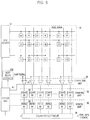
- FIG. 8 is a configuration diagram of an example of a CMOS image sensor implemented based on an embodiment of the disclosed technology.
- the CMOS image sensor based on an embodiment of the disclosed technology includes a pixel array 10 for outputting a pixel signal corresponding to incident light, a row decoder 20 , a ramp signal generator 830 , a comparison unit 40 , a counting unit 50 , a memory unit 60 , a control unit 80 , and a column readout circuit 70 .
- the row decoder 20 selects pixels in the pixel array 10 according to row lines and controls operations of the pixels under the control of the control unit 80 .
- the ramp signal generator 830 generates a ramp signal under the control of the control unit 80 .
- the comparison unit 40 compares a value of the ramp signal applied from the ramp signal generator 830 implemented based on various embodiments of the disclosed technology and the value of each pixel signal outputted from the pixel array 10 with each other according to instructions provided by the control unit 80 .
- the counting unit 50 counts clock signals of the control unit 80 according to each output signal of the comparison unit 40 .
- the memory unit 60 stores counting information of the counting unit 50 according to instructions provided by the control unit 80 .
- the control unit 80 controls the operations of the row decoder 20 , the ramp signal generator 830 implemented based on various embodiments of the disclosed technology, the comparison unit 40 , the counting unit 50 , the memory unit 60 , and the column readout circuit 70 .
- the column readout circuit 70 sequentially outputs data of the memory unit 60 as pixel data PXDATA according to instructions provided by the control unit 80 .
- the ramp signal generator 830 based on an embodiment of the disclosed technology may be implemented like the ramp signal generator described with reference to FIG. 3 , FIG. 4A to 4C , and FIG. 5 to FIG. 7 .
- a ramp signal generator includes a unit current cell including a current path that allows an electrical current constituting a ramp signal to flow from a ramp supply voltage terminal to a ramp resistor, and a slope control circuit coupled to the analog switch device and configured to receive a digital setting code value and generate a controllable analog reference voltage in response to the digital setting code to apply the controllable analog reference voltage to the analog switch device to control a slope of a ramp signal.
- the current path including an analog switch device coupled between the ramp supply voltage terminal and the ramp resistor.
- the unit current cell adjusts the slope of the ramp signal by adjusting a channel current flowing through the analog switch device based on the controllable analog reference voltage, which is adjustable in response to the digital setting code value.
- the slope control circuit includes a digital-to-analog converter (DAC) that converts the digital setting code value to the controllable analog reference voltage.
- DAC digital-to-analog converter
Landscapes
- Engineering & Computer Science (AREA)
- Multimedia (AREA)
- Signal Processing (AREA)
- Transforming Light Signals Into Electric Signals (AREA)
Abstract
Description
V RAMP =I TOTAL *R L (Equation 1)
V RAMP=(I TOTAL −I T_off)*R L (Equation 2)
ΔV=supply voltage−ground voltage (Equation 3)
ΔV=V CRV−ground voltage (Equation 4)
V RAMP=((I TM −I T-OFF)+(I T(N-M) −I RC))*R L (Equation 5)
Claims (17)
Applications Claiming Priority (2)
| Application Number | Priority Date | Filing Date | Title |
|---|---|---|---|
| KR1020180047291A KR102507628B1 (en) | 2018-04-24 | 2018-04-24 | Ramp Signal Generator, and CMOS Image Sensor Using That |
| KR10-2018-0047291 | 2018-04-24 |
Publications (2)
| Publication Number | Publication Date |
|---|---|
| US20190327438A1 US20190327438A1 (en) | 2019-10-24 |
| US11032505B2 true US11032505B2 (en) | 2021-06-08 |
Family
ID=68236613
Family Applications (1)
| Application Number | Title | Priority Date | Filing Date |
|---|---|---|---|
| US16/219,826 Active 2038-12-29 US11032505B2 (en) | 2018-04-24 | 2018-12-13 | Ramp signal generator and CMOS image sensor using the same |
Country Status (3)
| Country | Link |
|---|---|
| US (1) | US11032505B2 (en) |
| KR (1) | KR102507628B1 (en) |
| CN (1) | CN110401804B (en) |
Cited By (1)
| Publication number | Priority date | Publication date | Assignee | Title |
|---|---|---|---|---|
| US12439183B2 (en) * | 2022-10-25 | 2025-10-07 | Samsung Electronics Co., Ltd. | Ramp signal generator for calibrating ramp linearity, operating method thereof, and image sensor device including the same |
Families Citing this family (4)
| Publication number | Priority date | Publication date | Assignee | Title |
|---|---|---|---|---|
| KR20210141161A (en) | 2020-05-15 | 2021-11-23 | 에스케이하이닉스 주식회사 | Image sensing device and method of operating the same |
| CN113394239B (en) * | 2021-05-10 | 2023-08-18 | 汇顶科技私人有限公司 | Image sensor, fingerprint identification module and electronic device |
| CN115379143B (en) * | 2021-05-21 | 2025-03-11 | 格科微电子(上海)有限公司 | Image sensor ramp signal generation circuit and formation method |
| KR20230094514A (en) * | 2021-12-21 | 2023-06-28 | 에스케이하이닉스 주식회사 | Image sensor |
Citations (14)
| Publication number | Priority date | Publication date | Assignee | Title |
|---|---|---|---|---|
| KR20080034687A (en) | 2006-10-17 | 2008-04-22 | 삼성전자주식회사 | Lamp generator and its lamp signal generation method |
| US20080170137A1 (en) * | 2007-01-17 | 2008-07-17 | Sony Corporation | Solid-state imaging device and imaging apparatus |
| CN101227551A (en) | 2007-01-17 | 2008-07-23 | 索尼株式会社 | Solid-state imaging device and imaging device |
| US20090174442A1 (en) * | 2007-12-26 | 2009-07-09 | Soo Youn Kim | Ramp generator and image sensor including the same |
| US20100134083A1 (en) * | 2008-12-02 | 2010-06-03 | Olivier Trescases | System and method for a/d conversion |
| KR20120002274A (en) | 2010-06-30 | 2012-01-05 | 주식회사 하이닉스반도체 | Lamp Signal Generator and Image Sensor |
| US20120194367A1 (en) * | 2011-01-31 | 2012-08-02 | Hynix Semiconductor Inc. | Continuous ramp generator design and its calibration for cmos image sensors using single-ramp adcs |
| CN103002228A (en) | 2011-09-08 | 2013-03-27 | 佳能株式会社 | Solid-state imaging apparatus and method for driving solid-state imaging apparatus |
| US20150172580A1 (en) * | 2013-12-12 | 2015-06-18 | Cista System Corp. | Column comparator system and method for comparing a ramping signal and an input signal |
| US20160315602A1 (en) | 2015-04-24 | 2016-10-27 | SK Hynix Inc. | Ramp signal generator and cmos image sensor using the same |
| US20170127001A1 (en) * | 2015-10-28 | 2017-05-04 | SK Hynix Inc. | Ramp voltage generator, image sensing device including the same and method for driving the image sensing device |
| CN107070178A (en) | 2017-03-13 | 2017-08-18 | 黑龙江特通电气股份有限公司 | A kind of slope compensation circuit for automatically adjusting slope compensation slope |
| KR20190097704A (en) | 2018-02-13 | 2019-08-21 | 에스케이하이닉스 주식회사 | Comparator, and cmos image sensor thereof |
| US20200036924A1 (en) * | 2018-07-30 | 2020-01-30 | SK Hynix Inc. | Ramp signal generation device and cmos image sensor using the same |
Family Cites Families (3)
| Publication number | Priority date | Publication date | Assignee | Title |
|---|---|---|---|---|
| KR100790969B1 (en) * | 2005-08-23 | 2008-01-02 | 삼성전자주식회사 | Image Sensor and Method Using Automatically Corrected Lamp Signal for Image Quality Improvement |
| KR20100131729A (en) * | 2009-06-08 | 2010-12-16 | (주) 지안 | Lamp signal generator using a non-switching method and an image sensor including the same |
| KR102456577B1 (en) * | 2015-12-30 | 2022-10-20 | 에스케이하이닉스 주식회사 | Ramp Signal Generator, and CMOS Image Sensor Using That |
-
2018
- 2018-04-24 KR KR1020180047291A patent/KR102507628B1/en active Active
- 2018-12-03 CN CN201811465228.2A patent/CN110401804B/en active Active
- 2018-12-13 US US16/219,826 patent/US11032505B2/en active Active
Patent Citations (14)
| Publication number | Priority date | Publication date | Assignee | Title |
|---|---|---|---|---|
| KR20080034687A (en) | 2006-10-17 | 2008-04-22 | 삼성전자주식회사 | Lamp generator and its lamp signal generation method |
| US20080170137A1 (en) * | 2007-01-17 | 2008-07-17 | Sony Corporation | Solid-state imaging device and imaging apparatus |
| CN101227551A (en) | 2007-01-17 | 2008-07-23 | 索尼株式会社 | Solid-state imaging device and imaging device |
| US20090174442A1 (en) * | 2007-12-26 | 2009-07-09 | Soo Youn Kim | Ramp generator and image sensor including the same |
| US20100134083A1 (en) * | 2008-12-02 | 2010-06-03 | Olivier Trescases | System and method for a/d conversion |
| KR20120002274A (en) | 2010-06-30 | 2012-01-05 | 주식회사 하이닉스반도체 | Lamp Signal Generator and Image Sensor |
| US20120194367A1 (en) * | 2011-01-31 | 2012-08-02 | Hynix Semiconductor Inc. | Continuous ramp generator design and its calibration for cmos image sensors using single-ramp adcs |
| CN103002228A (en) | 2011-09-08 | 2013-03-27 | 佳能株式会社 | Solid-state imaging apparatus and method for driving solid-state imaging apparatus |
| US20150172580A1 (en) * | 2013-12-12 | 2015-06-18 | Cista System Corp. | Column comparator system and method for comparing a ramping signal and an input signal |
| US20160315602A1 (en) | 2015-04-24 | 2016-10-27 | SK Hynix Inc. | Ramp signal generator and cmos image sensor using the same |
| US20170127001A1 (en) * | 2015-10-28 | 2017-05-04 | SK Hynix Inc. | Ramp voltage generator, image sensing device including the same and method for driving the image sensing device |
| CN107070178A (en) | 2017-03-13 | 2017-08-18 | 黑龙江特通电气股份有限公司 | A kind of slope compensation circuit for automatically adjusting slope compensation slope |
| KR20190097704A (en) | 2018-02-13 | 2019-08-21 | 에스케이하이닉스 주식회사 | Comparator, and cmos image sensor thereof |
| US20200036924A1 (en) * | 2018-07-30 | 2020-01-30 | SK Hynix Inc. | Ramp signal generation device and cmos image sensor using the same |
Non-Patent Citations (1)
| Title |
|---|
| Office Action dated Apr. 6, 2021 in Chinese Patent Application No. 201811465228.2, 21 pages. |
Cited By (1)
| Publication number | Priority date | Publication date | Assignee | Title |
|---|---|---|---|---|
| US12439183B2 (en) * | 2022-10-25 | 2025-10-07 | Samsung Electronics Co., Ltd. | Ramp signal generator for calibrating ramp linearity, operating method thereof, and image sensor device including the same |
Also Published As
| Publication number | Publication date |
|---|---|
| CN110401804B (en) | 2022-02-01 |
| CN110401804A (en) | 2019-11-01 |
| KR20190123501A (en) | 2019-11-01 |
| US20190327438A1 (en) | 2019-10-24 |
| KR102507628B1 (en) | 2023-03-09 |
Similar Documents
| Publication | Publication Date | Title |
|---|---|---|
| US11032505B2 (en) | Ramp signal generator and CMOS image sensor using the same | |
| US11089253B2 (en) | Image sensor with controllable conversion gain | |
| US10819935B2 (en) | Ramp signal generator and CMOS image sensor using the same | |
| US10104326B2 (en) | Imaging apparatus including analog-to-digital conversion circuits to convert analog signals into digital signals, imaging system including analog-to-digital conversion circuits to convert analog signals into digital signals, and imaging apparatus driving method | |
| US8687098B2 (en) | Solid-state imaging device, control method therefor, and camera system | |
| US8421889B2 (en) | Image pickup apparatus, image pickup system, and method of the image pickup apparatus having pixel array for outputting an analog signal | |
| US7245321B2 (en) | Readout circuit with gain and analog-to-digital conversion for image sensor | |
| JP5165520B2 (en) | Solid-state imaging device, imaging device, and AD conversion method for solid-state imaging device | |
| US20060284999A1 (en) | Solid-state imaging device, analogue-digital converting method in solid-state imaging device and imaging apparatus | |
| US11284032B2 (en) | Imaging device, semiconductor device and camera | |
| US10721427B2 (en) | Image sensor circuit and ramp signal generator thereof | |
| US10142559B2 (en) | Pixel signal transfer device and method thereof and CMOS image sensor including the same | |
| JP2006018663A (en) | Current stabilization circuit, current stabilization method, and solid-state imaging device | |
| US10958858B2 (en) | Ramp signal generator and image sensor including the same | |
| US11336845B2 (en) | Image sensor and driving method thereof | |
| US7242332B1 (en) | Column-parallel sigma-delta analog-to-digital conversion with gain and offset control | |
| US10757356B2 (en) | Comparison device and CMOS image sensor including the same | |
| JP2011259485A (en) | Solid-state imaging device, imaging apparatus, and ad conversion gain adjusting method | |
| US10805568B2 (en) | Ramp signal generation device and CMOS image sensor using the same | |
| US10931268B2 (en) | Ramp signal generation device and CMOS image sensor including the same | |
| US20250119668A1 (en) | Ramp signal generator and image sensor and electronic device including the same |
Legal Events
| Date | Code | Title | Description |
|---|---|---|---|
| AS | Assignment |
Owner name: SK HYNIX INC., KOREA, REPUBLIC OF Free format text: ASSIGNMENT OF ASSIGNORS INTEREST;ASSIGNORS:KIM, HYEON-JUNE;JEONG, HOE-SAM;REEL/FRAME:047772/0818 Effective date: 20181024 |
|
| FEPP | Fee payment procedure |
Free format text: ENTITY STATUS SET TO UNDISCOUNTED (ORIGINAL EVENT CODE: BIG.); ENTITY STATUS OF PATENT OWNER: LARGE ENTITY |
|
| STPP | Information on status: patent application and granting procedure in general |
Free format text: NON FINAL ACTION MAILED |
|
| STPP | Information on status: patent application and granting procedure in general |
Free format text: RESPONSE TO NON-FINAL OFFICE ACTION ENTERED AND FORWARDED TO EXAMINER |
|
| STPP | Information on status: patent application and granting procedure in general |
Free format text: NOTICE OF ALLOWANCE MAILED -- APPLICATION RECEIVED IN OFFICE OF PUBLICATIONS |
|
| STPP | Information on status: patent application and granting procedure in general |
Free format text: PUBLICATIONS -- ISSUE FEE PAYMENT RECEIVED |
|
| STPP | Information on status: patent application and granting procedure in general |
Free format text: PUBLICATIONS -- ISSUE FEE PAYMENT VERIFIED Free format text: AWAITING TC RESP, ISSUE FEE PAYMENT VERIFIED |
|
| STPP | Information on status: patent application and granting procedure in general |
Free format text: PUBLICATIONS -- ISSUE FEE PAYMENT VERIFIED |
|
| STCF | Information on status: patent grant |
Free format text: PATENTED CASE |
|
| MAFP | Maintenance fee payment |
Free format text: PAYMENT OF MAINTENANCE FEE, 4TH YEAR, LARGE ENTITY (ORIGINAL EVENT CODE: M1551); ENTITY STATUS OF PATENT OWNER: LARGE ENTITY Year of fee payment: 4 |