US11031492B2 - Semiconductor structure comprising III-N material - Google Patents
Semiconductor structure comprising III-N material Download PDFInfo
- Publication number
- US11031492B2 US11031492B2 US16/091,478 US201716091478A US11031492B2 US 11031492 B2 US11031492 B2 US 11031492B2 US 201716091478 A US201716091478 A US 201716091478A US 11031492 B2 US11031492 B2 US 11031492B2
- Authority
- US
- United States
- Prior art keywords
- layer
- section
- semiconductor structure
- interlayer
- superlattice
- Prior art date
- Legal status (The legal status is an assumption and is not a legal conclusion. Google has not performed a legal analysis and makes no representation as to the accuracy of the status listed.)
- Active, expires
Links
Images


Classifications
-
- H—ELECTRICITY
- H10—SEMICONDUCTOR DEVICES; ELECTRIC SOLID-STATE DEVICES NOT OTHERWISE PROVIDED FOR
- H10D—INORGANIC ELECTRIC SEMICONDUCTOR DEVICES
- H10D30/00—Field-effect transistors [FET]
- H10D30/40—FETs having zero-dimensional [0D], one-dimensional [1D] or two-dimensional [2D] charge carrier gas channels
- H10D30/47—FETs having zero-dimensional [0D], one-dimensional [1D] or two-dimensional [2D] charge carrier gas channels having two-dimensional [2D] charge carrier gas channels, e.g. nanoribbon FETs or high electron mobility transistors [HEMT]
- H10D30/471—High electron mobility transistors [HEMT] or high hole mobility transistors [HHMT]
- H10D30/473—High electron mobility transistors [HEMT] or high hole mobility transistors [HHMT] having confinement of carriers by multiple heterojunctions, e.g. quantum well HEMT
- H10D30/4732—High electron mobility transistors [HEMT] or high hole mobility transistors [HHMT] having confinement of carriers by multiple heterojunctions, e.g. quantum well HEMT using Group III-V semiconductor material
-
- H01L29/7783—
-
- H—ELECTRICITY
- H10—SEMICONDUCTOR DEVICES; ELECTRIC SOLID-STATE DEVICES NOT OTHERWISE PROVIDED FOR
- H10D—INORGANIC ELECTRIC SEMICONDUCTOR DEVICES
- H10D30/00—Field-effect transistors [FET]
- H10D30/40—FETs having zero-dimensional [0D], one-dimensional [1D] or two-dimensional [2D] charge carrier gas channels
- H10D30/47—FETs having zero-dimensional [0D], one-dimensional [1D] or two-dimensional [2D] charge carrier gas channels having two-dimensional [2D] charge carrier gas channels, e.g. nanoribbon FETs or high electron mobility transistors [HEMT]
-
- H—ELECTRICITY
- H10—SEMICONDUCTOR DEVICES; ELECTRIC SOLID-STATE DEVICES NOT OTHERWISE PROVIDED FOR
- H10P—GENERIC PROCESSES OR APPARATUS FOR THE MANUFACTURE OR TREATMENT OF DEVICES COVERED BY CLASS H10
- H10P14/00—Formation of materials, e.g. in the shape of layers or pillars
- H10P14/20—Formation of materials, e.g. in the shape of layers or pillars of semiconductor materials
- H10P14/29—Formation of materials, e.g. in the shape of layers or pillars of semiconductor materials characterised by the substrates
- H10P14/2901—Materials
- H10P14/2902—Materials being Group IVA materials
- H10P14/2905—Silicon, silicon germanium or germanium
-
- H01L21/02455—
-
- H01L29/15—
-
- H01L29/66462—
-
- H—ELECTRICITY
- H10—SEMICONDUCTOR DEVICES; ELECTRIC SOLID-STATE DEVICES NOT OTHERWISE PROVIDED FOR
- H10D—INORGANIC ELECTRIC SEMICONDUCTOR DEVICES
- H10D30/00—Field-effect transistors [FET]
- H10D30/01—Manufacture or treatment
- H10D30/015—Manufacture or treatment of FETs having heterojunction interface channels or heterojunction gate electrodes, e.g. HEMT
-
- H—ELECTRICITY
- H10—SEMICONDUCTOR DEVICES; ELECTRIC SOLID-STATE DEVICES NOT OTHERWISE PROVIDED FOR
- H10D—INORGANIC ELECTRIC SEMICONDUCTOR DEVICES
- H10D62/00—Semiconductor bodies, or regions thereof, of devices having potential barriers
- H10D62/80—Semiconductor bodies, or regions thereof, of devices having potential barriers characterised by the materials
- H10D62/81—Semiconductor bodies, or regions thereof, of devices having potential barriers characterised by the materials of structures exhibiting quantum-confinement effects, e.g. single quantum wells; of structures having periodic or quasi-periodic potential variation
- H10D62/815—Semiconductor bodies, or regions thereof, of devices having potential barriers characterised by the materials of structures exhibiting quantum-confinement effects, e.g. single quantum wells; of structures having periodic or quasi-periodic potential variation of structures having periodic or quasi-periodic potential variation, e.g. superlattices or multiple quantum wells [MQW]
-
- H—ELECTRICITY
- H10—SEMICONDUCTOR DEVICES; ELECTRIC SOLID-STATE DEVICES NOT OTHERWISE PROVIDED FOR
- H10P—GENERIC PROCESSES OR APPARATUS FOR THE MANUFACTURE OR TREATMENT OF DEVICES COVERED BY CLASS H10
- H10P14/00—Formation of materials, e.g. in the shape of layers or pillars
- H10P14/20—Formation of materials, e.g. in the shape of layers or pillars of semiconductor materials
- H10P14/24—Formation of materials, e.g. in the shape of layers or pillars of semiconductor materials using chemical vapour deposition [CVD]
-
- H—ELECTRICITY
- H10—SEMICONDUCTOR DEVICES; ELECTRIC SOLID-STATE DEVICES NOT OTHERWISE PROVIDED FOR
- H10P—GENERIC PROCESSES OR APPARATUS FOR THE MANUFACTURE OR TREATMENT OF DEVICES COVERED BY CLASS H10
- H10P14/00—Formation of materials, e.g. in the shape of layers or pillars
- H10P14/20—Formation of materials, e.g. in the shape of layers or pillars of semiconductor materials
- H10P14/29—Formation of materials, e.g. in the shape of layers or pillars of semiconductor materials characterised by the substrates
- H10P14/2926—Crystal orientations
-
- H—ELECTRICITY
- H10—SEMICONDUCTOR DEVICES; ELECTRIC SOLID-STATE DEVICES NOT OTHERWISE PROVIDED FOR
- H10P—GENERIC PROCESSES OR APPARATUS FOR THE MANUFACTURE OR TREATMENT OF DEVICES COVERED BY CLASS H10
- H10P14/00—Formation of materials, e.g. in the shape of layers or pillars
- H10P14/20—Formation of materials, e.g. in the shape of layers or pillars of semiconductor materials
- H10P14/32—Formation of materials, e.g. in the shape of layers or pillars of semiconductor materials characterised by intermediate layers between substrates and deposited layers
- H10P14/3202—Materials thereof
- H10P14/3214—Materials thereof being Group IIIA-VA semiconductors
- H10P14/3216—Nitrides
-
- H—ELECTRICITY
- H10—SEMICONDUCTOR DEVICES; ELECTRIC SOLID-STATE DEVICES NOT OTHERWISE PROVIDED FOR
- H10P—GENERIC PROCESSES OR APPARATUS FOR THE MANUFACTURE OR TREATMENT OF DEVICES COVERED BY CLASS H10
- H10P14/00—Formation of materials, e.g. in the shape of layers or pillars
- H10P14/20—Formation of materials, e.g. in the shape of layers or pillars of semiconductor materials
- H10P14/32—Formation of materials, e.g. in the shape of layers or pillars of semiconductor materials characterised by intermediate layers between substrates and deposited layers
- H10P14/3242—Structure
- H10P14/3244—Layer structure
- H10P14/3251—Layer structure consisting of three or more layers
- H10P14/3252—Alternating layers, e.g. superlattice
-
- H—ELECTRICITY
- H10—SEMICONDUCTOR DEVICES; ELECTRIC SOLID-STATE DEVICES NOT OTHERWISE PROVIDED FOR
- H10P—GENERIC PROCESSES OR APPARATUS FOR THE MANUFACTURE OR TREATMENT OF DEVICES COVERED BY CLASS H10
- H10P14/00—Formation of materials, e.g. in the shape of layers or pillars
- H10P14/20—Formation of materials, e.g. in the shape of layers or pillars of semiconductor materials
- H10P14/34—Deposited materials, e.g. layers
- H10P14/3402—Deposited materials, e.g. layers characterised by the chemical composition
- H10P14/3414—Deposited materials, e.g. layers characterised by the chemical composition being group IIIA-VIA materials
- H10P14/3416—Nitrides
-
- H—ELECTRICITY
- H10—SEMICONDUCTOR DEVICES; ELECTRIC SOLID-STATE DEVICES NOT OTHERWISE PROVIDED FOR
- H10P—GENERIC PROCESSES OR APPARATUS FOR THE MANUFACTURE OR TREATMENT OF DEVICES COVERED BY CLASS H10
- H10P14/00—Formation of materials, e.g. in the shape of layers or pillars
- H10P14/20—Formation of materials, e.g. in the shape of layers or pillars of semiconductor materials
- H10P14/34—Deposited materials, e.g. layers
- H10P14/3438—Doping during depositing
- H10P14/3441—Conductivity type
- H10P14/3444—P-type
-
- H—ELECTRICITY
- H10—SEMICONDUCTOR DEVICES; ELECTRIC SOLID-STATE DEVICES NOT OTHERWISE PROVIDED FOR
- H10P—GENERIC PROCESSES OR APPARATUS FOR THE MANUFACTURE OR TREATMENT OF DEVICES COVERED BY CLASS H10
- H10P14/00—Formation of materials, e.g. in the shape of layers or pillars
- H10P14/20—Formation of materials, e.g. in the shape of layers or pillars of semiconductor materials
- H10P14/34—Deposited materials, e.g. layers
- H10P14/3438—Doping during depositing
- H10P14/3441—Conductivity type
- H10P14/3446—Transition metal elements; Rare earth elements
Definitions
- This disclosure relates to a semiconductor structure comprising III-N materials.
- III-N materials are particularly useful for receiving transistors of the HEMT (High Electron Mobility Transistor) type that spin off, for instance, as a switch in power converters.
- HEMT High Electron Mobility Transistor
- the electrically conducting state of the transistor between the source S and drain D is controlled by the voltage applied to the gate G.
- the transistor when the voltage applied to the gate G exceeds a threshold voltage Vt, the transistor is on.
- Vt a threshold voltage
- the voltage V DS that develops in this case between the two electrodes ranges from a few volts to a few dozen volts, and is related to the resistivity of the channel layer material.
- the transistor When the voltage applied to the gate G is lower than the threshold voltage Vt, the transistor is off. In the case of power application, the voltage V DS that applies across the terminals of the source S and drain D electrodes can then range from a few hundred volts to a few thousand volts. The leakage current flowing between the source S and the drain D is low, up to a few nanoamperes per mm of gate width.
- the transistor By controlling the gate voltage, the transistor can be switched very rapidly (within nanoseconds) between an on state and an off state.
- a high voltage is applied across the terminals of the source S and drain D electrodes. This leads to the formation of an electric field whose lines penetrate very deep into the main layer 3 and the substrate 2 .
- An electric field which may be of high intensity, then develops between the drain electrode D and the substrate 2 , particularly in the thickness of the main layer 3 , and between the source S and drain D.
- the breakdown field the critical value at which the material can no longer support it.
- provision must be made to separate the drain D and the source S by a sufficient distance d such that for a given voltage V DS , the field strength E V DS /d is less than the breakdown field.
- a main layer 3 must be provided with sufficient thickness such that the voltage that develops between the substrate 2 and the drain D (which may be up to V DS ) leads to a field strength that is also lower in the materials involved than the breakdown field.
- Providing a semiconductor structure 1 having a main layer 3 of sufficiently thick III-N materials (about 3 microns or more) is, however, much more difficult, especially when the selected substrate 2 is made of silicon rather than sapphire because of availability and cost.
- documents EP1290721 and WO 2013/001014 provide examples of known techniques for growing a thick main layer 3 of a III-N material on a support substrate 2 , which may be made of silicon. These techniques include inserting into the buffer layer made of III-N materials at least one interlayer, also made of III-N material, whose nature is chosen in order to compress a portion of the buffer layer with which it comes into contact.
- Another problem that limits the spread of the technology concerns the leakage current flowing in the thickness of the main layer 3 between the source S and the drain D when the transistor is in the off state. Of course, it is hoped that this current be as little as possible. That is why the main layer 3 is generally doped with a p-type doping agent, such as iron, carbon or magnesium, to make it resistive and limit in such manner the flow of leakage currents.
- a p-type doping agent such as iron, carbon or magnesium
- the semiconductor structure 1 may have an excessive leakage current for the intended applications.
- the present disclosure aims to overcome all or part of the aforementioned drawbacks. It particularly aims at providing a semiconductor structure having, on a support substrate, a thick main layer that is highly resistive in order to form a transistor that can withstand high voltages, and limiting the intensity of leakage currents.
- the purpose of the disclosure is to provide a semiconductor structure comprising III-N materials made up of:
- the interlayer thus formed is particularly effective in limiting the leakage current or the density of leakage current in the structure.
- the disclosure also relates to a semiconductor silicon wafer or an integrated circuit device comprising a semiconductor structure as shown.
- the formation of the interlayer comprises:
- the first temperature is lower than the second temperature.
- FIG. 1 shows a prior art semiconductor structure having a HEMT
- FIG. 2 shows a semiconductor structure comprising III-N materials according to the present disclosure
- FIG. 3 shows another semiconductor structure comprising III-N materials according to the present disclosure
- FIG. 4 graphically illustrates the leakage current performance of a semiconductor structure according to the present disclosure.
- FIG. 2 shows a semiconductor structure comprising III-N materials according to the present disclosure.
- the semiconductor structure 1 may take the form of a standard size, circular semiconductor wafer, for example, 150 mm, 200 mm or even 300 mm, but the disclosure is not limited to this shape or these dimensions. Thus, where and when the semiconductor structure 1 forms part of a singled out, finished or semi-finished, integrated circuit device, it will either take the shape of a rectangular or square block of material, measuring just a few millimeters to a few centimeters, with the dimensions of the integrated circuit device.
- the semiconductor structure 1 comprises a support substrate 2 capable of receiving a crystalline layer epitaxially made of III-N material.
- the support substrate 2 is advantageously made of monocrystalline silicon, preferably crystalline orientation (111), but the disclosure is not limited to this material and this orientation.
- it may be made of silicon carbide, massive gallium nitride, silicon (110) or (001) or an advanced substrate such as silicon-on-insulator or silicon carbide-on-insulator.
- the main layer 3 comprises a first section 3 a provided on the support substrate 2 and a second section 3 b disposed on the first section 3 a.
- each section 3 a , 3 b may have different compositions from each other.
- each section 3 a , 3 b may also be made up of a plurality of different sub-layers of composition or nature from each other.
- the main layer 3 provides a material thickness that makes it possible to separate an integrated circuit device formed on the semiconductor structure 1 from the support substrate 2 . This limits the intensity of the electric field that develops between the support substrate 2 and the source S or drain D electrode, for a given voltage when the device is “on.”
- the thickness of the main layer 3 (that is to say, the thickness of material between the upper face of the support substrate 2 and the free face of the semiconductor structure 1 ) is greater than 3 microns, or 5 microns or 10 microns. A considerable thickness makes it possible to form an integrated circuit device on the semiconductor structure 1 that can be subjected to a high voltage without breaking down (more than 1000 V, for example).
- the main layer 3 is doped to make it resistive.
- this may be a carbon doping whose concentration in the main layer may be between 5 ⁇ 10 18 and 5 ⁇ 10′ 19 at/cm 3 . It can also be of another p-type doping agent, for example, iron or magnesium.
- This concentration is not necessarily uniform in the main layer 3 and in the sections 3 a , 3 b of the main layer 3 . It can vary within this layer and/or the sections 3 a , 3 b , particularly in a perpendicular direction to the support substrate 2 .
- the first section 3 a of the main layer 3 which is in contact with the support substrate 2 , may comprise a first nucleation sublayer, in contact with the support substrate 2 , of a few hundred nm thick, for example, made of AlN (not shown in FIG. 2 ), facilitating the epitaxy of the rest of the main layer 3 on the support substrate 2 .
- This nucleation sublayer made of AlN is particularly useful when the support substrate 2 is made of silicon.
- the first section 3 a may also comprise one or more other sub-layers, for example, GaN or AlGaN, a homogeneous composition or as superlattice (these terms will be defined later).
- the difference in coefficients of thermal expansion that may exist between the support substrate 2 and the monocrystalline main layer 3 can lead to the generation of high stress in these elements during high-temperature formation of the main layer 3 and/or after its formation, especially when cooling the structure.
- the support substrate 2 has a coefficient of thermal expansion that is less than that of the main layer 3
- this layer after its high-temperature formation and return to ambient temperature, is subjected to tensile stress that can lead to its stress cracking. This is particularly the case when the main layer 3 has a thickness greater than a few microns.
- the disclosure provides an interlayer 4 made of monocrystalline III-N material interposed in the main layer 3 and disposed between the first section 3 a and the second section 3 b .
- This interlayer 4 is configured in order to compress the second section 3 b of the main layer 3 , during its high-temperature epitaxial formation. During the return to ambient temperature, this compression offsets the tensile stresses that can lead to its cracking when the support substrate 2 has a lower coefficient of thermal expansion than the main layer 3 .
- the interlayer 4 is composed of a lower layer 4 a disposed on the first section 3 a of the main layer 3 and an upper layer 4 b disposed on and in contact with, the lower layer 4 a.
- the nature and composition of the interlayer 4 are chosen so that the lattice parameter of the material forming the lower layer 4 a is smaller than the lattice parameter of the material forming the upper layer 4 b .
- the former is preferred for being smaller than the lattice parameter of the material forming the second section 3 b .
- the upper layer 4 b is directly in contact with the lower layer 4 a .
- the term “lattice parameter of a layer of material” refers to the lattice parameter of the material in the plane defined by the layer.
- the lower layer 4 a may have a uniform composition. Alternatively, it may be formed by a superlattice. In both cases, the main function of the lower layer 4 a is to compress the second section 3 b of the main layer 3 . To facilitate this compression, and as recalled in document US2006/0191474 mentioned in the background of the disclosure, the lower layer 4 a is formed at a first relatively low temperature, for example, below 1000° C. In consequence thereof, it has a lower crystalline quality and, more particularly, has a concentration of threading dislocations that can reach 10 10 or 10 11 per cm 2 , as may be determined by a TEM or SEM analysis. This concentration is much greater than the concentration dislocations present in the layers obtained at a second more conventional temperature of over 1000° C. and typically between 1050° C. and 1100° C. during the MOCVD formation of layers made of III-N materials. These dislocations form preferred passages for current and, therefore, lead to decreasing the electrical resistivity of the structure.
- a first relatively low temperature for
- the interlayer 4 also comprises an upper layer 4 b formed by a superlattice.
- the upper layer 4 b is formed at a second conventional temperature above the first temperature. It may be well above 1000° C., and typically between 1050° C. and 1100° C.
- the upper layer 4 b has a dislocation density lower than that of the lower layer 4 a .
- the upper layer 4 b is particularly effective for improving the electrical properties of the stack and offsetting electrical faults of the lower layer 4 a on which it rests.
- superlattice and according to the usual definition in the field of semiconductors, means a periodic stack of thin layers, for example, between 0.5 nm and 20 nm or even 50 nm. As this is well known per se, a superlattice layer formed is macroscopically similar to a uniform composition layer, as can be visible by photoluminescence or cathodoluminescence diffraction ray analysis. It should be specified that the lattice parameter of a superlattice layer corresponds to the lattice parameter of the equivalent uniform layer (whose composition can be visible by photoluminescence or cathodoluminescence X-ray diffraction).
- the lower and/or upper layers 4 a , 4 b are advantageously doped (p-type) to make them resistive. It may be a carbon, iron or magnesium doping in a concentration, which may range from 5 ⁇ 10 18 to 5 ⁇ 10 19 at/cm 3 .
- the interlayer 4 has a thickness that may be between 10 nm and 1000 nm or between 200 nm and 1000 nm in order to maintain the effective compression of parts of the second section 3 b of the main layer 3 , without requiring any excessive thickness.
- each of the upper and lower layers 4 b , 4 a may have a thickness of between 10 nm and about 1000 nm.
- both the lower layer 4 a and the upper layer 4 b are superlattices, they have different densities of threading dislocations, such that it is possible to distinguish two distinct layers from each other in the stack.
- Forming the upper layer 4 b shaped as a superlattice rather than as a uniform layer has many advantages.
- this layer e.g., with carbon and in the above-mentioned concentration range of 5 ⁇ 10 18 to 5 ⁇ 10 19 at/cm 3 ) without damaging the crystalline quality of these layers.
- a high concentration of doping agent in a uniform layer of III-N material can result in the formation of holes or other surface morphological defects. These defects result in making the semiconductor structure that contains them unfit to receive an integrated circuit device, particularly a high-performance, power device. They lead to high leakage currents and reduced breakdown voltage.
- the upper layer 4 b embodied as a superlattice prevents the appearance of these defects, even when these layers are doped at high concentration.
- at least this layer is doped at high concentration (for example, with carbon and in the above concentration range from 5 ⁇ 10 18 to 5 ⁇ 10 19 at/cm 3 ). Provision can then be made for an interlayer 4 and a highly resistive semiconductor structure 1 that limit the leakage currents of an integrated circuit device formed on such a semiconductor structure 1 .
- many interfaces that make up the stack of layers forming the superlattice appear beneficial for insulating and limiting leakage currents of the semiconductor structure 1 .
- they prevent or limit the occurrence of a conductive electronic plane (which enhances the flow of leakage currents) under the upper layer 4 b (and beneath the lower layer 4 a when the latter is formed from a superlattice), which sometimes occurs when the interlayer 4 consists of a uniform layer (forming a heterojunction with the underlying layer) of the background of the disclosure.
- the superlattice upper layer 4 b forms an effective barrier for free carriers of the semiconductor structure 1 .
- the superlattice forming the upper layer 4 b and, if necessary, the lower layer 4 a can be formed of a pattern repetition, the pattern comprising at least two layers.
- the natures of the two layers are different, that is to say, at least two of the pairs (w1, w2), (x1, x2), (y1, y2), (z1, z2) are different.
- Each layer that forms the pattern is very thin, typically between 0.5 nm and 20 nm, or even 50 nm.
- layer thicknesses should be chosen so as to be less than their critical thicknesses and limit the formation of dislocations. But the disclosure is not limited to this superlattice shape, and may provide a degree of relaxation in layers. Furthermore, the layer thicknesses of the pattern may be mutually identical or different.
- the pattern constituting the upper layer 4 b may be repeated from 2 to 500 times, depending on the respective layer thicknesses that it comprises, so as to form an upper layer 4 b having a thickness of between 10 nanometers and about 1000 nanometers.
- the interlayer 4 is preferably centrally placed within the thickness of the main layer 3 , that is to say, the thicknesses of the first section 3 a and the second section 3 b may be substantially identical (close to 50%). Stresses that develop in the material can be efficiently controlled during manufacture.
- the semiconductor structure 1 may have more than one interlayer, particularly when the thickness of the main layer 3 is significant, especially more than 5 microns.
- FIG. 3 shows a semiconductor structure 1 ′ comprising a semiconductor structure 1 similar in all respects to that shown in FIG. 2 , which has been described in detail.
- a second monocrystalline interlayer 4 c has been formed, on which is disposed a third section 3 c of the monocrystalline main layer 3 .
- the second interlayer 4 c compresses the third section 3 c of the main layer 3 .
- the material that the second interlayer 4 c is composed of has a lower lattice parameter than the material that makes up the third section 3 c of the main layer 3 .
- the second interlayer 4 c may take any suitable shape: it may be composed or comprised of a uniform layer, a superlattice, or a combination thereof. It may, in particular, be composed of a lower layer and an upper layer similar to what has been described in connection with interlayer 4 .
- a structure composed of a second interlayer 4 c and of a third section 3 c may be stacked as many times as necessary on the semiconductor structure 1 in order to form a main layer 3 of substantial thickness and satisfactory crystalline quality.
- the semiconductor structure 1 , 1 ′ of the present disclosure is achieved by growth, for example, by vapor phase epitaxy (“Metal Organic Chemical Vapor Deposition”) or “Molecular Beam Epitaxy.”
- the support substrate 2 (or a plurality of support substrates) is placed in a deposition chamber of conventional equipment.
- the support substrate 2 may be prepared prior to deposition so as to remove a native oxide layer from its surface.
- the chamber is crossed by precursor and carrier gas flows, at high temperatures typically between 1050° C. and 1150° C. for most of the layers that form the structure, and kept at a pressure of about 100 mbar, and typically between 50 mbar and 200 mbar.
- the growth conditions, i.e., temperature, pressure, gas flows are used to select the composition, quality and thickness of each stacking element forming the semiconductor structure 1 , 1 ′.
- the lower layer 4 a is formed at a first relatively low temperature, below the formation temperature of the upper layer 4 b , in order to facilitate the stressing of the second section 3 b of the main layer 3 .
- the precursor gas of the element Ga may be tri-methyl gallium (composition Ga(CH 3 ) 3 ) or tri-ethylgallium (composition Ga(C 2 H 5 ) 3 )
- the precursor gas of the element Al may be tri-methyl aluminum (composition Al 2 (CH 3 ) 6 ) or tri-ethyl aluminum (composition Al 2 (C 2 H 5 ) 6 )
- the precursor of element III may be ammonia (NH 3 ); and the carrier gas may comprise or consist of hydrogen and/or nitrogen.
- the growing conditions also help control the proportion of carbon that is incorporated into the layers during the growing in order to dope them intrinsically.
- an additional p-type extrinsic doping source may be used to make some layers resistive. This may be an iron, a carbon or a magnesium doping source.
- the extrinsic doping source may be CCl 4 , CBr 4 , C 2 H 2 , C 2 H 4 , C 6 H 12 , etc.
- a wafer of 200 mm silicon 111 is placed in a deposition chamber of an AIXTRON® or a VEECO®-type MOCVD reactor.
- An AlN nucleation layer of 100 nm to 300 nm thick is first formed on this wafer.
- a main layer 3 of GaN 5 microns thick is formed on the nucleation layer.
- an interlayer 4 has been formed.
- This interlayer is composed of a lower layer 4 a of uniform AlN composition with a thickness of 17 nm. This layer has a dislocation density above 10 10 /cm 2 .
- a superlattice upper layer 4 b is formed consisting of 100 repetitions of a pattern formed from a first layer of AlGaN having a 20% Al concentration and a thickness of 1 nm, and a second GaN layer having a thickness of 1 nm.
- This layer has a dislocation density below 10 10 /cm 2 .
- the interlayer 4 thus has a 217 nm thickness and the superlattice upper layer 4 b is macroscopically similar to a homogeneous AlGaN layer whose aluminum content is 10%.
- the AlN layer forming the lower layer and, to a certain extent, the superlattice forming the upper layer 4 b have a smaller lattice parameter than that of the GaN constituting the main layer 3 , and which enables the section of this main layer 3 to remain compressed.
- the main layer 3 and the interlayers 4 a , 4 b are all doped with carbon at a concentration of about 10 19 at/cm 3 during their growth.
- the main layer 3 of GaN has satisfactory crystalline quality and has no particular cracking, which would make it unfit for receiving an integrated circuit device.
- the interlayer comprises a lower superlattice layer 4 a .
- the lower layer 4 a is composed of 10 repetitions of a pattern formed by a first AlN layer having a thickness of 1 nm and a second GaN layer having a thickness of 0.5 nm.
- the lower superlattice layer 4 a is macroscopically similar to a homogeneous AlGaN layer having a thickness of 15 nm and an aluminum content of 66%.
- This example relates to a semiconductor structure having two interlayers.
- a second interlayer consisting of a uniform layer of AlGaN having a concentration of 80% aluminum and a thickness of 20 nm is formed on the semiconductor structure of Example 1.
- a third GaN section having a thickness of 1 micron is formed on the AlGaN layer.
- the second interlayer consists of a superlattice.
- the superlattice is formed from five repetitions of a pattern formed from an AlN layer having a thickness of 2 nm and a layer of AlGaN (60% Al) having a thickness of 2 nm.
- Example 1 This counter-example is similar to the structure of Example 1 wherein the upper superlattice layer 4 b has been replaced by a uniform upper layer of AlGaN (10% aluminum content) having a thickness of 200 nm.
- the only difference between the semiconductor structure of Example 1 and Counter-Example 1 is that in Example 1, the upper layer is made in the form of a superlattice while in Counter-Example 1, the upper layer is made in the form of a homogeneous layer.
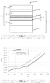
- FIG. 4 graphically illustrates efficiency in density of leakage current of the structure in Example 1 and the structure in Counter-Example 1.
- the x-axis represents a vertical voltage (expressed in volts) applied on both sides of the structure, i.e., between the free face of the support substrate 2 , on the one hand, and the free face of the main layer 3 , on the other hand.
- the y-axis represents the current density flowing between these two surfaces (expressed in Amperes/mm 2 and on a logarithmic scale).
- the density of leakage current in the case of the semiconductor structure in Example 1 is shown in this graph by the solid line.
- the density of leakage current in the case of the semiconductor structure in Counter-Example 1 is shown in this graph by the dotted line. The measurements were performed at ambient temperature.
- Example 1 saves about one order of current density, regardless of the voltage applied to at least 1000 volts. It is, therefore, understood that an integrated circuit device (such as an HEMT device) having a defined geometry formed on the structure of Example 1 has a leakage current of about ten times less than the same device, also having the same geometry, but formed on the structure of Counter-Example 1.
- an integrated circuit device such as an HEMT device
- semiconductor structure 1 in a power application has been shown when it is equipped with an integrated HEMT-type device, the disclosure is not limited to this application or to this type of device.
- the semiconductor structure 1 of the present disclosure will, therefore, be beneficial in the field of radio frequencies, light-emitting diodes and any other application or device for which the electrical properties described are advantageous.
Landscapes
- Junction Field-Effect Transistors (AREA)
- Chemical & Material Sciences (AREA)
- Crystallography & Structural Chemistry (AREA)
- Crystals, And After-Treatments Of Crystals (AREA)
- Chemical Vapour Deposition (AREA)
- Inorganic Chemistry (AREA)
- Engineering & Computer Science (AREA)
- Materials Engineering (AREA)
Abstract
Description
-
- a
sapphire substrate 2 and amain layer 3 of A1N forming thesemiconductor structure 1; - a heterojunction consisting of a
GaN channel layer 5 and anAlGaN barrier layer 6 successively formed on the semiconductor structure; - source S, drain D and gate G electrodes on/in the heterojunction.
- a
-
- a support substrate;
- a main layer made of III-N material, the main layer having a first section disposed on the support substrate and a second section disposed on the first section;
- an interlayer of III-N material disposed between the first section and the second section in order to compress the second section of the main layer,
- wherein, the interlayer comprises:
- a lower layer disposed on the first section of the main layer;
- an upper layer disposed on and in contact with the lower layer formed by a superlattice, and
- wherein, the lower layer has a higher dislocation density than the upper layer.
-
- the lower layer consists of a superlattice, different from the superlattice forming the upper layer, or of a homogeneous layer;
- the lattice parameter of the material that forms the lower layer is smaller than the lattice parameter of the material forming the upper layer;
- the lattice parameter of the material that forms the upper layer is smaller than the lattice parameter of the material forming the lower layer;
- the main layer and the interlayer are monocrystalline;
- the semiconductor structure comprises a second interlayer on the second section of the main layer and a third section of the main layer disposed on the second interlayer;
- the second interlayer consists of a homogeneous layer, a superlattice, or a combination thereof;
- at least the upper layer comprises a p-type doping agent;
- the support substrate has a lower coefficient of thermal expansion than that of the main layer.
-
- the formation of a main layer made of III-N material on the carrier substrate, the main layer having a first section and a second section disposed on the first section;
- the formation of an interlayer made of III-N material disposed between the first section and the second section in order to compress the second section of the main layer.
-
- the formation, at a first temperature, of a lower layer disposed on the first section of the main layer;
- and the formation, at a second temperature, of an upper layer formed by a superlattice and disposed on and in contact with the lower layer.
-
- the first temperature is lower than 1000° C.;
- the second temperature ranges between 1050° C. and 1100° C.
Claims (8)
Applications Claiming Priority (3)
| Application Number | Priority Date | Filing Date | Title |
|---|---|---|---|
| FR1652983A FR3049762B1 (en) | 2016-04-05 | 2016-04-05 | SEMICONDUCTOR STRUCTURE BASED ON III-N MATERIAL |
| FR1652983 | 2016-04-05 | ||
| PCT/FR2017/050467 WO2017174885A1 (en) | 2016-04-05 | 2017-03-01 | Semiconductor structure comprising iii-n material |
Publications (2)
| Publication Number | Publication Date |
|---|---|
| US20200185515A1 US20200185515A1 (en) | 2020-06-11 |
| US11031492B2 true US11031492B2 (en) | 2021-06-08 |
Family
ID=56008801
Family Applications (1)
| Application Number | Title | Priority Date | Filing Date |
|---|---|---|---|
| US16/091,478 Active 2037-10-24 US11031492B2 (en) | 2016-04-05 | 2017-03-01 | Semiconductor structure comprising III-N material |
Country Status (7)
| Country | Link |
|---|---|
| US (1) | US11031492B2 (en) |
| EP (1) | EP3440692B1 (en) |
| JP (1) | JP6925409B2 (en) |
| KR (1) | KR102311927B1 (en) |
| CN (1) | CN109155241B (en) |
| FR (1) | FR3049762B1 (en) |
| WO (1) | WO2017174885A1 (en) |
Families Citing this family (1)
| Publication number | Priority date | Publication date | Assignee | Title |
|---|---|---|---|---|
| CN115249740A (en) * | 2021-04-27 | 2022-10-28 | 中微半导体设备(上海)股份有限公司 | A kind of semiconductor device and its manufacturing method |
Citations (6)
| Publication number | Priority date | Publication date | Assignee | Title |
|---|---|---|---|---|
| WO2002029873A1 (en) | 2000-10-03 | 2002-04-11 | Texas Tech University | Method of epitaxial growth of high quality nitride layers on silicon substrates |
| US20060191474A1 (en) * | 2005-02-02 | 2006-08-31 | Agency For Science, Technology And Research | Method and structure for fabricating III-V nitride layers on silicon substrates |
| WO2013001014A1 (en) | 2011-06-30 | 2013-01-03 | Soitec | Method for manufacturing a thick epitaxial layer of gallium nitride on a silicon or similar substrate and layer obtained using said method |
| EP1290721B1 (en) | 2000-06-09 | 2015-01-21 | Centre National De La Recherche Scientifique (Cnrs) | Method of forming a gallium nitride layer |
| WO2015015800A1 (en) | 2013-07-30 | 2015-02-05 | 住友化学株式会社 | Semiconductor substrate and method for manufacturing semiconductor substrate |
| US20150357419A1 (en) * | 2013-02-15 | 2015-12-10 | Azurspace Solar Power Gmbh | P-doping of group-iii-nitride buffer layer structure on a heterosubstrate |
Family Cites Families (5)
| Publication number | Priority date | Publication date | Assignee | Title |
|---|---|---|---|---|
| JP5706102B2 (en) * | 2010-05-07 | 2015-04-22 | ローム株式会社 | Nitride semiconductor device |
| JP6126906B2 (en) * | 2013-05-14 | 2017-05-10 | シャープ株式会社 | Nitride semiconductor epitaxial wafer |
| KR102111459B1 (en) * | 2013-06-25 | 2020-05-15 | 엘지전자 주식회사 | Nitride semiconductor and method thereof |
| JP6265328B2 (en) * | 2013-07-29 | 2018-01-24 | 国立大学法人 名古屋工業大学 | Semiconductor laminated structure and semiconductor element using the same |
| JP2015053340A (en) * | 2013-09-05 | 2015-03-19 | 古河電気工業株式会社 | Nitride compound semiconductor element and nitride compound semiconductor element manufacturing method |
-
2016
- 2016-04-05 FR FR1652983A patent/FR3049762B1/en active Active
-
2017
- 2017-03-01 EP EP17711720.7A patent/EP3440692B1/en active Active
- 2017-03-01 CN CN201780030953.4A patent/CN109155241B/en active Active
- 2017-03-01 WO PCT/FR2017/050467 patent/WO2017174885A1/en not_active Ceased
- 2017-03-01 KR KR1020187030977A patent/KR102311927B1/en active Active
- 2017-03-01 US US16/091,478 patent/US11031492B2/en active Active
- 2017-03-01 JP JP2019503789A patent/JP6925409B2/en active Active
Patent Citations (8)
| Publication number | Priority date | Publication date | Assignee | Title |
|---|---|---|---|---|
| EP1290721B1 (en) | 2000-06-09 | 2015-01-21 | Centre National De La Recherche Scientifique (Cnrs) | Method of forming a gallium nitride layer |
| WO2002029873A1 (en) | 2000-10-03 | 2002-04-11 | Texas Tech University | Method of epitaxial growth of high quality nitride layers on silicon substrates |
| US20060191474A1 (en) * | 2005-02-02 | 2006-08-31 | Agency For Science, Technology And Research | Method and structure for fabricating III-V nitride layers on silicon substrates |
| WO2013001014A1 (en) | 2011-06-30 | 2013-01-03 | Soitec | Method for manufacturing a thick epitaxial layer of gallium nitride on a silicon or similar substrate and layer obtained using said method |
| US20140327013A1 (en) * | 2011-06-30 | 2014-11-06 | Soitec | Method for manufacturing a thick eptaxial layer of gallium nitride on a silicon or similar substrate and layer obtained using said method |
| US20150357419A1 (en) * | 2013-02-15 | 2015-12-10 | Azurspace Solar Power Gmbh | P-doping of group-iii-nitride buffer layer structure on a heterosubstrate |
| WO2015015800A1 (en) | 2013-07-30 | 2015-02-05 | 住友化学株式会社 | Semiconductor substrate and method for manufacturing semiconductor substrate |
| US20160149000A1 (en) | 2013-07-30 | 2016-05-26 | Sumitomo Chemical Company, Limited | Semiconductor wafer and method of producing semiconductor wafer |
Non-Patent Citations (7)
| Title |
|---|
| European Communication pursuant to Article 94(3) EPC for European Application No. 17711720, dated Jul. 12, 2019, 13 pages with English translation. |
| Feltin et al. Stress control in GaN grown on silicon (111) by metalorganic vapor phase epitaxy. Appl. Phys. Lett. 79, 3230 (2001); https://doi.org/10.1063/1.1415043 (Year: 2001). * |
| Feltin et al., Stress Control in GaN Grown on Silicon (111) by Metalorganic Vapor Phase Epitaxy, Appl. Phys. Lett. vol. 789, (2001), Abstract only. |
| International Search Report for International Application No. PCT/FR2017/050467, dated Jun. 20, 2017, 2 pages. |
| International Written Opinion for International Application No. PCT/FR2017/050467, dated Jun. 20, 2017, 8 pages. |
| Khan et al., High Electron Mobility Transistor Based on a GaN-AlxGa1 Heterojunction, Applied Physics Letters, vol. 63, No. 9, (Sep. 1993), pp. 12-14-1215. |
| Korean Notification of Reason for Refusal for Korean Application No. 952021008313307 dated Jan. 28m 2021, 8 pages. |
Also Published As
| Publication number | Publication date |
|---|---|
| CN109155241B (en) | 2023-08-25 |
| FR3049762A1 (en) | 2017-10-06 |
| WO2017174885A1 (en) | 2017-10-12 |
| KR102311927B1 (en) | 2021-10-13 |
| JP2019516254A (en) | 2019-06-13 |
| EP3440692A1 (en) | 2019-02-13 |
| EP3440692B1 (en) | 2020-07-29 |
| JP6925409B2 (en) | 2021-08-25 |
| KR20180134928A (en) | 2018-12-19 |
| FR3049762B1 (en) | 2022-07-29 |
| US20200185515A1 (en) | 2020-06-11 |
| CN109155241A (en) | 2019-01-04 |
Similar Documents
| Publication | Publication Date | Title |
|---|---|---|
| KR101321625B1 (en) | Epitaxial substrate for electronic device and process for producing same | |
| US8653561B2 (en) | III-nitride semiconductor electronic device, and method of fabricating III-nitride semiconductor electronic device | |
| CN109564855B (en) | Semiconductor material growth using ion implanted high resistivity nitride buffer layer | |
| CN113725296B (en) | Nitride semiconductor epitaxial lamination structure and power element thereof | |
| EP2290675B1 (en) | Epitaxial substrate for semiconductor device, semiconductor device, and method of manufacturing epitaxial substrate for semiconductor device | |
| US10991577B2 (en) | Method for forming a semiconductor structure for a gallium nitride channel device | |
| EP2290696B1 (en) | Epitaxial substrate for semiconductor device, semiconductor device, and method of manufacturing epitaxial substrate for semiconductor device | |
| EP2555232A1 (en) | Epitaxial substrate for semiconductor element and semiconductor element | |
| US10529561B2 (en) | Method of fabricating non-etch gas cooled epitaxial stack for group IIIA-N devices | |
| WO2023048160A1 (en) | Semiconductor substrate, semiconductor device, method for producing semiconductor substrate, and method for producing semiconductor device | |
| JP2009021279A (en) | Semiconductor epitaxial wafer | |
| US8148751B2 (en) | Group III nitride semiconductor wafer and group III nitride semiconductor device | |
| US11031492B2 (en) | Semiconductor structure comprising III-N material | |
| Lee et al. | High-Quality AlGaN/GaN HEMTs Growth on Silicon Using Al0. 07Ga0. 93N as Interlayer for High RF Applications | |
| CN113178389A (en) | Gallium nitride-based device and method of manufacturing the same | |
| Mamun | Thermal Management of Power Electronic Devices Using Single Crystal Aln Heat Spreaders | |
| Noh et al. | Influence of an embedded low-temperature AlN strain relaxation layer on the strain states and the buffer characteristics of GaN films grown on (110) Si substrates by using ammonia molecular beam epitaxy | |
| JPWO2015152411A1 (en) | Nitride semiconductor device, method for manufacturing the same, diode, and field effect transistor | |
| Thuret et al. | Recent Achievement in the GaN Epitaxy on Silicon and Engineering Substrates |
Legal Events
| Date | Code | Title | Description |
|---|---|---|---|
| FEPP | Fee payment procedure |
Free format text: ENTITY STATUS SET TO UNDISCOUNTED (ORIGINAL EVENT CODE: BIG.); ENTITY STATUS OF PATENT OWNER: LARGE ENTITY Free format text: ENTITY STATUS SET TO UNDISCOUNTED (ORIGINAL EVENT CODE: BIG.); ENTITY STATUS OF PATENT OWNER: SMALL ENTITY |
|
| FEPP | Fee payment procedure |
Free format text: ENTITY STATUS SET TO SMALL (ORIGINAL EVENT CODE: SMAL); ENTITY STATUS OF PATENT OWNER: LARGE ENTITY Free format text: ENTITY STATUS SET TO SMALL (ORIGINAL EVENT CODE: SMAL); ENTITY STATUS OF PATENT OWNER: SMALL ENTITY |
|
| AS | Assignment |
Owner name: EXAGAN, FRANCE Free format text: ASSIGNMENT OF ASSIGNORS INTEREST;ASSIGNORS:SCHENK, DAVID;BAVARD, ALEXIS;REEL/FRAME:047919/0828 Effective date: 20181107 |
|
| STPP | Information on status: patent application and granting procedure in general |
Free format text: NON FINAL ACTION MAILED |
|
| STPP | Information on status: patent application and granting procedure in general |
Free format text: NOTICE OF ALLOWANCE MAILED -- APPLICATION RECEIVED IN OFFICE OF PUBLICATIONS |
|
| STPP | Information on status: patent application and granting procedure in general |
Free format text: PUBLICATIONS -- ISSUE FEE PAYMENT RECEIVED |
|
| STPP | Information on status: patent application and granting procedure in general |
Free format text: PUBLICATIONS -- ISSUE FEE PAYMENT VERIFIED Free format text: AWAITING TC RESP, ISSUE FEE PAYMENT VERIFIED |
|
| STPP | Information on status: patent application and granting procedure in general |
Free format text: PUBLICATIONS -- ISSUE FEE PAYMENT VERIFIED |
|
| STCF | Information on status: patent grant |
Free format text: PATENTED CASE |
|
| FEPP | Fee payment procedure |
Free format text: ENTITY STATUS SET TO UNDISCOUNTED (ORIGINAL EVENT CODE: BIG.); ENTITY STATUS OF PATENT OWNER: LARGE ENTITY |
|
| AS | Assignment |
Owner name: STMICROELECTRONICS INTERNATIONAL N.V., SWITZERLAND Free format text: ASSIGNMENT OF ASSIGNORS INTEREST;ASSIGNOR:EXAGAN SAS;REEL/FRAME:058799/0891 Effective date: 20211221 |
|
| MAFP | Maintenance fee payment |
Free format text: PAYMENT OF MAINTENANCE FEE, 4TH YEAR, LARGE ENTITY (ORIGINAL EVENT CODE: M1551); ENTITY STATUS OF PATENT OWNER: LARGE ENTITY Year of fee payment: 4 |