US11031456B2 - Rolled-up electromagnetic component for on-chip applications and method of making a rolled-up electromagnetic component - Google Patents
Rolled-up electromagnetic component for on-chip applications and method of making a rolled-up electromagnetic component Download PDFInfo
- Publication number
- US11031456B2 US11031456B2 US16/434,524 US201916434524A US11031456B2 US 11031456 B2 US11031456 B2 US 11031456B2 US 201916434524 A US201916434524 A US 201916434524A US 11031456 B2 US11031456 B2 US 11031456B2
- Authority
- US
- United States
- Prior art keywords
- rolled
- layer
- core
- soft magnetic
- magnetic material
- Prior art date
- Legal status (The legal status is an assumption and is not a legal conclusion. Google has not performed a legal analysis and makes no representation as to the accuracy of the status listed.)
- Active
Links
Images


Classifications
-
- H01L28/10—
-
- H—ELECTRICITY
- H10—SEMICONDUCTOR DEVICES; ELECTRIC SOLID-STATE DEVICES NOT OTHERWISE PROVIDED FOR
- H10D—INORGANIC ELECTRIC SEMICONDUCTOR DEVICES
- H10D1/00—Resistors, capacitors or inductors
- H10D1/20—Inductors
-
- H01L21/02164—
-
- H01L21/0217—
-
- H01L21/02274—
-
- H—ELECTRICITY
- H10—SEMICONDUCTOR DEVICES; ELECTRIC SOLID-STATE DEVICES NOT OTHERWISE PROVIDED FOR
- H10P—GENERIC PROCESSES OR APPARATUS FOR THE MANUFACTURE OR TREATMENT OF DEVICES COVERED BY CLASS H10
- H10P14/00—Formation of materials, e.g. in the shape of layers or pillars
- H10P14/60—Formation of materials, e.g. in the shape of layers or pillars of insulating materials
- H10P14/63—Formation of materials, e.g. in the shape of layers or pillars of insulating materials characterised by the formation processes
- H10P14/6326—Deposition processes
- H10P14/6328—Deposition from the gas or vapour phase
- H10P14/6334—Deposition from the gas or vapour phase using decomposition or reaction of gaseous or vapour phase compounds, i.e. chemical vapour deposition
- H10P14/6336—Deposition from the gas or vapour phase using decomposition or reaction of gaseous or vapour phase compounds, i.e. chemical vapour deposition in the presence of a plasma [PECVD]
-
- H—ELECTRICITY
- H10—SEMICONDUCTOR DEVICES; ELECTRIC SOLID-STATE DEVICES NOT OTHERWISE PROVIDED FOR
- H10P—GENERIC PROCESSES OR APPARATUS FOR THE MANUFACTURE OR TREATMENT OF DEVICES COVERED BY CLASS H10
- H10P14/00—Formation of materials, e.g. in the shape of layers or pillars
- H10P14/60—Formation of materials, e.g. in the shape of layers or pillars of insulating materials
- H10P14/69—Inorganic materials
- H10P14/692—Inorganic materials composed of oxides, glassy oxides or oxide-based glasses
- H10P14/6921—Inorganic materials composed of oxides, glassy oxides or oxide-based glasses containing silicon
- H10P14/69215—Inorganic materials composed of oxides, glassy oxides or oxide-based glasses containing silicon the material being a silicon oxide, e.g. SiO2
-
- H—ELECTRICITY
- H10—SEMICONDUCTOR DEVICES; ELECTRIC SOLID-STATE DEVICES NOT OTHERWISE PROVIDED FOR
- H10P—GENERIC PROCESSES OR APPARATUS FOR THE MANUFACTURE OR TREATMENT OF DEVICES COVERED BY CLASS H10
- H10P14/00—Formation of materials, e.g. in the shape of layers or pillars
- H10P14/60—Formation of materials, e.g. in the shape of layers or pillars of insulating materials
- H10P14/69—Inorganic materials
- H10P14/694—Inorganic materials composed of nitrides
- H10P14/6943—Inorganic materials composed of nitrides containing silicon
- H10P14/69433—Inorganic materials composed of nitrides containing silicon the material being a silicon nitride not containing oxygen, e.g. SixNy or SixByNz
Definitions
- Magnetic induction provides essential functions in research and industry, and there is an ever-increasing demand to raise power density and reduce size and cost.
- One of the barriers to maximizing power density lies in the difficulty of minimizing power inductors. Making inductors with small footprints but large power handling ability often mandates conflicting requirements in designs and processes.
- a rolled-up electromagnetic component for on-chip applications comprises: a multilayer sheet in a rolled configuration comprising at least one turn about a longitudinal axis; a core defined by a first turn of the rolled configuration; and a soft magnetic material disposed within the core, where the multilayer sheet comprises a conductive pattern layer on a strain-relieved layer.
- the rolled-up electromagnetic component may alternatively be referred to as a rolled-up magnetic component.
- a method of making a rolled-up electromagnetic component for on-chip applications includes forming a rolled-up device comprising: (a) a multilayer sheet in a rolled configuration having at least one turn about a longitudinal axis, where the multilayer sheet comprises a conductive pattern layer on a strain-relieved layer; and (b) a core defined by a first turn of the rolled configuration.
- the method further includes introducing a soft magnetic material into the core.
- FIGS. 1A-1D provide an introduction to self-rolled-up membrane (S-RuM) technology.
- FIGS. 1A-1B show an exemplary strained layer comprising a top sublayer in tension and a bottom sublayer in compression deposited on a sacrificial layer on a substrate
- FIGS. 1C-1D show schematically the release and subsequent roll-up of the strained layer from the underlying sacrificial layer to form a rolled-up device.
- FIGS. 2A and 2B illustrate an exemplary rolled-up electromagnetic component for on-chip applications before ( FIG. 2A ) and after ( FIG. 2B ) integration with a soft magnetic material.
- FIGS. 3A-3C show side-view schematics of exemplary rolled-up electromagnetic components, where each includes a soft magnetic material disposed within the core; in FIG. 3A , a magnetic layer comprises the soft magnetic material; in FIG. 3B magnetic particles comprise the soft magnetic material; and in FIG. 3C , a solid body comprises the soft magnetic material.
- FIGS. 4A and 4B illustrate delivery of a ferrofluid comprising magnetic particles into the core of a rolled-up electromagnetic component.
- FIG. 5 shows an exemplary conductive pattern layer prior to roll-up, where the conductive pattern layer includes multiple conductive strips each having a length extending in a rolling or circumferential direction, such that the conductive strips wrap around the longitudinal axis in the rolled configuration.
- FIG. 6 is a flow chart of an exemplary method of making a rolled-up electromagnetic component.
- FIGS. 7A and 7B show a schematic and scanning electron microscope (SEM) image, respectively, of a rolled-up electromagnetic component that has spaced-apart adjacent turns due to the incorporation of spacers on the strained layer prior to roll-up.
- SEM scanning electron microscope
- FIG. 7C shows a schematic of the rolled-up electromagnetic component of FIG. 7A after spaces between adjacent turns have been partially or completely filled with a soft magnetic material (and/or a conductive material), e.g., by electroplating.
- FIGS. 8A-8F illustrate an exemplary fabrication process of a rolled-up electromagnetic component through roll-up.
- FIG. 9 is a schematic of thin film layers prior to roll-up, showing an exemplary placement of spacers on the thin film layers to create spaced-apart adjacent turns upon roll-up (as shown in FIGS. 7A and 7B ).
- FIG. 10 shows a top-down view of the conductive pattern layer deposited on a strained layer for experimental Batches 1-5 prior to roll-up, providing a length comparison for the different batches.
- FIG. 11 shows SEM images of Batch 1, 2 and 4 rolled-up device structures having from about 1.5 to about 21 turns.
- FIG. 12 shows a 3 ⁇ 3 array of fully fabricated and core-filled 2-inductor-cell rolled-up inductors.
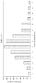
- FIGS. 13A and 13B show the measured frequency dependence of the inductance and the Q factor of all batches of rolled-up device structures without a soft magnetic material in the core (“air-core devices”).
- FIGS. 13C and 13D show the relationship between the inductance and the Q factor versus frequency at frequencies up to 10 MHz for rolled-up electromagnetic components with and without a soft magnetic material in the core.
- FIG. 13E shows the resonant frequency of the Batch 4.2 and 5.2 devices, each of which is above 500 MHz.
- FIG. 13F compares the inductance density by area versus operating frequency of the rolled-up power inductors and other state-of-art planar counterparts from the literature.
- FIG. 13G shows a temperature distribution line scan of a Batch 4 air-core device.
- FIG. 14 shows an exemplary size distribution of iron oxide nanoparticles in a commercially available ferrofluid as determined from a transmission electron microscopy (TEM) image of the iron oxide particles.
- TEM transmission electron microscopy
- Described herein are routes to achieving unprecedented high-density and large current-handling 3D coil structures for magnetic induction using planar semiconductor processing methods and materials.
- the schemes involve geometric transformation of two-dimensional (2D) multilayer sheets or membranes into multi-turn 3D microtubes by self-rolled-up membrane (S-RuM) nanotechnology, and the integration of soft magnetic materials into the core.
- S-RuM self-rolled-up membrane
- milliTesla- and Tesla-level rolled-up magnetic inductors for high power density circuit applications may be fabricated.
- Arrays of the rolled-up magnetic inductors may be able to provide on-chip energy storage via magnetic fields.
- the ⁇ 1 W power capability achieved in experiments suggests that large arrays of the rolled-up inductors may be capable of storing extraordinary power levels and at large power densities.
- the technology may be applicable also to radiofrequency (RF) and millimeter-wave inductors, among other electromagnetic components.
- a more condensed magnetic field distribution and energy storage in 3D space, and thus a higher inductance density, may be achieved for rolled-up electromagnetic components—even those without a magnetic material in the core—than for traditional planar devices.
- the majority of the magnetic field distribution of rolled-up inductors is above the substrate, which provides excellent immunity to parasitic substrate effects.
- rolled-up air-core inductors i.e., rolled-up components with no soft magnetic material in the core
- a set of process strategies are described for achieving milliTesla-(mT) to Tesla-level magnetic induction.
- the integration of a magnetic core in the rolled-up electromagnetic component may result in a 2-times to 1000-times enhancement in the magnetic flux density, depending on factors such as the magnetic properties of the soft magnetic material.
- Soft magnetic materials in contrast to hard magnetic materials, are easily magnetized and demagnetized.
- Soft magnetic materials typically exhibit values of intrinsic coercivity of less than 1000 Nm and have high values of permeability, which is a measure of how readily the material responds to an applied magnetic field.
- Soft magnetic materials are used primarily to enhance and/or channel the flux produced by an electric current.
- FIGS. 1A-1D provide an introduction to the self-rolling concept.
- Rolled-up micro- and nanodevice structures may form spontaneously when planar multilayer sheets including strained layers deform as a consequence of energy relaxation.
- a planar multilayer sheet may include one or more additional layers (not visible in this figure) on an oppositely strained bilayer 140 (e.g., a top sublayer 140 a in tension on a bottom sublayer 140 b in compression), which is in contact with a sacrificial interlayer 145 on a substrate 150 and which may be referred to as a strained layer 140 .
- an oppositely strained bilayer 140 e.g., a top sublayer 140 a in tension on a bottom sublayer 140 b in compression
- the strained layer 140 may be released from the substrate 150 as the sacrificial layer 145 is etched away, as illustrated in FIG. 1C . Once released, the opposing strain within the layer 140 generates a net momentum, driving the planar sheet to scroll up and continue to roll into a tubular structure 100 , as shown in FIG. 1D . During roll-up, residual stress in the strained layer 140 is fully or partially relieved. Accordingly, a rolled portion of the strained layer 140 may be referred to as a strain-relieved layer 140 . Any additional layers can also provide additional residual stress (e.g., tensile stress) to facilitate rolling.
- additional layers can also provide additional residual stress (e.g., tensile stress) to facilitate rolling.
- the electromagnetic component 202 comprises a multilayer sheet 204 in a rolled configuration 206 having at least one turn about a longitudinal axis 208 .
- the multilayer sheet 204 includes a conductive pattern layer 210 on a strain-relieved layer 212 .
- a core 214 of the rolled-up electromagnetic component 202 is defined by a first turn of the rolled configuration 206 , and a soft magnetic material 216 is disposed within the core 214 .
- a magnetic layer 318 , magnetic particles 320 , and/or a solid body 322 may comprise the soft magnetic material 216 , as illustrated in FIGS. 3A-3C .
- the soft magnetic material 216 may take the form of a magnetic layer 318 , magnetic particles 320 , and/or a solid body 322 positioned within the core 214 .
- a rolled-up electromagnetic component 202 may include both a magnetic layer 318 and magnetic particles 320 comprising the soft magnetic material 216 .
- the rolled-up electromagnetic component 202 may be referred to as a rolled-up air-core device structure, or more simply as a rolled-up device structure 240 .
- the rolled-up electromagnetic component 202 may function as a rolled-up inductor, a rolled-up transformer, or a tubular resonant filter.
- rolled-up inductors prepared as described in this disclosure may exhibit an inductance of at least about 5 nH, at least about 7.5 nH, or at least about 1 ⁇ H at a frequency up to 10 MHz.
- the maximum operating frequency of the rolled-up inductors may be about 500 MHz, about 750 MHz, about 1 GHz, or about 5 GHz.
- the rolled-up inductors may exhibit an inductance density as large as 2.5 ⁇ H/mm 2 , as large as 13 pH/mm 3 , or as large as 23 ⁇ H/mm 3 and/or a quality factor of at least about 0.15 or at least about 0.2 at 10 MHz.
- the intensity of the magnetic induction may reach or exceed tens of milliTesla (approaching the Tesla level) in fabricated rolled-up inductors.
- a magnetic layer 318 comprising the soft magnetic material 216 may be disposed on the conductive pattern layer 210 .
- a first portion 318 a of the magnetic layer 318 may be disposed within the core 214 and a remaining portion 318 b of the magnetic layer 318 may surround the core 214 .
- the magnetic layer 318 may partially or fully surround the core 214 in the rolled configuration 206 .
- the soft magnetic material 216 may wrap around the core 214 multiple times depending on the size of the magnetic layer 318 and the number of turns of the rolled configuration 206 .
- the magnetic layer 318 comprising the soft magnetic material 216 may be formed on the conductive pattern layer prior to or after roll-up of the rolled-up electromagnetic component 202 .
- the soft magnetic material 216 may be distributed throughout the core 214 , as illustrated in FIG. 3B , where magnetic particles 320 are packed within the core 214 , or in the example of FIG. 3C , where a monolithic solid body 322 (such as a sintered body prepared from magnetic particles) is disposed within the core 214 .
- the soft magnetic material 216 is uniformly distributed throughout the core 214 .
- the soft magnetic material 216 may be removably positioned within the core 214 . In other words, it may be possible to insert, remove, and/or replace the soft magnetic material 216 as needed.
- a ferrofluid 424 may be employed to deliver the magnetic particles 320 into the core 214 , as illustrated in FIGS. 4A and 4B .
- the ferrofluid 424 may include magnetic particles 320 comprising the soft magnetic material 216 suspended in a carrier fluid 426 , which may comprise an organic or aqueous solvent.
- a delivery needle 428 containing the ferrofluid 424 may be brought adjacent to an end of the rolled-up device structure 240 , as illustrated in FIG. 4A .
- a pendant droplet of the ferrofluid 424 at the tip of the delivery needle 428 may be drawn into the core 214 by capillary forces, partially or completely filling the core 214 , as illustrated in FIG. 4B .
- the ferrofluid 424 may be dried to remove the carrier fluid 426 while the magnetic particles 320 remain stably deposited in the core 214 . Successive droplets of ferrofluid 424 may be delivered into the core 214 as needed, interspersed with drying steps, to increase the packing density of the magnetic particles 320 .
- the multilayer sheet 204 (including the patterned conductive layer 210 and the strain-relieved layer 212 ), the sacrificial layer 218 , an optional protective layer 220 , and the substrate 222 employed for fabrication are described, followed by various embodiments of the soft magnetic material 216 (magnetic layer 318 , magnetic particles 320 , solid body 322 ).
- the conductive pattern layer 210 comprises at least one conductive strip 230 having a length extending in a rolling or circumferential direction, such that the conductive strip(s) 230 wrap around the longitudinal axis 208 in the rolled configuration.
- a plurality of the conductive strips 230 may be disposed along the direction of the longitudinal axis 208 and connected in series by connecting lines 232 , as shown in FIG. 2A and in FIG. 5 .
- Each conductive strip 230 has a width w s and a length L s along the rolling or circumferential direction. As will be discussed further below, the length of each conductive strip 230 may be up to several centimeters in length.
- the length may be as large as about 2 cm, as large as 1 cm, as large as about 50 mm, or as large as about 10 mm.
- the length is at least about 1 mm, at least about 5 mm, or at least about 10 mm.
- the width of each conductive strip may be in a range from about 100 nm to about 500 nm, or from about 200 nm to about 350 nm.
- the conductive pattern layer 210 may also comprise two conductive feed lines 234 connected to the conductive strips 230 to provide a pathway for passage of electrical current therethrough.
- the conductive feed lines 234 may not be part of the rolled configuration 206 ; that is, the conductive feedlines 234 may not wrap around the longitudinal axis 208 . It is also possible that the conductive feed lines may not be present if a signal may be fed to the rolled-up electromagnetic component 202 by other means (e.g., by passive or active components on the chip).
- each of the conductive strips 230 serves as an inductor cell, and the inductance may be maximized when the inductor cells 230 are aligned such that the length of each cell 230 is substantially parallel to (e.g., within ⁇ 1° of) the rolling direction. If the inductor cells 230 are positioned at a non-zero angle with respect to the rolling direction, the inductance may be reduced.
- the conductive pattern layer 210 may comprise one or more conductive materials selected from carbon, silver, gold, aluminum, copper, molybdenum, tungsten, zinc, palladium, platinum, and/or nickel. More typically, the one or more conductive materials may be selected from the group consisting of: carbon, gold, silver, aluminum, palladium, platinum, nickel, and copper.
- a conductive thin film may be deposited on a strained layer by a method such as sputtering or evaporation, and then the conductive thin film may be patterned using lithography and etching steps known in the art to create a conductive pattern.
- the conductive pattern layer 210 has a thickness in a range from about 150 nm to about 300 nm prior to roll-up.
- the conductive pattern layer 210 may comprise a continuous pattern and/or discrete pattern elements.
- the strain-relieved layer 212 (which, prior to roll-up, may be referred to as the strained layer 212 a ) may comprise silicon nitride, silicon oxide, or boron nitride. Typically, the strain-relieved layer 212 (and the strained layer 212 a ) are formed from SiN x (0.5 ⁇ x ⁇ 1.5).
- the strained layer 212 a may be formed by deposition (e.g., CVD) and patterning methods known in the art.
- the strain in the strained layer 212 a may be introduced by compositional or structural differences between sublayers that are successively deposited so as to be in contact with each other.
- adjacent contacting sublayers may be formed with different lattice parameters and/or with different stoichiometries.
- the top sublayer 140 a may have a smaller lattice parameter than the bottom sublayer 140 b , as shown schematically in FIG. 1A .
- the top sublayer 140 a comprises a residual tensile stress
- the bottom sublayer 140 b comprises a residual compressive stress.
- the residual stress profile in the sublayers 140 a , 140 b may be reversed (compressive on top; tensile on bottom) in order to have the rolling proceed downward, instead of upward, which is possible for any of the embodiments described herein. It is also possible that a single layer may be formed with appropriate compositional and/or structural gradients across the layer to produce the desired stress profile in the strained layer. SiN x films deposited by PECVD may differ from single crystal films in that internal strain may be developed not by crystal lattice mismatch but rather by density differences and thermal mismatch achieved by appropriate deposition conditions.
- an oppositely strained SiN x bilayer may be deposited successively with low frequency (e.g., 375 kHz, compressive strain) and high frequency (e.g., 13.56 MHz, tensile strain) PECVD conditions.
- the strained layer may have a residual stress that varies over a wide range, such as from 478 MPa to ⁇ 1100 MPa for silicon nitride (SiN x ) and from greater than 1000 MPa to less than ⁇ 1000 MPa for metal thin films on SiO 2 , where positive values of residual stress correspond to tensile stresses, and negative values correspond to compressive stresses.
- the PECVD environment may be changed by adjusting a ratio of the SiH 4 flow rate to the NH 3 flow rate or by optimizing the power of the RF source.
- the strained layer 212 a has a thickness from about 2 nm to about 200 nm; however, in some embodiments (e.g., in which single crystals are used), the thicknesses may be about 1 nm or less, down to a few monolayers or to one monolayer. Generally, the thickness is at least about 5 nm, at least about 10 nm, at least about 20 nm, at least about 30 nm, at least about 40 nm, or at least about 50 nm. The thickness may also be no more than about 200 nm, no more than about 150 nm, no more than about 100 nm, no more than about 80 nm, no more than about 60 nm, or no more than about 40 nm. When a large number of turns is required and the strained layer 212 a includes two oppositely strained sublayers 236 , 238 (a bilayer), it may be advantageous for the sublayers to have the same thickness, as illustrated in FIG. 2A .
- the sacrificial interlayer (or sacrificial layer) 218 may comprise a material that can be etched without removing or otherwise damaging the strained layer 212 a .
- a material that can be etched without removing or otherwise damaging the strained layer 212 a For example, single-crystalline or polycrystalline Ge, GeO x , Si, and/or AlAs, and/or photoresist, may be used as the sacrificial layer 218 .
- the sacrificial layer 218 has a thickness in a range from about 20 nm to about 200 nm.
- a strained bilayer comprising SiN x may be formed on a sacrificial layer comprising Ge that may be wet etched with hydrogen peroxide or vapor-phase etched with XeF 2 .
- a strained bilayer comprising InAs/GaAs may be formed on a sacrificial layer comprising AlAs that may be etched away with hydrofluoric acid (HF).
- HF hydrofluoric acid
- Deposition and patterning methods known in the art may be employed to form the sacrificial layer 218 on the substrate 222 , which may comprise, for example, a silicon wafer, a silicon-on-insulator wafer, or a sapphire wafer.
- An optional thin protective layer 220 may be deposited on the sacrificial layer 218 to prevent rolling detours or failures caused by pinholes in a strained layer comprising SiN x .
- Suitable materials for the protective layer include alumina (Al 2 O 3 ).
- Such a protective layer 220 may also be applied over the conductive pattern layer as a cover layer.
- Both optional protective/cover layers 220 may have a thickness in a range from about 2 nm to about 30 nm and may be applied using atomic layer deposition (ALD).
- the magnetic layer 318 comprising the soft magnetic material 216 may have a thickness in a range from about 10 nm to about 10 microns. Larger thicknesses (e.g., in a range from about 500 nm (0.5 micron) to about 10 microns) may be achieved by depositing (e.g., electroplating) the magnetic layer post-roll-up, as described below.
- the solid body 322 comprising the soft magnetic material 216 may be sized to fit the core 214 ; in other words, the solid body 322 may have dimensions determined by the length and/or diameter of the core 214 formed during roll-up.
- the length of the core 214 may be determined or influenced by the geometry of the conductive pattern layer 210 (e.g., the width, spacing, and number of conductive strips) and may vary over a wide range, such as from about 10 microns to about 8000 microns (8 mm).
- the length of the solid body 322 may be least about 10 microns, at least about 50 microns, at least about 100 microns, at least about 200 microns, or at least about 500 microns, and the length may also be about 8000 microns or less, about 5000 microns or less, or about 1000 microns or less.
- the diameter of the core 214 upon roll-up depends on the thickness of the multilayer sheet 204 as well as the amount of strain in the strained layer 212 a prior to release of the sacrificial layer 218 .
- a thicker multilayer sheet 204 may tend to roll to a larger inner diameter; however, a higher level of strain in the strained layer 212 a can offset this effect, since the inner diameter (D) of the rolled configuration 206 is proportional to the thickness (t) of the multilayer sheet 204 and is inversely proportional to the amount of strain ( ⁇ ) therein (D ⁇ t/ ⁇ ).
- the core 214 has a diameter in a range from about 1 micron to about 1000 microns.
- the solid body 322 may have a diameter no more than about 1000 microns, no more than about 500 microns, no more than about 300 microns, or no more than about 100 microns.
- the diameter of the solid body 322 may also be at least about 1 micron, at least about 5 microns, or at least about 10 microns.
- Magnetic particles 320 comprising the soft magnetic material 216 may have a spherical, irregular, cubic, polygonal, anisotropic, acicular, two-dimensional, and/or plate-like morphology.
- the magnetic particles 320 have a nominal size in a range from about 1 nm to about 10 microns, from 1 nm to about 1 micron, or from 1 nm to about 100 nm. Smaller magnetic particles 320 may be advantageous for reducing magnetic dipole-dipole interactions and maintaining a uniform dispersion within a ferrofluid 424 used to deliver the magnetic particles 320 into the core 214 .
- the nominal size of the magnetic particles 320 is preferably in a range from about 1 nm to about 20 nm, or from about 1 nm to about 10 nm.
- the soft magnetic material 216 may comprise iron oxide, such as Fe 2 O 3 or Fe 3 O 4 , a ferrite such as a nickel ferrite, manganese ferrite, zinc ferrite, or cobalt ferrite, iron nitride, manganese selenide, a ferromagnetic metal or alloy, such as iron, nickel, cobalt, a nickel-iron alloy such as permalloy, and/or an iron-silicon-aluminum alloy, such as sendust.
- iron oxide such as Fe 2 O 3 or Fe 3 O 4
- a ferrite such as a nickel ferrite, manganese ferrite, zinc ferrite, or cobalt ferrite, iron nitride, manganese selenide, a ferromagnetic metal or alloy, such as iron, nickel, cobalt, a nickel-iron alloy such as permalloy, and/or an iron-silicon-aluminum alloy, such as sendust.
- Exemplary ferrites may include ZnFe 2 O 4 , MnFe 2 O 4 , NiFe 2 O 4 , CoFe 2 O 4 , Co x Ni 1-x Fe 2 O 4 , Co x Zn 1-x Fe 2 O 4 , Ni x Zn 1-x Fe 2 O 4 , and/or Mn x Zn 1-x Fe 2 O 4 , where 0 ⁇ x ⁇ 1.
- Ferrites or metals/alloys may be preferred over iron oxide for higher frequency applications.
- a ferrofluid 424 may be employed to deliver the magnetic particles 320 into the core 214 .
- the ferrofluid 424 may comprise the magnetic particles 320 suspended in a carrier fluid 426 , which may be an aqueous or organic solvent such as water, hexane, acetone, isopropanol, butanol, benzyl alcohol, and/or pentanol.
- a carrier fluid 426 may be an aqueous or organic solvent such as water, hexane, acetone, isopropanol, butanol, benzyl alcohol, and/or pentanol.
- the magnetic particles 320 may be present in the ferrofluid 424 at concentration of at least about 15 vol. %, at least about 30 vol. %, or at least about 40 vol. %
- the magnetic particles 320 may be functionalized with surface ligands, such as hydrocarbon ligands, and/or charged groups.
- the dielectric constant of the carrier fluid 426 may be “matched” with that of the magnetic particles 320 ; for example, the carrier fluid 426 may have a dielectric constant within ⁇ 40% of the dielectric constant of the magnetic particles 320 , or within ⁇ 20% of the dielectric constant of the magnetic particles 320 .
- Fe 2 O 3 nanoparticles have a dielectric constant of 14.2, for example, and dielectric constants of exemplary carrier fluids are provided in Table 1 below. With sufficient matching of dielectric constants, a homogeneous and stable ferrofluid 424 may be obtained.
- the ferrofluid 424 may have a saturation magnetization (M s ) of at least about 99 mT, at least about 500 mT, or at least about 1 T, and/or as high as about 5 T.
- M s saturation magnetization
- the ferrofluid 424 may also or alternatively exhibit a maximum working frequency of at least about 450 MHz, at least about 700 MHz, or at least about 1 GHz, and/or as high as 5 GHz.
- the ferrofluid 424 may also or alternatively have an initial magnetic susceptibility of at least about 18, at least about 100, at least about 500, or at least about 1000 (SI units).
- conductive strips 230 to be rolled-up may be tens of times longer than in previous work (e.g., up to several millimeters or up to 1-2 cm) and larger in cross sectional area (e.g., tens of square micrometers) for higher coil density and lower DC resistance, respectively.
- a conductive pattern layer 210 having a thickness that can be successfully rolled up may undergo a post-roll-up electroplating process to increase the thickness of the conductive pattern layer 210 to the microscale (e.g., from about 1 micron up to 10 microns).
- a conductive material may be directed into the core 214 and into the gaps between adjacent turns, such that the conductive material is deposited on and increases the thickness of the conductive pattern layer 210 .
- This considerable thickness increase in combination with (or as an alternative to) increasing the length and/or width of the conductive strips 230 as described above, may allow for a reduced DC resistance to be achieved without impairing the roll-up process.
- a method of making a rolled-up electromagnetic component includes forming 610 a rolled-up device structure comprising: a multilayer sheet in a rolled configuration comprising at least one or multiple turns about a longitudinal axis, the multilayer sheet comprising a conductive pattern layer on a strain-relieved layer; and a core defined by a first turn of the rolled configuration; and introducing 620 a soft magnetic material into the core.
- a ferrofluid including magnetic particles comprising the soft magnetic material may be delivered 630 into the core.
- a magnetic layer may be formed 640 on the conductive pattern layer within the core before and/or after roll-up.
- a solid body comprising the soft magnetic material may be inserted 650 into the core. It can be beneficial to introduce the soft magnetic material into the core after roll-up due to the practical challenges inherent to rolling up a multilayer sheet of an excessive thickness.
- the rolled configuration comprises multiple turns about the longitudinal axis.
- the soft magnetic material may be introduced into the core during roll-up.
- the soft magnetic material may be introduced into the core after the first turn but prior to completion of roll-up for a device structure having more than one turn.
- a magnetic layer comprising the soft magnetic material may be deposited on the conductive pattern layer prior to roll-up, and thus the soft magnetic material may be incorporated into the core during roll-up.
- an object or layer (such as the magnetic layer) which is described in this disclosure as being formed on, deposited on, disposed on or otherwise applied onto a different layer (such as the conductive pattern layer) may be understood to be formed directly on (i.e., in physical contact with) the different layer, or directly on an intervening layer which is on (or directly on) the different layer.
- introducing the soft magnetic material 216 into the core 214 may entail positioning a tip of a delivery needle 428 containing a ferrofluid 424 adjacent to the core 214 at an end of the rolled-up device structure 240 , where the tip includes a pendant drop (a suspended droplet) of the ferrofluid 424 .
- the droplet and the end of the rolled-up device structure 240 are brought into contact, and capillary forces induce the ferrofluid 424 to flow into the core 214 .
- Bringing the droplet and the end of the rolled-up device structure 240 into contact may entail bringing the tip of the delivery needle into contact with the end of the rolled-up device structure 240 .
- the delivery needle 428 may be removed. Following delivery, the ferrofluid 424 may remain stably confined inside the core 214 .
- the ferrofluid 424 may be dried to remove the carrier fluid 426 , leaving the magnetic particles 320 packed within the core 214 of the rolled-up electromagnetic component 202 . The process may be repeated one or more times to increase the packing density of magnetic particles 320 deposited in the core 214 .
- the drying to remove the carrier fluid 426 may comprise active and/or passive drying.
- the carrier fluid 426 may evaporate under ambient conditions (i.e., room temperature (about 20-25° C.) and atmospheric pressure). Alternatively, the drying may entail heating of the ferrofluid 424 and/or providing a forced gas flow over the electromagnetic component 202 .
- the soft magnetic material 216 may be introduced into the core 214 by a deposition process such as electroplating, which may also be referred to as electrodeposition.
- fabrication of the rolled-up device structure 240 may include an additional step of incorporating spacers 700 on the thin film layers prior to roll-up, as described below, in order to produce a rolled-up device structure 240 with spaced-apart adjacent turns, as shown in FIGS. 7A and 7B .
- the soft magnetic material 216 and/or a conductive material 720 may be directed into spaces 710 between adjacent turns and onto the conductive pattern layer 210 by a process such as electroplating. Accordingly, the spaces 710 between adjacent turns may be partially or completely filled with the desired material (e.g., the soft magnetic material 216 and/or a conductive material 720 ), as illustrated in FIG. 7C .
- a two-electrode electroplating system with a cathode electrically connected to one or more rolled-up device structures (e.g., on a sapphire wafer) and an anode in a suitable electroplating solution may be employed for electrodeposition.
- Suitable electroplating solutions may be selected depending on the metal or alloy to be deposited and may be obtained commercially (e.g., from Transene Company, Inc., Danvers, Mass.) or prepared using on recipes known in the art.
- electrolytic conditions e.g., solution composition, pH, temperature, and current density
- Electroplating may also or alternatively be used to increase the thickness of the conductive pattern layer.
- electroplating may be carried out using a different electroplating solution suitable for depositing the conductive material of the conductive pattern layer instead of the soft magnetic material of the magnetic layer.
- two (or more) electroplating steps may be carried out.
- a first electroplating step may be employed using a suitable electroplating solution to increase the thickness of the conductive pattern layer
- a second electroplating step may be employed using a suitable electroplating solution for depositing the soft magnetic material to form the magnetic layer.
- the thickness of the magnetic layer and/or the conductive layer may be controlled by the time duration of the electroplating process.
- electroplating is carried out at room temperature, but the electroplating system may be equipped with a heating element for controlled heating during electrodeposition if desired.
- FIGS. 8A-8F illustrate an exemplary fabrication process through roll-up.
- a sacrificial layer e.g., Ge layer
- a strained layer e.g., SiN x bilayer
- the layers are shown prior to patterning in FIG. 8A ; in FIG. 8B the layers have been patterned to form a “mesa” structure.
- the sacrificial layer 218 has a relatively large Young's modulus to avoid absorbing strain energy from the strained layer 212 a .
- the sacrificial layer 218 preferably also has a smooth surface to avoid decreasing the conductivity of the copper layer from surface roughness accumulation.
- a thin protective layer (not visible) comprising alumina (Al 2 O 3 ), for example, may be deposited on the sacrificial layer 218 beneath the strained layer 212 a to address the pinhole issue associated with the strained layer 212 a .
- the strained layer 218 may comprise an upper portion 238 under tensile stress and a lower portion 236 under compressive stress, and the strained layer 212 a may be held on the substrate 222 by the sacrificial layer 218 .
- the compressive and tensile stresses may be formed in the strained layer by low frequency (LF) PECVD (to form the lower portion 236 ) and by high frequency (HF) PECVD (to form the upper portion 238 ).
- the compressive and tensile stresses may be maximized to provide sufficient rolling force to roll up a relatively thick conductive pattern layer (e.g., copper layer) 210 , which, as shown in FIGS. 8C and 8D , is formed on the strained layer 212 a .
- a cover layer e.g., Al 2 O 3 layer
- the conductive pattern layer 210 may comprise at least one conductive strip 230 having a length extending in a rolling direction. There may be an even number of conductive strips 230 deposited on the strained layer 210 and linked together by short connecting lines.
- the thickness of the conductive (e.g., Cu) strips 230 is from 150 nm to 250 nm with a width of from 250 ⁇ m to 300 ⁇ m, which yields a cross-sectional area from 37.5 ⁇ m 2 to 75 ⁇ m 2
- the number of conductive strips 230 may be chosen to be an even number up to six. Long and wide conductive strips are beneficially used because of the difficulty of rolling up micron-thick conductive strips 230 , as discussed above. However, an undesirable corner effect may be introduced when the conductive strip 230 is excessively wide; thus, a rounded corner design of the conductive strips may be used to address this issue.
- removal of the sacrificial layer 218 from the substrate 222 may be initiated in order to release an end of the strained layer 212 a , and the removal of the sacrificial layer 218 may be continued, thereby allowing the strained layer 212 a to move away from the substrate 222 and roll up to relieve strain.
- the removal of the sacrificial layer 218 may entail wet or dry etching, as described below.
- the conductive pattern layer 210 adheres to the strained layer 212 a during roll-up, and a rolled-up device structure 240 is formed.
- a first lithography step is used to define the mesa, as shown in FIG. 8B .
- a second lithography step is used to define the 2D size and shape of the conductive pattern layer, as shown in FIG. 8C , which comprises two conductive strips in this example.
- a final lithography step in FIG. 8E opens an etching window on a far end of the mesa through a cover layer (e.g., Al 2 O 3 layer) to facilitate etching of the sacrificial layer and realize directional rolling.
- a cover layer e.g., Al 2 O 3 layer
- a critical enabler of the scaling scheme to roll up centimeter-scale and and longer conductive strips to increase the number of turns is to use a dry etching approach (e.g., gaseous xenon difluoride (XeF 2 )) to release the sacrificial layer, which in these examples comprise Ge, instead of using traditional wet etching solutions.
- the dry etching releasing yields a rolling speed of up to about 750 ⁇ m/min, which is over 500 times faster than wet etching methods and provides the rolling momentum for a much heavier load, such as conductive strips of up to hundreds of nanometers in thickness, up to hundreds of microns in width, and up to one or more centimeters in length.
- the super-fast dry releasing speed may avoid the problems of detouring and failure associated with pinholes in the SiN x strained layers, even without a protective (e.g., Al 2 O 3 ) layer when the rolling length is under 1 mm long.
- a protective e.g., Al 2 O 3
- the above-described fabrication process may be modified to incorporate discrete bumps on the strained layer (e.g., directly on the strained layer, the conductive pattern layer, and/or the optional spacer layer), as mentioned above and as illustrated in FIG. 9 , to serve as spacers during roll-up. Consequently, the rolled-up device structures shown in FIGS. 7A and 7B may be formed.
- S-RuM power inductors with diverse geometry parameters and wide-ranging electrical performance can be realized in many different two-dimensional layout designs using a variety of core materials. Described here are five batches of S-RuM power inductors, where each is fabricated with a conductive pattern layer comprising Cu and having a thickness in a range from 150 nm to 225 nm. The batches have different numbers of cells (2 or 6) where each cell has the same width of 250 microns but different lengths scaled from 0.8 mm to 10 mm.
- FIG. 10 is a length comparison of all batches before rolling, where the images show a top-down view of the conductive pattern layer deposited on a strained layer for Batches 1-5.
- FIG. 10 Provided in FIG. 10 is a length comparison of all batches before rolling, where the images show a top-down view of the conductive pattern layer deposited on a strained layer for Batches 1-5.
- FIG. 11 shows scanning electron microscope (SEM) images of Batch 1, 2 and 4 rolled-up device structures having from about 1.5 to about 21 turns. The largest number of turns is obtained from the Batch 5 design (10 mm long conductive strip), which yields rolled-up device structures with up to 23 turns and an inner diameter of about 140 microns.
- FIGS. 4A and 4B described above illustrate a controllable core-filling process to fill the cores of the rolled-up device structures with ferrofluid to form rolled-up electromagnetic components, such as rolled-up power inductors.
- the ferromagnetic fluid is drawn into a 28-gauge micropipette (delivery needle) by capillary action, with a droplet suspended from the tip of the pipette. Then, the pipette is lowered until it is nearly level with the rolled-up device structure and is moved towards an end of the device structure to make contact.
- FIG. 12 A 3 ⁇ 3 array of fully fabricated and core-filled 2-cell S-RuM rolled-up inductors are shown in FIG. 12 .
- FIGS. 13A and 13B The measured frequency dependence of the inductance and the Q factor of all batches of devices without the core filled (“air-core devices”) is shown in FIGS. 13A and 13B .
- inductance shows a superlinear relationship with the number of turns.
- the Batch 5.2 device has an inductance as large as 140 nH at 10 MHz, a maximum working frequency at 2 GHz, and a maximum Q factor of 2.3 at 250 MHz.
- the inductance per cell is improved by 46.7 times by increasing the length of the Cu strip by 12.5 times.
- the resonance frequency continues to drop from Batch 1 (>20 GHz) to Batch 5.2 (>1.3 GHz) but with rapidly decreasing rate due to the weakened influence of crosstalk coupling capacitance between turns.
- the maximum Q factor at 250 MHz is ⁇ 2.85, improved by 11.4 times from the previously reported best result of ⁇ 0.25, due to the use of vapor-phase releasing, which enables roll-up of large cross-sectional-area Cu strips.
- the operating frequency exhibits a drop due to the ferromagnetic resonance of the iron oxide nanoparticles used for this experimental study.
- the data collected with a Keithley Clarius and CMT VNA are combined in FIGS. 13C and 13D to show the relationship between the inductance and the Q factor versus frequency. It can be seen that the inductance reaches 1.24 ⁇ H at 10 KHz and the maximum Q factor is 0.9 at 10 MHz for the Batch 5.2 device.
- the enhanced magnetic flux by ferrofluid at low frequency is about 9 times and 3 times, respectively, for the maximum inductance and the Q factor.
- the improvement in the Q factor is not as much as that of the inductance because of ferromagnetic resonance loss (FMR).
- FMR ferromagnetic resonance loss
- FIG. 13E shows the resonant frequency of the Batch 4.2 and 5.2 devices, which are both above 500 MHz. Compared to bulk iron oxide material, monodomain iron oxide nanoparticles have a much large FMR frequency, which suggests an important application when both high power and high frequency are required.
- FIG. 13F compares the inductance density by area versus operating frequency between the S-RuM power inductor devices and other state-of-art planar counterparts from the literature (labeled 47-51). Clearly, the S-RuM devices show much higher inductance density across the entire frequency range and a unique capability in high frequency operation, which satisfies the requirement of a switching frequency range of 100 MHz to 500 MHz for the next generation of power devices. As discussed above, the performance can be further improved by simply scaling the conductive strips to longer lengths and/or widths and/or to materials with better conductivity.
- FIG. 13G Shown in FIG. 13G is a temperature distribution line scan of a Batch 4 air-core device.
- the background temperature is set to be 50° C. in order to obtain a reasonable signal to noise ratio.
- the input current is set to 250 mA with measured maximum temperature of about 400° C. without destroying the device.
- the data indicate that the maximum power of the Batch 4 SRuM power inductor should be above 0.94 W with a corresponding power density of about 8.5 W/mm 2 and a maximum magnetic induction of 12 mTesla in the core.
- Patterning to define mesa Spin on positive photoresist (“PR,” AZ5214E); spin on HMDS; soft bake 1 min at 110° C.; expose with 320 nm UV lithography with optical photo mask; develop in MIF 917 developer for 75 sec; O 2 descum for PR residual removal; reactive ion etching with CF 4 , 30 sccm gas flow, 90 W power, 35 mTorr pressure, for 6 mins; acetone, methanol, isopropanol rinse to strip PR, DI water rinse, N 2 drying; O 2 descum for PR residual removal.
- PR positive photoresist
- HMDS spin on HMDS
- soft bake 1 min at 110° C. expose with 320 nm UV lithography with optical photo mask; develop in MIF 917 developer for 75 sec; O 2 descum for PR residual removal; reactive ion etching with CF 4 , 30 sccm gas flow, 90 W power, 35 mTorr pressure, for 6 mins;
- Conductive pattern (Cu) layer deposition Spin on image reversal photoresist (AZ5214E-IR); spin on HMDS; soft bake 1 min at 110° C.; expose for 9 secs by 320 nm UV lithography with optical photo mask; reversal bake 1 min at 110° C.; flood exposure for 1 min by 320 nm UV lithography; develop in MIF 917 developer for 75 sec; O 2 descum for PR residual removal; ion descum in HCl for 2 mins; 5 nm Ni followed by 180 nm Cu deposited by electron beam evaporation; metal lift-off in AZ 400T stripper for 20 mins.
- FIG. 14 shows the size distribution of the iron oxide nanoparticles as determined from a transmission electron microscopy (TEM) image of the EMG 900 nanoparticles.
- TEM transmission electron microscopy
Landscapes
- Engineering & Computer Science (AREA)
- Power Engineering (AREA)
- Soft Magnetic Materials (AREA)
- Coils Or Transformers For Communication (AREA)
Abstract
Description
| TABLE 1 |
| Exemplary Carrier Fluids and Dielectric Constants |
| Carrier Fluid | Dielectric Constant | ||
| Water | 80.1 | ||
| Hexane | 1.9 | ||
| |
21 | ||
| |
22, 19 | ||
| Butanol | 17.5 | ||
| |
13 | ||
| |
14, 13.7, 3.3 | ||
| TABLE 2 |
| Primary Dimensional Parameters of Exemplary S-RuM Inductors |
| Cu | Cu | Cu | # | Al2O3 | Al2O3 | |||
| Batch | strip | strip | strip | Inner | of | cover | underneath | |
| # | thickness | width | length | diameter | | layer | layer | |
| 1 | 250 μm | 0.8 mm | 165 |
2 | 15 |
0 | |
| 2 | 150 |
250 μm | 1.6 mm | 165 |
2 | 15 |
0 |
| 3 | 225 |
300 nm | 3.2 |
200 |
2 | 15 |
0 |
| 4.1 | 150 |
300 nm | 6.4 |
180 |
2 | 25 |
0 |
| 4.2 | 180 |
300 nm | 6.4 |
140 |
4 | 20 |
5 |
| 5.1 | 180 |
300 |
10 |
140 |
4 | 20 |
5 |
| 5.2 | 180 |
300 |
10 |
140 |
6 | 20 |
5 |
Claims (19)
Priority Applications (1)
| Application Number | Priority Date | Filing Date | Title |
|---|---|---|---|
| US16/434,524 US11031456B2 (en) | 2018-06-08 | 2019-06-07 | Rolled-up electromagnetic component for on-chip applications and method of making a rolled-up electromagnetic component |
Applications Claiming Priority (2)
| Application Number | Priority Date | Filing Date | Title |
|---|---|---|---|
| US201862682569P | 2018-06-08 | 2018-06-08 | |
| US16/434,524 US11031456B2 (en) | 2018-06-08 | 2019-06-07 | Rolled-up electromagnetic component for on-chip applications and method of making a rolled-up electromagnetic component |
Publications (2)
| Publication Number | Publication Date |
|---|---|
| US20190378890A1 US20190378890A1 (en) | 2019-12-12 |
| US11031456B2 true US11031456B2 (en) | 2021-06-08 |
Family
ID=68765304
Family Applications (1)
| Application Number | Title | Priority Date | Filing Date |
|---|---|---|---|
| US16/434,524 Active US11031456B2 (en) | 2018-06-08 | 2019-06-07 | Rolled-up electromagnetic component for on-chip applications and method of making a rolled-up electromagnetic component |
Country Status (1)
| Country | Link |
|---|---|
| US (1) | US11031456B2 (en) |
Cited By (2)
| Publication number | Priority date | Publication date | Assignee | Title |
|---|---|---|---|---|
| US20220119976A1 (en) * | 2020-10-19 | 2022-04-21 | The Board Of Trustees Of The University Of Illinois | Electroplating Method for Enhancing the Performance of Rolled-Up Passive Components |
| US11444148B2 (en) * | 2018-12-17 | 2022-09-13 | Intel Corporation | Recoiled metal thin film for 3D inductor with tunable core |
Families Citing this family (1)
| Publication number | Priority date | Publication date | Assignee | Title |
|---|---|---|---|---|
| CN115893308B (en) * | 2023-02-14 | 2026-04-21 | 合肥工业大学 | A fabrication method for GMI magnetic sensors based on thin-film self-rolling technology |
Citations (5)
| Publication number | Priority date | Publication date | Assignee | Title |
|---|---|---|---|---|
| US20140103486A1 (en) * | 2012-10-11 | 2014-04-17 | The Board Of Trustees Of The University Of Illinois | Rolled-up inductor structure for a radiofrequency integrated circuit (rfic) |
| US20150099116A1 (en) | 2013-10-09 | 2015-04-09 | The Board Of Trustees Of The University Of Illinois | Chiral structure, method of making a chiral structure, and rolled-up structure with modulated curvature |
| US20160301377A1 (en) | 2015-04-08 | 2016-10-13 | The Board Of Trustees Of The University Of Illinois | Tubular resonant filter and method of making a tubular resonant filter |
| US20180012695A1 (en) * | 2016-07-07 | 2018-01-11 | Hyundai Motor Company | Molding inductor |
| US20180075956A1 (en) | 2016-09-15 | 2018-03-15 | The Board Of Trustees Of The University Of Illinois | Rolled-Up Power Inductor and Array of Rolled-Up Power Inductors for On-Chip Applications |
-
2019
- 2019-06-07 US US16/434,524 patent/US11031456B2/en active Active
Patent Citations (7)
| Publication number | Priority date | Publication date | Assignee | Title |
|---|---|---|---|---|
| US20140103486A1 (en) * | 2012-10-11 | 2014-04-17 | The Board Of Trustees Of The University Of Illinois | Rolled-up inductor structure for a radiofrequency integrated circuit (rfic) |
| US20140246764A1 (en) | 2012-10-11 | 2014-09-04 | The Board Of Trustees Of The University Of Illinoi | Rolled-up transmission line structure for a radiofrequency integrated circuit (rfic) |
| US20150137930A1 (en) | 2012-10-11 | 2015-05-21 | The Board Of Trustees Of The University Of Illinois | Rolled-up transformer structure for a radiofrequency integrated circuit (rfic) |
| US20150099116A1 (en) | 2013-10-09 | 2015-04-09 | The Board Of Trustees Of The University Of Illinois | Chiral structure, method of making a chiral structure, and rolled-up structure with modulated curvature |
| US20160301377A1 (en) | 2015-04-08 | 2016-10-13 | The Board Of Trustees Of The University Of Illinois | Tubular resonant filter and method of making a tubular resonant filter |
| US20180012695A1 (en) * | 2016-07-07 | 2018-01-11 | Hyundai Motor Company | Molding inductor |
| US20180075956A1 (en) | 2016-09-15 | 2018-03-15 | The Board Of Trustees Of The University Of Illinois | Rolled-Up Power Inductor and Array of Rolled-Up Power Inductors for On-Chip Applications |
Non-Patent Citations (50)
Cited By (3)
| Publication number | Priority date | Publication date | Assignee | Title |
|---|---|---|---|---|
| US11444148B2 (en) * | 2018-12-17 | 2022-09-13 | Intel Corporation | Recoiled metal thin film for 3D inductor with tunable core |
| US20220119976A1 (en) * | 2020-10-19 | 2022-04-21 | The Board Of Trustees Of The University Of Illinois | Electroplating Method for Enhancing the Performance of Rolled-Up Passive Components |
| US12442101B2 (en) * | 2020-10-19 | 2025-10-14 | The Board Of Trustees Of The University Of Illinois | Electroplating method for enhancing the performance of rolled-up passive components |
Also Published As
| Publication number | Publication date |
|---|---|
| US20190378890A1 (en) | 2019-12-12 |
Similar Documents
| Publication | Publication Date | Title |
|---|---|---|
| US9224532B2 (en) | Rolled-up inductor structure for a radiofrequency integrated circuit (RFIC) | |
| US11031456B2 (en) | Rolled-up electromagnetic component for on-chip applications and method of making a rolled-up electromagnetic component | |
| Pirota et al. | Novel magnetic materials prepared by electrodeposition techniques: arrays of nanowires and multi-layered microwires | |
| Narayanan et al. | Hybrid multiferroic nanostructure with magnetic–dielectric coupling | |
| Su et al. | Self-assembled magnetic metallic nanopillars in ceramic matrix with anisotropic magnetic and electrical transport properties | |
| CN112216469B (en) | Magnetic laminate, magnetic structure comprising same, electronic component comprising laminate or structure, and method for producing magnetic laminate | |
| US11948719B2 (en) | Nanomagnetic inductor cores, inductors and devices incorporating such cores, and associated manufacturing methods | |
| JP2014525138A (en) | Magnetostrictive layer system | |
| JP2008192645A (en) | Thin film magnetic device and manufacturing method thereof | |
| Guo et al. | Self‐Rolling‐Up Enabled Ultrahigh‐Density Information Storage in Freestanding Single‐Crystalline Ferroic Oxide Films | |
| US7482727B2 (en) | Composite material with conductive nanowires | |
| US20070188920A1 (en) | Microinductor and fabrication method thereof | |
| JP2009245959A (en) | Electromagnetic energy storage or release device using spin dynamics, and method of manufacturing the same | |
| CN112635657B (en) | A wireless energy harvesting system, a spin diode and a method for preparing the same | |
| CN116884728A (en) | Magnetic soliton generating device and generating method | |
| Lai et al. | Suspended nanoscale solenoid metal inductor with tens-nH level inductance | |
| KR101768860B1 (en) | Giant magnetoresistance device using graphene/ferroelectric junction structure, and fabrication method of the same | |
| CN111573618A (en) | In-situ integrated three-dimensional nanowire helical loop magnetic head, preparation method and use thereof | |
| Vrejoiu et al. | Ferroelectric nanostructures | |
| Kraman | Ferrofluid-core S-RuM microelectronic inductors | |
| US12442101B2 (en) | Electroplating method for enhancing the performance of rolled-up passive components | |
| Rashid | The use of nano photoelectric process in the production of electronic nanowires | |
| Dastagir et al. | Templated fabrication and characterization of SiO2 nanotube covered Fe nanowires | |
| CN121368335A (en) | Magnetic domain storage device on self-curling sheet and preparation method | |
| Riaz et al. | Fabrication and magnetic characterization of AAO template assisted growth of Fe3O4 nanotubes |
Legal Events
| Date | Code | Title | Description |
|---|---|---|---|
| FEPP | Fee payment procedure |
Free format text: ENTITY STATUS SET TO UNDISCOUNTED (ORIGINAL EVENT CODE: BIG.); ENTITY STATUS OF PATENT OWNER: SMALL ENTITY |
|
| FEPP | Fee payment procedure |
Free format text: ENTITY STATUS SET TO SMALL (ORIGINAL EVENT CODE: SMAL); ENTITY STATUS OF PATENT OWNER: SMALL ENTITY |
|
| STPP | Information on status: patent application and granting procedure in general |
Free format text: DOCKETED NEW CASE - READY FOR EXAMINATION |
|
| STPP | Information on status: patent application and granting procedure in general |
Free format text: NON FINAL ACTION MAILED |
|
| AS | Assignment |
Owner name: NATIONAL SCIENCE FOUNDATION, VIRGINIA Free format text: CONFIRMATORY LICENSE;ASSIGNOR:UNIVERSITY OF ILLINOIS, URBANA-CHAMPAIGN;REEL/FRAME:054414/0546 Effective date: 20200219 |
|
| STPP | Information on status: patent application and granting procedure in general |
Free format text: RESPONSE TO NON-FINAL OFFICE ACTION ENTERED AND FORWARDED TO EXAMINER |
|
| STPP | Information on status: patent application and granting procedure in general |
Free format text: NOTICE OF ALLOWANCE MAILED -- APPLICATION RECEIVED IN OFFICE OF PUBLICATIONS |
|
| AS | Assignment |
Owner name: THE BOARD OF TRUSTEES OF THE UNIVERSITY OF ILLINOIS, ILLINOIS Free format text: ASSIGNMENT OF ASSIGNORS INTEREST;ASSIGNORS:LI, XIULING;HUANG, WEN;YANG, ZHENDONG;AND OTHERS;SIGNING DATES FROM 20190610 TO 20210507;REEL/FRAME:056175/0742 |
|
| STPP | Information on status: patent application and granting procedure in general |
Free format text: PUBLICATIONS -- ISSUE FEE PAYMENT RECEIVED |
|
| STPP | Information on status: patent application and granting procedure in general |
Free format text: PUBLICATIONS -- ISSUE FEE PAYMENT VERIFIED |
|
| STCF | Information on status: patent grant |
Free format text: PATENTED CASE |
|
| AS | Assignment |
Owner name: NATIONAL SCIENCE FOUNDATION, VIRGINIA Free format text: CONFIRMATORY LICENSE;ASSIGNOR:UNIVERSITY OF ILLINOIS;REEL/FRAME:063593/0233 Effective date: 20200216 |
|
| MAFP | Maintenance fee payment |
Free format text: PAYMENT OF MAINTENANCE FEE, 4TH YR, SMALL ENTITY (ORIGINAL EVENT CODE: M2551); ENTITY STATUS OF PATENT OWNER: SMALL ENTITY Year of fee payment: 4 |