US11025200B2 - Magnetic coupling layers, structures comprising magnetic coupling layers and methods for fabricating and/or using same - Google Patents
Magnetic coupling layers, structures comprising magnetic coupling layers and methods for fabricating and/or using same Download PDFInfo
- Publication number
- US11025200B2 US11025200B2 US16/562,337 US201916562337A US11025200B2 US 11025200 B2 US11025200 B2 US 11025200B2 US 201916562337 A US201916562337 A US 201916562337A US 11025200 B2 US11025200 B2 US 11025200B2
- Authority
- US
- United States
- Prior art keywords
- magnetic
- layer
- coupling
- magnetization direction
- magnetic layer
- Prior art date
- Legal status (The legal status is an assumption and is not a legal conclusion. Google has not performed a legal analysis and makes no representation as to the accuracy of the status listed.)
- Active
Links
- 230000005291 magnetic effect Effects 0.000 title claims abstract description 995
- 238000010168 coupling process Methods 0.000 title claims abstract description 716
- 238000005859 coupling reaction Methods 0.000 title claims abstract description 716
- 230000008878 coupling Effects 0.000 title claims abstract description 715
- 238000000034 method Methods 0.000 title claims description 32
- 230000005415 magnetization Effects 0.000 claims abstract description 255
- 230000005290 antiferromagnetic effect Effects 0.000 claims description 53
- 229910052742 iron Inorganic materials 0.000 claims description 39
- 238000000137 annealing Methods 0.000 claims description 38
- 229910052759 nickel Inorganic materials 0.000 claims description 33
- 230000008859 change Effects 0.000 claims description 32
- 229910052707 ruthenium Inorganic materials 0.000 claims description 27
- 229910045601 alloy Inorganic materials 0.000 claims description 26
- 239000000956 alloy Substances 0.000 claims description 26
- 229910052804 chromium Inorganic materials 0.000 claims description 24
- 239000000203 mixture Substances 0.000 claims description 24
- 229910052741 iridium Inorganic materials 0.000 claims description 23
- 229910052702 rhenium Inorganic materials 0.000 claims description 22
- 229910052703 rhodium Inorganic materials 0.000 claims description 22
- 229910052715 tantalum Inorganic materials 0.000 claims description 17
- 229910052782 aluminium Inorganic materials 0.000 claims description 16
- 229910052758 niobium Inorganic materials 0.000 claims description 16
- 229910052721 tungsten Inorganic materials 0.000 claims description 16
- 229910052720 vanadium Inorganic materials 0.000 claims description 16
- 229910052802 copper Inorganic materials 0.000 claims description 15
- 229910052748 manganese Inorganic materials 0.000 claims description 15
- 229910052710 silicon Inorganic materials 0.000 claims description 15
- 229910052719 titanium Inorganic materials 0.000 claims description 15
- 230000004044 response Effects 0.000 claims description 13
- 229910052709 silver Inorganic materials 0.000 claims description 12
- 150000001875 compounds Chemical class 0.000 claims description 8
- 230000001419 dependent effect Effects 0.000 claims description 8
- 229910052750 molybdenum Inorganic materials 0.000 claims description 7
- 230000008569 process Effects 0.000 claims description 7
- 229910018979 CoPt Inorganic materials 0.000 claims description 6
- 229910000684 Cobalt-chrome Inorganic materials 0.000 claims description 6
- 239000010952 cobalt-chrome Substances 0.000 claims description 6
- 229910018936 CoPd Inorganic materials 0.000 claims description 4
- 229910005335 FePt Inorganic materials 0.000 claims description 4
- 238000000231 atomic layer deposition Methods 0.000 claims description 4
- 238000005240 physical vapour deposition Methods 0.000 claims description 4
- 229910015187 FePd Inorganic materials 0.000 claims description 3
- 238000000151 deposition Methods 0.000 claims 7
- 238000005229 chemical vapour deposition Methods 0.000 claims 2
- 239000000126 substance Substances 0.000 claims 1
- 239000010410 layer Substances 0.000 description 775
- 230000006870 function Effects 0.000 description 35
- 239000000463 material Substances 0.000 description 29
- 238000004519 manufacturing process Methods 0.000 description 28
- 230000007423 decrease Effects 0.000 description 25
- BASFCYQUMIYNBI-UHFFFAOYSA-N platinum Substances [Pt] BASFCYQUMIYNBI-UHFFFAOYSA-N 0.000 description 21
- 229910052697 platinum Inorganic materials 0.000 description 19
- 230000005294 ferromagnetic effect Effects 0.000 description 18
- 229910052763 palladium Inorganic materials 0.000 description 18
- 239000002245 particle Substances 0.000 description 17
- 238000009792 diffusion process Methods 0.000 description 16
- 239000000696 magnetic material Substances 0.000 description 11
- 239000011241 protective layer Substances 0.000 description 11
- 238000004544 sputter deposition Methods 0.000 description 11
- 230000000694 effects Effects 0.000 description 9
- 238000009826 distribution Methods 0.000 description 7
- 238000010438 heat treatment Methods 0.000 description 7
- 239000007787 solid Substances 0.000 description 7
- 239000013077 target material Substances 0.000 description 7
- 238000007792 addition Methods 0.000 description 5
- 239000000470 constituent Substances 0.000 description 5
- 238000010586 diagram Methods 0.000 description 5
- 230000007704 transition Effects 0.000 description 5
- 229910019041 PtMn Inorganic materials 0.000 description 4
- 229910052732 germanium Inorganic materials 0.000 description 4
- 229910052737 gold Inorganic materials 0.000 description 4
- 229910052726 zirconium Inorganic materials 0.000 description 4
- 229910000531 Co alloy Inorganic materials 0.000 description 3
- -1 CoCrB Inorganic materials 0.000 description 3
- 229910002441 CoNi Inorganic materials 0.000 description 3
- 230000009286 beneficial effect Effects 0.000 description 3
- 229910052796 boron Inorganic materials 0.000 description 3
- 229910052799 carbon Inorganic materials 0.000 description 3
- 239000010432 diamond Substances 0.000 description 3
- 230000010355 oscillation Effects 0.000 description 3
- 229910003321 CoFe Inorganic materials 0.000 description 2
- 229910052692 Dysprosium Inorganic materials 0.000 description 2
- 229910000640 Fe alloy Inorganic materials 0.000 description 2
- 229910052688 Gadolinium Inorganic materials 0.000 description 2
- 229910001030 Iron–nickel alloy Inorganic materials 0.000 description 2
- 241001124569 Lycaenidae Species 0.000 description 2
- 239000000654 additive Substances 0.000 description 2
- 230000000996 additive effect Effects 0.000 description 2
- 238000000277 atomic layer chemical vapour deposition Methods 0.000 description 2
- AYTAKQFHWFYBMA-UHFFFAOYSA-N chromium dioxide Chemical compound O=[Cr]=O AYTAKQFHWFYBMA-UHFFFAOYSA-N 0.000 description 2
- 229910052738 indium Inorganic materials 0.000 description 2
- 230000004048 modification Effects 0.000 description 2
- 238000012986 modification Methods 0.000 description 2
- 229910052757 nitrogen Inorganic materials 0.000 description 2
- 230000010287 polarization Effects 0.000 description 2
- 230000035945 sensitivity Effects 0.000 description 2
- 239000000758 substrate Substances 0.000 description 2
- 229910018516 Al—O Inorganic materials 0.000 description 1
- OKTJSMMVPCPJKN-UHFFFAOYSA-N Carbon Chemical compound [C] OKTJSMMVPCPJKN-UHFFFAOYSA-N 0.000 description 1
- 229910052684 Cerium Inorganic materials 0.000 description 1
- 229910019236 CoFeB Inorganic materials 0.000 description 1
- 229910052691 Erbium Inorganic materials 0.000 description 1
- 229910052693 Europium Inorganic materials 0.000 description 1
- 229910052689 Holmium Inorganic materials 0.000 description 1
- 101000993059 Homo sapiens Hereditary hemochromatosis protein Proteins 0.000 description 1
- 229910016629 MnBi Inorganic materials 0.000 description 1
- 229910016964 MnSb Inorganic materials 0.000 description 1
- 229910052779 Neodymium Inorganic materials 0.000 description 1
- 229910052777 Praseodymium Inorganic materials 0.000 description 1
- 229910052772 Samarium Inorganic materials 0.000 description 1
- 229910018557 Si O Inorganic materials 0.000 description 1
- 229910007991 Si-N Inorganic materials 0.000 description 1
- 229910006294 Si—N Inorganic materials 0.000 description 1
- 229910052771 Terbium Inorganic materials 0.000 description 1
- 229910052775 Thulium Inorganic materials 0.000 description 1
- 229910011208 Ti—N Inorganic materials 0.000 description 1
- 229910003077 Ti−O Inorganic materials 0.000 description 1
- 229910052769 Ytterbium Inorganic materials 0.000 description 1
- 229910052787 antimony Inorganic materials 0.000 description 1
- 238000013459 approach Methods 0.000 description 1
- 229910052785 arsenic Inorganic materials 0.000 description 1
- 230000006399 behavior Effects 0.000 description 1
- 230000008901 benefit Effects 0.000 description 1
- 229910052797 bismuth Inorganic materials 0.000 description 1
- 229910052793 cadmium Inorganic materials 0.000 description 1
- 239000002131 composite material Substances 0.000 description 1
- 230000008602 contraction Effects 0.000 description 1
- 238000005260 corrosion Methods 0.000 description 1
- 230000007797 corrosion Effects 0.000 description 1
- 239000013078 crystal Substances 0.000 description 1
- 125000004122 cyclic group Chemical class 0.000 description 1
- 238000013016 damping Methods 0.000 description 1
- 230000003247 decreasing effect Effects 0.000 description 1
- 239000002019 doping agent Substances 0.000 description 1
- 230000001747 exhibiting effect Effects 0.000 description 1
- 238000013213 extrapolation Methods 0.000 description 1
- 239000003302 ferromagnetic material Substances 0.000 description 1
- 229910052731 fluorine Inorganic materials 0.000 description 1
- 229910052733 gallium Inorganic materials 0.000 description 1
- 230000006872 improvement Effects 0.000 description 1
- 230000003993 interaction Effects 0.000 description 1
- 150000002500 ions Chemical class 0.000 description 1
- 229910052745 lead Inorganic materials 0.000 description 1
- 229910052749 magnesium Inorganic materials 0.000 description 1
- 230000007246 mechanism Effects 0.000 description 1
- 229910052753 mercury Inorganic materials 0.000 description 1
- 150000004767 nitrides Chemical class 0.000 description 1
- 229910052762 osmium Inorganic materials 0.000 description 1
- 230000003647 oxidation Effects 0.000 description 1
- 238000007254 oxidation reaction Methods 0.000 description 1
- 229910052760 oxygen Inorganic materials 0.000 description 1
- 229910052698 phosphorus Inorganic materials 0.000 description 1
- 238000012552 review Methods 0.000 description 1
- 229920006395 saturated elastomer Polymers 0.000 description 1
- 229910052706 scandium Inorganic materials 0.000 description 1
- LIVNPJMFVYWSIS-UHFFFAOYSA-N silicon monoxide Inorganic materials [Si-]#[O+] LIVNPJMFVYWSIS-UHFFFAOYSA-N 0.000 description 1
- 229910052717 sulfur Inorganic materials 0.000 description 1
- 229910052713 technetium Inorganic materials 0.000 description 1
- 229910052718 tin Inorganic materials 0.000 description 1
- 238000012546 transfer Methods 0.000 description 1
- 239000013598 vector Substances 0.000 description 1
- 229910052725 zinc Inorganic materials 0.000 description 1
Images


Classifications
-
- H—ELECTRICITY
- H03—ELECTRONIC CIRCUITRY
- H03B—GENERATION OF OSCILLATIONS, DIRECTLY OR BY FREQUENCY-CHANGING, BY CIRCUITS EMPLOYING ACTIVE ELEMENTS WHICH OPERATE IN A NON-SWITCHING MANNER; GENERATION OF NOISE BY SUCH CIRCUITS
- H03B15/00—Generation of oscillations using galvano-magnetic devices, e.g. Hall-effect devices, or using superconductivity effects
- H03B15/006—Generation of oscillations using galvano-magnetic devices, e.g. Hall-effect devices, or using superconductivity effects using spin transfer effects or giant magnetoresistance
-
- G—PHYSICS
- G01—MEASURING; TESTING
- G01K—MEASURING TEMPERATURE; MEASURING QUANTITY OF HEAT; THERMALLY-SENSITIVE ELEMENTS NOT OTHERWISE PROVIDED FOR
- G01K7/00—Measuring temperature based on the use of electric or magnetic elements directly sensitive to heat ; Power supply therefor, e.g. using thermoelectric elements
- G01K7/36—Measuring temperature based on the use of electric or magnetic elements directly sensitive to heat ; Power supply therefor, e.g. using thermoelectric elements using magnetic elements, e.g. magnets, coils
-
- G—PHYSICS
- G01—MEASURING; TESTING
- G01R—MEASURING ELECTRIC VARIABLES; MEASURING MAGNETIC VARIABLES
- G01R33/00—Arrangements or instruments for measuring magnetic variables
- G01R33/02—Measuring direction or magnitude of magnetic fields or magnetic flux
- G01R33/06—Measuring direction or magnitude of magnetic fields or magnetic flux using galvano-magnetic devices
- G01R33/09—Magnetoresistive devices
- G01R33/093—Magnetoresistive devices using multilayer structures, e.g. giant magnetoresistance sensors
-
- G—PHYSICS
- G01—MEASURING; TESTING
- G01R—MEASURING ELECTRIC VARIABLES; MEASURING MAGNETIC VARIABLES
- G01R33/00—Arrangements or instruments for measuring magnetic variables
- G01R33/02—Measuring direction or magnitude of magnetic fields or magnetic flux
- G01R33/06—Measuring direction or magnitude of magnetic fields or magnetic flux using galvano-magnetic devices
- G01R33/09—Magnetoresistive devices
- G01R33/098—Magnetoresistive devices comprising tunnel junctions, e.g. tunnel magnetoresistance sensors
-
- G—PHYSICS
- G11—INFORMATION STORAGE
- G11C—STATIC STORES
- G11C11/00—Digital stores characterised by the use of particular electric or magnetic storage elements; Storage elements therefor
- G11C11/02—Digital stores characterised by the use of particular electric or magnetic storage elements; Storage elements therefor using magnetic elements
- G11C11/16—Digital stores characterised by the use of particular electric or magnetic storage elements; Storage elements therefor using magnetic elements using elements in which the storage effect is based on magnetic spin effect
- G11C11/161—Digital stores characterised by the use of particular electric or magnetic storage elements; Storage elements therefor using magnetic elements using elements in which the storage effect is based on magnetic spin effect details concerning the memory cell structure, e.g. the layers of the ferromagnetic memory cell
-
- G—PHYSICS
- G11—INFORMATION STORAGE
- G11C—STATIC STORES
- G11C11/00—Digital stores characterised by the use of particular electric or magnetic storage elements; Storage elements therefor
- G11C11/02—Digital stores characterised by the use of particular electric or magnetic storage elements; Storage elements therefor using magnetic elements
- G11C11/16—Digital stores characterised by the use of particular electric or magnetic storage elements; Storage elements therefor using magnetic elements using elements in which the storage effect is based on magnetic spin effect
- G11C11/165—Auxiliary circuits
- G11C11/1673—Reading or sensing circuits or methods
-
- G—PHYSICS
- G11—INFORMATION STORAGE
- G11C—STATIC STORES
- G11C11/00—Digital stores characterised by the use of particular electric or magnetic storage elements; Storage elements therefor
- G11C11/02—Digital stores characterised by the use of particular electric or magnetic storage elements; Storage elements therefor using magnetic elements
- G11C11/16—Digital stores characterised by the use of particular electric or magnetic storage elements; Storage elements therefor using magnetic elements using elements in which the storage effect is based on magnetic spin effect
- G11C11/165—Auxiliary circuits
- G11C11/1675—Writing or programming circuits or methods
-
- H—ELECTRICITY
- H01—ELECTRIC ELEMENTS
- H01F—MAGNETS; INDUCTANCES; TRANSFORMERS; SELECTION OF MATERIALS FOR THEIR MAGNETIC PROPERTIES
- H01F10/00—Thin magnetic films, e.g. of one-domain structure
- H01F10/32—Spin-exchange-coupled multilayers, e.g. nanostructured superlattices
- H01F10/324—Exchange coupling of magnetic film pairs via a very thin non-magnetic spacer, e.g. by exchange with conduction electrons of the spacer
- H01F10/3268—Exchange coupling of magnetic film pairs via a very thin non-magnetic spacer, e.g. by exchange with conduction electrons of the spacer the exchange coupling being asymmetric, e.g. by use of additional pinning, by using antiferromagnetic or ferromagnetic coupling interface, i.e. so-called spin-valve [SV] structure, e.g. NiFe/Cu/NiFe/FeMn
-
- H—ELECTRICITY
- H01—ELECTRIC ELEMENTS
- H01F—MAGNETS; INDUCTANCES; TRANSFORMERS; SELECTION OF MATERIALS FOR THEIR MAGNETIC PROPERTIES
- H01F10/00—Thin magnetic films, e.g. of one-domain structure
- H01F10/32—Spin-exchange-coupled multilayers, e.g. nanostructured superlattices
- H01F10/324—Exchange coupling of magnetic film pairs via a very thin non-magnetic spacer, e.g. by exchange with conduction electrons of the spacer
- H01F10/329—Spin-exchange coupled multilayers wherein the magnetisation of the free layer is switched by a spin-polarised current, e.g. spin torque effect
-
- H—ELECTRICITY
- H01—ELECTRIC ELEMENTS
- H01F—MAGNETS; INDUCTANCES; TRANSFORMERS; SELECTION OF MATERIALS FOR THEIR MAGNETIC PROPERTIES
- H01F41/00—Apparatus or processes specially adapted for manufacturing or assembling magnets, inductances or transformers; Apparatus or processes specially adapted for manufacturing materials characterised by their magnetic properties
- H01F41/14—Apparatus or processes specially adapted for manufacturing or assembling magnets, inductances or transformers; Apparatus or processes specially adapted for manufacturing materials characterised by their magnetic properties for applying magnetic films to substrates
- H01F41/30—Apparatus or processes specially adapted for manufacturing or assembling magnets, inductances or transformers; Apparatus or processes specially adapted for manufacturing materials characterised by their magnetic properties for applying magnetic films to substrates for applying nanostructures, e.g. by molecular beam epitaxy [MBE]
- H01F41/302—Apparatus or processes specially adapted for manufacturing or assembling magnets, inductances or transformers; Apparatus or processes specially adapted for manufacturing materials characterised by their magnetic properties for applying magnetic films to substrates for applying nanostructures, e.g. by molecular beam epitaxy [MBE] for applying spin-exchange-coupled multilayers, e.g. nanostructured superlattices
- H01F41/305—Apparatus or processes specially adapted for manufacturing or assembling magnets, inductances or transformers; Apparatus or processes specially adapted for manufacturing materials characterised by their magnetic properties for applying magnetic films to substrates for applying nanostructures, e.g. by molecular beam epitaxy [MBE] for applying spin-exchange-coupled multilayers, e.g. nanostructured superlattices applying the spacer or adjusting its interface, e.g. in order to enable particular effect different from exchange coupling
- H01F41/306—Apparatus or processes specially adapted for manufacturing or assembling magnets, inductances or transformers; Apparatus or processes specially adapted for manufacturing materials characterised by their magnetic properties for applying magnetic films to substrates for applying nanostructures, e.g. by molecular beam epitaxy [MBE] for applying spin-exchange-coupled multilayers, e.g. nanostructured superlattices applying the spacer or adjusting its interface, e.g. in order to enable particular effect different from exchange coupling conductive spacer
-
- H—ELECTRICITY
- H01—ELECTRIC ELEMENTS
- H01F—MAGNETS; INDUCTANCES; TRANSFORMERS; SELECTION OF MATERIALS FOR THEIR MAGNETIC PROPERTIES
- H01F10/00—Thin magnetic films, e.g. of one-domain structure
- H01F10/32—Spin-exchange-coupled multilayers, e.g. nanostructured superlattices
- H01F10/324—Exchange coupling of magnetic film pairs via a very thin non-magnetic spacer, e.g. by exchange with conduction electrons of the spacer
- H01F10/3268—Exchange coupling of magnetic film pairs via a very thin non-magnetic spacer, e.g. by exchange with conduction electrons of the spacer the exchange coupling being asymmetric, e.g. by use of additional pinning, by using antiferromagnetic or ferromagnetic coupling interface, i.e. so-called spin-valve [SV] structure, e.g. NiFe/Cu/NiFe/FeMn
- H01F10/3272—Exchange coupling of magnetic film pairs via a very thin non-magnetic spacer, e.g. by exchange with conduction electrons of the spacer the exchange coupling being asymmetric, e.g. by use of additional pinning, by using antiferromagnetic or ferromagnetic coupling interface, i.e. so-called spin-valve [SV] structure, e.g. NiFe/Cu/NiFe/FeMn by use of anti-parallel coupled [APC] ferromagnetic layers, e.g. artificial ferrimagnets [AFI], artificial [AAF] or synthetic [SAF] anti-ferromagnets
-
- H—ELECTRICITY
- H01—ELECTRIC ELEMENTS
- H01F—MAGNETS; INDUCTANCES; TRANSFORMERS; SELECTION OF MATERIALS FOR THEIR MAGNETIC PROPERTIES
- H01F10/00—Thin magnetic films, e.g. of one-domain structure
- H01F10/32—Spin-exchange-coupled multilayers, e.g. nanostructured superlattices
- H01F10/324—Exchange coupling of magnetic film pairs via a very thin non-magnetic spacer, e.g. by exchange with conduction electrons of the spacer
- H01F10/3286—Spin-exchange coupled multilayers having at least one layer with perpendicular magnetic anisotropy
Definitions
- This invention relates to magnetic coupling layers, structures comprising magnetic coupling layers and methods for fabricating and/or using same.
- Particular embodiments provide structures comprising one or more coupling layers for spacing apart a plurality of magnetic layers and for aligning magnetization directions of one or more of the plurality of magnetic layers at non-collinear angles or anti-parallel angles relative to one another.
- Structures comprising two or more magnetic layers that are coupled via an intervening coupling layer may be employed for magnetic memory devices, magnetic sensors (e.g. magnetoresistive sensors), and/or other applications.
- the magnetic moments (or magnetic directions or magnetization directions) of such magnetic layers are coupled at 0° relative to one another (which may be referred to as being ferromagnetically coupled) or are coupled at 180° relative to one another (which may be referred to as being antiferromagnetically coupled and/or as antiparallel coupling). While ferromagnetically coupled magnetic layers and antiferromagnetically coupled layers have proven to be useful, there are a number of drawbacks associated with having the magnetic layers coupled at 0° relative to one another.
- drawbacks include, without limitation: ambiguities in the resistive response to the directionality of the applied field and non-linearity of the resistive response to the applied field.
- switching between stable states is typically reliant on probabilistic thermal variation, leading to drawbacks that include, without limitation: undesirably long switching times, undesirably high error rates and undesirably high switching current or switching power.
- U.S. Pat. No. 7,199,984 discloses a PtMn coupling layer having an atomic concentration of 25-75% Pt and 25-75% Mn for coupling CoFe or NiFe magnetic layers with orthogonally oriented magnetization directions.
- Such orthogonally oriented magnetization directions represent an example of non-collinearly coupled (NCC) magnetic layers.
- the PtMn coupling layer disclosed by U.S. Pat. No. 7,199,984 has a thickness of less than 10 nm and is preferably between 1.5 and 5.0 nm.
- PtMn coupling layers of the type disclosed by U.S. Pat. No. 7,199,984 have weak coupling strength and low saturation fields. Because of this weak coupling strength, sensors which employ coupling layers constructed according to the teachings of U.S. Pat. No. 7,199,984 may only be employed for sensing external magnetic fields less than approximately 1000 Oe. There is a desire for magnetic sensors with the ability to sense stronger external magnetic fields.
- 7,199,984 have been determined to require thicknesses of greater than about 1.2 nm. Below this thickness, diffusion of material from the adjacent magnetic layers destroys the orthogonal non-collinear coupling. There is a general desire to make magnetic structures (e.g. non-collinearly coupled magnetic structures) that are as small as is reasonably possible.
- the coupling layers disclosed by U.S. Pat. No. 7,199,984 tend to revert to coupling at 0° after annealing (e.g. at temperatures greater than 200° C. or even at lower temperatures).
- the inventors created a structure according to the teachings of U.S. Pat. No. 7,199,984 where a Mn coupling layer having a thickness of 1.4 nm was interposed between Co magnetic layers.
- FIG. 1 shows the normalized magnetization of this structure as a function of external magnetic field H without annealing (dark circles) and with annealing at 200° C. (open circles).
- annealed magnetic structure does not exhibit non-collinear magnetic coupling between the Co magnetic layers of the magnetic structure (e.g. the annealed magnetic structure is fully saturated even with a very small applied magnetic field (e.g. 100 Oe)).
- annealing e.g. at temperatures greater than 200° C.
- Annealing may also be required to align antiferromagnetic layers in particular applications.
- magnetic structures comprising two or more magnetic layers that are coupled via an intervening coupling layer where the magnetic structure, or a portion thereof may be annealed (for example, at temperatures above 200° C.) without undesirably affecting the coupling (e.g. non-collinear coupling) of the two or more magnetic structures.
- Structures fabricated according to the techniques described in U.S. Pat. No. 7,199,984 exhibit non-collinear coupling at 90° only.
- U.S. Pat. No. 6,893,741 discloses a RuFe coupling layer having an atomic concentration of less than or equal to 60% Fe and at least 40% Ru for antiferromagnetically coupling specific Co alloy (such as CoFtCrB) magnetic layers (i.e. with magnetization directions at an angle of 180° with respect to one another).
- U.S. Pat. No. 6,893,741 discloses an exchange field (also commonly referred to as a saturation field) of 2750 Oe for Ru 65 Fe 35 as compared to 1575 Oe for a pure Ru coupling layer. To the extent that the assertions in U.S. Pat. No. 6,893,741 are accurate, such structures could only be employed for sensing external magnetic fields under less than approximately 1375 Oe.
- One aspect of the invention provides a magnetic structure having a first magnetic layer having a first magnetization direction, a second magnetic layer having a second magnetization direction and a coupling layer interposed between the first and second magnetic layers.
- the coupling layer may comprise at least one non-magnetic element selected from the group consisting of: Ag, Cr, Ru, Mo, Ir, Rh, Cu, V, Nb, W, Ta, Ti, Re, Os, Au, Al and Si and at least one magnetic element selected from the group consisting of: Ni, Co, and Fe.
- the atomic ratio of the at least one non-magnetic element to the at least one magnetic element may be (100 ⁇ x):x, where x is an atomic concentration parameter which causes, or is selected to cause, the first magnetic layer to be non-collinearly coupled to the second magnetic layer such that, in the absence of external magnetic field, the first magnetization direction is oriented at a non-collinear angle relative to the second magnetization direction.
- the coupling layer may comprise at least one non-magnetic component selected from the group consisting of: Ag, Cr, Ru, Mo, Ir, Rh, Cu, V, Nb, W, Ta, Ti, Re, Os, Au, Al and Si and at least one magnetic component selected from the group consisting of: Ni, Co, Fe, NiPt, NiPd, CoPt, CoPd, FePt, and FePd.
- the atomic ratio of the at least one non-magnetic component to the at least one magnetic component is (100 ⁇ x):x, where x is an atomic concentration parameter which causes, or is selected to cause, the first magnetic layer to be non-collinearly coupled to the second magnetic layer such that, in the absence of external magnetic field, the first magnetization direction is oriented at a non-collinear angle relative to the second magnetization direction.
- the coupling layer may comprise: at least one non-magnetic element comprising Ru and at least one magnetic element comprising Fe.
- the atomic ratio of the at least one non-magnetic element to the at least one magnetic element is (100 ⁇ x):x, where x is an atomic concentration parameter greater than 60 and less than 80 and causes, or is selected to cause, the first magnetic layer to be antiferromagnetically coupled to the second magnetic layer such that, in the absence of external magnetic field, the first magnetization direction is oriented at an antiferromagnetic angle relative to the second magnetization direction.
- a coupling layer is layered between a first magnetic layer having a first magnetization direction and a second magnetic layer having a second magnetization direction.
- the coupling layer may comprise at least one non-magnetic element selected from the group consisting of: Ag, Cr, Ru, Mo, Ir, Rh, Cu, V, Nb, W, Ta, Ti, Re, Os, Au, Al and Si, and at least one magnetic element selected from the group consisting of: Ni, Co, and Fe.
- the atomic ratio of the at least one non-magnetic element to the at least one magnetic element is (100 ⁇ x):x.
- the atomic concentration parameter, x is selected such that the first magnetic layer is non-collinearly coupled to the second magnetic layer, such that, in the absence of external magnetic field, the first magnetization direction is oriented at a non-collinear angle relative to the second magnetization direction.
- An initial magnetic structure is formed by layering a coupling layer between a first magnetic layer having a first magnetization direction and a second magnetic layer having a second magnetization direction.
- the coupling layer may comprise at least one non-magnetic element selected from the group consisting of: Ag, Cr, Ru, Mo, Ir, Rh, Cu, V, Nb, W, Ta, Ti, Re, Os, Au, Al and Si.
- the first and second magnetic layers may each comprise at least one magnetic element selected from the group consisting of: Ni, Co, and Fe.
- the initial magnetic structure is annealed at a temperature over 100° C.
- the initial structure continues to be annealed until x is such that the first magnetic layer is non-collinearly coupled to the second magnetic layer such that, in the absence of external magnetic field, the first magnetization direction is oriented at a non-collinear angle relative to the second magnetization direction.
- FIG. 1 depicts a plot of the normalized magnetization as a function of external magnetic field H for a magnetic structure having a coupling layer of Mn interposed between Co magnetic layers before and after annealing.
- FIG. 2A shows a magnetic structure according to a particular embodiment of the invention.
- FIG. 2B is an exploded view of the layers of the FIG. 2A structure.
- FIG. 3 schematically depicts a first magnetization direction and a number of exemplary non-collinearly coupled second magnetization directions from among the infinite number of possible non-collinearly coupled second magnetization directions which could be implemented using the FIG. 2A structure.
- FIG. 4 depicts a plot of the equation (1) coupling energy versus angle ⁇ with a number of different relationships of the magnitudes of the bilinear and biquadratic coupling strength parameters J 1 to J 2 .
- FIG. 5 depicts a magnetic structure layered on a seed layer according to a particular embodiment.
- FIGS. 6A, 6B and 6C depict the steps in method for fabricating the FIG. 2A structure according to a particular embodiment.
- FIG. 7 schematically depicts how annealing can be used as a process for introducing components from the magnetic layers of the FIG. 2A structure into the coupling layer of the FIG. 2A structure.
- FIG. 8 depicts a plot of bilinear coupling strength, J 1 , as a function of coupling layer thickness, t c , for various magnetic structures.
- FIG. 9 depicts a plot of biquadratic coupling strength, J 2 , as a function of coupling layer thickness, t c , for various magnetic structures.
- FIG. 10 depicts a plot of coupling angle as a function of coupling layer thickness, t c , for various magnetic structures.
- FIG. 11 depicts a plot of coupling layer thickness, t c , as a function of atomic concentration parameter, x, in a magnetic structure fabricated with a coupling layer comprising Ru 100 ⁇ x Co x .
- FIG. 12A depicts a plot of coupling angle as a function of atomic concentration parameter, x, in a number of magnetic structures fabricated with a coupling layer comprising Ru 100 ⁇ x Fe x .
- FIG. 12B depicts a plot of coupling angle as a function of atomic concentration parameter, x, in a number of magnetic structures fabricated with a coupling layer comprising Ru 100 ⁇ x Co x .
- FIG. 13A depicts a plot of bilinear coupling strength, J 1 , as a function of coupling layer thickness, t c , for various magnetic structures fabricated with a coupling layer comprising Ru and Ni.
- FIG. 13B depicts a plot of biquadratic coupling strength, J 2 , as a function of coupling layer thickness, t c , for various magnetic structures fabricated with a coupling layer comprising Ru and Ni.
- FIG. 13C depicts a plot of coupling angle as a function of coupling layer thickness, t c , for various magnetic structures fabricated with a coupling layer comprising Ru and Ni.
- FIG. 14 depicts a plot of the normalized magnetization as a function of external magnetic field H for various magnetic structures fabricated with a coupling layer comprising Ru and Fe.
- FIG. 15 depicts a plot of bilinear coupling strength, J 1 , and biquadratic coupling strength, J 2 , as a function of atomic concentration parameter, x, in a magnetic structure fabricated with a coupling layer comprising Ru 100 ⁇ x Fe x .
- FIG. 16 depicts a plot of bilinear coupling strength, J 1 , as a function of coupling layer thickness, t c , for various magnetic structures fabricated with a coupling layer comprising Ru 100 ⁇ x Fe x and one magnetic structure fabricated with a coupling layer comprising Ru.
- FIG. 17 depicts a plot of biquadratic coupling strength, J 2 , as a function of coupling layer thickness, t c , for various magnetic structures fabricated with a coupling layer comprising Ru 100 ⁇ x Fe x .
- FIG. 18 depicts a plot of coupling angle as a function of atomic concentration parameter, x, for various magnetic structures having different coupling layers.
- FIG. 19 depicts a plot of coupling angle as a function of coupling layer thickness, t c , for various magnetic structures fabricated with a coupling layer comprising Ru 100 ⁇ x Fe x .
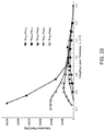
- FIG. 20 depicts a plot of saturation field as a function of coupling layer thickness, t c , for various magnetic structures fabricated with a coupling layer comprising Ru 100 ⁇ x Fe x or a coupling layer comprising fabricated with a coupling layer comprising Ru 100 ⁇ x Co x .
- FIG. 21 depicts a plot of coupling angle as a function of atomic concentration parameter, x, for various magnetic structures having different coupling layers.
- FIG. 22 depicts a plot of coupling angle as a function of coupling layer thickness, t c , for various magnetic structures having different coupling layers.
- FIG. 23 depicts a plot of coupling angle as a function of atomic concentration parameter, x, for various magnetic structures having different coupling layers.
- FIG. 24 depicts a plot bilinear coupling strength, J 1 , as a function of atomic concentration parameter, x, for various magnetic structures fabricated with coupling layers comprising Ru, Fe and Mn.
- FIG. 25 depicts a plot biquadratic coupling strength, J 2 , as a function of atomic concentration parameter, x, for various magnetic structures fabricated with coupling layers comprising Ru, Fe and Mn.
- FIG. 26 depicts a plot of saturation field as a function of atomic concentration parameter, x, for various magnetic structures fabricated with coupling layers comprising Ru, Fe and Mn.
- FIG. 27A schematically depicts a magnetic sensor according to a particular embodiment of the invention.
- FIG. 27B depicts a plot of coupling angle as a function of temperature for a temperature sensor according to a particular embodiment of the invention.
- FIG. 28 schematically depicts a magnetic memory device according a particular embodiment of the invention.
- FIG. 29 schematically depicts a magnetic memory device according another particular embodiment of the invention.
- FIGS. 30A, 30B and 30C schematically depict of oscillator devices according to particular embodiments of the invention.
- FIGS. 31A and 31B schematically depict an oscillator device combined with a memory device according to a particular embodiment of the invention in a first state and in a second state, respectively.
- One aspect of the invention provides a coupling layer for coupling magnetization directions (also referred to as magnetic moments) of two or more spaced apart magnetic layers.
- Other aspects of the invention provide a structure comprising two spaced apart magnetic layers and an interleaving coupling layer, wherein the magnetization directions of the magnetic layers are coupled to one another.
- Other aspects of the invention provide methods for fabricating such structures and/or methods for using such structures.
- Magnetization directions of magnetic layers may be ferromagnetically coupled such that, in the absence of an externally applied magnetic field, the magnetization directions (or magnetic moments) of the magnetic layers are aligned at (or substantially near) 0° with respect to one another.
- Magnetization directions of magnetic layers may be antiferromagnetically coupled such that, in the absence of an externally applied magnetic field, the magnetization directions (or magnetic moments) are aligned at (or substantially near) 180° with respect to one another.
- a reference angle e.g.
- substantially near may be understood to be ⁇ 5° from the reference angle. In some embodiments, substantially near may be ⁇ 2° from the reference angle. In some embodiments, substantially near may be ⁇ 1° from the reference angle.
- Magnetization directions of magnetic layers may be coupled such that, in the absence of an externally applied magnetic field, the magnetization directions (or magnetic moments) are aligned at a non-collinear angle ⁇ with respect to one another.
- non-collinear angles ⁇ may be greater than 0° and less than 180°, greater than 2° and less than 178°, greater than 5° and less than 175° or greater than 10° and less than 170°.
- Magnetization directions of magnetic layers may be coupled such that, in the absence of an externally applied magnetic field, the magnetization directions (or magnetic moments) are aligned at a non-orthogonal, non-collinear angle ⁇ with respect to one another.
- non-collinear angles ⁇ may be: greater than 0° and less than 90° or greater than 90° and less than 180°; greater than 2° and less than 88° or greater than 92° and less than 178°; greater than 5° and less than 85° or greater than 95° and less than 175°; or greater than 10° and less than 80° or greater than 100° and less than 170°.
- FIGS. 2A and 2B depict a magnetic structure 10 comprising a coupling layer 20 according to one aspect of the invention.
- Coupling layer 20 of FIG. 2A is interposed between and in contact with both of a first magnetic layer 30 and a second magnetic layer 40 , such that first and second magnetic layers 30 , 40 are spaced apart from one another in the Z direction (shown in FIGS. 2A and 2B ).
- First magnetic layer 30 has a first magnetization direction (or magnetic moment) 32 and second magnetic layer 40 has a second magnetization direction (or magnetic moment) 42 .
- First magnetic layer 30 of the illustrated embodiment comprises first and second first magnetic layer surfaces 36 , 38 which comprise opposing, generally planar surfaces 36 , 38 that each extend in the X and Y directions. Any spatial variation of first and second first magnetic layer surfaces 36 , 38 in the Z direction (e.g. due to the surfaces not being perfectly planar or smooth) may be considerably less (e.g. one or more orders of magnitude less) than the X and Y extents of first magnetic layer surfaces 36 , 38 .
- First generally planar first magnetic layer surface 36 may be separated from second generally planar first magnetic layer surface 38 by a thickness, t m1 , in the Z direction. In some embodiments, thickness, t m1 , is greater than approximately 0.2 nm.
- thickness, t m1 is greater than approximately 0.3 nm. In some embodiments, thickness, t m1 , is greater than approximately 0.5 nm. In some embodiments, thickness, t m1 , is greater than approximately 1.0 nm. In some embodiments, thickness, t m1 , is greater than approximately 1.5 nm. Thickness, t m1 , is not necessarily consistent across the entirety of first magnetic layer 30 and may vary due to, for example, imperfections in one or both of first and second first magnetic layer surfaces 36 , 38 .
- Second magnetic layer 40 of the illustrated embodiment comprises first and second second magnetic layer surfaces 46 , 48 which comprise opposing, generally planar surfaces 46 , 48 that each extend in the X and Y directions. Any spatial variation of first and second first magnetic layer surfaces 46 , 48 in the Z direction (e.g. due to the surfaces not being perfectly planar or smooth) may be considerably less (e.g. one or more orders of magnitude less) than the X and Y extents of second magnetic layer surfaces 46 , 48 .
- First generally planar second magnetic layer surface 46 may be separated from second generally planar second magnetic layer surface 48 by a thickness, t m2 , in the Z direction. In some embodiments, thickness, t m2 , is greater than approximately 0.2 nm.
- thickness, t m2 is greater than approximately 0.5 nm. In some embodiments, thickness, t m2 , is greater than approximately 1.0 nm. In some embodiments, thickness, t m2 , is greater than approximately 1.5 nm. Thickness, t m2 , is not necessarily consistent across the entirety of second magnetic layer 40 and may vary due to, for example, imperfections in one or both of first and second magnetic layer surfaces 46 , 48 .
- first and second magnetization directions 32 , 42 are in planes defined by the X and Y directions. This is not mandatory. One or both of first and second magnetization directions 32 , 42 could extend in any combination of the X, Y and Z directions.
- Coupling layer 20 is interposed between first and second magnetic layers 30 , 40 .
- Coupling layer 20 may comprise first and second coupling layer surfaces 26 , 28 which may comprise opposing, generally planar surfaces 26 , 28 that each extend in the X and Y directions. Any spatial variation of first and second coupling layer surfaces 26 , 28 in the Z direction (e.g. due to the surfaces not being perfectly planar or smooth) may be considerably less (e.g. one or more orders of magnitude less) than the X and Y extents of coupling layer surfaces 26 , 28 .
- First coupling layer surface 26 may be separated from second coupling layer surface 28 by a thickness, t c , in the Z direction.
- thickness, t c may be between 0.3 nm to 8.0 nm. In some embodiments, thickness, t c , may be between 0.3 nm to 2.5 nm. In some embodiments, thickness, t c , may be between 0.4 nm to 2.0 nm. In some embodiments, thickness, t c , may be between 0.6 nm to 2.0 nm. Thickness, t c , is not necessarily consistent across the entirety of coupling layer 20 and may vary due to, for example, imperfections in one or both of first and second coupling layer surfaces 26 , 28 .
- first generally planar first magnetic layer surface 36 abuts second generally planar coupling layer surface 28 and/or first generally planar coupling layer surface 26 abuts first generally planar second magnetic layer surface 46 .
- coupling layer 20 may be layered directly adjacent to first magnetic layer 30 and second magnetic layer 40 may be layered directly adjacent to coupling layer 20 .
- one or more of first magnetic layer 30 , second magnetic layer 40 and coupling layer 20 have different X-Y plane dimensions. This is not mandatory.
- magnetic layers 30 , 40 and/or coupling layer 20 need not have strictly planar surfaces. Layers 30 , 40 and/or 20 could conform to the shape of a non-planar substrate.
- magnetic layers 30 , 40 and/or coupling layer 20 shown in the views of FIGS. 2A and 2B may represent portions of non-illustrated magnetic layers and/or a coupling layer which is/are larger than the portions shown in the FIGS. 2A and 2B illustrations.
- First magnetic layer 30 may comprise any suitable magnetic layer.
- First magnetic layer 30 may exhibit a magnetization direction (magnetic moment) 32 .
- first magnetic layer 30 may comprise a ferromagnetic material such as, for example, one or more elements or alloys selected from a group consisting of Co, Fe, Ni and alloys thereof.
- First magnetic layer 30 may additionally or alternatively comprise Mn (although Mn is not, strictly speaking, ferromagnetic) and alloys thereof.
- Mn although Mn is not, strictly speaking, ferromagnetic
- Co, Ni and Fe have a ferromagnetic spin arrangement while Mn has antiferromagnetic spin arrangement.
- First magnetic layer 30 may additionally or alternatively comprise, for example, one or more elements or alloys selected from a group consisting of Co, Fe, Ni, and Mn and alloys thereof, and an additive element, said additive element being one or more elements selected from a group consisting of B, C, N, O, F, Mg, Al, Si, P, S, Sc, Ti, V, Cr, Mn, Cu, Zn, Ga, Ge, As, Se, Y, Zr, Nb, Mo, Tc, Ru, Rh, Pd, Ag, Cd, In, Sn, Sb, Te, La, Ce, Pr, Nd, Pm, Sm, Eu, Gd, Tb, Dy, Ho, Er, Tm, Yb, Lu, Hf, Ta, W, Re, Os, Ir, Pt, Au, Hg, TI, Pb, Bi and/or alloys thereof.
- additive element being one or more elements selected from a group consisting of B, C, N, O, F, Mg, Al, Si,
- first magnetic layer 30 additionally or alternatively comprises one of, for example, RuCo, RuFe, RuNi, RuCoFe, RuFeNi, RuCoNi, RuFeCoNi, FeCoB, FeCoNiSiB, FeCoZr, FeCoRu, CoCr, CoCrB, CoPt, FePt, Gd, Dy, MnAs, MnBi, MnSb, MnBiSi, MnBiSiAl, CrO 2 , ErO and GdFeCo.
- first magnetic layer 30 additionally or alternatively comprises an L 10 compound such as, for example, a combination of one or more of Co, Fe, Ni and one or more of Pt and Pd, FePtAg, FePtCu, and FePtCuAg, or an L 10 compound with an oxide or carbon.
- first magnetic layer 30 additionally or alternatively comprises CoPt. CoRu, CoRh, CoCr with or without an oxide.
- first magnetic layer 30 additionally or alternatively comprises one or more Heusler compounds in the form Co 2 ab, where a is at least one element from the group consisting of Mn, Fe and Cr, and b is at least one element from the group consisting of Si, Ge and Al,
- first magnetic layer 30 additionally or alternatively comprises a composite layer made up of a plurality of individual sub-layers, wherein each sub-layer may have the same or a different composition.
- first magnetic layer 30 may comprise a first sub-layer of FeCoB and a second sub-layer of CoFe.
- the material of first magnetic layer 30 is chosen based at least in part on the material of coupling layer 20 .
- magnetic layer 30 may be chosen to allow inter-diffusion between magnetic layer 30 and coupling layer 20 .
- Second magnetic layer 40 may comprise any suitable magnetic layer, and may be fabricated to exhibit any of the properties and/or characteristics and/or may comprise the same materials as discussed herein for first magnetic layer 30 .
- Second magnetic layer 40 may have a magnetization direction (magnetic moment) 42 .
- second magnetic layer 40 is substantially similar to first magnetic layer 30 .
- second magnetic layer 40 is different than first magnetic layer 30 .
- first and second magnetic layers 30 , 40 may differ in composition to thereby induce different structural and/or magnetic properties such as, but not limited to, structure, saturation magnetization, anisotropy, cure temperature, exchange stiffness, and/or damping.
- First and second magnetic layers 30 , 40 may also differ in size and/or shape.
- t m1 may be different than t m2 or the X and/or Y dimensions of first magnetic layer 30 may be different from those of coupling layer 20 and/or second magnetic layer 40 .
- Coupling layer 20 may comprise at least one first group element 22 and at least one second group element 24 .
- the second group element 24 may be referred to herein as a dopant.
- the first group elements 22 may comprise non-magnetic elements while the second group elements 24 may comprise magnetic elements. Consequently, the first group elements 22 may also be referred to herein as the non-magnetic group elements 22 and the second group elements 24 may be referred to herein as the magnetic group elements 24 .
- the at least one first (non-magnetic) group element 22 may comprise or be selected from the group consisting of Ag, Cr, Ru, Mo, Ir, Rh, Cu, V, Nb, W, Ta, Ti, Re, Os, Au, Al and Si.
- each element in this group of non-magnetic elements is known to exhibit at least some antiferromagnetic coupling when the element is used alone (purely or almost purely) as a coupling layer between a pair of magnetic layers and, consequently, the inventors have strong reason to believe that each of the elements in this group can exhibit strong antiferromagnetic coupling or non-collinear coupling when suitably doped with at least one second (magnetic) group element 22 as discussed herein.
- the at least one first (non-magnetic) group element may comprise or be selected from the sub-group consisting of Cr, Ru, Rh, Re, Ir.
- Each of the non-magnetic elements in this sub-group is known to exhibit particularly strong antiferromagnetic coupling when the element is used alone (purely or almost purely) as a coupling layer between a pair of magnetic layers and, consequently, the inventors have strong reason to believe that each of the elements in this sub-group can exhibit strong antiferromagnetic coupling or non-collinear coupling when suitably doped with at least one second (magnetic) group element 22 as discussed herein.
- the at least one first (non-magnetic) group element may comprise or be selected from the further sub-group consisting of Ru, Ir, and Rh.
- each of the non-magnetic elements in this further sub-group is known to exhibit even greater antiferromagnetic coupling when the element is used alone (purely or almost purely) as a coupling layer between a pair of magnetic layers and, consequently, the inventors have strong reason to believe that each of the elements in this further sub-group can exhibit strong antiferromagnetic coupling or non-collinear coupling when suitably doped with at least one second (magnetic) group element 22 as discussed herein.
- the at least one first (non-magnetic) group element comprises or consists of Ru.
- the at least one second (magnetic) group element 24 may comprise or be selected from the group consisting of ferromagnetic elements Ni, Co and Fe.
- the at least one second (magnetic) group element 24 may additionally or alternatively comprise or be selected from the group consisting of magnetic elements Mn, Ni, Co and Fe.
- the at least one second (magnetic) group element 24 may additionally comprise a polarizable element selected from the group of Pd and Pt.
- Such polarizable elements could, in some embodiments, be substituted for a portion of the second (magnetic) group elements 24 .
- Pd or Pt may be substituted one atom for every atom of second group (magnetic) element 24 although this is not mandatory.
- up to 90% of the second (magnetic) group elements 24 may be substituted by Pd or Pt or a combination of Pd and Pt.
- Mn may be substituted for a portion of second (magnetic) group elements 24 .
- Mn may be referred to herein as a magnetic element, magnetic atom or magnetic material where it is sought to include Mn with ferromagnetic elements Co, Ni and Fe, but ferromagnetic elements should be considered to exclude Mn.
- the atomic concentration ratio of the at least one first (non-magnetic) group element 22 to the at least one second (magnetic) group element 24 within coupling layer 20 may be (100 ⁇ x):x, where x>0. It should be understood that the atomic concentration ratio of the at least one first (non-magnetic) group element 22 to the at least one second (magnetic) group element 24 within coupling layer 20 is an aggregate atomic concentration ratio that accounts for the composition of the entire coupling layer 20 .
- Coupling layer 20 may be relatively homogenous throughout, such that the atomic concentration ratio is generally consistent throughout coupling layer 20 or coupling layer 20 may include regions or portions in which the atomic concentration ratio is higher or lower than the aggregate atomic concentration ratio.
- coupling layer 20 may be fabricated in sub-layers, each sub-layer having an individual atomic concentration ratio of the at least one first (non-magnetic) group element 22 to the at least one second (magnetic) group element 24 wherein the aggregate of the individual atomic concentration ratios (over coupling layer 20 ) is (100 ⁇ x):x, where x>0.
- the at least one first (non-magnetic) group element 22 and the at least one second (magnetic) group element 24 and/or the atomic concentration parameter x in the atomic concentration ratio of the at least one first (non-magnetic) group element 22 to the at least one second (magnetic) group element 24 may be chosen such that first and second magnetization directions 32 , 42 of first and second magnetic layers 30 , 40 are coupled at a non-collinear angle ⁇ with respect to one another in the absence of an externally applied magnetic field in which case structure 10 , its magnetic layers 30 , 40 and/or its magnetization directions 32 , 42 may be said to be non-collinearly coupled.
- the at least one first (non-magnetic) group element 22 and the at least one second (magnetic) group element 24 and/or the atomic concentration parameter x in the atomic concentration ratio of the at least one first (non-magnetic) group element 22 to the at least one second (magnetic) group element 24 may be chosen such that first and second magnetization directions 32 , 42 of first and second magnetic layers 30 , 40 are coupled at a non-orthogonal and non-collinear angle ⁇ with respect to one another in the absence of an externally applied magnetic field—in which case structure 10 , its magnetic layers 30 , 40 and/or its magnetization directions 32 , 42 may be said to be non-orthogonally and non-collinearly coupled.
- the at least one first (non-magnetic) group element 22 , the at least one second (magnetic) group element 24 and/or the atomic concentration parameter x may be chosen such that the biquadratic magnetic coupling strength J 2 of coupling layer 20 is greater than or equal to half of the absolute value of the bilinear magnetic coupling strength J 1 of coupling layer 20 .
- the coupling layer thickness t c may also be chosen to create non-collinear and/or non-orthogonal/non-collinear coupling between magnetic layers 30 , 04 of structure 10 .
- the at least one first (non-magnetic) group element 22 , the at least one second (magnetic) group element 24 , the thickness of coupling layer 20 (t c ) and/or the atomic concentration parameter x may be chosen based at least in part on the composition of first and second magnetic layers 30 , 40 .
- the at least one first (non-magnetic) group element 22 , the at least one second (magnetic) group element 24 , the thickness of coupling layer 20 (t c ) and/or the atomic concentration parameter x may be chosen based at least in part on the thickness of one or both of first and second magnetic layers 30 , 40 (e.g. t m1 , t m2 ).
- the at least one first (non-magnetic) group element 22 , the at least one second (magnetic) group element 24 , the thickness of coupling layer 20 (t c ) and/or the atomic concentration parameter x may be chosen such that the saturation field of structure 10 is greater than 1,000 Oe, 3,000 Oe, 20,000 Oe or 50,000 Oe.
- Such high saturation field structures may be non-collinearly coupled, non-orthogonally and non-collinearly coupled or antiferromagnetically coupled.
- the at least one first (non-magnetic) group element 22 , the at least one second (magnetic) group element 24 , the thickness of coupling layer 20 (t c ) and/or the atomic concentration parameter x may be chosen such that the biquadratic coupling strength, J 2 , of structure 10 is greater than 0.1 mJ/m 2 , 0.2 mJ/m 2 , 0.5 mJ/m 2 , 1.0 mJ/m 2 , 1.5 mJ/m 2 , or even 2.0 mJ/m 2 and J 2 is greater than half of the absolute value of J 1 .
- Such high coupling strength structures may be non-collinearly coupled, non-orthogonally and non-collinearly coupled or antiferromagnetically coupled.
- the at least one first (non-magnetic) group element 22 , the at least one second (magnetic) group element 24 , the thickness of coupling layer 20 (t c ) and/or the atomic concentration parameter x may be chosen such that magnetic structure 10 may withstand annealing at a temperature of 100° C. or higher, 150° C. or higher, or 200° C. or higher without undesirably changing the coupling angle of first and second magnetic layers, 30 , 40 .
- Such annealable structures may be non-collinearly coupled, non-orthogonally and non-collinearly coupled or antiferromagnetically coupled.
- it may be desirable for the coupling angle of first and second magnetic layers 30 , 40 to change with annealing and the at least one first (non-magnetic) group element 22 , the at least one second (magnetic) group element 24 , the thickness of coupling layer 20 (t c ) and/or the atomic concentration parameter x may be chosen such that the coupling angle may be controllably changed as desired by annealing at a temperature of 100° C. or higher, 150° C. or higher or 200° C. or higher.
- coupling layer 20 may comprise at least one first group element 22 and at least two second group elements 24 .
- the first group elements 22 may comprise non-magnetic elements while the second group elements 24 may comprise magnetic elements.
- the at least one first (non-magnetic) group element 22 may comprise or be selected from the group consisting of Ag, Cr, Ru, Mo, Ir, Rh, Cu, V, Nb, W, Ta, Ti, Re, Os, Au, Al and Si.
- the at least one first (non-magnetic) group element may comprise or be selected from the group consisting of Ru, Ir, Re, Rh, and Cr.
- the at least one first (non-magnetic) group element comprises or consists of Ru.
- the at least two second (magnetic) group elements comprise Co and Fe.
- the atomic concentration ratio of the first magnetic group element (e.g. Co) to the second magnetic group element (e.g. Fe) may be any suitable ratio. As the ratio of the first magnetic group element to the second magnetic group element increases, coupling layer 20 may behave more like a coupling layer of the nonmagnetic element 24 (e.g. Ru) and the first magnetic group element (e.g. Co) while as the ratio of the first magnetic group element to the second magnetic group element decreases, coupling layer 20 may behave more like a coupling layer of the nonmagnetic element 24 (e.g. Ru) and the second magnetic group element (e.g. Fe).
- the nonmagnetic element 24 e.g. Ru
- the second magnetic group element e.g. Fe
- coupling layer 20 may behave more like a RuCo coupling layer 20 and as the ratio of Co to Fe decreases, coupling layer 20 may behave more like a RuFe coupling layer 20 .
- the properties of a coupling layer 20 that comprises at least one first group element 22 and at least two magnetic group elements 24 may therefore be estimated or predicted by observing the properties of two coupling layers 20 each having only one of the at least two magnetic group elements 24 in combination with the at least on first group element 22 and based on the ratio of the first magnetic group element to the second magnetic group element.
- coupling layer 20 may comprise at least two first group elements 22 and at least one second group element 24 .
- the at least two first group elements 22 may comprise Ru and at least one second non-magnetic element comprising or selected from the group consisting of: Ag, Cr, Mo, Ir, Rh, Cu, V, Nb, W, Ta, Ti, Re, Os, Au, Al and Si.
- the at least one second group element 24 may comprise at least one magnetic element comprising or selected from the group consisting of: Ni, Co and Fe.
- the atomic ratio of the at least one first non-magnetic element to the at least one second non-magnetic element to the at least one magnetic element is (100 ⁇ x ⁇ y):y:x. In some embodiments, y is less than 80.
- the at least one second non-magnetic element is selected from the group consisting of Ru, Ir, Re, Rh, and Cr.
- the at least one first (non-magnetic) group element 22 and the at least one second (magnetic) group element 24 and/or the atomic concentration parameter x in the atomic concentration ratio of the at least one first (non-magnetic) group element 22 to the at least one second (magnetic) group element 24 may be chosen such that first and second magnetization directions 32 , 42 of first and second magnetic layers 30 , 40 are coupled at an antiferromagnetic angle with respect to one another in the absence of an externally applied magnetic field in which case structure 10 , its magnetic layers 30 , 40 and/or its magnetization directions 32 , 42 may be said to be antiferromagnetically coupled.
- antiferromagnetic angles may be: greater than 170° and less than 190° or greater than 175° and less than 185°; greater than 178° and less than 182°; greater than 179° and less than 181°; greater than 179.5° and less than 180.5°; or even 180°.
- the at least one first (non-magnetic) group element 22 , the at least one second (magnetic) group element 24 , the thickness of coupling layer 20 (t c ) and/or the atomic concentration parameter x may be chosen based at least in part on the composition of first and second magnetic layers 30 , 40 .
- the at least one first (non-magnetic) group element 22 , the at least one second (magnetic) group element 24 , the thickness of coupling layer 20 (t c ) and/or the atomic concentration parameter x may be chosen based at least in part on the thickness of one or both of first and second magnetic layers 30 , 40 (e.g. t m1 , t m2 ).
- the at least one first (non-magnetic) group element 22 , the at least one second (magnetic) group element 24 , the thickness of coupling layer 20 (t c ) and/or the atomic concentration parameter x may be chosen such that the saturation field of structure 10 is greater than 1,000 Oe, 3,000 Oe, 20,000 Oe or 50,000 Oe.
- the at least one first (non-magnetic) group element 22 , the at least one second (magnetic) group element 24 , the thickness of coupling layer 20 (t c ) and/or the atomic concentration parameter x may be chosen such that the bilinear coupling strength, J 1 is greater than 0.3 mJ/m 2 , 0.6 mJ/m 2 0.8 mJ/m 2 and/or the biquadratic coupling strength, J 2 , of structure 10 is greater than 0.1 mJ/m 2 , 0.2 mJ/m 2 , 0.5 mJ/m 2 , 1.0 mJ/m 2 , 1.5 mJ/m 2 , or even 2.0 mJ/m 2 and J 2 is greater less than half of the absolute value of J 1 .
- the at least one first (non-magnetic) group element 22 , the at least one second (magnetic) group element 24 , the thickness of coupling layer 20 (t c ) and/or the atomic concentration parameter x may be chosen such that magnetic structure 10 may withstand annealing at a temperature of 100° C. or higher, 150° C. or higher, or 200° C. or higher without undesirably changing the coupling angle of first and second magnetic layers, 30 , 40 .
- the coupling angle of first and second magnetic layers 30 , 40 may be desirable for the coupling angle of first and second magnetic layers 30 , 40 to change with annealing and the at least one first (non-magnetic) group element 22 , the at least one second (magnetic) group element 24 , the thickness of coupling layer 20 (t c ) and/or the atomic concentration parameter x may be chosen such that the coupling angle may be controllably changed as desired by annealing at a temperature of 100° C. or higher, 150° C. or higher or 200° C. or higher.
- the at least one first (non-magnetic) group element 22 comprises Ru or alloys thereof and the at least one second (magnetic) group element 24 comprises Fe or alloys thereof.
- the at least one first (non-magnetic) group element 22 comprises one or more of Cr, Ir, Rh and Re or alloys thereof and the at least one second (magnetic) group element 24 comprises one or more of Fe, Ni and Co or alloys thereof.
- the at least one first (non-magnetic) element 22 comprises Ru and at least one second non-magnetic element selected from the group consisting of: Ag, Cr, Mo, Ir, Rh, Cu, V, Nb, W, Ta, Ti, Re, Os, Au, Al and Si and the at least one magnetic element comprises or is selected from the group consisting of: Ni, Co and Fe.
- first and second magnetic layers 30 , 40 comprise at least one of Co, Ni or alloys thereof.
- the at least one second (magnetic) group element 24 may additionally comprise a polarizable element selected from the group of Pd and Pt.
- Such polarizable elements could, in some embodiments, be substituted for a portion of the second (magnetic) group elements 24 .
- Pd or Pt may be substituted one atom for every atom of second group (magnetic) element 24 although this is not mandatory.
- up to 90% of the second (magnetic) group elements 24 may be substituted by Pd or Pt or a combination of Pd and Pt.
- Mn may be substituted for a portion of second (magnetic) group elements 24 .
- first and second magnetization directions 32 , 42 may point in any direction in space and may not be limited to any particular plane(s). It follows that for a given first magnetization direction 32 , second magnetization direction 42 may point in an infinite number of directions while first and second magnetization directions 32 , 43 are non-collinearly coupled to one another. This description may use the symbol ⁇ to refer to the angle ⁇ between first and second magnetization directions 32 , 42 .
- FIG. 3 schematically depicts a first magnetization direction 32 and a number of exemplary non-collinearly coupled second magnetization directions 42 from among the infinite number of possible non-collinearly coupled second magnetization directions 42 which could be implemented in structure 10 .
- First magnetization direction 32 may be coupled to second magnetization direction 42 due to the presence of coupling layer 20 .
- the strength or energy of the coupling between magnetic moments 32 , 42 of first magnetic layer 30 and second magnetic layer 40 across coupling layer 20 in magnetic structure 10 may be characterized using a bilinear coupling strength parameter, J 1 and biquadratic coupling strength parameter, J 2 .
- J 1 and J 2 represent parameters of a model which relates the dependence of total magnetization of structure 10 in the direction of an externally applied magnetic field to a strength of the externally applied magnetic field.
- the J 1 and J 2 parameters of structure 10 may be experimentally ascertained by applying external magnetic field to structure 10 , measuring the magnetization and selecting J 1 and J 2 to best fit the model to the experimental results.
- the model may assume magnetic moments 32 , 42 in first magnetic layer 30 and second magnetic layer 40 are parallel to the film plane (i.e. in a direction that is a linear combination of the X and Y directions shown in FIG. 2A ).
- the model may further assume that both first magnetic layer 30 and second magnetic layer 40 consist of one or more magnetic sublayers interacting through the direct exchange interaction as proposed by C. Eyrich et. al., PHYSICAL REVIEW B, 90, 235408 (2014), which is hereby incorporated herein by reference.
- antiferromagnetic, ferromagnetic and non-collinear coupling are dependent on the relationships between bilinear, J 1 , biquadratic, J 2 , and higher order coupling parameters.
- the bilinear coupling parameter, J 1 dominates the other coupling parameter (e.g. the absolute value of J 1 is greater than half of the sum of the absolute values of the other coupling parameters) and J 1 is less than zero, the resulting coupling is ferromagnetic.
- the bilinear coupling parameter, J 1 dominates the other coupling parameter (e.g.
- the absolute value of J 1 is greater than half of the sum of the absolute values of the other coupling parameters) and J 1 is greater than zero, the resulting coupling is antiferromagnetic. It is further believed that if the biquadratic coupling parameter, J 2 , dominates (e.g. is greater than half of the sum of the other coupling parameters) and J 1 is small, the magnetic moments 32 , 42 of first magnetic layer 30 and second magnetic layer 40 may be aligned at a non-collinear angle ⁇ between approximately 80° to 100°, in some embodiments, at 90°, or, in some embodiments, substantially near 90°.
- a mixture of the bilinear and biquadratic parameters, J 1 , J 2 can result in non-collinear coupling such that the magnetic moments 32 , 42 of first magnetic layer 30 and second magnetic layer 40 are aligned at a non-collinear angle ⁇ which may, in some embodiments, be greater than 0° and less than 180°, in some embodiments, between 1° and 179°, in some embodiments, between 5° and 175° or, in some embodiments, between 20° and 160°.
- the bilinear coupling parameter, J 1 can either be positive or negative, and the biquadratic, J 2 , coupling parameter has a positive value. Both parameters vary in magnitude/strength.
- FIG. 4 depicts a plot of the equation (1) coupling energy versus angle ⁇ with four different relationships of the magnitudes of J 1 to J 2 .
- J 2 is increased to just greater than half of J 1 (as represented by the thin solid line in FIG. 4 )
- J 2 1 ⁇ 2
- J 1 is negative (not depicted)
- a magnetic structure (such as magnetic structure 10 ) may be fabricated by layering on top of a seed layer (also referred to herein as an underlayer).
- a seed layer also referred to herein as an underlayer.
- FIG. 5 depicts a magnetic structure 10 ′, substantially similar to magnetic structure 10 , layered on a seed layer 50 .
- Seed layer 50 may comprise any suitable seed layer, as is known in the art.
- seed layer 50 may comprise at least one element selected from the group comprising or consisting of B, C, Si, Ge, Al, Ti, V, Cr, Mn, Fe, Co, Ni, Cu, Zr, Nb, Mo, Ru, Rh, Pd, Ag, Hf, Ta, W, Re, Ir, Pt, and Au.
- seed layer 50 may comprise a first sub-layer comprising at least one element comprising or selected from the group consisting of: B, Si, Ge, Al, Ti, V, Cr, Mn, Fe, Co, Ni, Cu, Zr, Nb, Mo, Ru, Rh, Pd, Ag, Hf, Ta, W, Re, Ir, Pt, and Au and a second layer comprising at least one element comprising or selected from the group consisting of N, and O.
- Seed layer 50 may be used in the fabrication of magnetic structure 10 ′ for one or more of the following reasons: to ease fabrication or for protection of first magnetic layer 30 , to set a growth of magnetic layer 30 along a preferred crystallographic orientation, to serve as an electrical contact, to serve as a protective layer, to maximize the surface anisotropy at the interface between seed layer 50 and first magnetic layer 30 , and/or to control thermal conductivity.
- a protective layer may be layered on second magnetic layer 40 .
- protective layer 55 is layered on second magnetic layer 40 to protect second magnetic layer 40 from, for example, oxidation, corrosion, physical wear etc.
- Protective layer 55 may serve as an electrical contact or part of an electrical contact.
- Protective layer 55 may comprise any suitable material.
- protective layer 55 may comprise at least one element comprising or selected from the group consisting of Al, Ti, V, Cr, Mn, Fe, Co, Ni, Cu, Zr, Nb, Mo, Ru, Rh, Pd, Ag, Hf, Ta, W, Re, Ir, Pt, and Au.
- protective layer 55 may additionally or alternatively comprise nitrides such Si—N, Ti—N or oxides such as Ti—O, Al—O, Si—O.
- magnetic layers 30 , 40 and coupling layer 20 of magnetic structure 10 ′ may be substantially similar to magnetic structure 10 and may comprise any of the features of magnetic structure 10 described herein.
- magnetic structure 10 may be fabricated to comprise a seed layer 50 and/or a protective layer 55 .
- Magnetic structure 10 may be fabricated using any suitable technique.
- structure 10 is fabricated by, for example, physical vapor deposition (e.g. sputtering), atomic layer deposition, or chemical vapor deposition.
- magnetic structure 10 may be fabricated using sputtering, whereby particles are ejected from a solid target material due to bombardment of the target by energetic particles such as gas ions, as is known in the art.
- FIG. 6A depicts a first step of layering a first magnetic layer 30 on a seed layer (also referred to as an underlayer or substrate) 50 .
- This first step may be accomplished by sputtering, such as is depicted in FIG. 6A .
- a target 39 of the same material as is desired for first magnetic layer 30 may be bombarded by energized particles (not shown), such that particles 39 A of target material 39 are deposited on seed layer 50 to create first magnetic layer 30 .
- first magnetic layer 30 may comprise a plurality of elements deposited from a single target 39 (e.g.
- target 39 may be prefabricated to have the desired constituent elements as is desired for magnetic layer 30 ) or may comprise a plurality of materials (e.g. elements) deposited from multiple targets 39 , each target optionally comprising a different material.
- the thickness, t m1 , of first magnetic layer 30 increases until a desired thickness, t m1 , is achieved.
- surface 36 of first magnetic layer 30 may not be perfectly planar due to the distribution of particles 39 A.
- FIG. 6B depicts a second step of layering coupling layer 20 on first magnetic layer 30 .
- This second step may be accomplished by sputtering.
- a target 29 of the same constituent materials as is desired for coupling layer 20 may be bombarded by energized particles (not shown), such that particles 29 A of target material 29 are deposited on first magnetic layer 30 to create coupling layer 20 .
- coupling layer 20 may comprise a plurality of elements deposited from a single target 29 (e.g. where the target 29 may be prefabricated to have the desired constituent elements for coupling layer 20 ).
- Such constituent elements which may be pre-fabricated into target 29 may comprise the at least one first (non-magnetic) group element 22 and the at least one second (magnetic) group element 24 .
- coupling layer 20 may be fabricated from a plurality of materials (e.g. elements) deposited from multiple targets 29 , each target 29 optionally comprising a different material.
- One of such multiple targets 29 may comprise the at least one first (non-magnetic) group element 22 and another one of such multiple targets 29 may comprise the at least one second (magnetic) group element 24 .
- the atomic concentration parameter x may be controlled, for example, by controlling the relative power of the energized particles that are used to bombard the various targets 29 .
- the thickness, t c of coupling layer 20 grows until a desired thickness, t c , is achieved.
- the interface between surface 28 of coupling layer 20 and surface 36 of first magnetic layer 30 may not be perfectly planar due to the distribution of particles 29 A and 39 A.
- surface 26 of coupling layer 20 may not be perfectly planar due to the distribution of particles 29 A.
- FIG. 6C depicts a third step of layering a second magnetic layer 40 on coupling layer 20 .
- This third step may be accomplished by sputtering, such as is depicted in FIG. 6C .
- a target 49 of the same material as is desired for second magnetic layer 40 may be bombarded by energized particles such that particles 49 A of target material 49 are deposited on coupling layer 20 to create second magnetic layer 40 .
- target 49 is the same as target 39 and magnetic layers 30 , 40 are made of the same material.
- targets 39 and 49 may comprise different materials such that first and second magnetic layers 30 , 40 may comprise different materials.
- second magnetic layer 40 may comprise a plurality of elements deposited from a single target 49 (e.g. where the target 49 may be prefabricated to have the desired constituent elements for magnetic layer 40 ) or may comprise a plurality of materials (e.g. elements) deposited from multiple targets 49 , each target 49 optionally comprising a different material.
- particles 49 A of target material 49 are deposited on coupling layer 20 , the thickness, t m2 , of second magnetic layer 40 grows until a desired thickness, t m2 , is achieved. As can be seen from FIG.
- the interface between surface 26 of coupling layer 20 and surface 46 of second magnetic layer 40 may not be perfectly planar due to the distribution of particles 29 A and 39 A. Further, surface 48 of second magnetic layer 40 may not be perfectly planar due to the distribution of particles 49 A.
- protective layer 55 may be layered on top of second magnetic layer 40 to protect the magnetic structure.
- a layer of Ru may be layered on top of second magnetic layer 40 using sputtering or any other suitable technique.
- the sputtering process occurs in a single chamber that contains targets 29 , 39 , 49 . In other embodiments, separate chambers are employed for sputtering one or more of targets 29 , 39 , 49 .
- a coupling layer 20 may be fabricated to comprise a compound made of at least one first (non-magnetic) group element 22 and at least one second (magnetic) group element 24 in whole or in part through annealing.
- a coupling layer 20 comprising a first (non-magnetic) group element 22 may be layered between first and second magnetic layers 30 , 40 , where each of the first and second magnetic layers 30 , 40 comprise at least one element from second (magnetic) group 24 to form an initial structure.
- This initial structure may be fabricated using, for example, sputtering as explained above in connection with FIG. 6 .
- the initial structure 10 may then be annealed.
- second (magnetic) group element 22 atoms from magnetic layers 30 , 40 may diffuse from first and second magnetic layers 30 , 40 into coupling layer 20 , such that the composition of coupling layer 20 will change from comprising at least one first (non-magnetic) group element 22 to comprising at least one element of first (non-magnetic) group 22 and at least one element from second (magnetic) group 24 .
- annealing may be employed to modify the concentration of second (magnetic) group element 24 within a coupling layer 20 that already comprises elements from both first (non-magnetic) group 22 and second (magnetic) group 24 .
- FIG. 7 schematically depicts this annealing-based process to fabricate a magnetic structure 10 .
- first and second magnetic layers 30 , 40 are fabricated (e.g. by sputtering) from a second (magnetic) group element (e.g. Co) and an initial coupling layer 20 ′ is fabricated (e.g. by sputtering) a first (non-magnetic) group (e.g. Ru).
- a first (non-magnetic) group e.g. Ru
- final coupling layer 20 comprising both first (non-magnetic) and second (magnetic) group elements.
- first (non-magnetic) and second (magnetic) group elements In addition to magnetic atoms from magnetic layers 30 , 40 diffusing into initial coupling layer 20 ′, some non-magnetic atoms from initial coupling layer 20 ′ may diffuse into magnetic layers 30 , 40 . Accordingly, final coupling layer 20 may be thicker than initial coupling layer 20 ′.
- the initial structure comprises an initial coupling layer 20 ′ comprising a first (non-magnetic) group element 22 and a second (magnetic) group element 24 in an atomic ratio of (100 ⁇ y):y.
- final coupling layer comprises an atomic ratio of first group element 22 to second group element 24 of (100 ⁇ x):x.
- y is equal to 0.
- y is greater than 0.
- y is less than x.
- the atomic concentration parameter, x may be greater than y due to diffusion of second group elements 24 into coupling layer 20 from magnetic layers 30 , 40 as discussed above. Accordingly, annealing may be employed to raise the concentration of second group element 24 in coupling layer 20 during fabrication to obtain a desired atomic concentration ratio of a first group element 22 to a second group element 24 .
- annealing comprises heating at least a portion of the magnetic structure to over 50° C. during at least a portion of fabrication. In some embodiments annealing comprises heating at least a portion of the magnetic structure to over 100° C. during at least a portion of fabrication. In some embodiments annealing comprises heating at least a portion of the magnetic structure to over 150° C. during at least a portion of fabrication. In some embodiments annealing comprises heating at least a portion of the magnetic structure to over 200° C. during at least a portion of fabrication. In some embodiments annealing comprises heating at least a portion of the magnetic structure to over 300° C. during at least a portion of fabrication.
- magnetic structure 10 is heated during at least a portion of fabrication (e.g. during physical vapor deposition, atomic layer deposition, or chemical vapor deposition of one or more of first magnetic layer 30 , coupling layer 20 and second magnetic layer 40 ). In some embodiments, magnetic structure is heated to over 100° C. during at least a portion of fabrication. In some embodiments, magnetic structure is heated to over 150° C. during at least a portion of fabrication. In some embodiments, magnetic structure is heated to over 200° C. during at least a portion of fabrication. In some embodiments, magnetic structure is heated to over 300° C. during at least a portion of fabrication. Heating during fabrication may encourage diffusion between one or more of first and second magnetic layers 30 , 40 and coupling layer 20 and may have a similar effect as annealing. Heating may be employed to achieve a desired atomic concentration parameter for coupling layer 20 .
- coupling layer 20 comprises Ru as a first (non-magnetic) group element 22 and Co as a second (magnetic) group element, and first and second magnetic layers 30 , 40 each comprise Co.
- Seed layer 50 may comprise Ta and Ru and protective layer 55 may comprise Ru.
- First and second magnetic layers 30 , 40 may each have a thickness of about 2.0 nm.
- Coupling layer 20 may comprise additional elements without substantively affecting operation of magnetic structure 10 .
- First and second magnetic layers 30 , 40 may also comprise additional elements without substantively affecting operation of magnetic structure 10 .
- the additional elements in magnetic layers 30 , 40 and coupling layer 20 may be ignored.
- Coupling layer 20 may have ratio of atomic concentration of Ru to Co of (100 ⁇ x):x, where x>0.
- the RuCo Embodiment coupling layer may be referred to as Ru 100 ⁇ x Co x .
- a similar naming convention may be used herein for other compositions.
- a coupling layer having a ratio of atomic concentration of Ru to Fe of (100 ⁇ x):x, where x>0, may be referred to as Ru 100 ⁇ x Fe x .
- the RuCo Embodiment magnetic structure 10 may be described using the following shorthand: Co(t m1 )/Ru 100 ⁇ x Co x (t c )/Co(t m2 ). This shorthand notation may also be used for other magnetic structures 10 , described herein.
- Ni(t m1 )/Ru 100 ⁇ x Fe x (0.75 nm)/Ni(t m2 ) refers to a magnetic structure having first and second magnetic layers 30 , 40 of Ni and a coupling layer 20 of Ru 100 ⁇ x Fe x having a thickness, t c , of 0.75 nm.
- FIG. 8 is a plot depicting the dependence of bilinear coupling strength J 1 between first and second magnetic layers 30 , 40 of a number of exemplary magnetic structures 10 fabricated in accordance with the RuCo Embodiment as a function of the thickness t c of coupling layer 20 for various values of x between 0 and 61.2 (e.g. where the atomic concentration ratio of Ru to Co is between 100:0 and 38:61.2).
- bilinear coupling strength J 1 of these magnetic structures is dependent on the atomic concentration ratio of Co to Ru in coupling layer 20 as well as the thickness, t c , of coupling layer 20 .
- FIG. 9 is a plot depicting the dependence of biquadratic coupling strength J 2 of the between first and second magnetic layers 30 , 40 of the same exemplary magnetic structures depicted in FIG. 8 as a function of the thickness t c of coupling layer 20 for various values of x between 0 and 61.2.
- biquadratic coupling strength J 2 of the RuCo Embodiment is dependent on the atomic concentration ratio of Co to Ru in coupling layer 20 as well as the thickness, t c , of coupling layer 20 .
- a coupling layer 20 having a thickness of approximately 0.6 nm may exhibit strong antiferromagnetic coupling, as compared to a pure Ru coupling layer 20 having a thickness of approximately 0.6 nm.
- FIG. 8 shows that the slope of bilinear coupling strength, J 1 , as it trends from positive to negative (e.g. the transition from antiferromagnetic to ferromagnetic coupling) as thickness, t c , decreases becomes less dramatic for x ⁇ 44.2 in coupling layer 20 (as shown by the gradual smooth curves for x ⁇ 44.2 in coupling layer 20 ).
- the region over which J 1 is trending to zero as thickness, t c decreases, (not shown in FIG. 8 ) is known to occur between 0.32 and 0.38 nm.
- the concentration of Co in Ru is increased, the region over which J 1 is trends to zero (has a positive slope in FIG.
- adding Co to Ru may result in an increase of the biquadratic coupling strength, J 2 for certain values of thickness t c of coupling layer 20 .
- a small biquadratic coupling strength, J 2 is observed.
- This relative size of the biquadratic coupling strength, J 2 is shown generally to increase with x and also to increase with a decrease in t c .
- biquadratic coupling strength, J 2 allows for non-collinear coupling, which, as discussed above, occurs when the biquadratic coupling strength, J 2 , is large in comparison to the bilinear coupling strength, J 1 .
- non-collinear coupling may occur when J 2 ⁇ 1 ⁇ 2
- FIG. 10 is a plot depicting the dependence of the coupling angle ⁇ between first and second magnetic layers 30 , 40 in a number of exemplary magnetic structures fabricated in accordance with the RuCo Embodiment as a function of the thickness t c of coupling layer 20 for various values of x between 0 and 63.6.
- non-collinear coupling can be achieved with x ⁇ 36.8 at various values of thickness t c of coupling layer 20 .
- non-collinear coupling at non-collinear angles ⁇ is observed at a coupling layer 20 thickness t c of between approximately 0.4 nm and 0.55 nm. If x is increased to 50.4, non-collinear coupling at angles between 100° and 180° is observed at a thickness t c of coupling layer 20 of between approximately 0.5 nm and 0.65 nm. If x is increased to 55.3, non-collinear coupling at angles between approximately 30° and 180° is observed at a thickness t c of coupling layer 20 of between approximately 0.45 nm and 0.9 nm.
- the rate of change of the non-collinear coupling angle ⁇ with respect to thickness t c of coupling layer 20 decreases as the concentration of Co (i.e. x) increases. Accordingly, as x increases, non-collinear coupling may be achieved over a greater range of thickness, t c .
- the relationship of the non-collinear coupling angle ⁇ with respect to thickness t c of coupling layer 20 is at least approximately linear above 0.4 nm.
- the coupling angle ⁇ is relatively constant (lower slope) in an angular range near 85° to 95° for values of coupling layer 20 thickness t c between 0.9 nm to 1.0 nm.
- the coupling angle ⁇ is also relatively constant near 130° for values of coupling layer 20 thickness t c between 1.1 nm to 1.2 nm. Therefore it may be relatively easier to achieve a coupling angle ⁇ near 130°.
- FIG. 10 shows non-collinear coupling angles for a selection of atomic concentration parameters x in a range of 36.8 ⁇ x ⁇ 63.6 and coupling layer thicknesses tc in a range of ⁇ 0.38 nm ⁇ t c ⁇ ⁇ 1.8 nm.
- atomic concentration parameters x in a range of 36.8 ⁇ x ⁇ 63.6
- coupling layer thicknesses tc in a range of ⁇ 0.38 nm ⁇ t c ⁇ ⁇ 1.8 nm.
- FIG. 11 depicts a plot of coupling layer thickness, t c , as a function of atomic concentration parameter, x, for magnetic structures fabricated according to the RuCo Embodiment.
- FIG. 11 also shows what values of atomic concentration parameter x and coupling layer thickness t c cause structures fabricated according to the RuCo Embodiment to exhibit ferromagnetic coupling, antiferromagnetic coupling, and non-collinear coupling.
- Region B represents antiferromagnetic coupling of first and second magnetic layers 30 , 40
- region C represents non-collinear coupling of first and second magnetic layers 30 , 40
- region D of the FIG. 11 plot represents ferromagnetic coupling of first and second magnetic layers 30 , 40 .
- Regions A and B are separated by boundary E, regions B and C are separated by boundary F, regions C and D are separated by boundary G.
- Line H which is within region C, represents a non-collinear coupling angle of approximately 90°.
- Boundary E represented ferromagnetic coupling.
- the range of thickness t c over which either antiferromagnetic coupling or non-collinear coupling occurs (i.e. the range of t c between boundary E and boundary G) increases with x.
- the range of thickness t c over which non-collinear coupling occurs (i.e. the range of t c between boundary F and boundary G or, equivalently, the range of t c in region C) increases with x.
- coupling layer thickness t c As values of coupling layer thickness t c increase, coupling strength between magnetic layers 30 , 40 may weaken due to the increased distance between magnetic layers 30 , 40 .
- FIG. 12A is a plot depicting the dependence of coupling angle ⁇ on the atomic concentration parameter, x, for two different thicknesses, t m1 , t m2 , of magnetic layers 30 , 40 , where t m1 is approximately equal to t m2 , for a magnetic structure 10 of Co(t m1 )/Ru 100 ⁇ x Fe x (0.75 nm)/Co(t m2 ). From FIG. 12A , it can be seen that both of the depicted structures exhibit non-collinear coupling for x ⁇ ⁇ 79. However, in general, FIG.
- FIG. 12B is a plot depicting the dependence of coupling angle ⁇ on the atomic concentration parameter, x, for three different values of coupling layer 20 thickness, t c for a magnetic structure of Co(t m1 )/Ru 100 ⁇ x Co x (t c )/Co(t m2 ). From FIG. 12B , it can be seen that the coupling angle ⁇ is dependent on both atomic concentration parameter, x, and the thickness, t c , of coupling layer 20 . It can also be seen that non-collinear coupling occurs for lower values of atomic concentration parameter, x, when coupling layer 20 is thinner (i.e.
- Non-collinear coupling may occur for lower values of atomic concentration parameter, x, when coupling layer 20 is thinner (i.e. for lower values of t c ) due to the relatively larger impact (at small t c values) for diffusion of magnetic material from magnetic layers 30 , 40 into coupling layer 20 .
- FIGS. 13A and 13B are plots depicting the dependence of bilinear coupling strength J 1 and biquadratic coupling strength J 2 , respectively, of the magnetic coupling between first and second magnetic layers 30 , 40 as a function of the thickness t c of coupling layer 20 for magnetic structure 10 of Co(t m1 )/Ru 100 ⁇ x Ni x (t c )/Co(t m2 ).
- FIG. 13C shows a dependence of the coupling angle ⁇ of first and second magnetization directions 32 , 42 on the thickness, t c for a magnetic structure 10 of Co(t m1 )/Ru 100 ⁇ x Ni x (t c )/Co(t m2 ).
- These plots of FIGS. 13A, 13B and 13C are similar to the plots of FIGS. 8, 9 and 10 for magnetic structures 10 fabricated according to the RuCo Embodiment.
- bilinear coupling strength J 1 is negative and bilinear coupling strength J 1 increases steeply for low values of coupling layer 20 thickness t c .
- J 1 remains relatively constant as t c values increase from about 0.58 nm to about 1.1 nm.
- Biquadratic coupling strength, J 2 for magnetic structure 10 of Co(t m1 )/Ru 100 ⁇ x Ni x (t c )/Co(t m2 ) atomic concentration parameter, x, of 51 is at a maximum when coupling layer 20 thickness, t c , is approximately 0.5 nm and biquadratic coupling strength, J 2 , decreases as coupling layer 20 thickness, t c , increases.
- FIG. 13C shows a dependence of the coupling angle ⁇ of first and second magnetization directions 32 , 42 on the thickness, t c for a pair of magnetic structures 10 of Co(t m1 )/Ru 100 ⁇ x Ni x (t c )/Co(t m2 ) having different values for the atomic concentration parameter x.
- thickness, t c is above 0.85 nm
- magnetic structure 10 of Co(t m1 )/Ru 100 ⁇ x Ni x (t c )/Co(t m2 ) exhibits antiferromagnetic coupling between first and second magnetic layers 30 , 40 for 51 ⁇ x ⁇ 57. The results exhibited in FIGS.
- 13A, 13B, 13C for magnetic structures 10 of Co(t m1 )/Ru 100 ⁇ x Ni x (t c )/Co(t m2 ) are similar to those shown in the plots of FIGS. 8, 9 and 10 for magnetic structures 10 fabricated according to the RuCo Embodiment.
- FIG. 14 shows the normalized magnetization as a function of external magnetic field H for a number of magnetic structures 10 of Co(2.0 nm)/Ru 100 ⁇ x Fe x (0.75 nm)/Co(2.0 nm) with different x values, where 49 ⁇ x ⁇ 68.5.
- the saturation field as discussed herein is defined as the smallest external magnetic field required to fully saturate first and second magnetic layers 30 , 40 , along the applied field direction (e.g. to align magnetic moments 32 , 42 along the applied external field direction).
- the normalized magnetization M/Ms is equal to 1.
- M is the measured magnetization at the given external magnetic field H and Ms is the saturation magnetization.
- the saturation field in the FIG. 14 structures significantly increases if Fe concentration, x, is above 60.
- the saturation field for antiferromagnetic coupling increases as J 1 and J 2 increase, such that J 2 ⁇ 1 ⁇ 2J 1 .
- the increase in saturation field shown in FIG. 14 is due to the increase in bilinear coupling strength J 1 when x is above 60 and the large values of J 2 that occur when x is above 60.
- J 2 is seen to be substantially smaller for x is less than 60 which leads to smaller saturation fields for x is below 60.
- the antiferromagnetic coupling strength is expected to increase for structures having a Ru 100 ⁇ x Fe x coupling layer for magnetic layers 30 , 40 having a wide range of materials (e.g. other than pure Co), if x is above 60 and x is below values where non-collinear coupling is observed.
- FIG. 15 is a plot of J 1 and J 2 for a magnetic structure 10 of Ni(t m1 )/Ru 100 ⁇ x Fe x (0.75 nm)/Ni(t m2 ) as a function of x.
- antiferromagnetic coupling between Ni magnetic layers is achieved for values of x greater than approximately 60 and less than approximately 74.
- Antiferromagnetic coupling between Ni magnetic layers 30 , 40 quickly diminishes (both J 1 and J 2 are around zero) if x is below 60.
- a magnetic structure 10 has the structure Co(t m1 )/Ru(t c )/Co(t m2 )
- magnetic structure 10 has the structure Ni(t m1 )/Ru(t c )/Ni(t m2 ), the antiferromagnetic coupling strength and saturation field between Ni magnetic layers 30 , 40 across a Ru coupling layer 20 is weak (e.g. at or near zero).
- magnetic structure 10 has the structure, Ni(t m1 )/Ru 100 ⁇ x Fe x (t c )/Ni(t m2 ), where x is greater than approximately 60 and less than approximately 74, the antiferromagnetic coupling strength between first and second magnetic layers 30 , 40 and saturation field are comparable to that of a magnetic structure 10 having the structure Co(t m1 )/Ru(t c )/Co(t m2 ).
- first and second magnetic layers 30 , 40 may also occur between first and second magnetic layers 30 , 40 of Ni in a magnetic structure of Ni(t m1 )/Ru 22.2 Fe 77.8 (1.6 nm)/Ni(t m2 ).
- first and second magnetic layers 30 , 40 may comprise Ni.
- the antiferromagnetic coupling between Ni magnetic layers was achieved by separating Ni magnetic layers using a film having a first layer of Co (or Fe, or a Co or Fe alloy), a second layer of Ru and a third layer of Co (or Fe, or a Co or Fe alloy).
- Ru 100 ⁇ x Fe x coupling layers 20 the addition of Co interface layers can be avoided.
- a coupling layer 20 comprising a relatively high Fe concentration and relatively low concentration of Ru (as compared to a relatively low (or no) concentration of Fe and a relatively high concentration of Ru) is ideal for commercial applications as the price of the material used for the coupling layer is dramatically reduced.
- J 1 is practically zero for t c between 0.45 and 1.3 nm in Co(2.0 nm)/Ru 100 ⁇ x Fe x (t c )/Co(2.0 nm).
- J 1 is a negative value for t c greater than 0.55 and less than 1.35 nm in Co(2.0 nm)/Ru 100 ⁇ x Fe x (t c )/Co(2.0 nm).
- FIG. 16 therefore shows dependence of J 1 on x.
- FIG. 17 shows that J 2 increases with increasing x.
- J 2 is practically zero for t c greater than 0.4 and less than 1.1 nm.
- J 2 decreases with increasing t c for t c greater than approximately 0.47 and less than 0.9 nm.
- J 2 is relatively large (e.g. comparable in magnitude to J 1 for a magnetic structure 10 of Co(t m1 )/Ru(0.4 nm)/Co(t m1 ).
- FIG. 18 depicts a plot of coupling angle ⁇ as a function of the atomic concentration parameter, x, for various magnetic structures 10 having different coupling layers 20 .
- the coupling between the magnetic moment 32 , 42 of first magnetic layer 30 and second magnetic layer 40 changes from antiferromagnetic to non-collinear to ferromagnetic as x increases.
- the coupling between first and second magnetic layers 30 , 40 is antiferromagnetic.
- x increases further (i.e.
- the atomic concentration of Co, Ni, or Fe increases further relative to the atomic concentration of the first group element 24 —Ru or Cr, as the case may be), the coupling transitions to non-collinear coupling, where the angle between the magnetic moments 32 , 42 of first magnetic layer 30 and second magnetic layer 40 is a non-collinear angle. Further increases of x leads to ferromagnetic coupling, where the angle between the magnetic moments 32 , 42 of first magnetic layer 30 and second magnetic layer 40 is 0°.
- ⁇ x the range of x in coupling layer 20 , for which the coupling between magnetic layers 30 , 40 is non-collinear (referred to herein as ⁇ x), to be as large as possible.
- Increased ⁇ x enables better control of the angle ⁇ between magnetic moments 32 , 42 of first and second magnetic layers 30 , 40 in magnetic structure 10 .
- Relatively large ⁇ x facilitates fabrication of coupling layer 20 by reducing the necessity for stringent manufacturing tolerances on x, and distribution of second group element 24 in first group element 22 .
- ⁇ x may depend on the composition of first and second magnetic layers 30 , 40 and the composition and/or thickness t c of coupling layer 20 , since the atoms of first and second magnetic layers 30 , 40 and of coupling layer 20 may interact with one another (e.g. atoms from first and second magnetic layers 30 , 40 may diffuse into coupling layer 20 ).
- Second group elements 24 e.g. magnetic atoms
- Ru e.g. a first group element 22
- FIG. 18 shows how the angle ⁇ between magnetic moments 32 , 42 depends on x, where first and second magnetic layers 30 , 40 comprise Co, Fe, Ni, NiFe, CoNi, and CoFeB. From FIG. 18 it follows that:
- changes in the material composition of magnetic layers 30 , 40 for coupling layers 20 of RuCo may increase or decrease the values of x for which non-collinear coupling is observed. It should also be understood that changes in the material composition of magnetic layers 30 , 40 for coupling layers 20 other than RuCo would have similar effects. For example, it is expected that replacing Co magnetic layers 30 , 40 with CoNi for a coupling layer 20 of RuFe would decrease the atomic concentration parameter x values for which non-collinear coupling would be observed in a manner similar to the way that replacing Co magnetic layers 30 , 40 with CoNi for a coupling layer 20 of RuCo is observed (form the data presented in FIG. 18 ) to decrease the atomic concentration parameter x values for which non-collinear coupling is observed.
- FIG. 19 shows a dependence of the coupling angle ⁇ of first and second magnetization directions 32 , 42 on the thickness, t c for a number of magnetic structures 10 of Co(t m1 )/Ru 100 ⁇ x Fe x (t c )/Co(t m2 ) having different values for their atomic concentration parameters x. From FIG. 19 , it can be seen that for a given composition (e.g. atomic concentration parameter x) of the Ru 100 ⁇ x Fe x coupling layer 20 , the coupling angle ⁇ is relatively constant over a wide range of thickness values, t c . For example FIG.
- the coupling angle ⁇ between magnetic moments 32 , 42 is approximately 90° for t c greater than 0.47 nm and less than 0.94 nm.
- the coupling angle ⁇ between magnetic moments 32 , 42 is relatively constant (e.g. 112° ⁇ 120°) for t c greater than 0.5 nm and less than 0.875 nm, and is relatively constant (e.g. 165° ⁇ 175°) for t c greater than 1.0 nm and less than 1.25 nm.
- the coupling angle ⁇ between magnetic moments 32 , 42 is relatively constant (e.g. 142° ⁇ 152°) for t c greater than 0.55 nm and less than 0.82 nm.
- the coupling angle ⁇ between magnetic moments 32 , 42 is relatively constant (e.g. 158° ⁇ 164°) for t c greater than 0.63 nm and less than 0.81 nm. From FIG.
- FIG. 19 it may be understood that in order to obtain a desired coupling angle ⁇ between magnetic moments 32 , 42 in a magnetic structure of Co(t m1 )/Ru 100 ⁇ x Fe x (t c )/Co(t m2 ), it is relatively more important to precisely control the composition of the Ru 100 ⁇ x Fe x coupling layer 20 (e.g. the atomic concentration parameter x) than to precisely control the coupling layer 20 thickness, t c .
- FIG. 19 only shows data for values of x of 70.55, 72.15, 75, 77.8, and 79, it should be understood that values between 70.55 and 79 could be extrapolated from the FIG. 19 data.
- FIG. 20 shows the saturation fields for a number of magnetic structures 10 of Co(2 nm)/Ru 100 ⁇ x Co x (t c )/Co(2 nm) and of Co(2 nm)/Ru 22.2 Fe 77.8 (t c )/Co(2 nm) as a function of t c .
- the saturation field is relatively constant.
- the saturation field is relatively constant.
- the saturation field is relatively constant.
- the saturation field for a coupling layer 20 of Ru 22.2 Fe 77.8 is relatively constant when t c is greater than approximately 0.9 nm and less than approximately 1.3 nm.
- Such values of t c across which the saturation field is relatively constant may facilitate fabrication at relatively low cost and relatively high reliability (when compared to structures having lower values of t c across which the saturation field is relatively constant) and may thereby improve predictability and reliability of fabrication techniques and the resultant magnetic structures 10 .
- Co Co(t m1 )/Ru(t c )/Co(t m2 )
- Co Co
- Ru coupling layer 20 may only be a few monolayers in thickness (e.g. from less than 2 to about 10 monolayers)
- the Co concentration may be larger at the Co—Ru interfaces (e.g. the interfaces between coupling layer 20 and first and second magnetic layers 30 , 40 ) and smaller near the center of the Ru coupling layer 20 .
- pure (or almost pure) Ru layers are less than about 5 monolayers thick, it may be observed that Co is present through the entire Ru coupling layer 20 . Nonetheless, the amount of Co diffusing into Ru is likely to be too low to cause non-collinear coupling and only antiferromagnetic coupling is observed.
- One aspect of the invention provides that magnetic polarization or polarizable materials such as Pt and Pd may be substituted for a portion of the at least one second (magnetic) group element 24 , such that coupling layer 20 comprises at least one element from first group elements 22 , at least one element from second group elements 24 and at least one polarizable element such as Pt or Pd.
- This can be seen for the structure of Co/Ru 1 ⁇ x (CoPt) x (0.8 nm)/Co shown in FIG. 21 .
- non-collinear coupling may not be observed with a coupling layer of purely Ru 1 ⁇ x Pd x or Ru 1 ⁇ x Pt x (e.g.
- coupling layer 20 is thin enough such that Co (or some other magnetic elements) inter-diffuses into coupling layer 20 from the outer magnetic layers 30 , 40 , non-collinear coupling may be achievable.
- FIG. 21 Such a phenomenon is depicted in FIG. 21 .
- the coupling layer 20 is relatively thick (e.g. for the structure of Co(t m1 )/Ru 1 ⁇ x Pd x (1.2 nm)/Co((t m2 ) shown in FIG. 21 )
- a sharp transition from antiferromagnetic to ferromagnetic coupling is observed with almost no non-collinear coupling.
- coupling layer 20 is relatively thin (e.g.
- the Ru 1 ⁇ x Pd x coupling layer 20 is thin enough for Co to inter-diffuse throughout its thickness such that the coupling layer 20 actually comprises Ru 1 ⁇ y (CoPd) y where y>x and non-collinear coupling angles ⁇ are observed.
- the addition of Pd or Pt in a thin Ru coupling layer 20 may assist in the occurrence of non-collinear coupling between Co magnetic layers 30 , 40 .
- Pd or Pt in a thin Ru coupling layer 20 may also assist in the occurrence of non-collinear coupling between non-Co magnetic layers 30 , 40 .
- Pd and Pt may be added to coupling layer 20 to achieve non-collinear coupling.
- FIG. 22 depicts the dependence of coupling angle ⁇ on coupling layer thickness t c for a number of magnetic structures 10 of Co/Ru 1 ⁇ x Mn x (0.8 nm)/Co for x values of 73.5, 77.6, 79.8 and 100.
- t c of less than or equal to 1.2 nm
- pure (or relatively pure) Mn displays ferromagnetic coupling while for greater than 1.4 nm, pure (or relatively pure) Mn displays orthogonal non-collinear coupling.
- anneal structures having a coupling layer 20 of pure (or relatively pure) Mn while maintaining non-collinear coupling since annealing encourages diffusion of magnetic material from first and second magnetic layers 30 , 40 into coupling layer 20 .
- a magnetic structure 10 of Co/Mn (1.6 nm)/Co was created and was found to exhibit orthogonal non-collinear coupling.
- magnetic structure 10 of Co/Mn (1.6 nm)/Co was annealed at 200° C., non-collinear coupling was no longer observed (see FIG. 1 ).
- two or more second group elements 24 e.g. two magnetic elements
- FIG. 23 depicts the dependence of coupling angle ⁇ on atomic concentration parameter x for various magnetic structures 10 such as Co/Ru 1 ⁇ x (Fe 50 Co 50 ) x (0.55 nm)/Co.
- the plotted values for as Co/Ru 1 ⁇ x (Fe 50 Co 50 ) x (0.55 nm)/Co fall between the plotted values for Co/Ru 1 ⁇ x Fe x (0.75 nm)/Co and Co/Ru 1 ⁇ x Co x (0.75 nm)/Co. It is expected that such a relationship would hold true for other magnetic structures having two second group elements 24 (e.g. two magnetic elements).
- the coupling layer 20 and the resultant magnetic structure 10 will behave (in regard to the coupling layer 20 thickness t c for which non-collinear coupling is achieved for each value of x and the coupling angle ⁇ that would be achieved for each value of x) more closely to a coupling layer having only the element for which the concentration is increased.
- coupling layer 20 will behave more like Co/Ru 1 ⁇ x Fe x (t c )/Co and if y is decreased, coupling layer 20 will behave (in regard to the coupling layer 20 thickness t c for which non-collinear coupling is achieved for each value of x and the coupling angle ⁇ that would be achieved for each value of x) more like Co/Ru 1 ⁇ x Mn x (t c )/Co. This is discussed in more detail below in relation to FIGS. 24, 25 and 26 .
- FIGS. 24 and 25 depict the dependence of bilinear coupling strength, J 1 , and biquadratic coupling strength, J 2 , on the atomic concentration parameter, y, for magnetic structures of Co/Ru 22 (Fe 100 ⁇ y Mn y ) 78 /Co, Co/Ru 23 (Fe 100 ⁇ y Mn y ) 77 /Co, Co/Ru 27 (Fe 100 ⁇ y Mn y ) 73 /Co and Co/Ru 31 (Fe 100 ⁇ y Mn y ) 69 /Co.
- FIGS. 24 and 25 depict the dependence of bilinear coupling strength, J 1 , and biquadratic coupling strength, J 2 , on the atomic concentration parameter, y, for magnetic structures of Co/Ru 22 (Fe 100 ⁇ y Mn y ) 78 /Co, Co/Ru 23 (Fe 100 ⁇ y Mn y ) 77 /Co, Co/Ru 27 (Fe 100 ⁇ y Mn y ) 73 /Co and Co/
- the magnitudes of bilinear coupling strength, J 1 , and biquadratic coupling strength, J 2 decrease as the atomic concentration parameter, y, increases (e.g. as coupling layer 20 becomes more like RuMn and less like RuFe). While non-collinear coupling at various angles ⁇ may still be achieved with values of atomic concentration parameter, y, greater than 68 and less than 80 (as can be seen by comparing magnetic structure 10 of Co/RuMn(t c )/Co to magnetic structure 10 of Co/RuFe(t c )/Co in FIG. 22 ), the coupling strength decreases as the atomic concentration parameter, y, increases (i.e. as the amount of Mn increases).
- Non-collinear, non-orthogonal coupling of magnetic structure 10 of Co/RuMn(t c )/Co may be achieved due to diffusion of Co from magnetic layers 30 , 40 into coupling layer 20 when coupling layer 20 is sufficiently thing (e.g. t c is sufficiently low) that diffusion can occur throughout the entire (or close to the entire) thickness, t c , of coupling layer 20 .
- FIG. 26 depicts the dependence of saturation field on atomic concentration parameter, y, for magnetic structures 10 of Co/Ru 22 (Fe 100 ⁇ y Mn y ) 78 /Co, Co/Ru 23 (Fe 100 ⁇ y Mn y ) 77 /Co, Co/Ru 27 (Fe 100 ⁇ y Mn y ) 73 /Co and Co/Ru 31 (Fe 100 ⁇ y Mn y ) 69 /Co.
- the magnitude of the saturation field of the magnetic structures decreases as the atomic concentration parameter y increases (i.e. as the amount of Mn increases).
- first and second magnetization directions 32 , 42 of the example embodiments and experimental results discussed in this section are “in-plane” magnetization directions that is that first and second magnetization directions 32 , 42 extend in an XY plane and do not extend substantially in the Z-direction. It should be understood that first and second magnetization directions 32 , 42 (or some component thereof) could extend in the Z-direction, however, the resultant coupling angles may vary due to anisotropy of first and second magnetic layers 32 , 42 . Most magnetic materials have magnetic anisotropy.
- magnetic anisotropy due to material shape, surface anisotropy due to change in the symmetry between two materials, magnetocrystalline anisotropy due to spin orbital coupling and symmetry from crystal structure, and magnetoelastic anisotropy induced by expansion or contraction of magnetic material.
- the magnetic anisotropy may modify the coupling angle between first and second magnetization direction 32 , 42 . Magnetic anisotropy can therefore be taken into consideration to obtain a desired coupling angle between magnetic moments 32 , 42 of magnetic layers 30 , 40 .
- magnetic fields that are produced by other magnetic materials or external fields may also change the coupling angle between magnetic moments 32 , 42 of magnetic layers 30 , 40 .
- Magnetic structure 10 and/or coupling layer 20 may be incorporated into many different applications such as in sensors, magnetic memory, oscillators, diodes, microwave detectors, temperature sensors, energy harvesters or combinations of two or more of the above applications.
- Devices that incorporate magnetic structure 10 and/or coupling layer 20 may be reduced in size as compared to prior art devices, may require less energy as compared to prior art devices as described herein, may be more reliable as compared to prior art devices and/or may be faster than prior art devices.
- magnetic structure 10 and/or coupling layer 20 as described herein is incorporated into a sensor.
- magnetic structure 10 may serve to replace antiferromagnetic pinning layers traditionally used in magnetic sensors and may thereby reduce the size of such sensors.
- Magnetic structure 10 may allow for stronger magnetic coupling between magnetic layers of the sensor which in turn increases the range of applied magnetic fields that may be sensed by such a sensor.
- Magnetic structure 10 may also allow for easier fabrication of sensors and may reduce or eliminate a need for annealing steps normally involved in fabrication of prior art sensors.
- FIG. 27A is a schematic diagram of a sensor 100 according to one aspect of the invention.
- Sensor 100 comprises a magnetic structure 110 that may be substantially similar to any magnetic structures 10 described herein.
- Magnetic structure 110 comprises a first magnetic layer 130 , a coupling layer 120 , and a second magnetic layer 140 .
- First magnetic layer 130 of sensor 100 has a first magnetization direction 132
- second magnetic layer 140 has a second magnetization direction 142 .
- First and second magnetic layers 130 , 140 are coupled to one another across coupling layer 120 , such that their respective magnetization directions 132 , 142 are oriented at a non-collinear angle, ⁇ , with respect to one another in the absence of an external applied magnetic field.
- Sensor 100 may also optionally comprise a magnetoresistive layer 160 separating a second magnetic layer 140 and a third magnetic layer 170 .
- first magnetic layer 130 , coupling layer 120 , second magnetic layer 140 , magnetoresistive layer 160 and third magnetic layer 170 may be referred to as sensor body 112 .
- sensor 100 may be used to detect externally applied magnetic fields by measuring changes of resistance across sensor body 112 due to effects on sensor 100 due to applied magnetic fields.
- Third magnetic layer 170 may be substantially similar to one or both of first and second magnetic layers 130 , 140 , although this is not mandatory. Third magnetic layer 170 has a third magnetization direction 172
- Magnetoresistive layer 160 may optionally be employed to amplify resistance changes across sensor 100 .
- Magnetoresistive layer 160 is not mandatory as magnetic structure 10 itself may exhibit changes in resistance in response to externally applied magnetic fields. However, such changes in resistance of magnetic structure 10 may be relatively small and it may be beneficial to employ magnetoresistive layer 160 .
- Magnetoresistive layer 160 may comprise any suitable magnetoresistive material that amplifies electrical resistance changes across sensor body 112 in response to relative angle changes of magnetization direction 142 , and magnetization direction 172 .
- First magnetization direction 132 may be described as being “fixed” as compared to second magnetization direction 142 which may be described as being “free”.
- second magnetization direction 142 may change directions in response to an externally applied magnetic field having a first magnitude, a, while first magnetization direction 132 would remain constant in response to the externally applied magnetic field having the first magnitude, a.
- First magnetization direction 132 would only change direction in response to an externally applied magnetic field greater or equal to a second magnitude, b, where b is greater than a.
- b is substantially greater than a.
- b may be double a or b may be an order of magnitude greater than a.
- third magnetization direction 172 may also be fixed as compared to second magnetization direction 142 . Like first magnetization direction 132 , third magnetization direction 172 would remain constant in response to the externally applied magnetic field having the first magnitude, a, and would only change in response to an externally applied magnetic field greater or equal to a third magnitude, c, wherein c is greater than a.
- the third magnitude, c may be greater than, less than or equal to the second magnitude, b.
- sensor 100 is employed in the presence of external magnetic fields having a magnitude less than each of the second and third magnitudes, b and c. Accordingly, when a magnetization direction is discussed herein as being fixed, the magnetization direction will not change in the presence of an applied magnetic field where the applied magnetic field has a magnitude less than the operating limits of the device. On the other hand, when a magnetization direction is discussed herein as being free, the magnetization direction may be changeable in the presence of an applied magnetic field where the applied magnetic field has a magnitude less than the operating limits of the device.
- first and third magnetization directions 132 , 172 Any suitable apparatus or method may be employed to fix first and third magnetization directions 132 , 172 .
- the materials of first and third magnetic layers 130 , 170 may be chosen such that magnetization directions 132 , 172 are fixed while second magnetization direction 142 is free.
- additional magnetic layers may be coupled to one or both of first and third magnetic layers 130 , 170 to thereby fix first and third magnetization directions 132 , 172 .
- a secondary applied field may be applied to fix one or more of first and third magnetization directions 132 , 172 .
- first and second magnetization directions 132 , 142 may be described as first angle, ⁇
- second angle, ⁇ The angular difference between first and third magnetization directions 132 , 172 may be described as second angle, ⁇ .
- first angle, ⁇ is approximately 90° and second angle, ⁇ is approximately 180°.
- first angle, ⁇ and second angle, ⁇ are not equal to 90° and 180° respectively but may be chosen such that second and third magnetization directions 142 , 172 are at 90° with respect to one another.
- FIG. 27A embodiment of sensor 100 depicts first and second and third magnetization directions 132 , 142 , 172 as extending within the X-Y plane, this is not mandatory.
- First and second and third magnetization directions 132 , 142 , 172 may have any combination of X, Y and Z components.
- a circuit 195 may be connected to first and third magnetic layers, 130 , 170 to measure a resistance across sensor body 112 as is known in the art.
- Circuit 195 may include any suitable resistance measuring component(s) to measure resistance of sensor 100 .
- a resultant change in resistance of sensor body 112 occurs.
- the resultant change in resistance of sensor body 112 may optionally be magnified due magnetoresistive layer 160 located between second and third magnetic layers 140 , 170 .
- Sensor 100 can be used to determine the presence and/or magnitude of an applied magnetic field by measuring the resistance across sensor body 112 .
- magnetoresistive layer 160 is not employed and the resistance across sensor body 112 may still be measured, although the change in resistance may be smaller.
- sensor 100 may be employed as a temperature sensor.
- FIG. 27B is a plot depicting the relationship of the non-collinear coupling angle, ⁇ , between first and second magnetic layers 130 , 140 on temperature. As can be seen from FIG. 27B , the non-collinear coupling angle, ⁇ , between first and second magnetic layers 130 , 140 may be temperature dependent.
- the solid line with diamonds represents a first sample configured to detect temperatures below 300K.
- the first sample comprised a Ru 100 ⁇ x Co x coupling layer 120 .
- the solid line with circles represents a second sample configured to detect temperatures near 300K.
- the second sample comprised a Ru 100 ⁇ x Co x coupling layer 120 where x is different than for the first sample.
- the solid line with triangles represents an extrapolation of the second sample data based on the first sample data for higher temperatures than have been measured for the second sample. Since the non-collinear coupling angle, ⁇ , between first and second magnetic layers 130 , 140 changes with changes in temperature and the resistance of sensor 100 changes with changes in the non-collinear coupling angle, ⁇ , between first and second magnetic layers 130 , 140 , the temperature of sensor 100 may be determined based on changes in resistance of sensor 100 .
- Temperature sensor 100 may be configured for different temperature ranges by changing the atomic concentration parameter, x, of coupling layer 120 , the coupling layer 120 thickness, t c , the coupling layer 120 composition, the magnetic layer 30 , 40 thickness t m1 , t m2 , or the magnetic layer 30 , 40 composition as discussed herein such that a linear or generally linear region of the dependence of coupling angle, ⁇ , on temperature is centered or near-centered on a desired temperature range.
- magnetic structures 10 and/or coupling layers 20 disclosed herein may be incorporated into a magnetic memory device.
- a magnetic memory device incorporating magnetic structure 10 may function with reduced current to switch between states and may have greater reliability of switching. Moreover, switching between states may require less time and/or current due to the smaller change in angle required between states as compared to prior art magnetic memory devices.
- Magnetic structures 10 , and/or coupling layers 20 disclosed herein may be employed in a memory device to either set a free magnetization direction of the memory device at a non-collinear angle with respect to other magnetization directions within the memory device, to set a fixed magnetization direction of the memory device at a non-collinear angle with respect to other magnetization directions within the memory device, or to set a free magnetization direction of the memory device at a non-collinear angle with respect to a fixed magnetization direction of the memory device.
- magnetic structure 10 , and/or coupling layer 20 as described herein, it may be possible to achieve stable states at angles that would not otherwise be possible, such as in FIG. 29 described further herein.
- FIG. 28 is a schematic diagram of a magnetic memory device 200 according to one embodiment of the invention.
- Magnetic memory device 200 is substantially similar to sensor 100 except as described below.
- magnetic memory device 200 comprises a magnetic structure 210 similar to magnetic structure 110 , first, second and third magnetic layers 230 , 240 , 270 having first, second and third magnetization directions 232 , 242 , 272 similar to first, second and third magnetic layers 130 , 140 , 170 having first, second and third magnetization directions 132 , 142 , 172 , a first coupling layer 220 similar to coupling layer 120 , a magnetoresistive layer 260 similar to magnetoresistive layer 160 and circuit 295 similar to circuit 195 .
- Magnetic memory device 200 differs from sensor 100 in that it also includes an optional second coupling layer 280 and an optional fourth magnetic layer 290 (second coupling layer 280 and fourth magnetic layer 290 are employed to fix first magnetization direction 232 and may be replaced by any other suitable mechanism for fixing first magnetization direction 232 ).
- second coupling layer 280 and fourth magnetic layer 290 are employed to fix first magnetization direction 232 and may be replaced by any other suitable mechanism for fixing first magnetization direction 232 ).
- first, second, third and fourth magnetic layers 230 , 240 , 270 , 290 , first and second coupling layers 220 , 280 , and magnetoresistive layer 260 may be referred to as memory body 212 .
- Fourth magnetic layer 290 may be substantially similar to any of the magnetic layers disclosed herein (e.g. magnetic layers, 30 , 40 , 70 , 130 , 140 , 170 , 230 , 240 , 270 , etc.), although this is not mandatory.
- Coupling layer 220 may be substantially similar to any of the coupling layers disclosed herein (e.g. coupling layer 20 , 120 , etc.), although this is not mandatory.
- First and second magnetic layers 230 , 240 may be non-collinearly coupled in a first state in which the first magnetization direction 232 is oriented at Er (e.g. in a clockwise direction) relative to the second magnetization direction or a second state in which the first magnetization direction 232 is oriented at ⁇ ° (e.g. in a counter-clockwise direction) relative to the second magnetization direction.
- First magnetization direction 232 may be fixed as compared to second magnetization direction 242 which may be described as being free. Like first magnetization direction 232 , third magnetization direction 272 may also be fixed as compared to second magnetization direction 242 .
- first and third magnetization directions 232 , 272 Any suitable apparatus or method may be employed to fix first and third magnetization directions 232 , 272 .
- the materials of first and third magnetic layers 230 , 270 may be chosen such that magnetization directions 232 , 272 are fixed.
- additional magnetic layers, such as fourth magnetic layer 290 may be coupled by a coupling layer such as second coupling layer 280 to one or both of first and third magnetic layers 230 , 270 to thereby fix first and third magnetization directions 232 , 272 .
- first and second magnetization directions 232 , 242 are depicted as being in-plane (e.g. in an XY plane defined by the X and Y directions). This is not mandatory. First and/or second magnetization directions 232 , 242 may extend partially or completely in the Z direction or one or more of first and second magnetization directions 232 , 242 may extend in some combination of the X, Y and Z directions. For example, FIG. 30A depicts first and second magnetization directions 432 , 442 that extend out of the XY plane.
- Second magnetization direction 242 of second magnetic layer 240 can be caused to change between its first and second states by spin torque transfer (e.g. applying a current through circuit 295 ).
- spin torque transfer e.g. applying a current through circuit 295 .
- electric current is polarized.
- the polarized current causes the second magnetic layer 240 to change from its first stable state to its second stable state (or vice versa).
- the amount of charge for changing states of second magnetic layer 240 may depend on the angular difference between the first and second states of second magnetic layer 240 .
- the charge may be reduced by reducing the angular difference between the first and second states of second magnetic layer 240 .
- Reducing the angular difference between the first and second states of second magnetic layer 240 may be accomplished with non-collinear coupling (e.g. by employing magnetic structure 10 and/or coupling layer 20 , as described herein).
- first and second magnetization directions 232 , 242 By coupling first and second magnetization directions 232 , 242 at a non-collinear angle, the amount of current to change second magnetic layer 240 between its first and second states is reduced considerably as compared to ferromagnetic coupling and/or antiferromagnetic coupling. Moreover, the time to switch between stable states may be reduced and the reliability of switching of magnetic memory device 200 may be relatively greater than previous devices.
- the resistance across memory body 212 (as can be measured by circuit 295 ) is of a first value.
- the resistance across memory body 212 (as can be measured by circuit 295 ) is of a second value, different from the first value. Therefore, by determining the resistance across memory body 112 (as can be measured by circuit 295 ), it is possible to determine the state of second magnetic layer 240 .
- Information such as a bit can therefore be stored on magnetic memory device 200 .
- the first state of second magnetic layer 240 (and its associated first value of resistance) could correspond to a “0” bit and the second state of second magnetic layer 240 (and its associated second value of resistance) could correspond to a “1” bit.
- FIG. 29 is a schematic depiction of a magnetic memory device 300 according to another embodiment of the invention.
- Magnetic memory device 300 is substantially similar to magnetic memory device 200 except in that it comprises two magnetic memory devices 200 - 1 , 200 - 2 stacked on top of one another wherein a third magnetic layer 270 - 1 of the first magnetic memory device 200 - 1 also serves as a fourth magnetic layer 290 - 2 of the second magnetic memory device 200 - 2 .
- magnetic memory device 300 may have four separate states that could represent information stored on magnetic memory device 300 .
- magnetic memory device 300 may have:
- First magnetic layer 240 - 1 may require a different switching current to be applied to magnetic memory device 300 to switch between its first and second states as compared to second magnetic layer 240 - 2 . Accordingly, the state of second magnetic layer 240 - 1 may be changed independently of the state of second magnetic layer 240 - 2 .
- the switching current for first magnetic layer 240 - 1 may differ from the switching current for second magnetic layer 240 - 1 in that the polarization could be different, the amount of time during which the current is applied could be different, etc.
- the switching current is dependent upon the magnitude of the change of angle between first and second states (e.g. more current may be required to change between states that have a larger angular difference).
- the magnitude of the change of angle between first and second states may be reduced by employing non-collinear coupling (e.g. by employing magnetic structures 10 and/or coupling layer 20 ).
- FIG. 29 depicts a magnetic memory device 300 having two layers of magnetic memory devices 200
- more than two layers of magnetic memory devices 200 can be stacked to create more complex memory states. For example, with three magnetic memory devices 200 stacked on top of one another, there would be eight possible memory states. As more layers are added, the potential number of memory states increases by a power of two.
- Magnetic structures 10 and/or coupling layers 20 may be employed in an oscillator device, diodes, microwave detectors, and/or energy harvesters. By employing magnetic structure 10 and/or coupling layer 20 , it may be possible to align a free magnetization direction with a precession angle of a magnetic layer to allow for precession of the free magnetization direction. In some embodiments, non-orthogonal non-collinear coupling is employed to align a free magnetization direction with a precession angle of a magnetic layer to allow for precession of the free magnetization direction. Without non-orthogonal non-collinear coupling, it would be very difficult to achieve precession of the free magnetization direction.
- FIG. 30A is a schematic diagram depicting an oscillator device 400 according to a non-limiting embodiment of the invention.
- Oscillator device 400 is substantially similar to sensor 100 except as follows.
- Oscillator device 400 comprises a magnetic structure 410 similar to magnetic structure 110 , first, second and third magnetic layers 430 , 440 , 470 having first, second and third magnetization directions 432 , 442 , 472 similar to first, second and third magnetic layers 130 , 140 , 170 , a first coupling layer 420 similar to coupling layer 120 , a magnetoresistive layer 460 similar to magnetoresistive layer 160 , an oscillator body 412 similar sensor body 112 and circuit 495 similar to circuit 195 .
- Oscillator 400 differs from sensor 100 in that the first, second and third magnetization directions 432 , 442 , 472 may be different than the first, second, and third magnetization directions 132 , 142 , 172 as discussed further herein.
- first and third magnetization directions 432 , 472 are fixed while second magnetization direction 442 is free.
- First and second magnetization directions 432 , 442 are coupled to one another across coupling layer 420 such that their respective magnetization directions 432 , 442 are oriented at a non-collinear angle with respect to one another in the absence of an external applied magnetic field wherein the non-collinear angle is such that second magnetization direction 442 is aligned with or approximately aligned with the precession angle of second magnetic layer 430 .
- second magnetization direction 442 may be chosen based on the material of second magnetic layer 440 , the thickness of second magnetic layer 440 or the desired operating current.
- third magnetization direction 472 in the absence of applied magnetic field, heat, etc. third magnetization direction 472 is non-parallel with first magnetization angle 432 . In some embodiments, third magnetization direction 472 is orthogonal to first magnetization direction 432 . In some embodiments, a difference between first magnetization direction 432 and second magnetization direction 442 remains relatively constant even as second magnetization direction 442 changes. On the other hand, a difference between third magnetization direction 472 and second magnetization direction 442 changes as second magnetization direction 442 changes.
- the spin torque of the current causes second magnetization direction 442 to precess around a precession axis.
- the precession axis is parallel or almost parallel with the Z-direction, although this is not mandatory.
- second magnetization direction 442 precesses, its relationship with third magnetization direction 472 changes. In some positions along its precession, a component of second magnetization direction 442 points in the same direction as third magnetization direction 472 while in other positions along its precessions, no component of second magnetization direction 442 points in the same direction as third magnetization direction 472 .
- the resistance across oscillator body 412 changes.
- This change may optionally be amplified by magnetoresistive layer 460 .
- the resistance goes from a maximum (when a component of second magnetization direction 442 points in the same direction as third magnetization direction 472 ) and a minimum (when no component of second magnetization direction 442 points in the same direction as third magnetization direction 472 ).
- the resistance cycles through this minimum and maximum.
- This cyclic change in resistance across oscillator body 412 creates an oscillating signal.
- the amount of current and/or applied external field to induce precession may be reduced.
- FIG. 30B is a schematic diagram depicting an oscillator device 500 according to a non-limiting embodiment of the invention.
- Oscillator device 500 is substantially similar to oscillator 400 except as follows.
- Oscillator device 500 comprises a magnetic structure 510 similar to magnetic structure 410 , first, second and third magnetic layers 530 , 540 , 570 having first, second and third magnetization directions 532 , 542 , 572 similar to first, second and third magnetic layers 430 , 440 , 470 , a first coupling layer 520 similar to coupling layer 420 , a magnetoresistive layer 560 similar to magnetoresistive layer 460 , an oscillator body 512 similar to oscillator body 412 and circuit 595 similar to circuit 495 .
- Oscillator 500 differs from oscillator 400 in that first magnetization direction 532 is free while first magnetization direction 432 is fixed.
- FIG. 30B shows that first magnetization direction 532 and second magnetization direction 542 are precessing at similar (but opposite) angles, this is not necessary and first and second magnetization directions 532 , 542 may precess at different angles.
- current may be passed through oscillator device 500 in opposite directions or different currents may be passed through oscillator device 500 to cause first and second magnetization directions 532 , 542 to precess at different frequencies.
- FIG. 30C is a schematic diagram depicting an oscillator device 600 according to a non-limiting embodiment of the invention.
- Oscillator device 600 is substantially similar to oscillator 500 except as follows.
- Oscillator device 600 comprises a magnetic structure 610 similar to magnetic structure 510 , first, second and third magnetic layers 630 , 640 , 670 having first, second and third magnetization directions 632 , 642 , 672 similar to first, second and third magnetic layers 530 , 540 , 570 , a first coupling layer 620 similar to coupling layer 520 , a magnetoresistive layer 660 similar to magnetoresistive layer 560 , an oscillator body 612 similar to oscillator body 512 and circuit 595 similar to circuit 595 .
- Oscillator 600 differs from oscillator 500 in that second magnetization direction 642 is limited in the X-Y plane while second magnetization direction 542 extends out of the X-Y plane. Since third magnetization direction 672 is also fixed in the X-Y plane, it is possible that second and third magnetization directions 642 , 672 may be oriented at 0° and 180° relative to one another thereby leading to larger changes in resistance across oscillator body 612 as compared to oscillator bodies 412 , 512 and larger amplitude oscillations of the signal as compared to oscillators 400 , 500 .
- the current applied to oscillators 400 , 500 , 600 is oscillating.
- the signal produced by oscillators 400 , 500 , 600 may be direct current.
- a magnetic field could be applied to oscillator 400 (or any of oscillators 500 , 600 ) to cause or assist magnetization direction 442 to oscillate.
- the magnetoresistive effects of magnetoresistive layer 460 may be used to power or add power to circuit 495 and energy is thereby harvested by oscillator 400 (or any of oscillators 500 , 600 ).
- the applied magnetic field may be the earth's magnetic field.
- oscillators 400 , 500 , 600 may each be employed to sense one or more external magnetic fields.
- thermal fluctuations could be employed to cause or assist magnetization direction 442 of oscillator 400 (or one of magnetization directions 542 , 642 of oscillators 500 , 600 respectively) to oscillate.
- magnetization direction 442 oscillates due to the thermal fluctuations or assisted by the thermal fluctuations, the magnetoresistive effects of magnetoresistive layer 460 may be used to power or add power to circuit 495 and energy is thereby harvested by oscillator 400 (or one of oscillators 500 , 600 ).
- the thermal fluctuations could be combined with an applied magnetic field or/and an applied current to cause magnetization direction 442 to oscillate.
- one or more of sensor 100 , memory device 200 (and/or 300 ), oscillator 400 (and/or 500 , 600 ) may be combined to form a single device by stacking two or more on top of another in a similar fashion to the way that memory device 300 comprises two memory devices 200 stacked on top of one another.
- two or more of the stacked devices may share one or more magnetic layers, coupling layers, and/or magnetoresistive layers, although this is not mandatory.
- FIGS. 31A and 31B are schematic depictions of an oscillator device 702 and a memory device 704 combined to form a single device 700 according to one embodiment of the invention.
- Oscillator device 702 is substantially similar to oscillator 500 .
- Oscillator device 700 comprises a magnetic structure 710 similar to magnetic structure 510 , first, second and third magnetic layers 630 , 740 , 770 having first, second and third magnetization directions 732 , 742 , 772 similar to first, second and third magnetic layers 530 , 540 , 570 , a first coupling layer 720 similar to coupling layer 520 , a magnetoresistive layer 760 similar to magnetoresistive layer 560 and circuit 795 similar to circuit 595 .
- Memory device 704 is substantially similar to memory device 200 .
- magnetic memory device 704 comprises a magnetic structure 710 similar to magnetic structure 210 , first, second and fourth magnetic layers 730 , 740 , 790 having first, second and fourth magnetization directions 732 , 742 , 792 similar to first, second and third magnetic layers 230 , 240 , 270 having first, second and third magnetization directions 232 , 242 , 272 , a first coupling layer 720 similar to coupling layer 220 , a magnetoresistive layer 780 similar to magnetoresistive layer 260 and circuit 795 similar to circuit 295 .
- Magnetic memory device 704 differs from magnetic memory device 200 in that first magnetization direction 732 may precess.
- FIG. 31A depicts a first memory state in which first magnetization direction 732 precesses at a first angle and FIG. 31B depicts a second memory stage in which magnetization direction 732 precesses at a second angle.
- the angular difference between the first and second states also corresponds to an angular difference between fourth magnetization direction 732 and first magnetization direction 732 which causes a change in resistance that may be detected by circuit 795 .
- the relationship between fourth magnetization direction 792 and first magnetization direction 732 is constant which allows first magnetic layer 732 to be shared by oscillator 702 and magnetic memory 704 .
- magnetic structures 10 , 110 , 210 etc. and sensor 100 , memory devices 200 , 300 oscillators 400 , 500 , 600 and device 700 are depicted as having rectangular or square XY plane cross-sections, this is not necessary.
- Magnetic structures 10 , 110 , 210 etc. and sensor 100 , memory devices 200 , 300 oscillators 400 , 500 , 600 and device 700 may have any suitable XY cross-section.
- magnetization directions e.g. magnetization directions 32 , 42 , 132 , 142 , etc.
- the XY plane cross-sectional shape of a structure or device e.g.
- magnetization directions e.g. magnetization directions 32 , 42 , 132 , 142 , etc.
Landscapes
- Physics & Mathematics (AREA)
- Engineering & Computer Science (AREA)
- General Physics & Mathematics (AREA)
- Condensed Matter Physics & Semiconductors (AREA)
- Computer Hardware Design (AREA)
- Power Engineering (AREA)
- Crystallography & Structural Chemistry (AREA)
- Chemical & Material Sciences (AREA)
- Nanotechnology (AREA)
- Spectroscopy & Molecular Physics (AREA)
- Manufacturing & Machinery (AREA)
- Hall/Mr Elements (AREA)
- Thin Magnetic Films (AREA)
Abstract
Description
E coupling =J 1 cos φ+J 2 cos2φ (1)
The bilinear coupling parameter, J1, can either be positive or negative, and the biquadratic, J2, coupling parameter has a positive value. Both parameters vary in magnitude/strength.
-
- for 37<x<44, (0.0014x+0.3)<tc[nm]<(0.017x−0.17);
- for 44<x<50, (0.0072x+0.064)<tc[nm]<(0.017x−0.18);
- for 50<x<55, (0.0072x+0.044)<tc[nm]<(0.044x−1.52);
- for 55<x<60, (0.03x−1.2)<tc[nm]<(0.044x−1.54); and
- for 60<x<63, (0.14x−7.8)<tc[nm]<(0.07x−2.61).
Below x=37, non-collinear may occur but only for very small ranges of thickness, tc. Experimental results are not currently available for x is greater than 64. However, it is expected that non-collinear coupling may occur for some values of tc when x is greater than 64.
-
- For a
magnetic structure 10 of Ni(tm1)/Ru100−xFex(0.75 nm)/Ni(tm2), the coupling between first and secondmagnetic layers magnetic layers - For a
magnetic structure 10 of Co(tm1)/Ru100−xFex(0.75 nm)/Co(tm2), the coupling between first and secondmagnetic layers magnetic layers - For a
magnetic structure 10 of Co(tm1)/Ru100−xCox(0.75 nm)/Co(tm2), the coupling between first and secondmagnetic layers magnetic layers - For a magnetic structure of Co(tm1)/Ru100−x(Co100−yFey)x(0.55 nm)/Co(tm2) where y=50, the coupling between first and second
magnetic layers magnetic layers FIG. 23 . - After annealing of a
magnetic structure 10 of Co(tm1)/Ru100−xFex(0.75 nm)/Co(tm2) at 200° C. (i.e. represented by solid line with solid diamonds inFIG. 18 ), non-collinear coupling is observed over a greater range of values of x. The occurrence of non-collinear coupling over a greater range of values of x (including lower values of x prior to annealing) may be due to the diffusion of magnetic material from magnetic coupling layers 30, 40 intocoupling layer 20. It can also be seen that the angle φ between the magnetic moments of the first and second Co layers 30, 40 changes from 140° for x=60.9, to 57.6° for x=76. The change in the angle φ between first andsecond magnetization directions magnetic layers coupling layer 20.
- For a
-
- state A in which the second magnetic layer 240-1 of the first
magnetic memory device 200 is in a first state and the second magnetic layer 240-2 of the secondmagnetic memory device 200 is in a first state; - state B in which the second magnetic layer 240-1 of the first
magnetic memory device 200 is in a first state and the second magnetic layer 240-2 of the secondmagnetic memory device 200 is in a second state; - state C in which the second magnetic layer 240-1 of the first
magnetic memory device 200 is in a second state and the second magnetic layer 240-2 of the secondmagnetic memory device 200 is in a first state; and - state D in which the second magnetic layer 240-1 of the first
magnetic memory device 200 is in a second state and the second magnetic layer 240-2 of the secondmagnetic memory device 200 is in a second state.
- state A in which the second magnetic layer 240-1 of the first
Claims (24)
Priority Applications (1)
| Application Number | Priority Date | Filing Date | Title |
|---|---|---|---|
| US16/562,337 US11025200B2 (en) | 2017-03-10 | 2019-09-05 | Magnetic coupling layers, structures comprising magnetic coupling layers and methods for fabricating and/or using same |
Applications Claiming Priority (4)
| Application Number | Priority Date | Filing Date | Title |
|---|---|---|---|
| US201762470123P | 2017-03-10 | 2017-03-10 | |
| US201762555625P | 2017-09-07 | 2017-09-07 | |
| PCT/CA2017/051419 WO2018161146A1 (en) | 2017-03-10 | 2017-11-24 | Magnetic coupling layers, structures comprising magnetic coupling layers and methods for fabricating and/or using same |
| US16/562,337 US11025200B2 (en) | 2017-03-10 | 2019-09-05 | Magnetic coupling layers, structures comprising magnetic coupling layers and methods for fabricating and/or using same |
Related Parent Applications (1)
| Application Number | Title | Priority Date | Filing Date |
|---|---|---|---|
| PCT/CA2017/051419 Continuation WO2018161146A1 (en) | 2017-03-10 | 2017-11-24 | Magnetic coupling layers, structures comprising magnetic coupling layers and methods for fabricating and/or using same |
Publications (2)
| Publication Number | Publication Date |
|---|---|
| US20200076369A1 US20200076369A1 (en) | 2020-03-05 |
| US11025200B2 true US11025200B2 (en) | 2021-06-01 |
Family
ID=63447165
Family Applications (1)
| Application Number | Title | Priority Date | Filing Date |
|---|---|---|---|
| US16/562,337 Active US11025200B2 (en) | 2017-03-10 | 2019-09-05 | Magnetic coupling layers, structures comprising magnetic coupling layers and methods for fabricating and/or using same |
Country Status (3)
| Country | Link |
|---|---|
| US (1) | US11025200B2 (en) |
| CN (1) | CN110603618B (en) |
| WO (1) | WO2018161146A1 (en) |
Families Citing this family (4)
| Publication number | Priority date | Publication date | Assignee | Title |
|---|---|---|---|---|
| US10840001B2 (en) * | 2018-03-06 | 2020-11-17 | Allegro Microsystems, Llc | Magnetoresistance element with extended linear response to magnetic fields |
| KR102947801B1 (en) * | 2021-12-13 | 2026-04-03 | 삼성전자주식회사 | A magnetoresistive random access memory device |
| CN115094380B (en) * | 2022-06-02 | 2023-06-02 | 山东麦格智芯机电科技有限公司 | FeCoCr magnetic material and preparation method and application thereof |
| US12359904B2 (en) | 2023-01-26 | 2025-07-15 | Allegro Microsystems, Llc | Method of manufacturing angle sensors including magnetoresistance elements including different types of antiferromagnetic materials |
Citations (6)
| Publication number | Priority date | Publication date | Assignee | Title |
|---|---|---|---|---|
| US20060166039A1 (en) * | 2005-01-26 | 2006-07-27 | Berger Andreas K | Perpendicular magnetic recording medium with magnetic torque layer coupled to the perpendicular recording layer |
| US20090067225A1 (en) * | 2007-09-12 | 2009-03-12 | Seagate Technology Llc | Modular magnetoresistive memory |
| US20130082787A1 (en) * | 2011-10-03 | 2013-04-04 | Kabushiki Kaisha Toshiba | Spin injection layer robustness for microwave assisted magnetic recording |
| US20130161768A1 (en) * | 2011-12-21 | 2013-06-27 | Samsung Electronics Co., Ltd. | Magnetic device having a magnetic material in a contact structure coupled to a magnetic element and method of manufacture thereof |
| US20160043307A1 (en) * | 2014-08-08 | 2016-02-11 | California State University Northridge | Concepts for improved magnetic random access memory |
| US20180151214A1 (en) * | 2015-05-21 | 2018-05-31 | National Institute Of Advanced Industrial Science And Technology | Non-collinear magnetoresistive device |
Family Cites Families (10)
| Publication number | Priority date | Publication date | Assignee | Title |
|---|---|---|---|---|
| US5304975A (en) * | 1991-10-23 | 1994-04-19 | Kabushiki Kaisha Toshiba | Magnetoresistance effect element and magnetoresistance effect sensor |
| DE4243358A1 (en) * | 1992-12-21 | 1994-06-23 | Siemens Ag | Magnetic resistance sensor with artificial antiferromagnet and method for its production |
| JPH1070324A (en) * | 1996-08-29 | 1998-03-10 | Hitachi Ltd | Magnetoresistance effect sensor having multilayer magnetic thin film layer |
| JP3234814B2 (en) * | 1998-06-30 | 2001-12-04 | 株式会社東芝 | Magnetoresistive element, magnetic head, magnetic head assembly, and magnetic recording device |
| AU6268599A (en) * | 1998-09-28 | 2000-04-17 | Seagate Technology Llc | Quad-layer gmr sandwich |
| CN100356605C (en) * | 2001-07-19 | 2007-12-19 | 松下电器产业株式会社 | Magnetic sensor and method for manufacturing the same |
| JP4404182B2 (en) * | 2002-09-25 | 2010-01-27 | Tdk株式会社 | Magnetic memory device and reading method thereof |
| KR100590211B1 (en) * | 2002-11-21 | 2006-06-15 | 가부시키가이샤 덴소 | Magnetic impedance device, sensor apparatus using the same and method for manufacturing the same |
| US7411765B2 (en) * | 2005-07-18 | 2008-08-12 | Hitachi Global Storage Technologies Netherlands B.V. | CPP-GMR sensor with non-orthogonal free and reference layer magnetization orientation |
| JP5103097B2 (en) * | 2007-08-30 | 2012-12-19 | エイチジーエスティーネザーランドビーブイ | Perpendicular magnetic recording medium and magnetic recording / reproducing apparatus using the same |
-
2017
- 2017-11-24 CN CN201780090353.7A patent/CN110603618B/en active Active
- 2017-11-24 WO PCT/CA2017/051419 patent/WO2018161146A1/en not_active Ceased
-
2019
- 2019-09-05 US US16/562,337 patent/US11025200B2/en active Active
Patent Citations (6)
| Publication number | Priority date | Publication date | Assignee | Title |
|---|---|---|---|---|
| US20060166039A1 (en) * | 2005-01-26 | 2006-07-27 | Berger Andreas K | Perpendicular magnetic recording medium with magnetic torque layer coupled to the perpendicular recording layer |
| US20090067225A1 (en) * | 2007-09-12 | 2009-03-12 | Seagate Technology Llc | Modular magnetoresistive memory |
| US20130082787A1 (en) * | 2011-10-03 | 2013-04-04 | Kabushiki Kaisha Toshiba | Spin injection layer robustness for microwave assisted magnetic recording |
| US20130161768A1 (en) * | 2011-12-21 | 2013-06-27 | Samsung Electronics Co., Ltd. | Magnetic device having a magnetic material in a contact structure coupled to a magnetic element and method of manufacture thereof |
| US20160043307A1 (en) * | 2014-08-08 | 2016-02-11 | California State University Northridge | Concepts for improved magnetic random access memory |
| US20180151214A1 (en) * | 2015-05-21 | 2018-05-31 | National Institute Of Advanced Industrial Science And Technology | Non-collinear magnetoresistive device |
Also Published As
| Publication number | Publication date |
|---|---|
| US20200076369A1 (en) | 2020-03-05 |
| CN110603618A (en) | 2019-12-20 |
| CN110603618B (en) | 2022-05-13 |
| WO2018161146A1 (en) | 2018-09-13 |
Similar Documents
| Publication | Publication Date | Title |
|---|---|---|
| US8852760B2 (en) | Free layer with high thermal stability for magnetic device applications by insertion of a boron dusting layer | |
| US8247093B2 (en) | Magnetic multilayer device, method for producing such a device, magnetic field sensor, magnetic memory and logic gate using such a device | |
| US9373777B2 (en) | Co/Ni multilayers with improved out-of-plane anisotropy for magnetic device applications | |
| US8698261B2 (en) | Co/Ni multilayers with improved out-of-plane anisotropy for magnetic device applications | |
| CN108182958B (en) | Improved seed layer for multilayer magnetic materials | |
| US9048411B2 (en) | Multilayers having reduced perpendicular demagnetizing field using moment dilution for spintronic applications | |
| US11025200B2 (en) | Magnetic coupling layers, structures comprising magnetic coupling layers and methods for fabricating and/or using same | |
| US20130099780A1 (en) | Magnetic nano-multilayers for magnetic sensors and manufacturing method thereof | |
| Parkin | Spin-polarized current in spin valves and magnetic tunnel junctions | |
| US8836061B2 (en) | Magnetic tunnel junction with non-metallic layer adjacent to free layer | |
| US10446208B2 (en) | Applications of non-collinearly coupled magnetic layers | |
| EP2880665B1 (en) | Co/ni multilayers with improved out-of plane anisotropy for magnetic device applications | |
| TWI753083B (en) | Magnetic coupling layers, structures comprising magnetic coupling layers and methods for fabricating and/or using same | |
| JPH1079305A (en) | Magnetic element | |
| JPH0448708A (en) | Magnetic multilayer film | |
| Natarajarathinam | Exploration of perpendicular magnetic anisotropy material system for application in spin transfer torque-random access memory | |
| JPH0449605A (en) | Magnetic multilayer film |
Legal Events
| Date | Code | Title | Description |
|---|---|---|---|
| FEPP | Fee payment procedure |
Free format text: ENTITY STATUS SET TO UNDISCOUNTED (ORIGINAL EVENT CODE: BIG.); ENTITY STATUS OF PATENT OWNER: SMALL ENTITY |
|
| AS | Assignment |
Owner name: SIMON FRASER UNIVERSITY, CANADA Free format text: ASSIGNMENT OF ASSIGNORS INTEREST;ASSIGNORS:GIRT, EROL;NUNN, ZACHARY RAYMOND;REEL/FRAME:050330/0885 Effective date: 20171124 |
|
| FEPP | Fee payment procedure |
Free format text: ENTITY STATUS SET TO SMALL (ORIGINAL EVENT CODE: SMAL); ENTITY STATUS OF PATENT OWNER: SMALL ENTITY |
|
| STPP | Information on status: patent application and granting procedure in general |
Free format text: NON FINAL ACTION MAILED |
|
| STPP | Information on status: patent application and granting procedure in general |
Free format text: NOTICE OF ALLOWANCE MAILED -- APPLICATION RECEIVED IN OFFICE OF PUBLICATIONS |
|
| STPP | Information on status: patent application and granting procedure in general |
Free format text: PUBLICATIONS -- ISSUE FEE PAYMENT RECEIVED |
|
| STPP | Information on status: patent application and granting procedure in general |
Free format text: PUBLICATIONS -- ISSUE FEE PAYMENT VERIFIED |
|
| STPP | Information on status: patent application and granting procedure in general |
Free format text: PUBLICATIONS -- ISSUE FEE PAYMENT VERIFIED |
|
| STCF | Information on status: patent grant |
Free format text: PATENTED CASE |
|
| MAFP | Maintenance fee payment |
Free format text: PAYMENT OF MAINTENANCE FEE, 4TH YR, SMALL ENTITY (ORIGINAL EVENT CODE: M2551); ENTITY STATUS OF PATENT OWNER: SMALL ENTITY Year of fee payment: 4 |