US11016755B2 - System and method to secure embedded controller flashing process - Google Patents
System and method to secure embedded controller flashing process Download PDFInfo
- Publication number
- US11016755B2 US11016755B2 US16/527,216 US201916527216A US11016755B2 US 11016755 B2 US11016755 B2 US 11016755B2 US 201916527216 A US201916527216 A US 201916527216A US 11016755 B2 US11016755 B2 US 11016755B2
- Authority
- US
- United States
- Prior art keywords
- firmware update
- memory medium
- flash memory
- verified
- buffer region
- Prior art date
- Legal status (The legal status is an assumption and is not a legal conclusion. Google has not performed a legal analysis and makes no representation as to the accuracy of the status listed.)
- Active
Links
Images


Classifications
-
- G—PHYSICS
- G06—COMPUTING OR CALCULATING; COUNTING
- G06F—ELECTRIC DIGITAL DATA PROCESSING
- G06F8/00—Arrangements for software engineering
- G06F8/60—Software deployment
- G06F8/65—Updates
- G06F8/654—Updates using techniques specially adapted for alterable solid state memories, e.g. for EEPROM or flash memories
-
- G—PHYSICS
- G06—COMPUTING OR CALCULATING; COUNTING
- G06F—ELECTRIC DIGITAL DATA PROCESSING
- G06F13/00—Interconnection of, or transfer of information or other signals between, memories, input/output devices or central processing units
- G06F13/14—Handling requests for interconnection or transfer
- G06F13/16—Handling requests for interconnection or transfer for access to memory bus
- G06F13/1668—Details of memory controller
- G06F13/1673—Details of memory controller using buffers
-
- G—PHYSICS
- G06—COMPUTING OR CALCULATING; COUNTING
- G06F—ELECTRIC DIGITAL DATA PROCESSING
- G06F21/00—Security arrangements for protecting computers, components thereof, programs or data against unauthorised activity
- G06F21/50—Monitoring users, programs or devices to maintain the integrity of platforms, e.g. of processors, firmware or operating systems
- G06F21/57—Certifying or maintaining trusted computer platforms, e.g. secure boots or power-downs, version controls, system software checks, secure updates or assessing vulnerabilities
- G06F21/572—Secure firmware programming, e.g. of basic input output system [BIOS]
-
- G—PHYSICS
- G06—COMPUTING OR CALCULATING; COUNTING
- G06F—ELECTRIC DIGITAL DATA PROCESSING
- G06F3/00—Input arrangements for transferring data to be processed into a form capable of being handled by the computer; Output arrangements for transferring data from processing unit to output unit, e.g. interface arrangements
- G06F3/06—Digital input from, or digital output to, record carriers, e.g. RAID, emulated record carriers or networked record carriers
- G06F3/0601—Interfaces specially adapted for storage systems
- G06F3/0602—Interfaces specially adapted for storage systems specifically adapted to achieve a particular effect
- G06F3/0604—Improving or facilitating administration, e.g. storage management
- G06F3/0607—Improving or facilitating administration, e.g. storage management by facilitating the process of upgrading existing storage systems, e.g. for improving compatibility between host and storage device
-
- G—PHYSICS
- G06—COMPUTING OR CALCULATING; COUNTING
- G06F—ELECTRIC DIGITAL DATA PROCESSING
- G06F3/00—Input arrangements for transferring data to be processed into a form capable of being handled by the computer; Output arrangements for transferring data from processing unit to output unit, e.g. interface arrangements
- G06F3/06—Digital input from, or digital output to, record carriers, e.g. RAID, emulated record carriers or networked record carriers
- G06F3/0601—Interfaces specially adapted for storage systems
- G06F3/0628—Interfaces specially adapted for storage systems making use of a particular technique
- G06F3/0646—Horizontal data movement in storage systems, i.e. moving data in between storage devices or systems
- G06F3/0647—Migration mechanisms
-
- G—PHYSICS
- G06—COMPUTING OR CALCULATING; COUNTING
- G06F—ELECTRIC DIGITAL DATA PROCESSING
- G06F3/00—Input arrangements for transferring data to be processed into a form capable of being handled by the computer; Output arrangements for transferring data from processing unit to output unit, e.g. interface arrangements
- G06F3/06—Digital input from, or digital output to, record carriers, e.g. RAID, emulated record carriers or networked record carriers
- G06F3/0601—Interfaces specially adapted for storage systems
- G06F3/0628—Interfaces specially adapted for storage systems making use of a particular technique
- G06F3/0646—Horizontal data movement in storage systems, i.e. moving data in between storage devices or systems
- G06F3/0652—Erasing, e.g. deleting, data cleaning, moving of data to a wastebasket
-
- G—PHYSICS
- G06—COMPUTING OR CALCULATING; COUNTING
- G06F—ELECTRIC DIGITAL DATA PROCESSING
- G06F3/00—Input arrangements for transferring data to be processed into a form capable of being handled by the computer; Output arrangements for transferring data from processing unit to output unit, e.g. interface arrangements
- G06F3/06—Digital input from, or digital output to, record carriers, e.g. RAID, emulated record carriers or networked record carriers
- G06F3/0601—Interfaces specially adapted for storage systems
- G06F3/0628—Interfaces specially adapted for storage systems making use of a particular technique
- G06F3/0655—Vertical data movement, i.e. input-output transfer; data movement between one or more hosts and one or more storage devices
- G06F3/0656—Data buffering arrangements
-
- G—PHYSICS
- G06—COMPUTING OR CALCULATING; COUNTING
- G06F—ELECTRIC DIGITAL DATA PROCESSING
- G06F3/00—Input arrangements for transferring data to be processed into a form capable of being handled by the computer; Output arrangements for transferring data from processing unit to output unit, e.g. interface arrangements
- G06F3/06—Digital input from, or digital output to, record carriers, e.g. RAID, emulated record carriers or networked record carriers
- G06F3/0601—Interfaces specially adapted for storage systems
- G06F3/0668—Interfaces specially adapted for storage systems adopting a particular infrastructure
- G06F3/0671—In-line storage system
- G06F3/0673—Single storage device
- G06F3/0679—Non-volatile semiconductor memory device, e.g. flash memory, one time programmable memory [OTP]
-
- G—PHYSICS
- G06—COMPUTING OR CALCULATING; COUNTING
- G06F—ELECTRIC DIGITAL DATA PROCESSING
- G06F9/00—Arrangements for program control, e.g. control units
- G06F9/06—Arrangements for program control, e.g. control units using stored programs, i.e. using an internal store of processing equipment to receive or retain programs
- G06F9/44—Arrangements for executing specific programs
- G06F9/445—Program loading or initiating
- G06F9/44589—Program code verification, e.g. Java bytecode verification, proof-carrying code
-
- H—ELECTRICITY
- H04—ELECTRIC COMMUNICATION TECHNIQUE
- H04L—TRANSMISSION OF DIGITAL INFORMATION, e.g. TELEGRAPHIC COMMUNICATION
- H04L9/00—Cryptographic mechanisms or cryptographic arrangements for secret or secure communications; Network security protocols
- H04L9/32—Cryptographic mechanisms or cryptographic arrangements for secret or secure communications; Network security protocols including means for verifying the identity or authority of a user of the system or for message authentication, e.g. authorization, entity authentication, data integrity or data verification, non-repudiation, key authentication or verification of credentials
- H04L9/3236—Cryptographic mechanisms or cryptographic arrangements for secret or secure communications; Network security protocols including means for verifying the identity or authority of a user of the system or for message authentication, e.g. authorization, entity authentication, data integrity or data verification, non-repudiation, key authentication or verification of credentials using cryptographic hash functions
-
- H—ELECTRICITY
- H04—ELECTRIC COMMUNICATION TECHNIQUE
- H04L—TRANSMISSION OF DIGITAL INFORMATION, e.g. TELEGRAPHIC COMMUNICATION
- H04L9/00—Cryptographic mechanisms or cryptographic arrangements for secret or secure communications; Network security protocols
- H04L9/32—Cryptographic mechanisms or cryptographic arrangements for secret or secure communications; Network security protocols including means for verifying the identity or authority of a user of the system or for message authentication, e.g. authorization, entity authentication, data integrity or data verification, non-repudiation, key authentication or verification of credentials
- H04L9/3247—Cryptographic mechanisms or cryptographic arrangements for secret or secure communications; Network security protocols including means for verifying the identity or authority of a user of the system or for message authentication, e.g. authorization, entity authentication, data integrity or data verification, non-repudiation, key authentication or verification of credentials involving digital signatures
-
- G—PHYSICS
- G06—COMPUTING OR CALCULATING; COUNTING
- G06F—ELECTRIC DIGITAL DATA PROCESSING
- G06F13/00—Interconnection of, or transfer of information or other signals between, memories, input/output devices or central processing units
- G06F13/38—Information transfer, e.g. on bus
- G06F13/40—Bus structure
- G06F13/4004—Coupling between buses
- G06F13/4027—Coupling between buses using bus bridges
- G06F13/4045—Coupling between buses using bus bridges where the bus bridge performs an extender function
-
- G—PHYSICS
- G06—COMPUTING OR CALCULATING; COUNTING
- G06F—ELECTRIC DIGITAL DATA PROCESSING
- G06F2221/00—Indexing scheme relating to security arrangements for protecting computers, components thereof, programs or data against unauthorised activity
- G06F2221/03—Indexing scheme relating to G06F21/50, monitoring users, programs or devices to maintain the integrity of platforms
- G06F2221/033—Test or assess software
-
- G—PHYSICS
- G06—COMPUTING OR CALCULATING; COUNTING
- G06F—ELECTRIC DIGITAL DATA PROCESSING
- G06F3/00—Input arrangements for transferring data to be processed into a form capable of being handled by the computer; Output arrangements for transferring data from processing unit to output unit, e.g. interface arrangements
- G06F3/06—Digital input from, or digital output to, record carriers, e.g. RAID, emulated record carriers or networked record carriers
- G06F3/0601—Interfaces specially adapted for storage systems
- G06F3/0628—Interfaces specially adapted for storage systems making use of a particular technique
- G06F3/0655—Vertical data movement, i.e. input-output transfer; data movement between one or more hosts and one or more storage devices
- G06F3/0659—Command handling arrangements, e.g. command buffers, queues, command scheduling
-
- G—PHYSICS
- G06—COMPUTING OR CALCULATING; COUNTING
- G06F—ELECTRIC DIGITAL DATA PROCESSING
- G06F8/00—Arrangements for software engineering
- G06F8/60—Software deployment
- G06F8/65—Updates
-
- G—PHYSICS
- G06—COMPUTING OR CALCULATING; COUNTING
- G06F—ELECTRIC DIGITAL DATA PROCESSING
- G06F8/00—Arrangements for software engineering
- G06F8/70—Software maintenance or management
- G06F8/71—Version control; Configuration management
-
- Y—GENERAL TAGGING OF NEW TECHNOLOGICAL DEVELOPMENTS; GENERAL TAGGING OF CROSS-SECTIONAL TECHNOLOGIES SPANNING OVER SEVERAL SECTIONS OF THE IPC; TECHNICAL SUBJECTS COVERED BY FORMER USPC CROSS-REFERENCE ART COLLECTIONS [XRACs] AND DIGESTS
- Y02—TECHNOLOGIES OR APPLICATIONS FOR MITIGATION OR ADAPTATION AGAINST CLIMATE CHANGE
- Y02D—CLIMATE CHANGE MITIGATION TECHNOLOGIES IN INFORMATION AND COMMUNICATION TECHNOLOGIES [ICT], I.E. INFORMATION AND COMMUNICATION TECHNOLOGIES AIMING AT THE REDUCTION OF THEIR OWN ENERGY USE
- Y02D10/00—Energy efficient computing, e.g. low power processors, power management or thermal management
Definitions
- This disclosure relates generally to information handling systems, and in particular to securing an embedded controller flashing process.
- An information handling system generally processes, compiles, stores, and/or communicates information or data for business, personal, or other purposes thereby allowing users to take advantage of the value of the information.
- information handling systems may also vary regarding what information is handled, how the information is handled, how much information is processed, stored, or communicated, and how quickly and efficiently the information may be processed, stored, or communicated.
- the variations in information handling systems allow for information handling systems to be general or configured for a specific user or specific use such as financial transaction processing, airline reservations, enterprise data storage, or global communications.
- information handling systems may include a variety of hardware and software components that may be configured to process, store, and communicate information and may include one or more computer systems, data storage systems, and networking systems.
- a method for securing an embedded controller flashing process in a computing environment includes receiving, by an embedded controller (EC), an EC firmware update from a central processing unit (CPU); storing the EC firmware update into a buffer region of a flash memory medium via a first bus, the first bus communicatively coupling the EC and the flash memory medium; verifying the EC firmware update stored in the buffer region of the flash memory medium; and in response to verifying the EC firmware update: storing the verified EC firmware update into a primary region of the flash memory medium; and loading the verified EC firmware update from the primary region into an EC memory medium of the EC via the first bus.
- EC embedded controller
- CPU central processing unit
- storing the EC firmware update into the buffer region of the flash memory medium via the first bus comprises: causing a high impedance state in an output port of a platform controller hub (PCH); bypassing a second bus, the second bus communicatively coupling the EC and the PCH; and accessing the buffer region of the flash memory medium via the first bus communicatively coupling the EC and the flash memory medium.
- PCH platform controller hub
- causing the high impedance state in the output port of the PCH comprises resetting the PCH.
- loading the verified EC firmware update from the primary region into the EC memory medium of the EC further comprises: reverifying the verified EC firmware update, the reverifying responsive to an EC reboot.
- the method further comprises: determining that the verified EC firmware update cannot be reverified; and in response to determining that the verified EC firmware update cannot be reverified: causing a recovery mode comprising: loading recovery software stored in a secondary region of the flash memory medium; accessing a copy of the verified EC firmware update stored in the buffer region of the flash memory medium using the recovery software; reverifying the copy of the verified EC firmware update stored in the buffer region of the flash memory medium; and storing the reverified copy of the verified EC firmware update into the primary region of the flash memory medium.
- the method further comprises: determining that the EC firmware update in the buffer region of the flash memory medium cannot be verified; and deleting the EC firmware update from the buffer region of the flash memory medium.
- verifying the EC firmware update in the buffer region comprises performing a cryptographic function.
- FIG. 1 illustrates a block diagram of selected elements of an embodiment of an information handling system.
- FIG. 2 illustrates a block diagram of selected elements of an embodiment of an embedded controller.
- FIG. 3 illustrates a block diagram of selected elements of an embodiment of an information handling system that includes an embedded controller.
- FIG. 4 illustrates a block diagram of selected elements of an embodiment for securing an embedded controller flashing process.
- FIG. 5 illustrates a flowchart of selected elements of an embodiment of a method for securing an embedded controller flashing process.
- FIG. 6 illustrates a flowchart of selected elements of an embodiment of a method for a recovery process in response to determining that a verified EC firmware update cannot be reverified.
- This document describes a method and a system to secure an embedded controller flashing process in a computing environment. Specifically, this document describes receiving, by an embedded controller (EC), an EC firmware update from a central processing unit (CPU); storing the EC firmware update into a buffer region of a flash memory medium via a first bus, the first bus communicatively coupling the EC and the flash memory medium; verifying the EC firmware update stored in the buffer region of the flash memory medium; and in response to verifying the EC firmware update: storing the verified EC firmware update into a primary region of the flash memory medium; and loading the verified EC firmware update from the primary region into an EC memory medium of the EC via the first bus.
- EC embedded controller
- CPU central processing unit
- an information handling system may include an instrumentality or aggregate of instrumentalities operable to compute, classify, process, transmit, receive, retrieve, originate, switch, store, display, manifest, detect, record, reproduce, handle, or utilize various forms of information, intelligence, or data for business, scientific, control, entertainment, or other purposes.
- an information handling system may be a personal computer, a PDA, a consumer electronic device, a network storage device, or another suitable device and may vary in size, shape, performance, functionality, and price.
- the information handling system may include memory, one or more processing resources such as a central processing unit (CPU) or hardware or software control logic.
- CPU central processing unit
- Additional components of the information handling system may include one or more storage devices, one or more communications ports for communicating with external devices as well as various input and output (I/O) devices, such as a keyboard, a mouse, and a video display.
- the information handling system may also include one or more buses operable to transmit communication between the various hardware components.
- Computer-readable media may include an instrumentality or aggregation of instrumentalities that may retain data and/or instructions for a period of time.
- Computer-readable media may include, without limitation, storage media such as a direct access storage device (e.g., a hard disk drive or floppy disk), a sequential access storage device (e.g., a tape disk drive), compact disk, CD-ROM, DVD, random access memory (RAM), read-only memory (ROM), electrically erasable programmable read-only memory (EEPROM), and/or flash memory (SSD); as well as communications media such wires, optical fibers, microwaves, radio waves, and other electromagnetic and/or optical carriers; and/or any combination of the foregoing.
- storage media such as a direct access storage device (e.g., a hard disk drive or floppy disk), a sequential access storage device (e.g., a tape disk drive), compact disk, CD-ROM, DVD, random access memory (RAM), read-only memory (ROM), electrically erasable programmable
- FIGS. 1-6 wherein like numbers are used to indicate like and corresponding parts.
- FIG. 1 illustrates a block diagram depicting selected elements of an information handling system 100 in accordance with some embodiments of the present disclosure.
- information handling system 100 may represent different types of portable information handling systems, such as, display devices, head mounted displays, head mount display systems, smart phones, tablet computers, notebook computers, media players, digital cameras, 2-in-1 tablet-laptop combination computers, and wireless organizers, or other types of portable information handling systems.
- information handling system 100 may also represent other types of information handling systems, including desktop computers, server systems, controllers, and microcontroller units, among other types of information handling systems.
- Components of information handling system 100 may include, but are not limited to, a processor subsystem 120 , which may comprise one or more processors, and system bus 121 that communicatively couples various system components to processor subsystem 120 including, for example, a memory subsystem 130 , an I/O subsystem 140 , a local storage resource 150 , an embedded controller (EC) 190 , and a network interface 160 .
- System bus 121 may represent a variety of suitable types of bus structures, e.g., a memory bus, a peripheral bus, or a local bus using various bus architectures in selected embodiments.
- such architectures may include, but are not limited to, Micro Channel Architecture (MCA) bus, Industry Standard Architecture (ISA) bus, Enhanced ISA (EISA) bus, Peripheral Component Interconnect (PCI) bus, PCI-Express bus, Enhanced Serial Peripheral Interface (eSPI) bus, HyperTransport (HT) bus, and Video Electronics Standards Association (VESA) local bus.
- MCA Micro Channel Architecture
- ISA Industry Standard Architecture
- EISA Enhanced ISA
- PCI Peripheral Component Interconnect
- PCI-Express PCI-Express
- eSPI Enhanced Serial Peripheral Interface
- HT HyperTransport
- VESA Video Electronics Standards Association
- processor subsystem 120 may comprise a system, device, or apparatus operable to interpret and/or execute program instructions and/or process data, and may include a microprocessor, microcontroller, digital signal processor (DSP), application specific integrated circuit (ASIC), or another digital or analog circuitry configured to interpret and/or execute program instructions and/or process data.
- processor subsystem 120 may interpret and/or execute program instructions and/or process data stored locally (e.g., in memory subsystem 130 and/or another component of information handling system).
- processor subsystem 120 may interpret and/or execute program instructions and/or process data stored remotely (e.g., in network storage resource 170 ).
- memory subsystem 130 may comprise a system, device, or apparatus operable to retain and/or retrieve program instructions and/or data for a period of time (e.g., computer-readable media).
- Memory subsystem 130 may comprise random access memory (RAM), electrically erasable programmable read-only memory (EEPROM), a PCMCIA card, flash memory, magnetic storage, opto-magnetic storage, and/or a suitable selection and/or array of volatile or non-volatile memory that retains data after power to its associated information handling system, such as system 100 , is powered down.
- I/O subsystem 140 may comprise a system, device, or apparatus generally operable to receive and/or transmit data to/from/within information handling system 100 .
- I/O subsystem 140 may represent, for example, a variety of communication interfaces, graphics interfaces, video interfaces, user input interfaces, and/or peripheral interfaces.
- I/O subsystem 140 may be used to support various peripheral devices, such as a touch panel, a display adapter, a keyboard, an accelerometer, a touch pad, a gyroscope, an IR sensor, a microphone, a sensor, or a camera, or another type of peripheral device.
- Local storage resource 150 may comprise computer-readable media (e.g., hard disk drive, floppy disk drive, CD-ROM, and/or other type of rotating storage media, flash memory, EEPROM, and/or another type of solid state storage media) and may be generally operable to store instructions and/or data.
- the network storage resource may comprise computer-readable media (e.g., hard disk drive, floppy disk drive, CD-ROM, and/or other type of rotating storage media, flash memory, EEPROM, and/or other type of solid state storage media) and may be generally operable to store instructions and/or data.
- EC 190 may be or include a microcontroller.
- the microcontroller may be or include an 8051 microcontroller, an ARM Cortex-M (e.g., Cortex-M0, Cortex-M0+, Cortex-M1, Cortex-M3, Cortex-M4, Cortex-M7, etc.) microcontroller, a MSP430 microcontroller, an AVR (e.g., 8-bit AVR, AVR-32, etc.) microcontroller, a PIC microcontroller, a 68HC11 microcontroller, a ColdFire microcontroller, and a Renesas microcontroller, among others.
- EC 190 may be or include one or more of a field programmable gate array (FPGA) and an application specific integrated circuit (ASIC), among others, configured, coded, and/or encoded with instructions in accordance with one or more of systems, flowcharts, methods, and/or processes described herein.
- FPGA field programmable gate array
- ASIC application specific integrated circuit
- network interface 160 may be a suitable system, apparatus, or device operable to serve as an interface between information handling system 100 and a network 110 .
- Network interface 160 may enable information handling system 100 to communicate over network 110 using a suitable transmission protocol and/or standard, including, but not limited to, transmission protocols and/or standards enumerated below with respect to the discussion of network 110 .
- network interface 160 may be communicatively coupled via network 110 to a network storage resource 170 .
- Network 110 may be a public network or a private (e.g. corporate) network.
- the network may be implemented as, or may be a part of, a storage area network (SAN), personal area network (PAN), local area network (LAN), a metropolitan area network (MAN), a wide area network (WAN), a wireless local area network (WLAN), a virtual private network (VPN), an intranet, the Internet or another appropriate architecture or system that facilitates the communication of signals, data and/or messages (generally referred to as data).
- Network interface 160 may enable wired and/or wireless communications (e.g., NFC or Bluetooth) to and/or from information handling system 100 .
- network 110 may include one or more routers for routing data between client information handling systems 100 and server information handling systems 100 .
- a device e.g., a client information handling system 100 or a server information handling system 100
- network 110 may be addressed by a corresponding network address including, for example, an Internet protocol (IP) address, an Internet name, a Windows Internet name service (WINS) name, a domain name or other system name.
- IP Internet protocol
- WINS Windows Internet name service
- network 110 may include one or more logical groupings of network devices such as, for example, one or more sites (e.g. customer sites) or subnets.
- a corporate network may include potentially thousands of offices or branches, each with its own subnet (or multiple subnets) having many devices.
- One or more client information handling systems 100 may communicate with one or more server information handling systems 100 via any suitable connection including, for example, a modem connection, a LAN connection including the Ethernet or a broadband WAN connection including DSL, Cable, T1, T3, Fiber Optics, Wi-Fi, or a mobile network connection including GSM, GPRS, 3G, or WiMax.
- a modem connection including the Ethernet or a broadband WAN connection including DSL, Cable, T1, T3, Fiber Optics, Wi-Fi, or a mobile network connection including GSM, GPRS, 3G, or WiMax.
- Network 110 may transmit data using a desired storage and/or communication protocol, including, but not limited to, Fibre Channel, Frame Relay, Asynchronous Transfer Mode (ATM), Internet protocol (IP), other packet-based protocol, small computer system interface (SCSI), Internet SCSI (iSCSI), Serial Attached SCSI (SAS) or another transport that operates with the SCSI protocol, advanced technology attachment (ATA), serial ATA (SATA), advanced technology attachment packet interface (ATAPI), serial storage architecture (SSA), integrated drive electronics (IDE), and/or any combination thereof.
- Network 110 and its various components may be implemented using hardware, software, or any combination thereof.
- FIG. 2 illustrates a block diagram of selected elements of an embodiment of an embedded controller.
- EC 190 may include an EC memory medium 200 , a processor 220 , an interface 230 , and a non-volatile (NV) memory medium 240 .
- EC memory medium 200 may include EC firmware (FW) 210 .
- NV memory medium 240 may include EC data 250 and public key 260 .
- EC memory medium 200 can include circuitry that enables storing firmware used by EC 190 to manage IHS 100 .
- EC memory medium 200 may comprise a volatile memory medium (e.g., RAM) used to store EC FW 210 such that EC 190 can perform various management tasks on behalf of IHS 100 .
- EC FW 210 may provide low-level control for specific hardware of IHS 100 .
- EC memory medium 200 can store EC FW 210 that allows EC 190 to process signals from I/O devices, allow remote diagnostics and remediation over network 110 , and reset devices such as the platform controller hub (PCH).
- PCH platform controller hub
- processor 220 may execute instructions in accordance with one or more of systems, flowcharts, methods, and/or processes described herein.
- EC memory medium 200 and/or NV memory medium 240 may store instructions, or EC data 250 , that may be executable in accordance with one or more of systems, flowcharts, methods, and/or processes described herein.
- processor 220 may utilize EC data 250 .
- processor 220 may utilize EC data 250 via EC memory medium 200 .
- one or more portions of EC data 250 may be transferred to EC memory medium 200 , and processor 220 may utilize EC data 250 via EC memory medium 200 .
- interface 230 may include circuitry that enables communicatively coupling EC 190 to one or more devices. In one example, interface 230 may include circuitry that enables communicatively coupling EC 190 to one or more buses. In a second example, interface 230 may include circuitry that enables one or more interrupt signals to be received. In one instance, interface 230 may include general purpose input/output (GPIO) circuitry, and the GPIO circuitry may enable one or more interrupt signals to be received and/or provided via at least one interrupt line. In another example, interface 230 may include GPIO circuitry that may enable EC 190 to provide and/or receive signals associated with other circuitry (e.g., diagnostic circuitry, etc.).
- GPIO general purpose input/output
- interface 230 may include circuitry that enables communicatively coupling to one or more networks, such as network 110 .
- interface 230 may include circuitry that enables communicatively coupling to network interface 160 .
- interface 230 may include a network interface.
- NV memory medium 240 may include circuitry that enables EC 190 to store instructions and verification mechanisms in a non-volatile manner.
- NV memory medium 240 may comprise read-only memory (ROM) used to store EC data 250 and public key 260 such that EC 190 can access, verify, load, and execute EC firmware updates.
- EC data 250 may comprise EC boot instructions used to retrieve EC firmware stored in an external non-volatile storage medium (e.g., flash memory medium) and load the EC firmware into EC FW 210 of EC memory medium 200 for execution.
- an external non-volatile storage medium e.g., flash memory medium
- EC data 250 may comprise instructions used by EC 190 to verify EC firmware updates stored in an external non-volatile storage medium prior to loading the EC firmware updates into EC FW 210 for execution.
- EC data 250 may comprise instructions used by EC 190 to access recovery software stored in an external non-volatile storage medium if EC 190 determines that an EC firmware update cannot be verified or if EC firmware becomes corrupted and can no longer be used.
- EC 190 may use public key 260 to verify EC firmware updates.
- public key 260 may comprise an immutable public encryption key stored in NV memory medium 240 that may allow EC 190 to perform asymmetric cryptography with one or more private keys stored within an external storage medium, such as an EC firmware build server, for example.
- asymmetric cryptography may be used to verify an EC firmware update stored in an external non-volatile storage medium prior to loading the EC firmware update into EC FW 210 for execution.
- asymmetric cryptography may be used to reverify a previously verified EC firmware update stored in an external non-volatile storage medium upon EC reboot.
- FIG. 3 illustrates a block diagram of selected elements of an embodiment of an information handling system that includes an embedded controller.
- IHS 100 includes a central processing unit (CPU) 300 , a platform controller hub (PCH) 310 , a flash memory medium 320 , and EC 190 .
- PCH 310 may be communicatively coupled to EC 190 via bus 350 .
- PCH 310 may be communicatively coupled to flash memory medium 320 via bus 340 and bus 360 (collectively referred to herein as “bus 340 ”).
- EC 190 may be communicatively coupled to flash memory medium 320 via bus 330 and bus 360 (collectively referred to herein as “bus 330 ”).
- bus 340 and bus 330 may be or include a Serial Peripheral Interface (SPI) bus.
- bus 350 may be or include an Enhanced Serial Peripheral Interface (eSPI) bus.
- buses 330 , 340 , and 350 may be or include a Low Pin Count (LPC) bus, a Peripheral Component Interconnect (PCI) bus, a PCI-Express bus, or any other suitable data connection for enabling communication between devices.
- LPC Low Pin Count
- PCI Peripheral Component Interconnect
- PCI-Express PCI-Express
- CPU 300 may comprise a system, device, or apparatus operable to implement an EC firmware update process.
- the EC firmware update process may include sending a flash command that includes an EC firmware update such that EC 190 may receive and store the EC firmware update.
- CPU 300 may send an EC firmware update that includes a fix to an existing bug in EC FW 274 or that includes additional features used to manage IHS 100 .
- CPU 300 may send the flash command (including the EC firmware update) to flash memory medium 320 via PCH 310 and bus 340 to be stored for verification prior to being executed by EC 190 .
- CPU 300 may send the flash command to EC 190 via PCH 310 and bus 350 .
- EC 190 may restrict access to certain address spaces within flash memory medium 320 such that CPU 300 may not overwrite existing firmware stored within a region of flash memory medium 320 that has been previously verified for use by EC 190 . This embodiment is described in further detail with regard to EC 190 below.
- PCH 310 may comprise a system, device, or apparatus operable to support general-purpose input/output (GPIO) and enable communication between CPU 300 , flash memory medium 320 , and EC 190 .
- PCH 310 can receive a flash command that includes an EC firmware update and route the flash command to be stored for verification by EC 190 .
- PCH 310 can receive the flash command from CPU 300 that includes an EC firmware update and can store the EC firmware update in flash memory medium 320 via bus 340 .
- PCH 310 can receive the flash command from CPU 300 and can send the EC firmware update included in the flash command to EC 190 via bus 350 .
- flash memory medium 320 may comprise a system, device, or apparatus operable to store EC firmware updates for verification prior to being loaded and executed by EC 190 .
- flash memory medium 320 may be non-volatile memory that is partitioned into several regions such that each region may store software to be used by a particular device or process in IHS 100 .
- Flash memory medium 320 may include a descriptor region that describes which process, or processes, may access a particular region such that all other processes not described for that region are restricted from accessing the region.
- flash memory medium 320 may be partitioned to a basic input output system (BIOS) region, a management engine (ME) region, and an EC region.
- BIOS basic input output system
- ME management engine
- each region of flash memory medium 320 may be further partitioned into regions comprised of address spaces storing software restricted for the exclusive use of the process, or processes, to which the partition belongs.
- an EC region of flash memory medium 320 may be further partitioned into a primary region, a secondary region, and a buffer region.
- the primary region may be used to store an EC boot image or an EC firmware update that has been verified for use (e.g., using asymmetric cryptography) by EC 190 .
- the secondary region may be used to store a backup copy of the EC boot image or EC firmware update such that it may be used by EC 190 in response to the EC boot image or EC firmware update in the primary region becoming corrupted or otherwise invalidated for use.
- the secondary region may be used to store recovery software such that EC 190 may load and execute the recovery software to enter a recovery mode.
- Recovery software may provide instructions and support necessary for booting EC 190 (and in turn booting IHS 100 ).
- the recovery software may include instructions for accessing a verified EC boot image or EC firmware update that may allow EC 190 to complete a booting process.
- recovery software may instruct EC 190 to retrieve an EC boot image or EC firmware update from CPU 300 .
- recovery software may instruct EC 190 to retrieve an EC boot image or EC firmware update from a separate external non-volatile storage medium in computing environment 180 .
- the buffer region of flash memory medium 320 may be used to store an EC firmware update such that it may be verified by EC 190 prior to being executed. In this way, buffer region of flash memory medium 320 can be used to verify the integrity of each EC firmware update received from CPU 300 .
- flash memory medium 320 may support a serial peripheral interface (SPI) protocol.
- SPI serial peripheral interface
- EC 190 may comprise a system, device, or apparatus operable to access, verify, load, and execute EC firmware updates that allow EC 190 to manage specific hardware of IHS 100 .
- EC 190 may receive a flash command from CPU 300 (via PCH 310 ) that includes an EC firmware update.
- Each EC firmware update may be verified by EC 190 to ensure that it does not include malicious code that might originate from a third-party, such as a hacker, researcher, or any other such person or entity attempting to gain unauthorized access to IHS 100 .
- EC 190 may validate EC firmware updates using SHA-256 to identify content typically used in a “Denial of Service” attack that might overtake IHS 100 from a user.
- EC 190 can first store the unverified EC firmware update for verification before loading the EC firmware update into EC memory medium 200 for execution. Due to in part to limited address space in EC memory medium 200 (e.g., 420 KB), EC 190 may store the unverified EC firmware update in flash memory medium 320 for verification.
- EC 190 can store an unverified EC firmware update in the buffer region of flash memory medium 320 and can perform a verification process (e.g., code measurement, cryptographic hash functions, and the like) in order to verify the EC firmware update for use before moving it to the primary region of flash memory medium 320 .
- a verification process e.g., code measurement, cryptographic hash functions, and the like
- EC 190 can store the EC firmware update in flash memory medium 320 via bus 350 and bus 340 .
- This conventional data path may be used by EC 190 for both storing and loading EC firmware update to and from flash memory medium 320 , respectively.
- EC 190 may send the EC firmware update to flash memory medium 320 via bus 350 and bus 340 .
- bus 350 may be an enhanced serial peripheral interface (eSPI) bus or any other bus meeting requirements such as low power, low pin count, medium bandwidth, real-time flash sharing, scalable bandwidth, and the like.
- bus 340 may be a serial peripheral interface (SPI) bus or any other bus used for synchronous serial short-distance communication.
- SPI serial peripheral interface
- EC 190 can store the EC firmware update in flash memory medium 320 directly via bus 330 (i.e., via bus 330 and bus 360 ) rather than via PCH 310 .
- EC 190 can reset PCH 310 to cause an output port of PCH 310 to enter a high impedance (Hi-Z) state.
- EC 190 may keep PCH 310 in a state of reset (e.g., tri-state) in order to effectively remove its output from buses 350 and 340 . This is illustrated in FIG. 3 where a portion of bus 340 is dashed to indicate that PCH 310 is in a state of reset.
- EC 190 may use bus 330 to access flash memory medium 320 while PCH 310 is in tri-state.
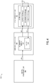
- FIG. 4 illustrates a block diagram of selected elements of an embodiment for securing an embedded controller flashing process.
- IHS 100 includes CPU 300 , EC 190 , and flash memory medium 320 .
- EC 190 includes EC memory medium 270 that further includes EC FW 274 .
- Flash memory medium 320 includes an EC region 400 that further includes a buffer region 410 , a secondary region 420 , and a primary region 430 .
- CPU 300 can send flash command 440 to EC 190 where it may be temporarily stored in EC memory medium 250 .
- EC memory medium 250 may have a limited address space such that EC memory medium 250 is unable to store an entire EC firmware update included in flash command 440 .
- flash command 440 may include an EC firmware update that is partitioned into multiple blocks of data (e.g., 1 KB data chucks) such that each block of data may include a portion of EC firmware update that has not yet been verified.
- EC 190 may then progressively send each portion of EC firmware update to flash memory medium 320 for verification. As shown in FIG.
- EC 190 may progressively send each received portion of EC firmware update from EC memory medium 250 to buffer region 410 of EC region 400 in flash memory medium 320 .
- EC 190 may perform a verification process on the entire EC firmware update. If the EC firmware update cannot be verified by EC 190 in buffer region 410 (e.g., using SHA-256), the EC firmware update may be deleted from buffer region 410 and effectively removed from flash memory medium 320 altogether such that it will not be executed by EC 190 .
- an EC firmware build server may include a private encryption key, or “private key,” used for asymmetric encryption with the public key 260 stored in EC 190 illustrated in FIG. 2 .
- the code comprising an EC firmware update may be encrypted using the private key stored in the EC firmware build server and decrypted using the public key 260 stored in EC 190 .
- the EC firmware update may be cryptographically signed using the private key stored in the EC firmware build server and verified using the public key 260 stored in EC 190 . In this way, EC 190 and the EC firmware build server can ensure that an EC firmware update is trusted and does not include malicious code that may be used for a “Denial of Service” attack, for example.
- a one-way hash function may be employed by EC 190 to verify the code comprising an EC firmware update.
- the one-way hash function may be considered collision free.
- the one-way hash function may be injective or one-to-one.
- h(z 1 ) and h(z 2 ) may produce different values, where z 1 and z 2 are different.
- a one-way hash function may be considered a cryptographic checksum, a code measurement, a digital fingerprint, a message integrity check, a contraction function, a compression function, and/or a manipulation detection code, among others.
- Examples of one-way hash functions may include one or more of an Abreast Davies-Meyer, a Davies-Meyer, a GOST Hash, a N-HASH, a HAVAL, a SHA (secure hash algorithm) (e.g., SHA-1, SHA-2, SHA-3, SHA-256, etc.), and a SNEFRU, among others.
- SHA-256 may be used to verify EC firmware updates.
- EC 190 can send the verified EC firmware update 450 to primary region 430 . That is, EC 190 may store the verified EC firmware update 450 in primary region 430 to be loaded and executed by EC 190 while a copy of the verified EC firmware update remains in buffer region 410 . The copy of the verified EC firmware update in buffer region 410 may be used as backup if the verified EC firmware update 450 becomes corrupted or otherwise invalidated for use.
- secondary region 420 may also store a copy of the verified EC firmware update that can be used as backup if the verified EC firmware update 450 stored in primary region 430 becomes corrupted or otherwise invalidated for use.
- EC 190 can simply redirect a pointer pointing to the address space of primary region 430 to point to the address space of buffer region 410 . This may allow EC 190 to access the verified EC firmware update without requiring an additional write to flash memory medium 320 (i.e., primary region 430 ).
- EC 190 can reboot and load the verified EC firmware update 450 into EC memory medium 250 to be executed.
- EC 190 can reboot which may prompt EC data 250 to locate the verified EC firmware update 450 using a pointer to primary region 430 .
- EC 190 can reverify the verified EC firmware update 450 in primary region 430 using any of the verification methods described above. If the verified EC firmware update 450 can be reverified, EC 190 can load the verified EC firmware update 450 into EC FW 274 in EC memory medium 250 such that it may be executed by EC 190 .
- EC 190 can locate and execute recovery software in secondary region 420 .
- EC data 250 can locate recovery software stored in secondary region 420 using a pointer to secondary region 420 and can verify the recovery software using any of the verification methods described above.
- EC 190 can load the recovery software into EC memory medium 200 such that it may be executed.
- recovery software may instruct EC 190 to retrieve the copy of the verified EC firmware update from buffer region 410 , reverify the copy of the verified EC firmware update in the buffer region 410 , and store the reverified copy of the verified EC firmware update in primary region 430 .
- recovery software may instruct EC 190 to request an additional EC firmware update from CPU 300 or another external non-volatile storage medium in computing environment 180 .
- flash memory medium 320 may ensure that IHS 100 can boot despite receiving an EC firmware update that has been corrupted or otherwise invalidated for use.
- FIG. 5 illustrates a flowchart of selected elements of an embodiment of a method 500 for securing an embedded controller flashing process. It is noted that certain operations described in method 500 may be optional or may be rearranged in different embodiments.
- an embedded controller (EC) 190 can receive 410 an EC firmware update from a central processing unit (CPU) 300 .
- the EC 190 can store 520 the EC firmware update into a buffer region 410 of flash memory medium 320 via bus 330 .
- Bus 330 may communicatively couple EC 190 and flash memory medium 320 while PCH 310 is in tri-state.
- EC 190 can verify 530 the EC firmware update stored in buffer region 410 of flash memory medium 320 using any of the verification methods described above.
- EC 190 can store 550 the verified EC firmware update 450 into primary region 430 of flash memory medium 320 .
- EC 190 can load 560 the verified EC firmware update 450 from primary region 430 of flash memory medium 320 into EC memory medium 200 via bus 340 such that it may be executed by EC 190 .
- FIG. 6 illustrates a flowchart of selected elements of an embodiment of a method 600 for a recovery process in response to determining that the verified EC firmware update cannot be reverified. It is noted that certain operations described in method 600 may be optional or may be rearranged in different embodiments.
- EC 190 may determine 610 that the verified EC firmware update stored in primary region 430 of flash memory medium 320 cannot be reverified. In response to determining that the verified EC firmware update cannot be reverified, EC 190 may cause 620 a recovery mode. While in recovery mode, EC 190 can load 630 recovery software stored in secondary region 420 of flash memory medium 320 , access 640 the copy of the verified EC firmware update stored in buffer region 410 of flash memory medium 320 , reverify 650 the copy of the verified EC firmware update stored in buffer region 410 , and store 660 the reverified copy of the reverified EC firmware update into primary region 430 of flash memory medium 320 .
- an apparatus or system or a component of an apparatus or system being adapted to, arranged to, capable of, configured to, enabled to, operable to, or operative to perform a particular function encompasses that apparatus, system, component, whether or not it or that particular function is activated, turned on, or unlocked, as long as that apparatus, system, or component is so adapted, arranged, capable, configured, enabled, operable, or operative.
Landscapes
- Engineering & Computer Science (AREA)
- Theoretical Computer Science (AREA)
- General Engineering & Computer Science (AREA)
- Physics & Mathematics (AREA)
- General Physics & Mathematics (AREA)
- Software Systems (AREA)
- Computer Security & Cryptography (AREA)
- Human Computer Interaction (AREA)
- Computer Hardware Design (AREA)
- Computer Networks & Wireless Communication (AREA)
- Signal Processing (AREA)
- Stored Programmes (AREA)
Abstract
Description
Claims (17)
Priority Applications (1)
| Application Number | Priority Date | Filing Date | Title |
|---|---|---|---|
| US16/527,216 US11016755B2 (en) | 2019-07-31 | 2019-07-31 | System and method to secure embedded controller flashing process |
Applications Claiming Priority (1)
| Application Number | Priority Date | Filing Date | Title |
|---|---|---|---|
| US16/527,216 US11016755B2 (en) | 2019-07-31 | 2019-07-31 | System and method to secure embedded controller flashing process |
Publications (2)
| Publication Number | Publication Date |
|---|---|
| US20210034355A1 US20210034355A1 (en) | 2021-02-04 |
| US11016755B2 true US11016755B2 (en) | 2021-05-25 |
Family
ID=74259134
Family Applications (1)
| Application Number | Title | Priority Date | Filing Date |
|---|---|---|---|
| US16/527,216 Active US11016755B2 (en) | 2019-07-31 | 2019-07-31 | System and method to secure embedded controller flashing process |
Country Status (1)
| Country | Link |
|---|---|
| US (1) | US11016755B2 (en) |
Families Citing this family (11)
| Publication number | Priority date | Publication date | Assignee | Title |
|---|---|---|---|---|
| US11231448B2 (en) | 2017-07-20 | 2022-01-25 | Targus International Llc | Systems, methods and devices for remote power management and discovery |
| EP4018644B1 (en) | 2019-08-22 | 2025-10-08 | Targus International LLC | Systems and methods for participant-controlled video conferencing |
| US20200226260A1 (en) * | 2020-03-27 | 2020-07-16 | Intel Corporation | Firmware resiliency mechanism |
| KR20220032268A (en) * | 2020-09-07 | 2022-03-15 | 에스케이하이닉스 주식회사 | Memory system and operating method of memory system |
| EP4105776B1 (en) * | 2021-06-15 | 2025-03-19 | INTEL Corporation | Method and apparatus for firmware patching |
| US12073205B2 (en) | 2021-09-14 | 2024-08-27 | Targus International Llc | Independently upgradeable docking stations |
| CN114510368A (en) * | 2022-01-17 | 2022-05-17 | 杭州加速科技有限公司 | Coding and decoding acceleration method and system based on RS erasure codes |
| FR3136079B1 (en) * | 2022-05-25 | 2025-05-30 | St Microelectronics Alps Sas | Method for managing a sensitive data area in FLASH memory |
| US12287750B2 (en) * | 2022-11-22 | 2025-04-29 | Dell Products, L.P. | Loading firmware onto an embedded controller (EC) integrated into a heterogeneous computing platform |
| KR20250090095A (en) * | 2023-12-12 | 2025-06-19 | 현대자동차주식회사 | Electronic apparatus and control method thereof |
| CN118606235A (en) * | 2024-06-26 | 2024-09-06 | 南昌华勤电子科技有限公司 | Firmware access method and system for peripheral chip of embedded controller |
Citations (72)
| Publication number | Priority date | Publication date | Assignee | Title |
|---|---|---|---|---|
| US5794054A (en) * | 1996-07-19 | 1998-08-11 | Compaq Computer Corporation | Flash ROM sharing between a processor and a controller |
| US5819087A (en) * | 1996-07-19 | 1998-10-06 | Compaq Computer Corporation | Flash ROM sharing between processor and microcontroller during booting and handling warm-booting events |
| US6357021B1 (en) * | 1999-04-14 | 2002-03-12 | Mitsumi Electric Co., Ltd. | Method and apparatus for updating firmware |
| US20020166061A1 (en) * | 2001-05-07 | 2002-11-07 | Ohad Falik | Flash memory protection scheme for secured shared BIOS implementation in personal computers with an embedded controller |
| US20040030877A1 (en) * | 2002-08-06 | 2004-02-12 | Aleksandr Frid | Using system BIOS to update embedded controller firmware |
| US20040040019A1 (en) * | 2002-08-20 | 2004-02-26 | Lg Electronics Inc. | Apparatus and method for recording firmware in computer system |
| US6708231B1 (en) * | 1999-08-12 | 2004-03-16 | Mitsumi Electric Co., Ltd. | Method and system for performing a peripheral firmware update |
| US20040076043A1 (en) * | 2002-10-21 | 2004-04-22 | Phoenix Technologies Ltd. | Reliable and secure updating and recovery of firmware from a mass storage device |
| US20050177709A1 (en) * | 2004-02-07 | 2005-08-11 | Lg Electronics Inc. | Apparatus and method for updating firmware |
| US20060075276A1 (en) * | 2004-09-30 | 2006-04-06 | Mukesh Kataria | Self-monitoring and updating of firmware over a network |
| US20060085564A1 (en) * | 2004-10-14 | 2006-04-20 | Bomhoff Matthew D | Flash mirroring |
| US20060282653A1 (en) * | 2005-06-08 | 2006-12-14 | Ping-Ying Chu | Method for updating frimware of memory card |
| US20070050465A1 (en) * | 1998-03-19 | 2007-03-01 | Canter James M | Packet capture agent for use in field assets employing shared bus architecture |
| US20070143530A1 (en) * | 2005-12-15 | 2007-06-21 | Rudelic John C | Method and apparatus for multi-block updates with secure flash memory |
| US20080086652A1 (en) * | 2006-10-10 | 2008-04-10 | Ken Krieger | Updating a power supply microcontroller |
| US20080282023A1 (en) * | 2007-05-09 | 2008-11-13 | Stmicroelectronics S.R.L. | Restoring storage devices based on flash memories and related circuit, system, and method |
| US20090187699A1 (en) * | 2008-01-23 | 2009-07-23 | Phison Electronics Corp. | Non-volatile memory storage system and method for reading an expansion read only memory image thereof |
| US20090271533A1 (en) * | 2008-04-24 | 2009-10-29 | Micron Technology, Inc. | Method and apparatus for field firmware updates in data storage systems |
| US20090307392A1 (en) * | 2008-06-10 | 2009-12-10 | Paul Mychalowych | Intelligent cable and flexible multiplexer |
| US20100023777A1 (en) * | 2007-11-12 | 2010-01-28 | Gemalto Inc | System and method for secure firmware update of a secure token having a flash memory controller and a smart card |
| US20100191867A1 (en) * | 2009-01-29 | 2010-07-29 | Dell Products L.P. | Systems and Methods for Performing Field Updates of Firmware |
| US20120072734A1 (en) * | 2010-09-22 | 2012-03-22 | Wishman Allen R | Platform firmware armoring technology |
| US20120117365A1 (en) * | 2010-11-08 | 2012-05-10 | Delta Electronics (Thailand) Public Co., Ltd. | Firmware update method and system for micro-controller unit in power supply unit |
| US20130013905A1 (en) * | 2011-07-07 | 2013-01-10 | Held James P | Bios flash attack protection and notification |
| US20130124932A1 (en) * | 2011-11-14 | 2013-05-16 | Lsi Corporation | Solid-State Disk Manufacturing Self Test |
| US20130124888A1 (en) * | 2010-06-29 | 2013-05-16 | Panasonic Corporation | Nonvolatile storage system, power supply circuit for memory system, flash memory, flash memory controller, and nonvolatile semiconductor storage device |
| US20130263262A1 (en) * | 2011-09-07 | 2013-10-03 | Jeff B. Forristal | Verifying firmware integrity of a device |
| US20140068585A1 (en) * | 2012-08-29 | 2014-03-06 | Microsoft Corporation | Secure Firmware Updates |
| US20140068594A1 (en) * | 2012-08-29 | 2014-03-06 | Microsoft Corporation | Secure firmware updates |
| US20140156872A1 (en) * | 2012-12-05 | 2014-06-05 | Broadcom Corporation | Secure element system integrated hard macro |
| US20140189669A1 (en) * | 2012-12-27 | 2014-07-03 | International Business Machines Corporation | Dynamic timeout determination for microcontroller management of firmware updates |
| US20140208047A1 (en) * | 2011-12-28 | 2014-07-24 | Balaji Vembu | Method and device to distribute code and data stores between volatile memory and non-volatile memory |
| US20140233732A1 (en) * | 2013-02-21 | 2014-08-21 | Broadcom Corporation | Mobile paytv drm architecture |
| US20140297922A1 (en) * | 2013-03-29 | 2014-10-02 | Nitin V. Sarangdhar | Method and apparatus for managing serial peripheral interface (spi) flash |
| US20150067314A1 (en) * | 2013-08-30 | 2015-03-05 | Timothy J. Strauss | Secure firmware flash controller |
| US20150280471A1 (en) * | 2014-03-28 | 2015-10-01 | Symbol Technologies, Inc. | Apparatus and method for updating remote standalone firmware |
| US20150356034A1 (en) * | 2014-06-05 | 2015-12-10 | Lenovo (Singapore) Pte. Ltd. | Embedded microcontroller and buses |
| US20150355696A1 (en) * | 2014-06-05 | 2015-12-10 | Lenovo (Singapore) Pte. Ltd. | Computer port control |
| US20160019116A1 (en) * | 2014-07-15 | 2016-01-21 | Dell Products, L.P. | Apparatus and method for recovering an information handling system from a non-operational state |
| US20160055068A1 (en) * | 2013-04-23 | 2016-02-25 | Hewlett-Packard Development Company, L.P. | Recovering from Compromised System Boot Code |
| US20160055332A1 (en) * | 2013-04-23 | 2016-02-25 | Hewlett- Packard Development Company, L.P. | Verifying Controller Code and System Boot Code |
| US20160063254A1 (en) * | 2013-04-23 | 2016-03-03 | Hewlett-Packard Development Company, L.P. | Retrieving System Boot Code from a Non-Volatile Memory |
| US20160063255A1 (en) * | 2013-04-23 | 2016-03-03 | Hewlett-Packard Development Company, L.P. | Event Data Structure to Store Event Data |
| US20160306977A1 (en) * | 2014-12-22 | 2016-10-20 | Capital One Services, LLC. | System and methods for secure firmware validation |
| US20160350538A1 (en) * | 2015-05-25 | 2016-12-01 | Insyde Software Corp. | Embedded controller for safety booting and method thereof |
| US20170094377A1 (en) * | 2015-09-25 | 2017-03-30 | Andrew J. Herdrich | Out-of-band platform tuning and configuration |
| US20170123721A1 (en) * | 2015-10-28 | 2017-05-04 | Sandisk Technologies Inc. | System and method for utilization of a data buffer by command completion in parts |
| US20170126143A1 (en) * | 2015-10-30 | 2017-05-04 | Vapor IO Inc. | Bus bar power adapter for ac-input, hot-swap power supplies |
| US20170123722A1 (en) * | 2015-10-28 | 2017-05-04 | Sandisk Technologies Inc. | System and method for utilization of a data buffer |
| US20170123991A1 (en) * | 2015-10-28 | 2017-05-04 | Sandisk Technologies Inc. | System and method for utilization of a data buffer in a storage device |
| US20170206077A1 (en) * | 2014-07-02 | 2017-07-20 | Hewlett-Packard Development Company, L.P. | Firmware update |
| US20170249155A1 (en) * | 2016-02-26 | 2017-08-31 | Sandisk Technologies Inc. | Memory System and Method for Fast Firmware Download |
| US20170255459A1 (en) * | 2016-03-01 | 2017-09-07 | Renesas Electronics Corporation | Embedded device and program updating method |
| US20170293484A1 (en) * | 2016-04-11 | 2017-10-12 | Endress+Hauser Conducta Gmbh+Co. Kg | Method for updating a firmware component and device of measurement and control technology |
| US20170300107A1 (en) * | 2016-04-15 | 2017-10-19 | Emerson Climate Technologies, Inc. | Microcontroller Architecture for Power Factor Correction Converter |
| US20180165455A1 (en) * | 2016-12-13 | 2018-06-14 | Amazon Technologies, Inc. | Secure execution environment on a server |
| US20180225459A1 (en) * | 2015-04-14 | 2018-08-09 | Capital One Services, Llc | System and methods for secure firmware validation |
| US20180232521A1 (en) * | 2016-01-25 | 2018-08-16 | Hewlett-Packard Development Company, L.P. | Notice of intrusion into firmware |
| US20180351749A1 (en) * | 2017-06-01 | 2018-12-06 | Silicon Motion, Inc. | Data Storage Devices and Methods for Encrypting and Decrypting a Firmware File Thereof |
| US20190042228A1 (en) * | 2017-12-28 | 2019-02-07 | Intel Corporation | Firmware upgrade method and apparatus |
| US20190042229A1 (en) * | 2018-08-16 | 2019-02-07 | Intel Corporation | Soc-assisted resilient boot |
| US20190129638A1 (en) * | 2017-10-26 | 2019-05-02 | Redpine Signals, Inc. | Memory interface for a Secure NOR Flash Memory |
| US20190179568A1 (en) * | 2017-12-08 | 2019-06-13 | Sandisk Technologies Llc | Microcontroller instruction memory architecture for non-volatile memory |
| US20190179532A1 (en) * | 2017-12-08 | 2019-06-13 | Sandisk Technologies Llc | Signal reduction in a microcontroller architecture for non-volatile memory |
| US20190179573A1 (en) * | 2017-12-08 | 2019-06-13 | Sandisk Technologies Llc | Microcontroller architecture for non-volatile memory |
| US20190227783A1 (en) * | 2018-01-23 | 2019-07-25 | Wistron Corporation | Electronic apparatus and firmware update method thereof |
| US20190286483A1 (en) * | 2018-03-14 | 2019-09-19 | Texas Instruments Incorporated | Thread scheduling for multithreaded data processing environments |
| US20190386966A1 (en) * | 2018-06-19 | 2019-12-19 | Cypress Semiconductor Corporation | Secured communication from within non-volatile memory device |
| US20200082089A1 (en) * | 2018-09-06 | 2020-03-12 | Micron Technology, Inc. | Secure boot via system and power management microcontroller |
| US10678529B1 (en) * | 2017-11-30 | 2020-06-09 | Amazon Technologies, Inc. | Secure device firmware installation |
| US20200201692A1 (en) * | 2018-12-21 | 2020-06-25 | Samsung Electronics Co., Ltd. | System and method for offloading application functions to a device |
| US20200293298A1 (en) * | 2019-03-13 | 2020-09-17 | Microsoft Technology Licensing, Llc | Firmware update system |
-
2019
- 2019-07-31 US US16/527,216 patent/US11016755B2/en active Active
Patent Citations (76)
| Publication number | Priority date | Publication date | Assignee | Title |
|---|---|---|---|---|
| US5794054A (en) * | 1996-07-19 | 1998-08-11 | Compaq Computer Corporation | Flash ROM sharing between a processor and a controller |
| US5819087A (en) * | 1996-07-19 | 1998-10-06 | Compaq Computer Corporation | Flash ROM sharing between processor and microcontroller during booting and handling warm-booting events |
| US20070050465A1 (en) * | 1998-03-19 | 2007-03-01 | Canter James M | Packet capture agent for use in field assets employing shared bus architecture |
| US6357021B1 (en) * | 1999-04-14 | 2002-03-12 | Mitsumi Electric Co., Ltd. | Method and apparatus for updating firmware |
| US6708231B1 (en) * | 1999-08-12 | 2004-03-16 | Mitsumi Electric Co., Ltd. | Method and system for performing a peripheral firmware update |
| US20020166061A1 (en) * | 2001-05-07 | 2002-11-07 | Ohad Falik | Flash memory protection scheme for secured shared BIOS implementation in personal computers with an embedded controller |
| US20040030877A1 (en) * | 2002-08-06 | 2004-02-12 | Aleksandr Frid | Using system BIOS to update embedded controller firmware |
| US7171658B2 (en) * | 2002-08-20 | 2007-01-30 | Lg Electronics Inc. | Apparatus and method for recording firmware in computer system |
| US20040040019A1 (en) * | 2002-08-20 | 2004-02-26 | Lg Electronics Inc. | Apparatus and method for recording firmware in computer system |
| US20040076043A1 (en) * | 2002-10-21 | 2004-04-22 | Phoenix Technologies Ltd. | Reliable and secure updating and recovery of firmware from a mass storage device |
| US20050177709A1 (en) * | 2004-02-07 | 2005-08-11 | Lg Electronics Inc. | Apparatus and method for updating firmware |
| US20060075276A1 (en) * | 2004-09-30 | 2006-04-06 | Mukesh Kataria | Self-monitoring and updating of firmware over a network |
| US20060085564A1 (en) * | 2004-10-14 | 2006-04-20 | Bomhoff Matthew D | Flash mirroring |
| US20060282653A1 (en) * | 2005-06-08 | 2006-12-14 | Ping-Ying Chu | Method for updating frimware of memory card |
| US20070143530A1 (en) * | 2005-12-15 | 2007-06-21 | Rudelic John C | Method and apparatus for multi-block updates with secure flash memory |
| US20080086652A1 (en) * | 2006-10-10 | 2008-04-10 | Ken Krieger | Updating a power supply microcontroller |
| US20080282023A1 (en) * | 2007-05-09 | 2008-11-13 | Stmicroelectronics S.R.L. | Restoring storage devices based on flash memories and related circuit, system, and method |
| US20100023777A1 (en) * | 2007-11-12 | 2010-01-28 | Gemalto Inc | System and method for secure firmware update of a secure token having a flash memory controller and a smart card |
| US20090187699A1 (en) * | 2008-01-23 | 2009-07-23 | Phison Electronics Corp. | Non-volatile memory storage system and method for reading an expansion read only memory image thereof |
| US20090271533A1 (en) * | 2008-04-24 | 2009-10-29 | Micron Technology, Inc. | Method and apparatus for field firmware updates in data storage systems |
| US20090307392A1 (en) * | 2008-06-10 | 2009-12-10 | Paul Mychalowych | Intelligent cable and flexible multiplexer |
| US20100191867A1 (en) * | 2009-01-29 | 2010-07-29 | Dell Products L.P. | Systems and Methods for Performing Field Updates of Firmware |
| US20130124888A1 (en) * | 2010-06-29 | 2013-05-16 | Panasonic Corporation | Nonvolatile storage system, power supply circuit for memory system, flash memory, flash memory controller, and nonvolatile semiconductor storage device |
| US20120072734A1 (en) * | 2010-09-22 | 2012-03-22 | Wishman Allen R | Platform firmware armoring technology |
| US20120117365A1 (en) * | 2010-11-08 | 2012-05-10 | Delta Electronics (Thailand) Public Co., Ltd. | Firmware update method and system for micro-controller unit in power supply unit |
| US20130013905A1 (en) * | 2011-07-07 | 2013-01-10 | Held James P | Bios flash attack protection and notification |
| US20130263262A1 (en) * | 2011-09-07 | 2013-10-03 | Jeff B. Forristal | Verifying firmware integrity of a device |
| US20130124932A1 (en) * | 2011-11-14 | 2013-05-16 | Lsi Corporation | Solid-State Disk Manufacturing Self Test |
| US20140208047A1 (en) * | 2011-12-28 | 2014-07-24 | Balaji Vembu | Method and device to distribute code and data stores between volatile memory and non-volatile memory |
| US20140068585A1 (en) * | 2012-08-29 | 2014-03-06 | Microsoft Corporation | Secure Firmware Updates |
| US20140068594A1 (en) * | 2012-08-29 | 2014-03-06 | Microsoft Corporation | Secure firmware updates |
| US20140156872A1 (en) * | 2012-12-05 | 2014-06-05 | Broadcom Corporation | Secure element system integrated hard macro |
| US20140189669A1 (en) * | 2012-12-27 | 2014-07-03 | International Business Machines Corporation | Dynamic timeout determination for microcontroller management of firmware updates |
| US9477458B2 (en) * | 2012-12-27 | 2016-10-25 | Lenovo Enterprise Solutions (Singapore) Pte. Ltd. | Dynamic timeout determination for microcontroller management of firmware updates |
| US20140233732A1 (en) * | 2013-02-21 | 2014-08-21 | Broadcom Corporation | Mobile paytv drm architecture |
| US20140297922A1 (en) * | 2013-03-29 | 2014-10-02 | Nitin V. Sarangdhar | Method and apparatus for managing serial peripheral interface (spi) flash |
| US10733288B2 (en) * | 2013-04-23 | 2020-08-04 | Hewlett-Packard Development Company, L.P. | Verifying controller code and system boot code |
| US20160063255A1 (en) * | 2013-04-23 | 2016-03-03 | Hewlett-Packard Development Company, L.P. | Event Data Structure to Store Event Data |
| US20160055068A1 (en) * | 2013-04-23 | 2016-02-25 | Hewlett-Packard Development Company, L.P. | Recovering from Compromised System Boot Code |
| US20160055332A1 (en) * | 2013-04-23 | 2016-02-25 | Hewlett- Packard Development Company, L.P. | Verifying Controller Code and System Boot Code |
| US20160063254A1 (en) * | 2013-04-23 | 2016-03-03 | Hewlett-Packard Development Company, L.P. | Retrieving System Boot Code from a Non-Volatile Memory |
| US20150067314A1 (en) * | 2013-08-30 | 2015-03-05 | Timothy J. Strauss | Secure firmware flash controller |
| US20150280471A1 (en) * | 2014-03-28 | 2015-10-01 | Symbol Technologies, Inc. | Apparatus and method for updating remote standalone firmware |
| US20150355696A1 (en) * | 2014-06-05 | 2015-12-10 | Lenovo (Singapore) Pte. Ltd. | Computer port control |
| US20150356034A1 (en) * | 2014-06-05 | 2015-12-10 | Lenovo (Singapore) Pte. Ltd. | Embedded microcontroller and buses |
| US20170206077A1 (en) * | 2014-07-02 | 2017-07-20 | Hewlett-Packard Development Company, L.P. | Firmware update |
| US9891996B2 (en) * | 2014-07-15 | 2018-02-13 | Dell Poducts, L.P. | Apparatus and method for recovering an information handling system from a non-operational state |
| US20160019116A1 (en) * | 2014-07-15 | 2016-01-21 | Dell Products, L.P. | Apparatus and method for recovering an information handling system from a non-operational state |
| US20160306977A1 (en) * | 2014-12-22 | 2016-10-20 | Capital One Services, LLC. | System and methods for secure firmware validation |
| US20180225459A1 (en) * | 2015-04-14 | 2018-08-09 | Capital One Services, Llc | System and methods for secure firmware validation |
| US20160350538A1 (en) * | 2015-05-25 | 2016-12-01 | Insyde Software Corp. | Embedded controller for safety booting and method thereof |
| US20170094377A1 (en) * | 2015-09-25 | 2017-03-30 | Andrew J. Herdrich | Out-of-band platform tuning and configuration |
| US20170123721A1 (en) * | 2015-10-28 | 2017-05-04 | Sandisk Technologies Inc. | System and method for utilization of a data buffer by command completion in parts |
| US20170123722A1 (en) * | 2015-10-28 | 2017-05-04 | Sandisk Technologies Inc. | System and method for utilization of a data buffer |
| US20170123991A1 (en) * | 2015-10-28 | 2017-05-04 | Sandisk Technologies Inc. | System and method for utilization of a data buffer in a storage device |
| US20170126143A1 (en) * | 2015-10-30 | 2017-05-04 | Vapor IO Inc. | Bus bar power adapter for ac-input, hot-swap power supplies |
| US20180232521A1 (en) * | 2016-01-25 | 2018-08-16 | Hewlett-Packard Development Company, L.P. | Notice of intrusion into firmware |
| US20170249155A1 (en) * | 2016-02-26 | 2017-08-31 | Sandisk Technologies Inc. | Memory System and Method for Fast Firmware Download |
| US20170255459A1 (en) * | 2016-03-01 | 2017-09-07 | Renesas Electronics Corporation | Embedded device and program updating method |
| US20170293484A1 (en) * | 2016-04-11 | 2017-10-12 | Endress+Hauser Conducta Gmbh+Co. Kg | Method for updating a firmware component and device of measurement and control technology |
| US20170300107A1 (en) * | 2016-04-15 | 2017-10-19 | Emerson Climate Technologies, Inc. | Microcontroller Architecture for Power Factor Correction Converter |
| US20180165455A1 (en) * | 2016-12-13 | 2018-06-14 | Amazon Technologies, Inc. | Secure execution environment on a server |
| US20180351749A1 (en) * | 2017-06-01 | 2018-12-06 | Silicon Motion, Inc. | Data Storage Devices and Methods for Encrypting and Decrypting a Firmware File Thereof |
| US20190129638A1 (en) * | 2017-10-26 | 2019-05-02 | Redpine Signals, Inc. | Memory interface for a Secure NOR Flash Memory |
| US10678529B1 (en) * | 2017-11-30 | 2020-06-09 | Amazon Technologies, Inc. | Secure device firmware installation |
| US20190179568A1 (en) * | 2017-12-08 | 2019-06-13 | Sandisk Technologies Llc | Microcontroller instruction memory architecture for non-volatile memory |
| US20190179532A1 (en) * | 2017-12-08 | 2019-06-13 | Sandisk Technologies Llc | Signal reduction in a microcontroller architecture for non-volatile memory |
| US20190179573A1 (en) * | 2017-12-08 | 2019-06-13 | Sandisk Technologies Llc | Microcontroller architecture for non-volatile memory |
| US20190042228A1 (en) * | 2017-12-28 | 2019-02-07 | Intel Corporation | Firmware upgrade method and apparatus |
| US20190227783A1 (en) * | 2018-01-23 | 2019-07-25 | Wistron Corporation | Electronic apparatus and firmware update method thereof |
| US20190286483A1 (en) * | 2018-03-14 | 2019-09-19 | Texas Instruments Incorporated | Thread scheduling for multithreaded data processing environments |
| US20190386966A1 (en) * | 2018-06-19 | 2019-12-19 | Cypress Semiconductor Corporation | Secured communication from within non-volatile memory device |
| US20190042229A1 (en) * | 2018-08-16 | 2019-02-07 | Intel Corporation | Soc-assisted resilient boot |
| US20200082089A1 (en) * | 2018-09-06 | 2020-03-12 | Micron Technology, Inc. | Secure boot via system and power management microcontroller |
| US20200201692A1 (en) * | 2018-12-21 | 2020-06-25 | Samsung Electronics Co., Ltd. | System and method for offloading application functions to a device |
| US20200293298A1 (en) * | 2019-03-13 | 2020-09-17 | Microsoft Technology Licensing, Llc | Firmware update system |
Non-Patent Citations (2)
| Title |
|---|
| Dennis K. Nilsson et al., A Framework for Self-Verification of Firmware Updates over the Air in Vehicle ECUs, 2008 IEEE, [Retrieved on Feb. 12, 2021], Retrieved from the internet: <URL: https://ieeexplore.ieee.org/stamp/stamp.jsp?tp=&arnumber=4746641> 5 Pages (1-5) (Year: 2008). * |
| Lucille R. McMinn, External Verification of SCADA System Embedded Controller Firmware, Mar. 22, 2012, [Retrieved on Feb. 12, 2021], Retrieved from the internet: <URL: https://scholar.afit.edu/cgi/viewcontent.cgi?article=2138&context=etd> 100 Pages (1-100) (Year: 2012). * |
Also Published As
| Publication number | Publication date |
|---|---|
| US20210034355A1 (en) | 2021-02-04 |
Similar Documents
| Publication | Publication Date | Title |
|---|---|---|
| US11016755B2 (en) | System and method to secure embedded controller flashing process | |
| JP5970141B2 (en) | Method, boot loader, user trusted device, and system for executing software modules on a computer | |
| US12531734B2 (en) | Certifying authenticity of stored code and code updates | |
| US10387336B2 (en) | Memory protection based on system state | |
| US20160078212A1 (en) | Hypervisor and virtual machine protection | |
| CN105593866B (en) | Terminal authentication and register system, terminal authentication and register method and storage medium | |
| US20210334378A1 (en) | System and method of authenticating firmware | |
| CN111510424B (en) | Secure multi-party computing framework using restricted operating environment with guest agent | |
| US10853498B2 (en) | Secure boot orchestration device in a virtual desktop infrastructure | |
| US11431506B2 (en) | System and method of utilizing a component of an information handling system | |
| US9489212B2 (en) | System and method for an access controller assisted boot | |
| US11757859B2 (en) | Run-time attestation of a user workspace | |
| US20250036813A1 (en) | Managing threats to data storage in distributed environments | |
| US11307869B2 (en) | Identifying a transport route using an information handling system firmware driver | |
| CN114861207B (en) | Data processing method, device, electronic device and computer readable storage medium | |
| US20200143059A1 (en) | Chassis internal device security | |
| US10805302B2 (en) | Systems and methods to secure platform application services between platform client applications and platform services | |
| US20250056023A1 (en) | Codec management at an information handling system | |
| US20220237023A1 (en) | System and method of utilizing platform applications with information handling systems | |
| US11153320B2 (en) | Invariant detection using distributed ledgers | |
| CN111510423B (en) | Token-based secure multi-party computing framework using restricted operating environments | |
| US10740035B1 (en) | System and method for controlling management commands at devices | |
| US12206676B2 (en) | Providing access control to distributed resources to an information handling system | |
| US12407515B2 (en) | Codec management at an information handling system | |
| US20250356062A1 (en) | Managing trusted platform module (tpm) replacement at an information handling system |
Legal Events
| Date | Code | Title | Description |
|---|---|---|---|
| AS | Assignment |
Owner name: DELL PRODUCTS L.P., TEXAS Free format text: ASSIGNMENT OF ASSIGNORS INTEREST;ASSIGNOR:MONTERO, ADOLFO S.;REEL/FRAME:049912/0634 Effective date: 20190729 |
|
| FEPP | Fee payment procedure |
Free format text: ENTITY STATUS SET TO UNDISCOUNTED (ORIGINAL EVENT CODE: BIG.); ENTITY STATUS OF PATENT OWNER: LARGE ENTITY |
|
| AS | Assignment |
Owner name: CREDIT SUISSE AG, CAYMAN ISLANDS BRANCH, NORTH CAROLINA Free format text: SECURITY AGREEMENT;ASSIGNORS:DELL PRODUCTS L.P.;EMC CORPORATION;EMC IP HOLDING COMPANY LLC;REEL/FRAME:050406/0421 Effective date: 20190917 |
|
| AS | Assignment |
Owner name: THE BANK OF NEW YORK MELLON TRUST COMPANY, N.A., AS COLLATERAL AGENT, TEXAS Free format text: PATENT SECURITY AGREEMENT (NOTES);ASSIGNORS:DELL PRODUCTS L.P.;EMC CORPORATION;EMC IP HOLDING COMPANY LLC;REEL/FRAME:050724/0571 Effective date: 20191010 |
|
| AS | Assignment |
Owner name: THE BANK OF NEW YORK MELLON TRUST COMPANY, N.A., TEXAS Free format text: SECURITY AGREEMENT;ASSIGNORS:CREDANT TECHNOLOGIES INC.;DELL INTERNATIONAL L.L.C.;DELL MARKETING L.P.;AND OTHERS;REEL/FRAME:053546/0001 Effective date: 20200409 |
|
| AS | Assignment |
Owner name: THE BANK OF NEW YORK MELLON TRUST COMPANY, N.A., AS COLLATERAL AGENT, TEXAS Free format text: SECURITY INTEREST;ASSIGNORS:DELL PRODUCTS L.P.;EMC CORPORATION;EMC IP HOLDING COMPANY LLC;REEL/FRAME:053311/0169 Effective date: 20200603 |
|
| STPP | Information on status: patent application and granting procedure in general |
Free format text: DOCKETED NEW CASE - READY FOR EXAMINATION |
|
| STPP | Information on status: patent application and granting procedure in general |
Free format text: NOTICE OF ALLOWANCE MAILED -- APPLICATION RECEIVED IN OFFICE OF PUBLICATIONS |
|
| STPP | Information on status: patent application and granting procedure in general |
Free format text: PUBLICATIONS -- ISSUE FEE PAYMENT RECEIVED |
|
| STPP | Information on status: patent application and granting procedure in general |
Free format text: PUBLICATIONS -- ISSUE FEE PAYMENT VERIFIED |
|
| STCF | Information on status: patent grant |
Free format text: PATENTED CASE |
|
| AS | Assignment |
Owner name: EMC IP HOLDING COMPANY LLC, TEXAS Free format text: RELEASE OF SECURITY INTEREST AT REEL 050406 FRAME 421;ASSIGNOR:CREDIT SUISSE AG, CAYMAN ISLANDS BRANCH;REEL/FRAME:058213/0825 Effective date: 20211101 Owner name: EMC CORPORATION, MASSACHUSETTS Free format text: RELEASE OF SECURITY INTEREST AT REEL 050406 FRAME 421;ASSIGNOR:CREDIT SUISSE AG, CAYMAN ISLANDS BRANCH;REEL/FRAME:058213/0825 Effective date: 20211101 Owner name: DELL PRODUCTS L.P., TEXAS Free format text: RELEASE OF SECURITY INTEREST AT REEL 050406 FRAME 421;ASSIGNOR:CREDIT SUISSE AG, CAYMAN ISLANDS BRANCH;REEL/FRAME:058213/0825 Effective date: 20211101 |
|
| AS | Assignment |
Owner name: EMC IP HOLDING COMPANY LLC, TEXAS Free format text: RELEASE OF SECURITY INTEREST IN PATENTS PREVIOUSLY RECORDED AT REEL/FRAME (053311/0169);ASSIGNOR:THE BANK OF NEW YORK MELLON TRUST COMPANY, N.A., AS NOTES COLLATERAL AGENT;REEL/FRAME:060438/0742 Effective date: 20220329 Owner name: EMC CORPORATION, MASSACHUSETTS Free format text: RELEASE OF SECURITY INTEREST IN PATENTS PREVIOUSLY RECORDED AT REEL/FRAME (053311/0169);ASSIGNOR:THE BANK OF NEW YORK MELLON TRUST COMPANY, N.A., AS NOTES COLLATERAL AGENT;REEL/FRAME:060438/0742 Effective date: 20220329 Owner name: DELL PRODUCTS L.P., TEXAS Free format text: RELEASE OF SECURITY INTEREST IN PATENTS PREVIOUSLY RECORDED AT REEL/FRAME (053311/0169);ASSIGNOR:THE BANK OF NEW YORK MELLON TRUST COMPANY, N.A., AS NOTES COLLATERAL AGENT;REEL/FRAME:060438/0742 Effective date: 20220329 Owner name: EMC IP HOLDING COMPANY LLC, TEXAS Free format text: RELEASE OF SECURITY INTEREST IN PATENTS PREVIOUSLY RECORDED AT REEL/FRAME (050724/0571);ASSIGNOR:THE BANK OF NEW YORK MELLON TRUST COMPANY, N.A., AS NOTES COLLATERAL AGENT;REEL/FRAME:060436/0088 Effective date: 20220329 Owner name: EMC CORPORATION, MASSACHUSETTS Free format text: RELEASE OF SECURITY INTEREST IN PATENTS PREVIOUSLY RECORDED AT REEL/FRAME (050724/0571);ASSIGNOR:THE BANK OF NEW YORK MELLON TRUST COMPANY, N.A., AS NOTES COLLATERAL AGENT;REEL/FRAME:060436/0088 Effective date: 20220329 Owner name: DELL PRODUCTS L.P., TEXAS Free format text: RELEASE OF SECURITY INTEREST IN PATENTS PREVIOUSLY RECORDED AT REEL/FRAME (050724/0571);ASSIGNOR:THE BANK OF NEW YORK MELLON TRUST COMPANY, N.A., AS NOTES COLLATERAL AGENT;REEL/FRAME:060436/0088 Effective date: 20220329 Owner name: DELL MARKETING L.P. (ON BEHALF OF ITSELF AND AS SUCCESSOR-IN-INTEREST TO CREDANT TECHNOLOGIES, INC.), TEXAS Free format text: RELEASE OF SECURITY INTEREST IN PATENTS PREVIOUSLY RECORDED AT REEL/FRAME (053546/0001);ASSIGNOR:THE BANK OF NEW YORK MELLON TRUST COMPANY, N.A., AS NOTES COLLATERAL AGENT;REEL/FRAME:071642/0001 Effective date: 20220329 Owner name: DELL INTERNATIONAL L.L.C., TEXAS Free format text: RELEASE OF SECURITY INTEREST IN PATENTS PREVIOUSLY RECORDED AT REEL/FRAME (053546/0001);ASSIGNOR:THE BANK OF NEW YORK MELLON TRUST COMPANY, N.A., AS NOTES COLLATERAL AGENT;REEL/FRAME:071642/0001 Effective date: 20220329 Owner name: DELL PRODUCTS L.P., TEXAS Free format text: RELEASE OF SECURITY INTEREST IN PATENTS PREVIOUSLY RECORDED AT REEL/FRAME (053546/0001);ASSIGNOR:THE BANK OF NEW YORK MELLON TRUST COMPANY, N.A., AS NOTES COLLATERAL AGENT;REEL/FRAME:071642/0001 Effective date: 20220329 Owner name: DELL USA L.P., TEXAS Free format text: RELEASE OF SECURITY INTEREST IN PATENTS PREVIOUSLY RECORDED AT REEL/FRAME (053546/0001);ASSIGNOR:THE BANK OF NEW YORK MELLON TRUST COMPANY, N.A., AS NOTES COLLATERAL AGENT;REEL/FRAME:071642/0001 Effective date: 20220329 Owner name: EMC CORPORATION, MASSACHUSETTS Free format text: RELEASE OF SECURITY INTEREST IN PATENTS PREVIOUSLY RECORDED AT REEL/FRAME (053546/0001);ASSIGNOR:THE BANK OF NEW YORK MELLON TRUST COMPANY, N.A., AS NOTES COLLATERAL AGENT;REEL/FRAME:071642/0001 Effective date: 20220329 Owner name: DELL MARKETING CORPORATION (SUCCESSOR-IN-INTEREST TO FORCE10 NETWORKS, INC. AND WYSE TECHNOLOGY L.L.C.), TEXAS Free format text: RELEASE OF SECURITY INTEREST IN PATENTS PREVIOUSLY RECORDED AT REEL/FRAME (053546/0001);ASSIGNOR:THE BANK OF NEW YORK MELLON TRUST COMPANY, N.A., AS NOTES COLLATERAL AGENT;REEL/FRAME:071642/0001 Effective date: 20220329 Owner name: EMC IP HOLDING COMPANY LLC, TEXAS Free format text: RELEASE OF SECURITY INTEREST IN PATENTS PREVIOUSLY RECORDED AT REEL/FRAME (053546/0001);ASSIGNOR:THE BANK OF NEW YORK MELLON TRUST COMPANY, N.A., AS NOTES COLLATERAL AGENT;REEL/FRAME:071642/0001 Effective date: 20220329 |
|
| MAFP | Maintenance fee payment |
Free format text: PAYMENT OF MAINTENANCE FEE, 4TH YEAR, LARGE ENTITY (ORIGINAL EVENT CODE: M1551); ENTITY STATUS OF PATENT OWNER: LARGE ENTITY Year of fee payment: 4 |