US11015241B2 - Reaction of diazadiene complexes with amines - Google Patents
Reaction of diazadiene complexes with amines Download PDFInfo
- Publication number
- US11015241B2 US11015241B2 US16/307,608 US201716307608A US11015241B2 US 11015241 B2 US11015241 B2 US 11015241B2 US 201716307608 A US201716307608 A US 201716307608A US 11015241 B2 US11015241 B2 US 11015241B2
- Authority
- US
- United States
- Prior art keywords
- amine
- metal
- butyl
- alkyl
- tert
- Prior art date
- Legal status (The legal status is an assumption and is not a legal conclusion. Google has not performed a legal analysis and makes no representation as to the accuracy of the status listed.)
- Active, expires
Links
- 0 [1*]NC([2*])C([3*])N[1*] Chemical compound [1*]NC([2*])C([3*])N[1*] 0.000 description 14
Images


Classifications
-
- C—CHEMISTRY; METALLURGY
- C23—COATING METALLIC MATERIAL; COATING MATERIAL WITH METALLIC MATERIAL; CHEMICAL SURFACE TREATMENT; DIFFUSION TREATMENT OF METALLIC MATERIAL; COATING BY VACUUM EVAPORATION, BY SPUTTERING, BY ION IMPLANTATION OR BY CHEMICAL VAPOUR DEPOSITION, IN GENERAL; INHIBITING CORROSION OF METALLIC MATERIAL OR INCRUSTATION IN GENERAL
- C23C—COATING METALLIC MATERIAL; COATING MATERIAL WITH METALLIC MATERIAL; SURFACE TREATMENT OF METALLIC MATERIAL BY DIFFUSION INTO THE SURFACE, BY CHEMICAL CONVERSION OR SUBSTITUTION; COATING BY VACUUM EVAPORATION, BY SPUTTERING, BY ION IMPLANTATION OR BY CHEMICAL VAPOUR DEPOSITION, IN GENERAL
- C23C16/00—Chemical coating by decomposition of gaseous compounds, without leaving reaction products of surface material in the coating, i.e. chemical vapour deposition [CVD] processes
- C23C16/06—Chemical coating by decomposition of gaseous compounds, without leaving reaction products of surface material in the coating, i.e. chemical vapour deposition [CVD] processes characterised by the deposition of metallic material
- C23C16/18—Chemical coating by decomposition of gaseous compounds, without leaving reaction products of surface material in the coating, i.e. chemical vapour deposition [CVD] processes characterised by the deposition of metallic material from metallo-organic compounds
-
- C—CHEMISTRY; METALLURGY
- C23—COATING METALLIC MATERIAL; COATING MATERIAL WITH METALLIC MATERIAL; CHEMICAL SURFACE TREATMENT; DIFFUSION TREATMENT OF METALLIC MATERIAL; COATING BY VACUUM EVAPORATION, BY SPUTTERING, BY ION IMPLANTATION OR BY CHEMICAL VAPOUR DEPOSITION, IN GENERAL; INHIBITING CORROSION OF METALLIC MATERIAL OR INCRUSTATION IN GENERAL
- C23C—COATING METALLIC MATERIAL; COATING MATERIAL WITH METALLIC MATERIAL; SURFACE TREATMENT OF METALLIC MATERIAL BY DIFFUSION INTO THE SURFACE, BY CHEMICAL CONVERSION OR SUBSTITUTION; COATING BY VACUUM EVAPORATION, BY SPUTTERING, BY ION IMPLANTATION OR BY CHEMICAL VAPOUR DEPOSITION, IN GENERAL
- C23C16/00—Chemical coating by decomposition of gaseous compounds, without leaving reaction products of surface material in the coating, i.e. chemical vapour deposition [CVD] processes
- C23C16/44—Chemical coating by decomposition of gaseous compounds, without leaving reaction products of surface material in the coating, i.e. chemical vapour deposition [CVD] processes characterised by the method of coating
- C23C16/448—Chemical coating by decomposition of gaseous compounds, without leaving reaction products of surface material in the coating, i.e. chemical vapour deposition [CVD] processes characterised by the method of coating characterised by the method used for generating reactive gas streams, e.g. by evaporation or sublimation of precursor materials
- C23C16/4488—Chemical coating by decomposition of gaseous compounds, without leaving reaction products of surface material in the coating, i.e. chemical vapour deposition [CVD] processes characterised by the method of coating characterised by the method used for generating reactive gas streams, e.g. by evaporation or sublimation of precursor materials by in situ generation of reactive gas by chemical or electrochemical reaction
-
- C—CHEMISTRY; METALLURGY
- C23—COATING METALLIC MATERIAL; COATING MATERIAL WITH METALLIC MATERIAL; CHEMICAL SURFACE TREATMENT; DIFFUSION TREATMENT OF METALLIC MATERIAL; COATING BY VACUUM EVAPORATION, BY SPUTTERING, BY ION IMPLANTATION OR BY CHEMICAL VAPOUR DEPOSITION, IN GENERAL; INHIBITING CORROSION OF METALLIC MATERIAL OR INCRUSTATION IN GENERAL
- C23C—COATING METALLIC MATERIAL; COATING MATERIAL WITH METALLIC MATERIAL; SURFACE TREATMENT OF METALLIC MATERIAL BY DIFFUSION INTO THE SURFACE, BY CHEMICAL CONVERSION OR SUBSTITUTION; COATING BY VACUUM EVAPORATION, BY SPUTTERING, BY ION IMPLANTATION OR BY CHEMICAL VAPOUR DEPOSITION, IN GENERAL
- C23C16/00—Chemical coating by decomposition of gaseous compounds, without leaving reaction products of surface material in the coating, i.e. chemical vapour deposition [CVD] processes
- C23C16/44—Chemical coating by decomposition of gaseous compounds, without leaving reaction products of surface material in the coating, i.e. chemical vapour deposition [CVD] processes characterised by the method of coating
- C23C16/455—Chemical coating by decomposition of gaseous compounds, without leaving reaction products of surface material in the coating, i.e. chemical vapour deposition [CVD] processes characterised by the method of coating characterised by the method used for introducing gases into reaction chamber or for modifying gas flows in reaction chamber
- C23C16/45523—Pulsed gas flow or change of composition over time
- C23C16/45525—Atomic layer deposition [ALD]
- C23C16/45553—Atomic layer deposition [ALD] characterized by the use of precursors specially adapted for ALD
-
- C—CHEMISTRY; METALLURGY
- C07—ORGANIC CHEMISTRY
- C07F—ACYCLIC, CARBOCYCLIC OR HETEROCYCLIC COMPOUNDS CONTAINING ELEMENTS OTHER THAN CARBON, HYDROGEN, HALOGEN, OXYGEN, NITROGEN, SULFUR, SELENIUM OR TELLURIUM
- C07F15/00—Compounds containing elements of Groups 8, 9, 10 or 18 of the Periodic Table
- C07F15/04—Nickel compounds
- C07F15/045—Nickel compounds without a metal-carbon linkage
-
- C—CHEMISTRY; METALLURGY
- C07—ORGANIC CHEMISTRY
- C07F—ACYCLIC, CARBOCYCLIC OR HETEROCYCLIC COMPOUNDS CONTAINING ELEMENTS OTHER THAN CARBON, HYDROGEN, HALOGEN, OXYGEN, NITROGEN, SULFUR, SELENIUM OR TELLURIUM
- C07F15/00—Compounds containing elements of Groups 8, 9, 10 or 18 of the Periodic Table
- C07F15/06—Cobalt compounds
- C07F15/065—Cobalt compounds without a metal-carbon linkage
Definitions
- the present invention relates to methods of depositing metal layers on a substrate.
- the semiconductor industry has mandated a continuous reduction in microelectronics feature sizes from 65 nm in 2006 to ⁇ 10 nm in 2017.
- This push toward smaller feature sizes requires controlled growth of films as thin as 1 nm.
- two-dimensional substrates such as etched silicon (Si) wafers
- film growth techniques to nanoscale three-dimensional substrates such as nanoparticles, nanowires, carbon nanotubes, and biomaterials such as viruses, proteins, and natural fibers.
- Films on these substrates can play protective, passivating, or other functional roles, or may reproduce the shape of interesting nanoscale entities.
- the coatings may be as thin as a few monolayers to achieve the desired properties.
- Atomic layer deposition is a thin film deposition technique that addresses many of the current technological demands.
- a substrate is contacted with a first chemical composition that modifies the substrate for a first predetermined period of time (a pulse).
- a pulse Such modification involves adsorption to the surface of the substrate, reaction with the surface of the substrate, or a combination of adsorption and reaction.
- a purging gas is introduced to remove any lingering first gaseous chemical composition in the vicinity of the substrate.
- a second gaseous chemical composition that reacts with the modified substrate surface is introduced for a second predetermined period of time into the vicinity of the substrate to form a portion of the thin film.
- a purging gas is subsequently introduced to remove any lingering second chemical composition in the vicinity of the substrate.
- the present invention solves one or more problems in the prior art by providing in at least one embodiment, a method for depositing a coating (e.g., a thin film) on a surface of a substrate.
- the method includes a step of contacting the substrate with a vapor of a metal-containing compound to form a modified surface on the substrate.
- a coating e.g., a thin film
- the metal-containing compound is described by formulae I:
- M is a transition metal, a group 1 metal, a group 2 metal, Zn, or Cd; m is an integer; n is the formal charge of M; o is an integer such that the overall formal charge of the compound having formula I is 0; p is the formal charge of the ligand within the brackets; R 1 is C 1-12 alkyl, amine, C 6-18 aryl, or Si(R 4 ) 3 ; R 2 , R 3 are each independently H, C 1-10 alkyl, C 6-18 aryl, amino, C 1-12 alkylamino, or C 2-24 dialkylamino; and R 4 is H, C 1-10 alkyl or C 6-18 aryl.
- the modified surface is contacted with a vapor of a Lewis base and in particular, a neutral Lewis base, to form at least a portion of the coating (e.g., a thin film) on the surface of the substrate.
- a method for forming a coating on a substrate includes a step of reacting a vapor of a metal-containing compound with a Lewis base and in particular, a neutral Lewis base and optionally molecular hydrogen to form a coating on a substrate, the metal-containing compound being described by formulae
- M is a transition metal, a group 1 metal, a group 2 metal, Zn, or Cd
- m is an integer
- n is the formal charge of M
- o is an integer such that the overall formal charge of the compound having formula I is 0
- p is the formal charge of the ligand within the brackets
- R 1 is C 1-12 alkyl, amine, C 6-18 aryl, or Si(R 4 ) 3
- R 2 , R 3 are each independently H, C 1-10 alkyl, C 6-18 aryl, amino, C 1-12 alkylamino, or C 2-24 dialkylamino
- R 4 is H, C 1-10 alkyl or C 6-18 aryl.
- the method of the present embodiment can be an ALD process or a CVD process.
- FIG. 1 Schematic illustration of an atomic layer deposition system
- FIG. 2 General reaction scheme for the deposition of cobalt metal thin films from Co( tBu2 DAD) 2 and tert-butyl amine by thermal ALD.
- FIG. 3 Plot of growth rate of cobalt metal on platinum substrates versus pulse length of Co( tBu2 DAD) 2 after 200 cycles, using Co( tBu2 DAD) 2 and tert-butyl amine as precursors.
- FIG. 4 Plot of growth rate of cobalt metal on platinum substrates versus pulse length of tert-butyl amine after 200 cycles, using Co( tBu2 DAD) 2 and tert-butyl amine as precursors.
- FIG. 5 Plot of growth rate versus deposition temperature for cobalt metal growth on platinum substrates after 200 cycles using Co( tBu2 DAD) 2 and tert-butyl amine.
- FIG. 6 Plot of thickness versus number of cycles for cobalt metal growth on platinum substrates at 200° C. using Co( tBu2 DAD) 2 and tert-butyl amine.
- FIG. 7 X-ray diffraction pattern for ⁇ 50 nm thick cobalt metal film grown on a platinum substrate at 200° C. using Co( tBu2 DAD) 2 and tert-butyl amine.
- FIGS. 8A, 8B, and 8C High-resolution XPS multiplex of cobalt 2p region of A) 50 nm and B) 100 nm thick cobalt film grown on platinum using Co( tBu2 DAD) 2 and tert-butyl amine; C) reference cobalt film.
- FIGS. 9A and 9B A) XPS depth profile and B) elemental compositions of a ⁇ 100 nm thick cobalt film grown on platinum at 200° C., using Co( tBu2 DAD) 2 and tert-butyl amine.
- FIG. 10 Plot of thickness versus number of cycles for the early growth stages of cobalt metal on ruthenium, copper, and platinum substrates at 200° C. using Co( tBu2 DAD) 2 and tert-butyl amine.
- FIG. 11 EDS of a carbon-doped oxide (CDO) substrate after 500 deposition cycles at 200° C.
- CDO carbon-doped oxide
- FIG. 12 Plot of thickness versus number of cycles for cobalt metal growth on platinum substrates at 200° C. using Co( tBu2 DAD) 2 and tert-butyl amine, using lower purity N 2 carrier gas.
- FIG. 13 High-resolution XPS multiplex of cobalt 2p region of an 100 nm thick cobalt film grown on platinum, at 200° C., using N 2 produced by a nitrogen generator, Co( tBu2 DAD) 2 , and tert-butyl amine.
- FIG. 14 General reaction scheme for the deposition of nickel metal thin films from Ni( tBu2 DAD) 2 and tert-butyl amine by thermal ALD.
- FIG. 15 Plot of growth rate of nickel metal on platinum substrates versus pulse length of Ni( tBu2 DAD) 2 after 500 cycles, using Ni( tBu2 DAD) 2 and tert-butyl amine as precursors.
- FIG. 16 Plot of growth rate of nickel metal on platinum substrates versus pulse length of tert-butyl amine after 500 cycles, using Ni( tBu2 DAD) 2 and tert-butyl amine as precursors.
- FIG. 17 Plot of growth rate versus deposition temperature for nickel metal growth on platinum substrates after 250 cycles using Ni( tBu2 DAD) 2 and tert-butyl amine.
- FIG. 18 Plot of thickness versus number of cycles for nickel metal growth on platinum substrates at 200° C. using Ni( tBu2 DAD) 2 and tert-butyl amine.
- FIG. 19 X-ray diffraction pattern for a ⁇ 60 nm thick nickel metal film grown on a platinum substrate at 180° C. using Ni( tBu2 DAD) 2 and tert-butyl amine.
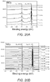
- FIGS. 20A, 20B, and 20C High-resolution XPS multiplex of nickel 2p region of A) 18 nm and B) 60 nm thick nickel film grown on platinum, at 180° C., using Ni( tBu2 DAD) 2 and tert-butyl amine; C) reference nickel film.
- FIGS. 21A and 21B A) XPS depth profile and B) elemental compositions of an 18 nm thick nickel film grown on platinum at 180° C. using Ni( tBu2 DAD) 2 and tert-butyl amine.
- FIGS. 22A and 22B A) XPS depth profile and B) elemental compositions of a 60 nm thick nickel film grown on platinum at 180° C. using Ni( tBu2 DAD) 2 and tert-butyl amine.
- FIG. 23 Plot of thickness versus number of cycles for the growth of nickel metal on ruthenium, copper, and platinum substrates at 180° C. using Ni( tBu2 DAD) 2 and tert-butyl amine.
- FIG. 24 EDS of a CDO substrate after 1000 deposition cycles at 180° C.
- R i where i is an integer
- i include hydrogen, alkyl, lower alkyl, C 1-6 alkyl, C 6-10 aryl, or C 6-10 heteroaryl; single letters (e.g., “n” or “o”) are 0, 1, 2, 3, 4, or 5; percent, “parts of,” and ratio values are by weight;
- the term “polymer” includes “oligomer,” “copolymer,” “terpolymer,” and the like; molecular weights provided for any polymers refers to weight average molecular weight unless otherwise indicated;
- the description of a group or class of materials as suitable or preferred for a given purpose in connection with the invention implies that mixtures of any two or more of the members of the group or class are equally suitable or preferred; description of constituents in chemical terms refers to the constituents at the time of addition to any combination specified in the description, and does not necessarily preclude chemical interactions among the constituents of a mixture once mixed;
- the first definition of an acronym or other abbreviation applies to all subsequent uses here
- alkyl refers to C 1-20 inclusive, linear (i.e., “straight-chain”), branched, saturated or at least partially and in some cases fully unsaturated (i.e., alkenyl and alkynyl) hydrocarbon chains, including for example, methyl, ethyl, n-propyl, isopropyl, butyl, isobutyl, tert-butyl, pentyl, hexyl, octyl, ethenyl, propenyl, butenyl, pentenyl, hexenyl, octenyl, butadienyl, propynyl, butynyl, pentynyl, hexynyl, heptynyl, and allenyl groups.
- Branched refers to an alkyl group in which a lower alkyl group, such as methyl, ethyl or propyl, is attached to a linear alkyl chain.
- Lower alkyl refers to an alkyl group having 1 to about 8 carbon atoms (i.e., a C 1-8 alkyl), e.g., 1, 2, 3, 4, 5, 6, 7, or 8 carbon atoms.
- “Higher alkyl” refers to an alkyl group having about 10 to about 20 carbon atoms, e.g., 10, 11, 12, 13, 14, 15, 16, 17, 18, 19, or 20 carbon atoms.
- transition metal as used herein means an element whose atom has an incomplete d sub-shell, or which can give rise to cations with an incomplete d sub-shell.
- thin film means a coating on a substrate having a thickness less than about 0.5 microns. Typically, a thin film as used herein is a coating with a thickness less than about 500 nm. However, for many applications, a thin film as deposited by ALD is less than about 100 nm.
- thick film as used herein means a coating on a substrate having a thickness greater than about 0.5 microns. Typically, a thick film is deposited by a chemical vapor deposition process (CVD).
- CVD chemical vapor deposition process
- coating means a thin or thick film. Sometimes the term “film” will be used to refer to a coating.
- a method for depositing a coating e.g., a thin film or thick film
- the method includes a step of reacting a vapor of a metal-containing compound described by any of formulae I, II, III, and IV with a Lewis base and in particular, a neutral Lewis base to form a metal coating on the substrate.
- a reducing agent such as molecular hydrogen in added to the Lewis base.
- CVD chemical vapor deposition process
- the reducing agent e.g., molecular hydrogen
- the method is found to selectively deposit a metal layer on metal substrates or the metal component of heterogeneous substrates.
- a metal layer e.g., thin or thick film metal layers (e.g., Co) are deposited on metal substrates or components such as platinum, copper, ruthenium, and the like.
- the metal-containing compound described by any of formulae I, II, III, and IV have a metal atom bonded to a diazadienyl ligand(s).
- the metal coating includes metal atoms in the zero-oxidation state.
- the coating can be a thick film or a thin film.
- the method is a CVD process.
- the method is an ALD process.
- the metal-containing compound i.e., diazadiene complexes
- radicals e.g., diradicals
- the metal-containing compound having formula I will include various forms.
- the metal-containing compound having formula I includes the complex having formula II described as follows: M m [R 1 —NC(R 2 )C(R 3 )N—R 1 ] q II wherein
- M is a transition metal, a group 1 metal, a group 2 metal, Zn, or Cd;
- the metal-containing compound having formula I includes the complex having formula III described as follows:
- the metal-containing compound having formula I includes the complex having formula IV described as follows:
- the methods call for a Lewis base, and in particular, a neutral Lewis base.
- the Lewis base is ammonia or alkyl amine described by the following formula:
- R 5 , R 6 are each independently H or an alkyl.
- R 5 is H or a lower alkyl and R 6 is a lower alkyl.
- R 5 is H or a C 1-6 alkyl and R 6 is a C 1-6 alkyl.
- R 5 and R 6 can be the same or different alkyl groups. Therefore, the alkyl amine can be a primary or secondary amine.
- Examples of specific primary or secondary alkyl amines that can be used include, but are not limited to, methyl amine, ethyl amine, n-propyl amine, isopropyl amine, n-butyl amine, sec-butyl amine, iso-butyl amine, tert-butyl amine, dimethyl amine, diethyl amine, di-n-propyl amine, di-iso-propyl amine, and the like.
- the Lewis base is selected from the group consisting of CO, R 7 NC (isonitriles), phosphines P(R 8 ) 3 , or organophosphites P(OR 9 ) 3 , R 7 , R 8 , and R 9 are each independently H, C 1-6 alkyl or C 6-12 aryl.
- ALD deposition system 10 includes reaction chamber 12 , substrate holder 14 , and vacuum pump 16 .
- the substrate is heated via heater 18 .
- any substrate may be coated as is well known by one skilled in the art of ALD.
- the method of this variation is found to selectively deposit a metal layer on metal substrates or the metal component of heterogeneous substrates.
- metal substrates or components such as platinum, copper, ruthenium, and the like.
- metal layers are not deposited on non-metallic substrates or components such as silicon dioxide, silicon, carbon doped oxide (CDO), and the like.
- the method has a deposition cycle comprising contacting substrate 20 with a vapor of a metal-containing compound described by any of formulae I, II, III, and IV as set forth above.
- the compounds having formulae I, II, III, and IV are activated via a plasma prior to contacting the substrate.
- the vapor is introduced from precursor source 22 into reaction chamber 12 for a first predetermined pulse time.
- the first pulse time is controlled via control valve 24 .
- At least a portion of the vapor of the metal-containing compound modifies (e.g., adsorbs or reacts with) substrate surface 26 to form a modified surface.
- the method further comprises contacting the modified surface with a vapor of Lewis base and in particular, a neutral Lewis base source 30 for a second predetermined pulse time.
- a reducing agent such as molecular hydrogen is combined with the Lewis base prior to introduction into reaction chamber 12 (i.e., prior to contacting the modified surface).
- the reducing agent can be added into the reaction chamber through a separate line.
- the Lewis base e.g., molecular hydrogen
- the Lewis base is present in an amount from about 0.1 to 20 weight percent of the combined weight of the reducing agent and the Lewis base.
- the second predetermined pulse time is controlled via control valve 32 .
- the alkyl amine causes the metal-containing compound to react and form at least a portion of the coating (e.g., thin film) on the surface of the substrate.
- the reduced pressure of chamber 12 is maintained by vacuum pump 16 .
- the method further comprises removing at least a portion of the vapor of the metal containing compound that is lingering in the gas phase (i.e., has not adsorbed or reacted with the substrate) from the vicinity of the substrate before introducing the Lewis base and removing at least a portion of the vapor of the Lewis base from the vicinity of the substrate.
- the metal-containing compound and the Lewis base are removed in purging steps by introducing a purge gas from purge source 34 into reaction chamber 12 for a predetermined purge time.
- the purge time is controlled by control valve 36 .
- the method further includes at least one additional deposition cycle comprising sequentially contacting the substrate with the vapor of a metal-containing compound (formulae I, II, III, and IV) and then the vapor of the Lewis base.
- the substrate is contacted for a plurality of additional deposition cycles.
- the substrate may be contacted with from 1 to several thousand deposition cycles (e.g., 1 to 1000, 1 to 2000, 1 to 3000, 1 to 5000, 500 to 1000, 500 to 2000, 500 to 3000, 500 to 5000 deposition cycles) depending on the thickness of the coating desired.
- the substrate temperature will be at a temperature suitable to the properties of the chemical precursor(s) and film to be formed.
- the substrate is set to a temperature from about 0 to 1000° C.
- the substrate has a temperature from about 50 to 450° C.
- the substrate has a temperature from about 100 to 250° C.
- the substrate has a temperature from about 150 to 400° C.
- the substrate has a temperature from about 200 to 300° C.
- the pressure during film formation is set at a value suitable to the properties of the chemical precursors and film to be formed.
- the pressure is from about 10 ⁇ 6 Torr to about 760 Torr.
- the pressure is from about 5 to about 30 Torr.
- the pressure is from about 1 to about 100 millitorr.
- the pressure is from about 1 to 20 millitorr.
- Pulse times and purge times also depend on the properties of the chemical precursors and the geometric shape of the substrates. Thin film growth on flat substrates uses short pulse and purge times, but pulse and purge times in ALD growth on 3-dimensional substrates can be very long. Therefore, in one refinement, pulse times and purge times are each independently from about 0.0001 to 200 seconds. In another refinement, pulse and purge times are each independently from about 0.1 to about 10 seconds.
- R 1 is C 1-12 alkyl, amine, C 1-12 alkylamino C 6-18 aryl, or Si(R 4 ) 3 .
- R 1 is a lower alkyl.
- R 1 is C 1-4 alkyl.
- Specific examples for R 1 include, but are not limited to, methyl, ethyl, n-propyl, isopropyl n-butyl, sec-butyl, isobutyl, tert-butyl, and the like.
- R 1 is tert-butyl.
- R 1 is C 6-10 aryl.
- R 1 examples include, but are not limited to, phenyl, biphenyl, napthyl, and the like.
- R 1 examples include substituted variations of such groups.
- substituents include, but are not limited to, halogen, hydroxyl, —NO 2 , and in the case of aryl, C 1-4 alkyl. These substituents are particularly relevant when R 1 is aryl.
- R 2 , R 3 are each independently H, C 1-12 alkyl, C 1-12 alkylamino or C 6-18 aryl.
- R 2 , R 3 are each independently H or C 1-4 alkyl.
- specific examples for R 2 , R 3 include, but are not limited to, methyl, ethyl, n-propyl, isopropyl n-butyl, sec-butyl, isobutyl, tert-butyl, and the like.
- R 2 or R 3 is C 1-12 alkylamino or C 2-22 dialkylamino
- the alkyl component is the same as set forth for when R 2 is H or a C 1-12 alkyl. Therefore, additional specific examples for R 2 , R 3 include, but are not limited to, methylamino, ethylamino, propylamino, diethylamino, dimethylamino, dipropylamino, and the like.
- R 2 , R 3 are each independently H or C 6-10 aryl.
- specific examples for R 2 , R 3 include, but are not limited to, phenyl, biphenyl, napthyl, and the like.
- R 2 , R 3 include substituted variations of such groups.
- substituents include, but are not limited to, halogen, hydroxyl, —NO 2 , and in the case of aryl, C 1-4 alkyl.
- M is a metal in a 0, 1+, 2+, or 3+ oxidation state.
- useful transition metals for M include, but are not limited to, Cu, Ni, Co, Cr, Mn, Fe, W, Mo, Ti, Zr, Hf, Rf, V, Nb, Ta, Re, Ru, Rh, Ir, Pd, Pt, and Au.
- Particularly useful examples for M include, but are not limited to, Cr(II), Mn(II), Fe(II), Co(II), and Ni(II).
- M is a transition metal selected from groups 3-7 of the periodic table.
- M can also be Li, Na, K, Rb, Cs, Mg, Ca, Sr, Ba, Zn, Cd and the like.
- the growth of metallic cobalt was demonstrated on a variety of substrates using Co( tBu2 DAD) 2 and tert-butyl amine as precursors ( FIG. 2 ).
- a growth rate of 0.98 ⁇ /cycle was achieved in the ALD window of 170-200° C.
- the resultant films were continuous, featured high-purity metallic cobalt films, and exhibited low resistivity values when grown on metallic substrates.
- XRD X-ray diffraction
- AFM was performed to examine the surface topologies of films of different thicknesses ( ⁇ 10 nm, 100 cycles and ⁇ 100 nm, 1000 cycles) grown on platinum substrates.
- the uncoated platinum substrate has been previously measured to have an rms roughness value of 0.19 nm. (Kerrigan, M. M.; Klesko, J. P.; Rupich, S. M.; Dezelah, C. L.; Kanjolia, R. K.; Chabal, Y. J.; Winter, C. H. J. Chem. Phys. 2017, 146, 052813).
- the ⁇ 10 nm thick film had an rms roughness value of 0.22 nm over the full 5 ⁇ 5 ⁇ m 2 area, which corresponds to 2.2% of the total film thickness.
- the ⁇ 100 nm thick film had an rms roughness value of 3.07 nm over the full 5 ⁇ 5 ⁇ m 2 area, which corresponds to 3.07% of the total film thickness.
- XPS X-ray photoelectron spectroscopy
- binding energies are consistent with values obtained from a cobalt metal standard (Co 2p 3/2 778.11 eV and Co 2p 1/2 793.15 eV) ( FIG. 8C ).
- XPS depth profiling was performed to assess the elemental composition of the films, which revealed >98% pure cobalt metal upon sputtering, with trace impurities ( ⁇ 1% each) of carbon, oxygen, and nitrogen ( FIG. 9 ). After 10 minutes of sputtering, of platinum and cobalt is observed, which may correspond to the formation of an interfacial alloy.
- Cobalt metal films on platinum substrates after 100 cycles ( ⁇ 10 nm thick) and 1000 cycles ( ⁇ 100 nm) were analyzed by AFM, with respective rms surface roughnesses of 0.22 nm (2.2% of total thickness), and 3.07 nm (3.1% of total thickness).
- the rms roughness values show that these films are smooth and continuous over a wide range of thicknesses. XPS analyses reveal that this process deposits high-purity cobalt metal.
- a Picosun R-75BE ALD reactor was used for the thin film deposition experiments.
- Ultra-high purity nitrogen (99.999%, purchased from Airgas) was used as the carrier and purge gas for all depositions, except for the depositions performed to assess the effect of the purity of the carrier gas.
- Nitrogen ( ⁇ 99.999%) was used as both the carrier and purge gas and was purified from ambient air using a Texol GeniSys nitroGenerator, for experiments assessing the effect of the purity of the carrier gas.
- the ALD reactor had a constant flow of the same ultra-high purity nitrogen in the deposition chamber for all depositions, with a pressure of 6-9 Torr.
- the low-temperature ALD of metallic cobalt thin films was performed using Co( tBu2 DAD) 2 and tert-butyl amine as precursors.
- Co( tBu2 DAD) 2 was prepared according to a literature procedure. (Knisley, T. J.; Saly, M. J.; Heeg, M. J.; Roberts, J. L.; Winter, C. H. Organometallics 2011, 30, 5010-5017). All alkyl amines used in depositions (tert-butyl amine, diethyl amine, and trimethylamine) were purchased from Sigma Aldrich. In initial growth trials, the source temperature for Co( tBu2 DAD) 2 was found to be optimum at 130° C.
- ALD growth studies were performed on Ru (13 nm)/TaN (2 nm)/SiO 2 (100 nm)/Si(100), Cu (33 nm)/TaN (7 nm)/SiO 2 (100 nm)/Si(100), Pt (10 nm)/SiO 2 (100 nm)/Si(100), Si(100) with native oxide, Si—H, thermal SiO 2 (100 nm)/Si(100), and CDO ( ⁇ 40 nm)/SiO 2 (100 nm)/Si(100) substrates.
- Si—H substrates were prepared by treating Si(100) with native oxide substrates with a 2% aqueous HF solution, followed by rinsing with deionized water and then drying with a stream of clean, dry air.
- the other substrates were used as received, except that they were rinsed sequentially with isopropanol and deionized water and then were dried with a stream of clean, dry air.
- Film thicknesses were determined using cross-sectional SEM collected on a JEOL-6510LV electron microscope. The growth rates were determined by dividing the measured film thicknesses by the number of deposition cycles. Film thicknesses were measured at a minimum of three positions on each film to evaluate the uniformity.
- EDS was carried out on the JEOL-6510LV electron microscope using an Ametek EDAX system with Genesis Spectrum software. The accelerating voltage for the EDS measurements was 6 kV.
- AFM measurements were conducted using a Bruker BioScope Catalyst AFM using contact mode.
- XPS measurements were conducted using an Al K ⁇ (1486.6 eV) X-ray source at a chamber base pressure of 10 ⁇ 10 Torr.
- Spectra were recorded using a 16-channel detector with a hemispherical analyzer. Sputtering was performed using argon ions supplied by an argon sputter gun positioned at a 45° angle with respect to the substrate normal. Each sample was sputtered over a 2 ⁇ 2 mm 2 area and measured over a 0.8 ⁇ 0.8 mm 2 area. Cobalt metal standards were sputtered with 5 keV argon ions. An uncoated platinum substrate (Pt (10 nm)/SiO 2 (100 nm)/Si(100)) was used as a standard for platinum and was sputtered with 3 keV argon ions.
- the ALD-grown cobalt films on platinum were sputtered with 3 keV argon ions.
- Sheet resistivity measurements were obtained using a Jandel 4-point probe in combination with a Keithley 2400 SourceMeter and a Keithley 2182A Nanovoltmeter. All films grown on metal substrates passed the Scotch tape test.
- the growth of metallic nickel was demonstrated on a variety of substrates using Ni( tBu2 DAD) 2 and tert-butyl amine as precursors ( FIG. 14 ).
- Ni( tBu2 DAD) 2 and tert-butyl amine as precursors ( FIG. 14 ).
- tert-butyl amine a growth rate of 0.60 ⁇ /cycle was achieved in the ALD window of 180-195° C.
- the resultant films were continuous, featured high-purity metallic nickel films, and exhibited low resistivity values when grown on metallic substrates.
- XRD X-ray diffraction
- AFM was performed to examine the surface topologies of nickel films of different thicknesses ( ⁇ 18 nm and ⁇ 60 nm) grown on platinum substrates.
- the uncoated platinum substrate has been previously measured to have an rms roughness value of 0.19 nm. (Kerrigan, M. M.; Klesko, J. P.; Rupich, S. M.; Dezelah, C. L.; Kanjolia, R. K.; Chabal, Y. J.; Winter, C. H. J. Chem. Phys. 2017, 146, 052813).
- the ⁇ 18 nm thick film had an rms roughness value of 0.45 nm over the full 5 ⁇ 5 ⁇ m 2 area, which corresponds to 2.5% of the total film thickness.
- the ⁇ 60 nm thick film had an rms roughness value of 1.52 nm over the full 5 ⁇ 5 ⁇ m 2 area, which corresponds to 2.5% of the total film thickness.
- XPS depth profiling was performed to assess the elemental composition of the films.
- the ⁇ 18 nm thick film was analyzed to assess whether intermixing of the nickel film and platinum substrate occurred. Significant amounts of platinum (>10%) were observed immediately upon sputtering for 0.5 min ( FIG. 21 ).
- the ⁇ 60 nm thick film was analyzed to assess purity of the deposited films, which revealed >97% pure nickel metal upon sputtering, with trace impurities ( ⁇ 1%) of carbon, oxygen, and nitrogen ( FIG. 22 ).
- the resistivities of nickel films grown on ruthenium at the early stages of growth match that of the bare ruthenium substrate, indicating the absence of nickel metal. SEM images also support that no film growth is observed at less than 250 cycles. The delay in growth on ruthenium is likely due to surface oxidation of the ruthenium (vide supra).
- the resistivity of the nickel films on ruthenium after 1000 cycles is 30.6 ⁇ cm, which is comparable to the nickel films grown on platinum of similar thickness (31.8 ⁇ cm). The comparable resistivities suggest that the nickel films grown after 1000 cycles on ruthenium are similar in quality to the films grown on platinum.
- the resistivity measured for nickel metal films grown on copper after 1000 cycles is 22.9 ⁇ cm, which is within experimental error of nickel films of similar thickness grown on platinum. Low resistivities are observed for nickel films grown on copper from 150-500 cycles as well ( ⁇ 27-37 ⁇ cm). After 50 growth cycles, the resistivity of the ⁇ 8 nm thick nickel film grown on copper is that of the copper substrate (1.7 ⁇ cm), which is consistent with the conduction occurring through the lower resistivity copper substrate. It is also possible that intermixing of the nickel and copper layers occur, which will be further investigated with XPS.
- Ni( tBu2 DAD) 2 and tert-butyl amine as precursors. These experiments used a previously established saturative pulsing sequence of Ni( tBu2 DAD) 2 (5.0 s), purge (10.0 s), tert-butyl amine (0.2 s), purge (10.0 s) for 50-1000 cycles. The absence of cobalt metal films on these substrates up to 1000 cycles was confirmed by cross-sectional SEM and EDS ( FIG. 24 ).
- Ni( tBu2 DAD) 2 and tert-butyl amine at 180° C. was demonstrated.
- a linear growth rate of 0.60 ⁇ /cycle from 50-1000 cycles was observed for plots of thickness as a function of the number of cycles.
- the y-intercept for this graph is within experimental error of zero, indicating no nucleation delay, with normal growth observed for as little as 3 nm of nickel on platinum substrates.
- Growth on ruthenium substrates showed a delay of 250 cycles before growth was observed, and is likely due to surface oxidation of the ruthenium substrate.
- a Picosun R-75BE ALD reactor was used for the thin film deposition experiments.
- Ultra-high purity nitrogen (99.999%, purchased from Airgas) was used as the carrier and purge gas for all depositions.
- the ALD reactor had a constant flow of the same ultra-high purity nitrogen in the deposition chamber for all depositions, with a pressure of 6-9 Torr.
- the low-temperature ALD of metallic nickel thin films was performed using Ni( tBu2 DAD) 2 and tert-butyl amine as precursors.
- Ni( tBu2 DAD) 2 was according to a literature procedure. (Knisley, T. J.; Saly, M. J.; Heeg, M. J.; Roberts, J. L.; Winter, C. H.
- ALD growth studies were performed on Ru (13 nm)/TaN (2 nm)/SiO 2 (100 nm)/Si(100), Cu (33 nm)/TaN (7 nm)/SiO 2 (100 nm)/Si(100), Pt (10 nm)/SiO 2 (100 nm)/Si(100), Si(100) with native oxide, Si—H, thermal SiO 2 (100 nm)/Si(100), and CDO ( ⁇ 40 nm)/SiO 2 (100 nm)/Si(100) substrates.
- Si—H substrates were prepared by treating Si(100) with native oxide substrates with a 2% aqueous HF solution, followed by rinsing with deionized water and then drying with a stream of clean, dry air.
- the other substrates were used as received, except that they were rinsed sequentially with isopropanol and deionized water and then were dried with a stream of clean, dry air.
- Film thicknesses were determined using cross-sectional SEM collected on a JEOL-6510LV electron microscope. The growth rates were determined by dividing the measured film thicknesses by the number of deposition cycles. Film thicknesses were measured at a minimum of three positions on each film to evaluate the uniformity.
- EDS was carried out on the JEOL-6510LV electron microscope using an Ametek EDAX system with Genesis Spectrum software. The accelerating voltage for the EDS measurements was 6 kV.
- AFM measurements were conducted using a Bruker BioScope Catalyst AFM using contact mode.
- XPS measurements were conducted using an Al K ⁇ (1486.6 eV) X-ray source at a chamber base pressure of 10 ⁇ 10 Torr.
- Spectra were recorded using a 16-channel detector with a hemispherical analyzer. Sputtering was performed using argon ions supplied by an argon sputter gun positioned at a 45° angle with respect to the substrate normal. Each sample was sputtered over a 2 ⁇ 2 mm 2 area and measured over a 0.8 ⁇ 0.8 mm 2 area. Nickel metal standards were sputtered with 5 keV argon ions. An uncoated platinum substrate (Pt (10 nm)/SiO 2 (100 nm)/Si(100)) was used as a standard for platinum and was sputtered with 3 keV argon ions.
- the ALD-grown cobalt films on platinum were sputtered with 3 keV argon ions.
- Sheet resistivity measurements were obtained using a Jandel 4-point probe in combination with a Keithley 2400 SourceMeter and a Keithley 2182A Nanovoltmeter. All films grown on metal substrates passed the Scotch tape test.
Landscapes
- Chemical & Material Sciences (AREA)
- General Chemical & Material Sciences (AREA)
- Chemical Kinetics & Catalysis (AREA)
- Engineering & Computer Science (AREA)
- Materials Engineering (AREA)
- Mechanical Engineering (AREA)
- Metallurgy (AREA)
- Organic Chemistry (AREA)
- Electrochemistry (AREA)
- Chemical Vapour Deposition (AREA)
Abstract
Description

or radicals thereof;
wherein:
M is a transition metal, a
m is an integer;
n is the formal charge of M;
o is an integer such that the overall formal charge of the compound having formula I is 0;
p is the formal charge of the ligand within the brackets;
R1 is C1-12 alkyl, amine, C6-18 aryl, or Si(R4)3;
R2, R3 are each independently H, C1-10 alkyl, C6-18 aryl, amino, C1-12 alkylamino, or C2-24 dialkylamino; and
R4 is H, C1-10 alkyl or C6-18 aryl. The modified surface is contacted with a vapor of a Lewis base and in particular, a neutral Lewis base, to form at least a portion of the coating (e.g., a thin film) on the surface of the substrate.

or radicals thereof;
wherein:
M is a transition metal, a
m is an integer;
n is the formal charge of M;
o is an integer such that the overall formal charge of the compound having formula I is 0;
p is the formal charge of the ligand within the brackets;
R1 is C1-12 alkyl, amine, C6-18 aryl, or Si(R4)3;
R2, R3 are each independently H, C1-10 alkyl, C6-18 aryl, amino, C1-12 alkylamino, or C2-24 dialkylamino; and
R4 is H, C1-10 alkyl or C6-18 aryl. Advantageously, the method of the present embodiment can be an ALD process or a CVD process.

or radicals (e.g., diradicals) thereof;
wherein:
-
- M is a transition metal, a
group 1 metal, agroup 2 metal, Zn, or Cd; - m is an integer (typically, m is 1);
- n is the formal charge of M (typically, n is 0, 1+, 2+, or 3+);
- o is an integer such that the overall formal charge of the compound having formula I is 0 (typically, o is 1, 2, or 3);
- p is the formal charge of the ligand within the brackets (typically, 0, 1-, or 2-);
- R1 is C1-12 alkyl, amine, C6-18 aryl, or Si(R4)3;
- R2, R3 are each independently H, C1-10 alkyl, C6-18 aryl, amino, C1-12 alkylamino, or C2-24 dialkylamino; and
- R4 is C1-10 alkyl or C6-18 aryl. In a refinement, R1 is a lower alkyl.
- M is a transition metal, a
Mm[R1—NC(R2)C(R3)N—R1]q II
wherein
-
- m is an integer (typically, m is 1);
- q is an integer such that the overall formal charge of the compound having formula II is 0 (typically, q is 1, 2, or 3);
- R1 is C1-12 alkyl, amine, C6-18 aryl, or Si(R4)3;
- R2, R3 are each independently H, C1-10 alkyl, C6-18 aryl, amino, C1-12 alkylamino, or C2-24 dialkylamino; and
- R4 is C1-10 alkyl or C6-18 aryl. In a refinement, R1 is a lower alkyl.

fix per above
wherein
-
- M is a transition metal, a
group 1 metal, agroup 2 metal, Zn, or Cd; - R1 is C1-12 alkyl, amine, C6-18 aryl, or Si(R4)3;
- R2, R3 are each independently H, C1-10 alkyl, C6-18 aryl, amino, C1-12 alkylamino, or C2-24 dialkylamino; and
- R4 is C1-10 alkyl or C6-18 aryl. In a refinement, R1 is a lower alkyl.
- M is a transition metal, a
wherein R5, R6 are each independently H or an alkyl. In a refinement, R5 is H or a lower alkyl and R6 is a lower alkyl. In a further refinement, R5 is H or a C1-6 alkyl and R6 is a C1-6 alkyl. It should be appreciated that R5 and R6 can be the same or different alkyl groups. Therefore, the alkyl amine can be a primary or secondary amine. Examples of specific primary or secondary alkyl amines that can be used include, but are not limited to, methyl amine, ethyl amine, n-propyl amine, isopropyl amine, n-butyl amine, sec-butyl amine, iso-butyl amine, tert-butyl amine, dimethyl amine, diethyl amine, di-n-propyl amine, di-iso-propyl amine, and the like. In other variations, the Lewis base is selected from the group consisting of CO, R7NC (isonitriles), phosphines P(R8)3, or organophosphites P(OR9)3, R7, R8, and R9 are each independently H, C1-6 alkyl or C6-12 aryl.
| TABLE 1 |
| Resistivities of cobalt films grown on metallic substrates |
| using Co(tBu2DAD)2 and tert-butyl amine. |
| Cycles | Rutheniuma,b | Coppera,c | Platinuma,d | ||
| 25 | 55.8 | 1.7 | 46.9 | ||
| 50 | 55.4 | 1.7 | 44.7 | ||
| 100 | 48.6 | 2.3 | 36.8 | ||
| 200 | 19.1 | 13.9 | 18.9 | ||
| 500 | 15.5 | 14.4 | 14.2 | ||
| aValues are in μΩ cm. | |||||
| bThe measured resistivity of the uncoated ruthenium substrate is 52.1 μΩ cm. | |||||
| cThe measured resistivity of the uncoated copper substrate is 1.7 μΩ cm. | |||||
| dThe measured resistivity of the uncoated platinum substrate is 42.6 μΩ cm. | |||||
| TABLE 2 |
| Resistivities of nickel films grown on metallic substrates |
| using Ni(tBu2DAD)2 and tert-butyl amine at 180° C. |
| Cycles | Rutheniuma,b | Coppera,c | Platinuma,d | ||
| 50 | 53.0 | 1.7 | 44.8 | ||
| 150 | 52.8 | 36.7 | 38.6 | ||
| 250 | 51.1 | 34.2 | 36.8 | ||
| 500 | 49.4 | 26.7 | 31.8 | ||
| 1000 | 30.6 | 22.9 | 22.1 | ||
| aValues are in μΩ cm. | |||||
| bThe measured resistivity of the uncoated ruthenium substrate is 52.1 μΩ cm. | |||||
| cThe measured resistivity of the uncoated copper substrate is 1.7 μΩ cm. | |||||
| dThe measured resistivity of the uncoated platinum substrate is 42.6 μΩ cm. | |||||
Claims (32)


Priority Applications (1)
| Application Number | Priority Date | Filing Date | Title |
|---|---|---|---|
| US16/307,608 US11015241B2 (en) | 2016-06-06 | 2017-06-06 | Reaction of diazadiene complexes with amines |
Applications Claiming Priority (3)
| Application Number | Priority Date | Filing Date | Title |
|---|---|---|---|
| US201662345937P | 2016-06-06 | 2016-06-06 | |
| PCT/US2017/036069 WO2017214088A1 (en) | 2016-06-06 | 2017-06-06 | Reaction of diazadiene complexes with amines |
| US16/307,608 US11015241B2 (en) | 2016-06-06 | 2017-06-06 | Reaction of diazadiene complexes with amines |
Publications (2)
| Publication Number | Publication Date |
|---|---|
| US20190301010A1 US20190301010A1 (en) | 2019-10-03 |
| US11015241B2 true US11015241B2 (en) | 2021-05-25 |
Family
ID=60578079
Family Applications (1)
| Application Number | Title | Priority Date | Filing Date |
|---|---|---|---|
| US16/307,608 Active 2037-11-12 US11015241B2 (en) | 2016-06-06 | 2017-06-06 | Reaction of diazadiene complexes with amines |
Country Status (6)
| Country | Link |
|---|---|
| US (1) | US11015241B2 (en) |
| EP (1) | EP3464676B1 (en) |
| KR (1) | KR102467887B1 (en) |
| CN (1) | CN109563621B (en) |
| TW (1) | TWI736631B (en) |
| WO (1) | WO2017214088A1 (en) |
Families Citing this family (18)
| Publication number | Priority date | Publication date | Assignee | Title |
|---|---|---|---|---|
| US10573522B2 (en) | 2016-08-16 | 2020-02-25 | Lam Research Corporation | Method for preventing line bending during metal fill process |
| US10106893B1 (en) | 2017-04-07 | 2018-10-23 | Applied Materials, Inc. | Iridium precursors for ALD and CVD thin film deposition and uses thereof |
| US11440929B2 (en) * | 2018-06-19 | 2022-09-13 | Versum Materials Us, Llc | Bis(diazadiene)cobalt compounds, method of making and method of use thereof |
| KR20210081436A (en) | 2018-11-19 | 2021-07-01 | 램 리써치 코포레이션 | Molybdenum Templates for Tungsten |
| TW202028504A (en) * | 2018-12-03 | 2020-08-01 | 德商馬克專利公司 | Method for highly selective deposition of metal films |
| SG11202108217UA (en) | 2019-01-28 | 2021-08-30 | Lam Res Corp | Deposition of metal films |
| WO2020185618A1 (en) * | 2019-03-11 | 2020-09-17 | Lam Research Corporation | Precursors for deposition of molybdenum-containing films |
| WO2021046058A1 (en) | 2019-09-03 | 2021-03-11 | Lam Research Corporation | Molybdenum deposition |
| CN114667600A (en) | 2019-10-15 | 2022-06-24 | 朗姆研究公司 | Molybdenum fill |
| US11854876B2 (en) | 2019-12-20 | 2023-12-26 | Asm Ip Holding B.V. | Systems and methods for cobalt metalization |
| US11459347B2 (en) | 2021-01-12 | 2022-10-04 | Applied Materials, Inc. | Molybdenum(IV) and molybdenum(III) precursors for deposition of molybdenum films |
| US11434254B2 (en) | 2021-01-12 | 2022-09-06 | Applied Materials, Inc. | Dinuclear molybdenum precursors for deposition of molybdenum-containing films |
| US11390638B1 (en) | 2021-01-12 | 2022-07-19 | Applied Materials, Inc. | Molybdenum(VI) precursors for deposition of molybdenum films |
| JP7686761B2 (en) | 2021-02-23 | 2025-06-02 | ラム リサーチ コーポレーション | Deposition of Molybdenum Films on Oxide Surfaces for 3D-NAND |
| WO2022221210A1 (en) | 2021-04-14 | 2022-10-20 | Lam Research Corporation | Deposition of molybdenum |
| US11760768B2 (en) | 2021-04-21 | 2023-09-19 | Applied Materials, Inc. | Molybdenum(0) precursors for deposition of molybdenum films |
| US12588475B2 (en) | 2021-05-14 | 2026-03-24 | Lam Research Corporation | High selectivity doped hardmask films |
| KR20260042244A (en) * | 2023-08-24 | 2026-03-30 | 다이킨 고교 가부시키가이샤 | Method for manufacturing a thin film |
Citations (17)
| Publication number | Priority date | Publication date | Assignee | Title |
|---|---|---|---|---|
| CN1688742A (en) | 2002-08-28 | 2005-10-26 | 微米技术有限公司 | Systems and methods for forming metal oxides using alcohols |
| CN1896079A (en) | 2005-07-15 | 2007-01-17 | H.C.施塔克股份有限公司 | Tantal and vanadium compounds and their use in chemical vapour deposition (CVD) |
| US20090042041A1 (en) | 2005-02-03 | 2009-02-12 | E. I. Dupont De Nemours And Company | Pyrrolyl complexes of copper for copper metal deposition |
| CN101981226A (en) | 2008-03-26 | 2011-02-23 | 乔治洛德方法研究和开发液化空气有限公司 | Deposition of ternary oxide films containing ruthenium and alkaline earth metals |
| US7897259B1 (en) * | 1993-02-16 | 2011-03-01 | Ppg Industries Ohio, Inc. | Compounds and compositions for coating glass with silicon oxide |
| US20130164456A1 (en) * | 2010-08-24 | 2013-06-27 | Wayne State University | Thermally stable volatile precursors |
| CN103298971A (en) | 2010-11-17 | 2013-09-11 | Up化学株式会社 | Diazadiene-based metal compound, method for producing same, and method for forming thin film using same |
| US20130330473A1 (en) | 2012-06-11 | 2013-12-12 | Wayne State University | Atomic Layer Deposition of Transition Metal Thin Films Using Boranes as the Reducing Agent |
| US20140102365A1 (en) | 2010-10-29 | 2014-04-17 | Jeffrey W. Anthis | Nitrogen-Containing Ligands And Their Use In Atomic Layer Deposition Methods |
| US20140242298A1 (en) | 2011-09-27 | 2014-08-28 | American Air Liquide, Inc. | Nickel bis diazabutadiene precursors, their synthesis, and their use for nickel containing films depositions |
| US20140363575A1 (en) | 2013-06-06 | 2014-12-11 | David Thompson | Methods for the Deposition Of Manganese-Containing Films Using Diazabutadiene-Based Precursors |
| WO2014210512A1 (en) | 2013-06-28 | 2014-12-31 | Wayne State University | Bis(trimethylsilyl) six-membered ring systems and related compounds as reducing agents for forming layers on a substrate |
| US20150105573A1 (en) | 2013-10-14 | 2015-04-16 | Patricio E. Romero | Scalable And High Yield Synthesis Of Transition Metal Bis-Diazabutadienes |
| US20150247240A1 (en) * | 2012-09-21 | 2015-09-03 | Wayne State University | Deposition of metal films based upon complementary reactions |
| WO2015190871A1 (en) | 2014-06-13 | 2015-12-17 | Up Chemical Co., Ltd. | Liquid precursor compositions, preparation methods thereof, and methods for forming layer using the composition |
| CN105390438A (en) | 2014-08-21 | 2016-03-09 | 朗姆研究公司 | Method for void-free cobalt gap fill |
| US20160152650A1 (en) * | 2010-08-24 | 2016-06-02 | Wayne State University | Thermally stable volatile precursors |
Family Cites Families (2)
| Publication number | Priority date | Publication date | Assignee | Title |
|---|---|---|---|---|
| JP4980679B2 (en) * | 2005-11-11 | 2012-07-18 | 東ソー株式会社 | Titanium complexes, methods for producing them, titanium-containing thin films, and methods for forming them |
| EP1916253A1 (en) * | 2006-10-26 | 2008-04-30 | L'AIR LIQUIDE, Société Anonyme pour l'Etude et l'Exploitation des Procédés Georges Claude | New group V metal containing precursors and their use for metal containing film deposition |
-
2017
- 2017-06-05 TW TW106118563A patent/TWI736631B/en active
- 2017-06-06 EP EP17810821.3A patent/EP3464676B1/en active Active
- 2017-06-06 US US16/307,608 patent/US11015241B2/en active Active
- 2017-06-06 KR KR1020197000104A patent/KR102467887B1/en active Active
- 2017-06-06 CN CN201780047863.6A patent/CN109563621B/en active Active
- 2017-06-06 WO PCT/US2017/036069 patent/WO2017214088A1/en not_active Ceased
Patent Citations (23)
| Publication number | Priority date | Publication date | Assignee | Title |
|---|---|---|---|---|
| US7897259B1 (en) * | 1993-02-16 | 2011-03-01 | Ppg Industries Ohio, Inc. | Compounds and compositions for coating glass with silicon oxide |
| US7041609B2 (en) | 2002-08-28 | 2006-05-09 | Micron Technology, Inc. | Systems and methods for forming metal oxides using alcohols |
| CN1688742A (en) | 2002-08-28 | 2005-10-26 | 微米技术有限公司 | Systems and methods for forming metal oxides using alcohols |
| US20090042041A1 (en) | 2005-02-03 | 2009-02-12 | E. I. Dupont De Nemours And Company | Pyrrolyl complexes of copper for copper metal deposition |
| US7442407B2 (en) | 2005-07-15 | 2008-10-28 | H.C. Starck Gmbh | Tantalum and niobium compounds and their use for chemical vapour deposition (CVD) |
| CN1896079A (en) | 2005-07-15 | 2007-01-17 | H.C.施塔克股份有限公司 | Tantal and vanadium compounds and their use in chemical vapour deposition (CVD) |
| CN101981226A (en) | 2008-03-26 | 2011-02-23 | 乔治洛德方法研究和开发液化空气有限公司 | Deposition of ternary oxide films containing ruthenium and alkaline earth metals |
| US8092721B2 (en) | 2008-03-26 | 2012-01-10 | L'air Liquide Societe Anonyme Pour L'etude Et L'exploitation Des Procedes Georges Claude | Deposition of ternary oxide films containing ruthenium and alkali earth metals |
| US20130164456A1 (en) * | 2010-08-24 | 2013-06-27 | Wayne State University | Thermally stable volatile precursors |
| US20160152650A1 (en) * | 2010-08-24 | 2016-06-02 | Wayne State University | Thermally stable volatile precursors |
| US20140102365A1 (en) | 2010-10-29 | 2014-04-17 | Jeffrey W. Anthis | Nitrogen-Containing Ligands And Their Use In Atomic Layer Deposition Methods |
| US9353437B2 (en) | 2010-11-17 | 2016-05-31 | Up Chemical Co., Ltd. | Diazadiene-based metal compound, method for preparing same and method for forming a thin film using same |
| CN103298971A (en) | 2010-11-17 | 2013-09-11 | Up化学株式会社 | Diazadiene-based metal compound, method for producing same, and method for forming thin film using same |
| US20140242298A1 (en) | 2011-09-27 | 2014-08-28 | American Air Liquide, Inc. | Nickel bis diazabutadiene precursors, their synthesis, and their use for nickel containing films depositions |
| US20130330473A1 (en) | 2012-06-11 | 2013-12-12 | Wayne State University | Atomic Layer Deposition of Transition Metal Thin Films Using Boranes as the Reducing Agent |
| US20150247240A1 (en) * | 2012-09-21 | 2015-09-03 | Wayne State University | Deposition of metal films based upon complementary reactions |
| US20140363575A1 (en) | 2013-06-06 | 2014-12-11 | David Thompson | Methods for the Deposition Of Manganese-Containing Films Using Diazabutadiene-Based Precursors |
| CN105492656A (en) | 2013-06-28 | 2016-04-13 | 韦恩州立大学 | Bis(trimethylsilyl) six-membered ring systems and related compounds as reducing agents for layer formation on substrates |
| WO2014210512A1 (en) | 2013-06-28 | 2014-12-31 | Wayne State University | Bis(trimethylsilyl) six-membered ring systems and related compounds as reducing agents for forming layers on a substrate |
| US20150105573A1 (en) | 2013-10-14 | 2015-04-16 | Patricio E. Romero | Scalable And High Yield Synthesis Of Transition Metal Bis-Diazabutadienes |
| WO2015190871A1 (en) | 2014-06-13 | 2015-12-17 | Up Chemical Co., Ltd. | Liquid precursor compositions, preparation methods thereof, and methods for forming layer using the composition |
| CN105390438A (en) | 2014-08-21 | 2016-03-09 | 朗姆研究公司 | Method for void-free cobalt gap fill |
| US9349637B2 (en) | 2014-08-21 | 2016-05-24 | Lam Research Corporation | Method for void-free cobalt gap fill |
Non-Patent Citations (8)
| Title |
|---|
| European Extended Search Report dated Nov. 19, 2019 for EP Appn. No. 17810821.3 filed Dec. 10, 2018. |
| International Search Report dated Sep. 11, 2017 for PCT/US2017/036069 filed Jun. 6, 2017, 13 pgs. |
| Klein, Philippe, et al., "Generation of Organozinc Reagents by Nickel Diazadiene Complex Catalyzed Zinc Insertion into Aryl Sulfonates". Chem. Eur. J. 2020, 26, pp. 176-180. DOI: 10.1002/chem.201904545. * |
| Lorenz, Volker, et al., "Diazadiene Complexes of the Heavy Alkaline-Earth Metals Strontium and Barium: Structures and Reactivity". Organometallics 2013, 32, pp. 4636-4642. dx.doi.org/10.1021/om400622d. * |
| Office Action dated Sep. 17, 2020 for Chinese Appn. No. 201780047863.6 and English Translation, 16 pgs. |
| Tom Dieck, Heindirk, et al., "Bis(diazadien)metall(O)-Komplexe, IV. Nickel(O)-bis(chelate) mit aromatischen N-Substituenten/ Bis(diazadiene)metal(O) Complexes, IV. Nickel(O)-bis(chelates) with Aromatic N-Substituents". Zeitschrift für Naturforschung B, vol. 36: Issue 7, pp. 823-832. * |
| Trifonov, A.A., et al., "Synthesis of bis(cyclopentadienyl)diazadiene complexes of ytterbium, An X-ray structural study of the CpzYb(g-q2:q2-But--N=CH--CH=N--But)Li(DME) complex". Russian Chemical Bulletin, vol. 43, No. 1, Jan. 1994, pp. 145-118. * |
| Yang, Xiuxiu, et al., "A low-valent dinuclear ruthenium diazadiene complex catalyzes the oxidation of dihydrogen and reversible hydrogenation of quinones". Chem. Sci., 2019, 10, pp. 1117-1125. DOI: 10.1039/c8sc02864h. * |
Also Published As
| Publication number | Publication date |
|---|---|
| CN109563621B (en) | 2021-07-20 |
| EP3464676A1 (en) | 2019-04-10 |
| EP3464676A4 (en) | 2019-12-25 |
| CN109563621A (en) | 2019-04-02 |
| TW201817907A (en) | 2018-05-16 |
| KR20190006067A (en) | 2019-01-16 |
| US20190301010A1 (en) | 2019-10-03 |
| KR102467887B1 (en) | 2022-11-16 |
| EP3464676B1 (en) | 2023-09-13 |
| TWI736631B (en) | 2021-08-21 |
| WO2017214088A1 (en) | 2017-12-14 |
Similar Documents
| Publication | Publication Date | Title |
|---|---|---|
| US11015241B2 (en) | Reaction of diazadiene complexes with amines | |
| JP7578748B2 (en) | Synthesis and Use of Precursors for ALD of Molybdenum- or Tungsten-Containing Thin Films - Patent application | |
| JP7300032B2 (en) | Deposition of oxide thin films | |
| US12080548B2 (en) | Selective deposition using hydrophobic precursors | |
| Vos et al. | Atomic layer deposition of cobalt using H2-, N2-, and NH3-based plasmas: on the role of the Co-reactant | |
| US10103057B2 (en) | Use of an inhibitor molecule in chemical vapor deposition to afford deposition of copper on a metal substrate with no deposition on adjacent SIO2 substrate | |
| US20060093848A1 (en) | Atomic layer deposition of noble metals | |
| EP3436622B1 (en) | A method for etching a metal surface | |
| Gebhard et al. | An efficient PE-ALD process for TiO 2 thin films employing a new Ti-precursor | |
| EP1939323A1 (en) | Cyclic chemical vapor deposition of metal-silicon containing films | |
| US20120321817A1 (en) | Bis-ketoiminate copper precursors for deposition of copper-containing films | |
| Ten Eyck et al. | Atomic layer deposition of Pd on an oxidized metal substrate | |
| TW201418504A (en) | Methods for producing nickel-containing films | |
| Dezelah et al. | A low valent metalorganic precursor for the growth of tungsten nitride thin films by atomic layer deposition | |
| Dubois et al. | The decomposition of silane and germane on Ni (111): Implications for heterogeneous catalysis | |
| Kalutarage et al. | Manganese precursor selection and the thermal atomic layer deposition of copper/manganese alloy films | |
| Thompson et al. | Vapor phase deposition of copper films with a Cu (I) β-diketiminate precursor | |
| CN113242861A (en) | Cobalt precursor, method of preparing the same, and method of manufacturing thin film using the same | |
| Bakovets et al. | Mechanism of Ni film CVD with a Ni (ktfaa) 2 precursor on a copper substrate | |
| Anacleto et al. | Atomic layer deposition of tantalum nitride based thin films from cyclopentadienyl type precursor | |
| JP7793870B2 (en) | Selective deposition method of thin film using area-selective atomic layer deposition and substrate on which thin film is selectively formed | |
| WO2018129295A1 (en) | Water assisted highly pure ruthenium thin film deposition | |
| JP2024096051A (en) | Methods for forming and using antimony-containing films and related structures - Patents.com | |
| Luo et al. | UHV Surface Chemistry of bis (ethylcyclopentadienyl) ruthenium,(C2H5C5H4) 2Ru on an Oxide Substrate | |
| CN112458432A (en) | Nb growth by atomic layer deposition technologyxMethod for forming C film |
Legal Events
| Date | Code | Title | Description |
|---|---|---|---|
| FEPP | Fee payment procedure |
Free format text: ENTITY STATUS SET TO UNDISCOUNTED (ORIGINAL EVENT CODE: BIG.); ENTITY STATUS OF PATENT OWNER: SMALL ENTITY |
|
| FEPP | Fee payment procedure |
Free format text: ENTITY STATUS SET TO SMALL (ORIGINAL EVENT CODE: SMAL); ENTITY STATUS OF PATENT OWNER: SMALL ENTITY |
|
| STPP | Information on status: patent application and granting procedure in general |
Free format text: DOCKETED NEW CASE - READY FOR EXAMINATION |
|
| AS | Assignment |
Owner name: WAYNE STATE UNIVERSITY, MICHIGAN Free format text: ASSIGNMENT OF ASSIGNORS INTEREST;ASSIGNORS:WINTER, CHARLES H.;KERRIGAN, MARISSA MARIE;SIGNING DATES FROM 20190322 TO 20190822;REEL/FRAME:052850/0042 |
|
| STPP | Information on status: patent application and granting procedure in general |
Free format text: NOTICE OF ALLOWANCE MAILED -- APPLICATION RECEIVED IN OFFICE OF PUBLICATIONS |
|
| STPP | Information on status: patent application and granting procedure in general |
Free format text: AWAITING TC RESP., ISSUE FEE NOT PAID |
|
| STPP | Information on status: patent application and granting procedure in general |
Free format text: NOTICE OF ALLOWANCE MAILED -- APPLICATION RECEIVED IN OFFICE OF PUBLICATIONS |
|
| STPP | Information on status: patent application and granting procedure in general |
Free format text: PUBLICATIONS -- ISSUE FEE PAYMENT RECEIVED |
|
| STPP | Information on status: patent application and granting procedure in general |
Free format text: PUBLICATIONS -- ISSUE FEE PAYMENT VERIFIED |
|
| STCF | Information on status: patent grant |
Free format text: PATENTED CASE |
|
| MAFP | Maintenance fee payment |
Free format text: PAYMENT OF MAINTENANCE FEE, 4TH YR, SMALL ENTITY (ORIGINAL EVENT CODE: M2551); ENTITY STATUS OF PATENT OWNER: SMALL ENTITY Year of fee payment: 4 |