US11011369B2 - Carbon film forming method, carbon film forming apparatus, and storage medium - Google Patents
Carbon film forming method, carbon film forming apparatus, and storage medium Download PDFInfo
- Publication number
- US11011369B2 US11011369B2 US15/601,245 US201715601245A US11011369B2 US 11011369 B2 US11011369 B2 US 11011369B2 US 201715601245 A US201715601245 A US 201715601245A US 11011369 B2 US11011369 B2 US 11011369B2
- Authority
- US
- United States
- Prior art keywords
- gas
- film
- boron
- process chamber
- workpiece
- Prior art date
- Legal status (The legal status is an assumption and is not a legal conclusion. Google has not performed a legal analysis and makes no representation as to the accuracy of the status listed.)
- Active, expires
Links
Images


Classifications
-
- H10P14/6332—
-
- H—ELECTRICITY
- H01—ELECTRIC ELEMENTS
- H01L—SEMICONDUCTOR DEVICES NOT COVERED BY CLASS H10
- H01L21/00—Processes or apparatus adapted for the manufacture or treatment of semiconductor or solid state devices or of parts thereof
- H01L21/02—Manufacture or treatment of semiconductor devices or of parts thereof
- H01L21/02104—Forming layers
- H01L21/02107—Forming insulating materials on a substrate
- H01L21/02109—Forming insulating materials on a substrate characterised by the type of layer, e.g. type of material, porous/non-porous, pre-cursors, mixtures or laminates
- H01L21/02112—Forming insulating materials on a substrate characterised by the type of layer, e.g. type of material, porous/non-porous, pre-cursors, mixtures or laminates characterised by the material of the layer
- H01L21/02115—Forming insulating materials on a substrate characterised by the type of layer, e.g. type of material, porous/non-porous, pre-cursors, mixtures or laminates characterised by the material of the layer the material being carbon, e.g. alpha-C, diamond or hydrogen doped carbon
-
- H10P14/6902—
-
- C—CHEMISTRY; METALLURGY
- C23—COATING METALLIC MATERIAL; COATING MATERIAL WITH METALLIC MATERIAL; CHEMICAL SURFACE TREATMENT; DIFFUSION TREATMENT OF METALLIC MATERIAL; COATING BY VACUUM EVAPORATION, BY SPUTTERING, BY ION IMPLANTATION OR BY CHEMICAL VAPOUR DEPOSITION, IN GENERAL; INHIBITING CORROSION OF METALLIC MATERIAL OR INCRUSTATION IN GENERAL
- C23C—COATING METALLIC MATERIAL; COATING MATERIAL WITH METALLIC MATERIAL; SURFACE TREATMENT OF METALLIC MATERIAL BY DIFFUSION INTO THE SURFACE, BY CHEMICAL CONVERSION OR SUBSTITUTION; COATING BY VACUUM EVAPORATION, BY SPUTTERING, BY ION IMPLANTATION OR BY CHEMICAL VAPOUR DEPOSITION, IN GENERAL
- C23C16/00—Chemical coating by decomposition of gaseous compounds, without leaving reaction products of surface material in the coating, i.e. chemical vapour deposition [CVD] processes
- C23C16/02—Pretreatment of the material to be coated
- C23C16/0209—Pretreatment of the material to be coated by heating
-
- C—CHEMISTRY; METALLURGY
- C23—COATING METALLIC MATERIAL; COATING MATERIAL WITH METALLIC MATERIAL; CHEMICAL SURFACE TREATMENT; DIFFUSION TREATMENT OF METALLIC MATERIAL; COATING BY VACUUM EVAPORATION, BY SPUTTERING, BY ION IMPLANTATION OR BY CHEMICAL VAPOUR DEPOSITION, IN GENERAL; INHIBITING CORROSION OF METALLIC MATERIAL OR INCRUSTATION IN GENERAL
- C23C—COATING METALLIC MATERIAL; COATING MATERIAL WITH METALLIC MATERIAL; SURFACE TREATMENT OF METALLIC MATERIAL BY DIFFUSION INTO THE SURFACE, BY CHEMICAL CONVERSION OR SUBSTITUTION; COATING BY VACUUM EVAPORATION, BY SPUTTERING, BY ION IMPLANTATION OR BY CHEMICAL VAPOUR DEPOSITION, IN GENERAL
- C23C16/00—Chemical coating by decomposition of gaseous compounds, without leaving reaction products of surface material in the coating, i.e. chemical vapour deposition [CVD] processes
- C23C16/02—Pretreatment of the material to be coated
- C23C16/0272—Deposition of sub-layers, e.g. to promote the adhesion of the main coating
-
- C—CHEMISTRY; METALLURGY
- C23—COATING METALLIC MATERIAL; COATING MATERIAL WITH METALLIC MATERIAL; CHEMICAL SURFACE TREATMENT; DIFFUSION TREATMENT OF METALLIC MATERIAL; COATING BY VACUUM EVAPORATION, BY SPUTTERING, BY ION IMPLANTATION OR BY CHEMICAL VAPOUR DEPOSITION, IN GENERAL; INHIBITING CORROSION OF METALLIC MATERIAL OR INCRUSTATION IN GENERAL
- C23C—COATING METALLIC MATERIAL; COATING MATERIAL WITH METALLIC MATERIAL; SURFACE TREATMENT OF METALLIC MATERIAL BY DIFFUSION INTO THE SURFACE, BY CHEMICAL CONVERSION OR SUBSTITUTION; COATING BY VACUUM EVAPORATION, BY SPUTTERING, BY ION IMPLANTATION OR BY CHEMICAL VAPOUR DEPOSITION, IN GENERAL
- C23C16/00—Chemical coating by decomposition of gaseous compounds, without leaving reaction products of surface material in the coating, i.e. chemical vapour deposition [CVD] processes
- C23C16/22—Chemical coating by decomposition of gaseous compounds, without leaving reaction products of surface material in the coating, i.e. chemical vapour deposition [CVD] processes characterised by the deposition of inorganic material, other than metallic material
- C23C16/26—Deposition of carbon only
-
- C—CHEMISTRY; METALLURGY
- C23—COATING METALLIC MATERIAL; COATING MATERIAL WITH METALLIC MATERIAL; CHEMICAL SURFACE TREATMENT; DIFFUSION TREATMENT OF METALLIC MATERIAL; COATING BY VACUUM EVAPORATION, BY SPUTTERING, BY ION IMPLANTATION OR BY CHEMICAL VAPOUR DEPOSITION, IN GENERAL; INHIBITING CORROSION OF METALLIC MATERIAL OR INCRUSTATION IN GENERAL
- C23C—COATING METALLIC MATERIAL; COATING MATERIAL WITH METALLIC MATERIAL; SURFACE TREATMENT OF METALLIC MATERIAL BY DIFFUSION INTO THE SURFACE, BY CHEMICAL CONVERSION OR SUBSTITUTION; COATING BY VACUUM EVAPORATION, BY SPUTTERING, BY ION IMPLANTATION OR BY CHEMICAL VAPOUR DEPOSITION, IN GENERAL
- C23C16/00—Chemical coating by decomposition of gaseous compounds, without leaving reaction products of surface material in the coating, i.e. chemical vapour deposition [CVD] processes
- C23C16/44—Chemical coating by decomposition of gaseous compounds, without leaving reaction products of surface material in the coating, i.e. chemical vapour deposition [CVD] processes characterised by the method of coating
- C23C16/46—Chemical coating by decomposition of gaseous compounds, without leaving reaction products of surface material in the coating, i.e. chemical vapour deposition [CVD] processes characterised by the method of coating characterised by the method used for heating the substrate
-
- C—CHEMISTRY; METALLURGY
- C23—COATING METALLIC MATERIAL; COATING MATERIAL WITH METALLIC MATERIAL; CHEMICAL SURFACE TREATMENT; DIFFUSION TREATMENT OF METALLIC MATERIAL; COATING BY VACUUM EVAPORATION, BY SPUTTERING, BY ION IMPLANTATION OR BY CHEMICAL VAPOUR DEPOSITION, IN GENERAL; INHIBITING CORROSION OF METALLIC MATERIAL OR INCRUSTATION IN GENERAL
- C23C—COATING METALLIC MATERIAL; COATING MATERIAL WITH METALLIC MATERIAL; SURFACE TREATMENT OF METALLIC MATERIAL BY DIFFUSION INTO THE SURFACE, BY CHEMICAL CONVERSION OR SUBSTITUTION; COATING BY VACUUM EVAPORATION, BY SPUTTERING, BY ION IMPLANTATION OR BY CHEMICAL VAPOUR DEPOSITION, IN GENERAL
- C23C16/00—Chemical coating by decomposition of gaseous compounds, without leaving reaction products of surface material in the coating, i.e. chemical vapour deposition [CVD] processes
- C23C16/44—Chemical coating by decomposition of gaseous compounds, without leaving reaction products of surface material in the coating, i.e. chemical vapour deposition [CVD] processes characterised by the method of coating
- C23C16/52—Controlling or regulating the coating process
-
- H—ELECTRICITY
- H01—ELECTRIC ELEMENTS
- H01L—SEMICONDUCTOR DEVICES NOT COVERED BY CLASS H10
- H01L21/00—Processes or apparatus adapted for the manufacture or treatment of semiconductor or solid state devices or of parts thereof
- H01L21/02—Manufacture or treatment of semiconductor devices or of parts thereof
- H01L21/02104—Forming layers
- H01L21/02107—Forming insulating materials on a substrate
- H01L21/02109—Forming insulating materials on a substrate characterised by the type of layer, e.g. type of material, porous/non-porous, pre-cursors, mixtures or laminates
- H01L21/02205—Forming insulating materials on a substrate characterised by the type of layer, e.g. type of material, porous/non-porous, pre-cursors, mixtures or laminates the layer being characterised by the precursor material for deposition
- H01L21/02208—Forming insulating materials on a substrate characterised by the type of layer, e.g. type of material, porous/non-porous, pre-cursors, mixtures or laminates the layer being characterised by the precursor material for deposition the precursor containing a compound comprising Si
- H01L21/02211—Forming insulating materials on a substrate characterised by the type of layer, e.g. type of material, porous/non-porous, pre-cursors, mixtures or laminates the layer being characterised by the precursor material for deposition the precursor containing a compound comprising Si the compound being a silane, e.g. disilane, methylsilane or chlorosilane
-
- H—ELECTRICITY
- H01—ELECTRIC ELEMENTS
- H01L—SEMICONDUCTOR DEVICES NOT COVERED BY CLASS H10
- H01L21/00—Processes or apparatus adapted for the manufacture or treatment of semiconductor or solid state devices or of parts thereof
- H01L21/02—Manufacture or treatment of semiconductor devices or of parts thereof
- H01L21/02104—Forming layers
- H01L21/02107—Forming insulating materials on a substrate
- H01L21/02225—Forming insulating materials on a substrate characterised by the process for the formation of the insulating layer
- H01L21/0226—Forming insulating materials on a substrate characterised by the process for the formation of the insulating layer formation by a deposition process
- H01L21/02263—Forming insulating materials on a substrate characterised by the process for the formation of the insulating layer formation by a deposition process deposition from the gas or vapour phase
- H01L21/02271—Forming insulating materials on a substrate characterised by the process for the formation of the insulating layer formation by a deposition process deposition from the gas or vapour phase deposition by decomposition or reaction of gaseous or vapour phase compounds, i.e. chemical vapour deposition
-
- H—ELECTRICITY
- H01—ELECTRIC ELEMENTS
- H01L—SEMICONDUCTOR DEVICES NOT COVERED BY CLASS H10
- H01L21/00—Processes or apparatus adapted for the manufacture or treatment of semiconductor or solid state devices or of parts thereof
- H01L21/02—Manufacture or treatment of semiconductor devices or of parts thereof
- H01L21/02104—Forming layers
- H01L21/02107—Forming insulating materials on a substrate
- H01L21/02296—Forming insulating materials on a substrate characterised by the treatment performed before or after the formation of the layer
- H01L21/02299—Forming insulating materials on a substrate characterised by the treatment performed before or after the formation of the layer pre-treatment
- H01L21/02304—Forming insulating materials on a substrate characterised by the treatment performed before or after the formation of the layer pre-treatment formation of intermediate layers, e.g. buffer layers, layers to improve adhesion, lattice match or diffusion barriers
-
- H—ELECTRICITY
- H01—ELECTRIC ELEMENTS
- H01L—SEMICONDUCTOR DEVICES NOT COVERED BY CLASS H10
- H01L21/00—Processes or apparatus adapted for the manufacture or treatment of semiconductor or solid state devices or of parts thereof
- H01L21/67—Apparatus specially adapted for handling semiconductor or electric solid state devices during manufacture or treatment thereof; Apparatus specially adapted for handling wafers during manufacture or treatment of semiconductor or electric solid state devices or components ; Apparatus not specifically provided for elsewhere
- H01L21/67005—Apparatus not specifically provided for elsewhere
- H01L21/67011—Apparatus for manufacture or treatment
- H01L21/67098—Apparatus for thermal treatment
-
- H10P14/6334—
-
- H10P14/6506—
-
- H10P14/668—
-
- H10P14/6682—
-
- H10P14/6923—
-
- H10P72/0431—
-
- H10P95/90—
-
- H—ELECTRICITY
- H01—ELECTRIC ELEMENTS
- H01L—SEMICONDUCTOR DEVICES NOT COVERED BY CLASS H10
- H01L21/00—Processes or apparatus adapted for the manufacture or treatment of semiconductor or solid state devices or of parts thereof
- H01L21/67—Apparatus specially adapted for handling semiconductor or electric solid state devices during manufacture or treatment thereof; Apparatus specially adapted for handling wafers during manufacture or treatment of semiconductor or electric solid state devices or components ; Apparatus not specifically provided for elsewhere
- H01L21/67005—Apparatus not specifically provided for elsewhere
- H01L21/67011—Apparatus for manufacture or treatment
- H01L21/67098—Apparatus for thermal treatment
- H01L21/67109—Apparatus for thermal treatment mainly by convection
-
- H10P72/0434—
Definitions
- the present disclosure relates to a carbon film forming method, a carbon film forming apparatus, and a non-transitory computer-readable storage medium.
- Carbon (C) is getting a lot of attentions as one of the materials used in patterning processing of next-generation semiconductor devices. In such a patterning process, a good buriability for a stepped shape is required.
- a plasma CVD method or a thermal CVD method has been generally known as a method of forming a carbon film.
- a film formation temperature may be kept at a low level (in a range of 100 to 500 degrees C. in the related art), but step coverage is poor.
- the plasma CVD method may not be suitable for forming a carbon film on an underlying film having irregularities such as a line pattern, a hole pattern or the like.
- a step coverage is relatively good, but a film formation temperature needs to be kept at a high level (in a range of 800 to 1,000 degrees C. in the related art). Even if film formation conditions are optimized, there is a limit that the film formation temperature falls within a range of 600 to 800 degrees C.
- the thermal CVD method may not be suitable for use in a process applied to an upper layer portion of a semiconductor device.
- a technique which uses a pyrolysis temperature lowering gas that lowers a pyrolysis temperature of a hydrocarbon-based carbon source gas used as a film-forming raw material, when forming a carbon film by a thermal CVD method which provides a relatively good step coverage.
- a technique is to reduce a film formation temperature using a halogen-containing gas such as a Cl 2 gas as the pyrolysis temperature lowering gas, thus lowering the pyrolysis temperature.
- this technique involves forming a seed layer for improving adhesion by supplying an aminosilane-based gas onto an underlying film before forming a carbon film.
- Some embodiments of the present disclosure provide a carbon film forming method and a carbon film forming apparatus, which are capable of forming a carbon film having good adhesion, in a case where a pyrolysis temperature lowering gas is used to perform film formation at a low temperature, and a non-transitory computer-readable storage medium.
- a method of forming a carbon film on a workpiece which includes: loading the workpiece into a process chamber; supplying a gas containing a boron-containing gas into the process chamber to form a seed layer composed of a boron-based thin film on a surface of the workpiece; and subsequently, supplying a hydrocarbon-based carbon source gas and a pyrolysis temperature lowering gas containing a halogen element and which lowers a pyrolysis temperature of the hydrocarbon-based carbon source gas into the process chamber, heating the hydrocarbon-based carbon source gas to a temperature lower than the pyrolysis temperature to pyrolyze the hydrocarbon-based carbon source gas, and forming the carbon film on the workpiece by a thermal CVD.
- an apparatus of forming a carbon film on a workpiece which includes: a process chamber in which the workpiece on which the carbon film is to be formed is accommodated; a process gas supply mechanism configured to supply a gas to be used for process into the process chamber; a heating device configured to heat the workpiece accommodated in the process chamber; a loading mechanism configured to load the workpiece into the process chamber, and a control part configured to control the process gas supply mechanism, the heating device and the loading mechanism to perform the aforementioned method.
- a non-transitory computer-readable storage medium storing a program that operates on a computer for controlling a carbon film forming apparatus, wherein the program, when executed, causes the computer to control the carbon film forming apparatus so as to perform the aforementioned method.
- FIG. 1 is a sectional view schematically showing an example of a film forming apparatus capable of carrying out a film forming method of the present disclosure.
- FIG. 2 is a flowchart showing a flow of a carbon film forming method according to one embodiment of the present disclosure.
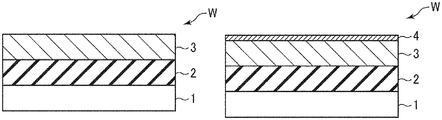
- FIGS. 3A to 3C are process sectional views used to explain the carbon film forming method according to one embodiment of the present disclosure.
- FIGS. 4A and 4B are views used to explain a comparison between a reaction model in which an aminosilane-based seed layer is used as a seed layer and a reaction model in which a boron-based thin film is used as a seed layer.
- FIG. 5 is a view showing results and relevant SEM photographs of tape test of samples A to D in an experimental example.
- the present inventors conducted research over and over to solve the aforementioned problems and, consequently, found the following facts.
- the use of boron or boron nitride as a seed layer makes it possible to suppress the reaction between a pyrolysis temperature lowering gas such as a Cl 2 gas and an underlying layer, thereby preventing deterioration of adhesion to the underlying layer.
- FIG. 1 is a sectional view schematically showing an example of a film forming apparatus capable of carrying out a film forming method of the present disclosure.
- a film forming apparatus 100 is configured as a vertical batch type film forming apparatus and includes a cylindrical outer wall 101 with a ceiling portion and a cylindrical inner wall 102 installed inside the outer wall 101 .
- the outer wall 101 and the inner wall 102 are made of, e.g., quartz.
- An inner region of the inner wall 102 serves as a process chamber S in which a plurality of semiconductor wafers (hereinafter simply referred to as “wafers”) W as workpieces is collectively processed.
- wafers semiconductor wafers
- the outer wall 101 and the inner wall 102 are spaced apart from each other along a horizontal direction with an annular space 104 formed therebetween and are joined to a base member 105 at their respective lower end portions.
- An upper end portion of the inner wall 102 is spaced apart from the ceiling portion of the outer wall 101 such that the upper portion of the process chamber S communicates with the annular space 104 .
- the annular space 104 communicating with the upper portion of the process chamber S serves as an exhaust path.
- a gas supplied and diffused into the process chamber S flows from the lower portion of the process chamber S to the upper portion thereof and is sucked into the annular space 104 .
- An exhaust pipe 106 is connected to the lower end portion of the annular space 104 and is also connected to an exhaust device 107 .
- the exhaust device 107 includes a vacuum pump and the like, exhausts the process chamber S, and adjusts an internal pressure of the process chamber S to a pressure suitable for processing.
- a heating device 108 is installed outside the outer wall 101 so as to surround the process chamber S.
- the heating device 108 adjusts an internal temperature of the process chamber S to a temperature suitable for processing and heats the plurality of wafers W at a time.
- the lower portion of the process chamber S is in communication with an opening 109 formed in the base member 105 .
- a cylindrical manifold 110 made of a material such as stainless steel is coupled to the opening 109 via a seal member 111 such as an O-ring.
- a lower end portion of the manifold 110 is opened such that a boat 112 is inserted into the process chamber S through such an opening.
- the boat 112 is made of, e.g., quartz and includes a plurality of columns 113 . In the columns 113 are formed grooves (not shown) by which a plurality of target substrates is supported at a time.
- the boat 112 can mount the plurality of, e.g., 50 to 150, wafers W as the target substrates, in multiple stages.
- the boat 112 with the plurality of wafers W mounted thereon is loaded into the process chamber S, so that the plurality of wafers W can be accommodated in the process chamber S.
- the boat 112 is placed on a table 115 via a quartz heat-insulating tube 114 .
- the table 115 is supported on a rotary shaft 117 penetrating a lid part 116 made of, e.g., stainless steel.
- the lid part 116 opens and closes the opening of the lower end portion of the manifold 110 .
- a magnetic fluid seal 118 is installed in a penetration portion of the lid part 116 to rotatably support the rotary shaft 117 while hermetically sealing the rotary shaft 117 .
- a seal member 119 such as an O-ring is interposed between a peripheral portion of the lid part 116 and the lower end portion of the manifold 110 to maintain the scalability of the process chamber S.
- the rotary shaft 117 is attached to the tip of an arm 120 supported by an elevating mechanism (not shown) such as a boat elevator.
- an elevating mechanism such as a boat elevator.
- the film forming apparatus 100 includes a processing gas supply mechanism 130 configured to supply a gas used for process into the process chamber S.
- the processing gas supply mechanism 130 of this example includes a hydrocarbon-based carbon source gas supply source 131 a , a pyrolysis temperature lowering gas supply source 131 b , an inert gas supply source 131 c and a seed gas supply source 131 d.
- the hydrocarbon-based carbon source gas supply source 131 a is coupled to a gas supply port 134 a via a mass flow controller (MFC) 132 a and an opening/closing valve 133 a .
- the pyrolysis temperature lowering gas supply source 131 b is coupled to a gas supply port 134 b via a mass flow controller (MFC) 132 b and an opening/closing valve 133 b .
- the inert gas supply source 131 c is coupled to a gas supply port 134 c via a mass flow controller (MFC) 132 c and an opening/closing valve 133 c .
- the seed gas supply source 131 d is coupled to a gas supply port 134 d via a mass flow controller (MFC) 132 d and an opening/closing valve 133 d .
- MFC mass flow controller
- the gas supply ports 134 a to 134 d are respectively installed so as to horizontally penetrate a side wall of the manifold 110 and diffuse gases supplied thereto toward the interior of the process chamber S defined above the manifold 110 .
- a hydrocarbon-based carbon source gas supplied from the hydrocarbon-based carbon source gas supply source 131 a is a gas used to form a carbon film by a thermal CVD method.
- the hydrocarbon-based carbon source gas may be a gas containing hydrocarbon represented by at least one of molecular formulae of C n H 2n+2 , C m H 2m and C m H 2m ⁇ 2 (where, n is the natural number of one or more and m is the natural number of two or more).
- the hydrocarbon-based carbon source gas may include a benzene gas (C 6 H 6 ).
- the hydrocarbon represented by the molecular formula of C n H 2n+2 may include a methane gas (CH 4 ), an ethane gas (C 2 H 6 ), a propane gas (C 3 H 8 ), a butane gas (C 4 H 10 : also containing other isomer), a pentane gas (C 5 H 12 : also containing other isomer) or the like.
- the hydrocarbon represented by the molecular formula of C m H 2m may include an ethylene gas (C 2 H 4 ), a propylene gas (C 3 H 6 : also containing other isomer), a butylene gas (C 4 H 8 : also containing other isomer), a pentene gas (C 5 H 10 : also containing other isomer) or the like.
- the hydrocarbon represented by the molecular formula of C m H 2m ⁇ 2 may include an acetylene gas (C 2 H 2 ), a propyne gas (C 3 H 4 : also containing other isomer), a butadiene gas (C 4 H 6 : also containing other isomer), an isoprene gas (C 5 H 8 : also containing other isomer) or the like.
- a gas containing a halogen element is used as the pyrolysis temperature lowering gas supplied from the pyrolysis temperature lowering gas supply source 131 b .
- the gas containing a halogen element has a function of lowering a pyrolysis temperature of the hydrocarbon-based carbon source gas by its catalytic function to drop a film formation temperature of the carbon film by the thermal CVD method.
- the halogen element includes fluorine (F), chlorine (Cl), bromine (Br) and iodine (I).
- the halogen element-containing gas may be a halogen element alone, that is to say, a single fluorine (F 2 ) gas, a single chlorine (Cl 2 ) gas, a single bromine (Br 2 ) gas or a single iodine (I 2 ) gas, or a compound thereof.
- the halogen element alone has an advantage in that heat for pyrolysis is unnecessary and the effect of lowering the pyrolysis temperature of the hydrocarbon-based carbon source gas is high.
- fluorine having high reactivity may deteriorate surface roughness and flatness of the formed carbon film. Therefore, chlorine, bromine and iodine excluding fluorine may be used as the halogen element. In particular, chlorine is preferable from the viewpoint of handling.
- the inert gas supplied from the inert gas supply source 131 c is used as a purge gas or a dilution gas.
- An example of the inert gas may include a noble gas such as a N 2 gas or an Ar gas.
- the seed gas supplied from the seed gas supply source 131 d is to form a seed layer on the underlying layer for improving the adhesion between the underlying layer and the carbon film, prior to forming the carbon film.
- a boron-based thin film is used as the seed layer. Boron or boron nitride which has a stoichiometric composition or remains in a boron-rich state may be used for the boron-based thin film.
- a gas containing a boron-containing gas is used as the seed gas.
- a borane-based gas typified by a diborane (B 2 H 6 ) gas, or a boron trichloride (BCl 3 ) gas may be used as the boron-containing gas used as the seed gas.
- the B 2 H 6 gas may be more suitably used.
- a nitride gas may be used in addition to the boron-containing gas.
- An ammonia (NH 3 ) gas may be suitably used as the nitriding gas.
- An organic amine gas and a hydrazine gas may also be used as the nitriding gas.
- a separate nitriding gas supply source may be installed to supply the nitriding gas into the process chamber S from a separate gas supply port via a separate mass flow controller (MFC) and a separate opening/closing valve.
- MFC mass flow controller
- the film forming apparatus 100 includes a control part 150 .
- the control part 150 is provided with a process controller 151 composed of a microprocessor (computer), which controls respective components of the filming apparatus 100 .
- a user interface 152 and a storage part 153 are connected to the process controller 151 .
- the user interface 152 includes an input part provided with a touch panel display, a keyboard and the like for allowing an operator to input commands to manage the film forming apparatus 100 , and a display part for visually displaying the operation status of the film forming apparatus 100 .
- the storage part 153 stores a so-called process recipe which includes a control program for realizing various processes executed in the film forming apparatus 100 under the control of the process controller 151 , and a program for causing the respective components of the film forming apparatus 100 to perform processes according to process conditions.
- the process recipe is stored in a storage medium in the storage part 153 .
- the storage medium may be a hard disk or a semiconductor memory, or may be a portable medium such as a CD-ROM, a DVD, a flash memory or the like. Further, the process recipe may be appropriately transmitted from another apparatus, for example, via a dedicated line.
- the process recipe is read out from the storage part 153 according to an operator's instruction or the like provided from the user interface 152 , and the process controller 151 causes the film forming apparatus 100 to execute a process according to the process recipe thus read.
- FIG. 2 is a flowchart showing a flow of the carbon film forming method according to one embodiment of the present disclosure and FIGS. 3A to 3C are process sectional views used to explain the carbon film forming method.
- the wafer boat 112 is inserted into the process chamber S in the film forming apparatus 100 from below. In this way, the plurality of wafers W is loaded into the process chamber S (Step S 1 ).
- Step S 1 the interior of the process chamber S is hermetically sealed. In this state, the interior of the process chamber S is evacuated to maintain a predetermined depressurized atmosphere, power supplied to the heating device 108 is controlled to raise the wafer temperature to a process temperature, and the wafer boat 112 is rotated.
- a gas containing a boron-containing gas is supplied as a seed gas from the seed gas supply source 131 d and is adsorbed onto a wafer surface (surface of the amorphous silicon film 3 as the underlying film) to form a seed layer 4 for improving adhesion (Step S 2 , FIG. 3B ).
- Step S 2 a borane-based gas typified by a diborane (B 2 H 6 ) gas, or a boron trichloride (BCl 3 ) gas is used as the boron-containing gas supplied from the seed gas supply source 131 d to form a boron-based thin film as the seed layer 4 .
- a borane-based gas typified by a diborane (B 2 H 6 ) gas, or a boron trichloride (BCl 3 ) gas is used as the boron-containing gas supplied from the seed gas supply source 131 d to form a boron-based thin film as the seed layer 4 .
- a boron film composed of boron alone, or a boron nitride film which has a stoichiometric composition or remains in a boron-rich state may be suitably used as the boron-based thin film.
- the boron film may be formed by pyrolysis using only the boron-containing gas as the gas containing a boron-containing gas.
- the boron nitride film may be formed using a nitriding gas such as an ammonia (NH 3 ) gas, an organic amine gas, an hydrazine gas or the like, in addition to the boron-containing gas, as the gas containing a boron-containing gas.
- a B 2 H 6 gas may be used as the boron-containing gas
- the NH 3 gas may be used as the nitriding gas.
- the temperature of the wafer W as a workpiece at the time of forming the seed layer 4 in Step S 2 may fall within a range of 200 to 300 degrees C. from the viewpoint of efficient film formation and good controllability.
- Step S 2 After forming the seed layer 4 in Step S 2 , the interior of the process chamber S is purged and a carbon film 5 is formed by thermal CVD without using plasma assist (Step S 3 , FIG. 3C ).
- a gas containing hydrocarbon for example, a C 5 H 8 gas
- a halogen-containing gas for example, a Cl 2 gas
- the hydrocarbon-based carbon source gas is heated to a predetermined temperature lower than the pyrolysis temperature thereof and is pyrolyzed.
- the carbon film 5 is formed on the surface of the wafer W by the thermal CVD.
- the process chamber S is exhausted by the exhaust device 107 .
- a N 2 gas is supplied as a purge gas from the inert gas supply source 131 c into the process chamber S to purge the process chamber S.
- the internal pressure of the process chamber S is returned to atmospheric pressure, and subsequently, the wafer boat 112 is moved down to unload the wafers W.
- the pyrolysis temperature of the hydrocarbon-based carbon source gas is lowered by the catalytic effect thereof, and the carbon film is formed at a temperature lower than the pyrolysis temperature of the carbon source gas. That is to say, a temperature of 650 degrees C. or more (800 to 1,000 degrees C., specifically 650 to 800 degrees C. in the optimal conditions, which are described in the section BACKGROUND of the present disclosure), which was conventionally necessary for forming a carbon film in the thermal CVD method using a hydrocarbon-based carbon source gas, can be lowered to a lower temperature.
- the carbon film can be formed at a low temperature of about 300 degrees C.
- the conventional technique described in the section BACKGROUND of the present disclosure shows the effects of decomposing a hydrocarbon-based carbon source gas (C x H y ), for example, an ethylene gas (C 2 H 4 ), by drawing hydrogen (H) out of the hydrocarbon-based carbon source gas (C x H y ) through the use of a Cl 2 gas as a gas containing a halogen element constituting a pyrolysis temperature lowering gas. That is to say, at the time of forming a carbon film, a halogen element such as chlorine (Cl) draws H on the surface layer and is discharged as, for example, HCl. For this reason, dangling bonds are generated by desorption of H, which contributes to film formation.
- This technique also describes that the adhesion between the underlying film and the carbon film is increased by adsorbing an aminosilane-based gas as a seed layer between the underlying film and the carbon film.
- the boron-based thin film is used as the seed layer 4 , deterioration of adhesion hardly occurs due to a difference in reactivity between the boron-based thin film and the underlying silicon film. That is to say, by using the boron-based thin film as the seed layer 4 , the reactivity with Cl is suppressed, which makes it hard for Cl to terminate the dangling bonds, as shown in FIG. 4B . Therefore, the dangling bond activation sites as carbon adsorption sites are hardly decreased, thereby preventing deterioration of adhesion of the carbon film due to adsorption inhibition. Therefore, it is possible to form a carbon film having good adhesion irrespective of the underlying film.
- a thickness of the boron-based thin film constituting the seed layer 4 may fall within a range of 0.5 to 3.0 nm.
- Film formation temperature 200 to 300 degrees C.
- Film formation temperature 300 to 600 degrees C. (more specifically, 350 to 400 degrees C.)
- Nitriding gas NH 3
- Thickness of seed layer 1.0 nm
- Hydrocarbon-based carbon source gas butadiene (C 4 H 6 )
- the structure of the workpiece is not limited thereto.
- Sample A to D were obtained by forming a thermal oxide film (Th-Ox), an amorphous silicon film (a-Si), a boron silicon film (BSiLT) and a SiN film (SiN) as underlying films on bare silicon wafers, respectively; forming a boron nitride film as a seed layer on each of the underlying films thus formed; and forming amorphous carbons film using butadiene (C 4 H 6 ) as a hydrocarbon-based carbon source gas and a Cl 2 gas as a pyrolysis temperature lowering gas, respectively.
- a thermal oxide film Thi-Ox
- a-Si amorphous silicon film
- BSiLT boron silicon film
- SiN SiN film
- Sample E was obtained by forming a seed layer on a bare silicon wafer directly using an aminosilane-based gas and subsequently; forming an amorphous carbon film on the seed layer as in the above.
- Sample F was obtained by forming a SiO 2 film as an underlying film, forming a seed layer on the SiO 2 film using an aminosilane-based gas, and subsequently; forming an amorphous carbon film on the seed layer as in the above.
- the film formation conditions for the amorphous carbon film are as follows for all samples.
- Thickness of seed layer less than 1 nm
- BTBAS bis-tertiary-butylaminosilane
- Process temperature 400 degrees C.
- the tape test was conducted under the conditions of JIS K 5600-5-6 (cross-cut method) and was evaluated based on the presence or absence of film peeling.
- Sample E the silicon wafer was damaged by an etching reaction and was subjected to no tape test.
- Sample F received a not good (NG) decision in the tape test.
- a workpiece has been illustrated with a semiconductor wafer in the above embodiment, the present disclosure is not limited to the semiconductor wafer.
- the present disclosure may be applied to another workpiece such as a glass substrate used for an FPD (Flat Panel Display) such as a liquid crystal display device, a ceramic substrate or the like
- a seed layer composed of a boron-based thin film on an underlying film prior to forming a carbon film using a hydrocarbon-based carbon source gas and a pyrolysis temperature lowering gas containing a halogen element, it is possible to suppress a reaction between the halogen element and the underlying film, thus forming the carbon film having high adhesion.
Landscapes
- Chemical & Material Sciences (AREA)
- Engineering & Computer Science (AREA)
- Chemical Kinetics & Catalysis (AREA)
- Organic Chemistry (AREA)
- General Chemical & Material Sciences (AREA)
- Materials Engineering (AREA)
- Mechanical Engineering (AREA)
- Metallurgy (AREA)
- Condensed Matter Physics & Semiconductors (AREA)
- Physics & Mathematics (AREA)
- General Physics & Mathematics (AREA)
- Manufacturing & Machinery (AREA)
- Computer Hardware Design (AREA)
- Microelectronics & Electronic Packaging (AREA)
- Power Engineering (AREA)
- Inorganic Chemistry (AREA)
- Chemical Vapour Deposition (AREA)
- Carbon And Carbon Compounds (AREA)
- Formation Of Insulating Films (AREA)
- Robotics (AREA)
Abstract
Description
-
- Flow rate of B2H6 gas: 100 to 1,000 sccm (mL/min)
-
- Flow rate of B2H6 gas: 100 to 1,000 sccm (mL/min)
- Flow rate of NH3 gas: 100 to 1,000 sccm (mL/min)
Claims (7)
Applications Claiming Priority (3)
| Application Number | Priority Date | Filing Date | Title |
|---|---|---|---|
| JP2016-103493 | 2016-05-24 | ||
| JPJP2016-103493 | 2016-05-24 | ||
| JP2016103493A JP6632470B2 (en) | 2016-05-24 | 2016-05-24 | Method and apparatus for forming carbon film |
Publications (2)
| Publication Number | Publication Date |
|---|---|
| US20170345644A1 US20170345644A1 (en) | 2017-11-30 |
| US11011369B2 true US11011369B2 (en) | 2021-05-18 |
Family
ID=60418174
Family Applications (1)
| Application Number | Title | Priority Date | Filing Date |
|---|---|---|---|
| US15/601,245 Active 2037-06-08 US11011369B2 (en) | 2016-05-24 | 2017-05-22 | Carbon film forming method, carbon film forming apparatus, and storage medium |
Country Status (4)
| Country | Link |
|---|---|
| US (1) | US11011369B2 (en) |
| JP (1) | JP6632470B2 (en) |
| KR (1) | KR102120529B1 (en) |
| TW (1) | TWI675930B (en) |
Families Citing this family (8)
| Publication number | Priority date | Publication date | Assignee | Title |
|---|---|---|---|---|
| US11702751B2 (en) | 2019-08-15 | 2023-07-18 | Applied Materials, Inc. | Non-conformal high selectivity film for etch critical dimension control |
| JP7575176B2 (en) * | 2021-01-27 | 2024-10-29 | 東京エレクトロン株式会社 | Method for forming boron nitride film |
| JP7623082B2 (en) * | 2021-02-04 | 2025-01-28 | 東京エレクトロン株式会社 | Carbon film forming method and film forming apparatus |
| CN113151801B (en) * | 2021-03-03 | 2022-12-27 | 电子科技大学 | Preparation method of self-supporting suspended carbon film |
| JP7638766B2 (en) * | 2021-04-05 | 2025-03-04 | 東京エレクトロン株式会社 | Film forming method and processing apparatus |
| JP2023113464A (en) * | 2022-02-03 | 2023-08-16 | 東京エレクトロン株式会社 | Film forming method and film forming apparatus |
| CN118715597A (en) * | 2022-03-24 | 2024-09-27 | 株式会社国际电气 | Substrate processing device, substrate processing method, semiconductor device manufacturing method and program |
| JP2026004726A (en) * | 2024-06-26 | 2026-01-15 | 東京エレクトロン株式会社 | Film forming method and film forming apparatus |
Citations (6)
| Publication number | Priority date | Publication date | Assignee | Title |
|---|---|---|---|---|
| JPH08208207A (en) | 1993-12-15 | 1996-08-13 | Natl Inst For Res In Inorg Mater | Gas phase synthesis of boron nitride |
| JP2002012972A (en) | 2000-02-17 | 2002-01-15 | Applied Materials Inc | Method for depositing amorphous carbon layer |
| JP2012017502A (en) | 2010-07-08 | 2012-01-26 | Mitsubishi Electric Corp | Carbon film deposition system |
| US20140011368A1 (en) * | 2012-07-09 | 2014-01-09 | Tokyo Electron Limited | Method and apparatus of forming carbon film |
| US20140264282A1 (en) * | 2013-03-18 | 2014-09-18 | Samsung Electronics Co., Ltd. | Heterogeneous layered structure, method of preparing the heterogeneous layered structure, and electronic device including the heterogeneous layered structure |
| US20170207087A1 (en) * | 2016-01-16 | 2017-07-20 | Applied Materials, Inc. | PECVD Tungsten Containing Hardmask Films And Methods Of Making |
-
2016
- 2016-05-24 JP JP2016103493A patent/JP6632470B2/en active Active
-
2017
- 2017-05-19 KR KR1020170062142A patent/KR102120529B1/en active Active
- 2017-05-19 TW TW106116544A patent/TWI675930B/en active
- 2017-05-22 US US15/601,245 patent/US11011369B2/en active Active
Patent Citations (8)
| Publication number | Priority date | Publication date | Assignee | Title |
|---|---|---|---|---|
| JPH08208207A (en) | 1993-12-15 | 1996-08-13 | Natl Inst For Res In Inorg Mater | Gas phase synthesis of boron nitride |
| JP2002012972A (en) | 2000-02-17 | 2002-01-15 | Applied Materials Inc | Method for depositing amorphous carbon layer |
| JP2012017502A (en) | 2010-07-08 | 2012-01-26 | Mitsubishi Electric Corp | Carbon film deposition system |
| US20140011368A1 (en) * | 2012-07-09 | 2014-01-09 | Tokyo Electron Limited | Method and apparatus of forming carbon film |
| JP2014033186A (en) | 2012-07-09 | 2014-02-20 | Tokyo Electron Ltd | Carbon film deposition method and deposition device |
| US20140264282A1 (en) * | 2013-03-18 | 2014-09-18 | Samsung Electronics Co., Ltd. | Heterogeneous layered structure, method of preparing the heterogeneous layered structure, and electronic device including the heterogeneous layered structure |
| KR20140114199A (en) | 2013-03-18 | 2014-09-26 | 삼성전자주식회사 | Heterogeneous layered structure, method for preparing the heterogeneous layered structure, and electric device including the heterogeneous layered structure |
| US20170207087A1 (en) * | 2016-01-16 | 2017-07-20 | Applied Materials, Inc. | PECVD Tungsten Containing Hardmask Films And Methods Of Making |
Also Published As
| Publication number | Publication date |
|---|---|
| TWI675930B (en) | 2019-11-01 |
| JP2017210640A (en) | 2017-11-30 |
| KR102120529B1 (en) | 2020-06-08 |
| KR20170132674A (en) | 2017-12-04 |
| TW201812066A (en) | 2018-04-01 |
| JP6632470B2 (en) | 2020-01-22 |
| US20170345644A1 (en) | 2017-11-30 |
Similar Documents
| Publication | Publication Date | Title |
|---|---|---|
| US11011369B2 (en) | Carbon film forming method, carbon film forming apparatus, and storage medium | |
| US9640387B2 (en) | Method of manufacturing semiconductor device, substrate processing apparatus, and recording medium | |
| JP6347705B2 (en) | Semiconductor device manufacturing method, substrate processing apparatus, and program | |
| JP5886381B2 (en) | Semiconductor device manufacturing method, substrate processing apparatus, program, and recording medium | |
| CN103474344B (en) | For the formation of the batch processing method of the structure containing amorphous carbon-film | |
| US8592324B2 (en) | Method for forming laminated structure including amorphous carbon film | |
| US20180033608A1 (en) | Method and Apparatus for Forming Nitride Film | |
| JP6320129B2 (en) | Semiconductor device manufacturing method, substrate processing apparatus, and program | |
| TW202249098A (en) | Method of manufacturing semiconductor device, substrate processing apparatus, and recording medium | |
| US20220005685A1 (en) | Method of manufacturing semiconductor device, method of processing substrate, substrate processing apparatus, and recording medium | |
| CN114807898A (en) | Method and apparatus for forming boron nitride film | |
| US12080550B2 (en) | Method of manufacturing semiconductor device, substrate processing method, substrate processing apparatus, and recording medium | |
| US20180090319A1 (en) | Hard mask and manufacturing method thereof | |
| US20170342548A1 (en) | Method of forming carbon film, apparatus of forming carbon film and storage medium | |
| US9552981B2 (en) | Method and apparatus for forming metal oxide film | |
| US20230245882A1 (en) | Deposition method and deposition apparatus | |
| US12217956B2 (en) | Carbon film deposition method and deposition apparatus | |
| KR20210082079A (en) | Film forming method | |
| US20180090311A1 (en) | Boron film, boron film forming method, hard mask, and hard mask manufacturing method | |
| WO2016038744A1 (en) | Method for manufacturing semiconductor device, substrate processing apparatus and recording medium |
Legal Events
| Date | Code | Title | Description |
|---|---|---|---|
| AS | Assignment |
Owner name: TOKYO ELECTRON LIMITED, JAPAN Free format text: ASSIGNMENT OF ASSIGNORS INTEREST;ASSIGNORS:SHIMIZU, AKIRA;KITAMURA, MASAYUKI;WATANABE, YOSUKE;REEL/FRAME:042473/0207 Effective date: 20170512 |
|
| STPP | Information on status: patent application and granting procedure in general |
Free format text: RESPONSE TO NON-FINAL OFFICE ACTION ENTERED AND FORWARDED TO EXAMINER |
|
| STPP | Information on status: patent application and granting procedure in general |
Free format text: FINAL REJECTION MAILED |
|
| STPP | Information on status: patent application and granting procedure in general |
Free format text: NON FINAL ACTION MAILED |
|
| STPP | Information on status: patent application and granting procedure in general |
Free format text: NOTICE OF ALLOWANCE MAILED -- APPLICATION RECEIVED IN OFFICE OF PUBLICATIONS |
|
| STPP | Information on status: patent application and granting procedure in general |
Free format text: PUBLICATIONS -- ISSUE FEE PAYMENT VERIFIED |
|
| STCF | Information on status: patent grant |
Free format text: PATENTED CASE |
|
| MAFP | Maintenance fee payment |
Free format text: PAYMENT OF MAINTENANCE FEE, 4TH YEAR, LARGE ENTITY (ORIGINAL EVENT CODE: M1551); ENTITY STATUS OF PATENT OWNER: LARGE ENTITY Year of fee payment: 4 |