US11005447B2 - Microelectronic devices having vertical piezoelectric membranes for integrated RF filters - Google Patents
Microelectronic devices having vertical piezoelectric membranes for integrated RF filters Download PDFInfo
- Publication number
- US11005447B2 US11005447B2 US16/346,099 US201616346099A US11005447B2 US 11005447 B2 US11005447 B2 US 11005447B2 US 201616346099 A US201616346099 A US 201616346099A US 11005447 B2 US11005447 B2 US 11005447B2
- Authority
- US
- United States
- Prior art keywords
- resonator
- piezoelectric film
- substrate
- vertically oriented
- crystalline
- Prior art date
- Legal status (The legal status is an assumption and is not a legal conclusion. Google has not performed a legal analysis and makes no representation as to the accuracy of the status listed.)
- Active, expires
Links
- 238000004377 microelectronic Methods 0.000 title claims abstract description 39
- 239000012528 membrane Substances 0.000 title description 6
- 239000000758 substrate Substances 0.000 claims abstract description 52
- 238000000034 method Methods 0.000 claims abstract description 15
- XUIMIQQOPSSXEZ-UHFFFAOYSA-N Silicon Chemical compound [Si] XUIMIQQOPSSXEZ-UHFFFAOYSA-N 0.000 claims description 15
- 239000010703 silicon Substances 0.000 claims description 15
- 229910052710 silicon Inorganic materials 0.000 claims description 14
- 125000006850 spacer group Chemical group 0.000 claims description 11
- 150000004767 nitrides Chemical class 0.000 claims description 7
- 238000000151 deposition Methods 0.000 claims description 5
- 238000009966 trimming Methods 0.000 claims description 5
- PMHQVHHXPFUNSP-UHFFFAOYSA-M copper(1+);methylsulfanylmethane;bromide Chemical compound Br[Cu].CSC PMHQVHHXPFUNSP-UHFFFAOYSA-M 0.000 claims description 2
- 239000013078 crystal Substances 0.000 abstract description 6
- 239000000463 material Substances 0.000 description 19
- 238000004891 communication Methods 0.000 description 16
- 229910052751 metal Inorganic materials 0.000 description 7
- 239000002184 metal Substances 0.000 description 7
- 238000013461 design Methods 0.000 description 4
- 235000012431 wafers Nutrition 0.000 description 4
- 229910052782 aluminium Inorganic materials 0.000 description 3
- 239000004065 semiconductor Substances 0.000 description 3
- 229910052721 tungsten Inorganic materials 0.000 description 3
- JBRZTFJDHDCESZ-UHFFFAOYSA-N AsGa Chemical compound [As]#[Ga] JBRZTFJDHDCESZ-UHFFFAOYSA-N 0.000 description 2
- 229910001218 Gallium arsenide Inorganic materials 0.000 description 2
- 229910000673 Indium arsenide Inorganic materials 0.000 description 2
- GPXJNWSHGFTCBW-UHFFFAOYSA-N Indium phosphide Chemical compound [In]#P GPXJNWSHGFTCBW-UHFFFAOYSA-N 0.000 description 2
- VYPSYNLAJGMNEJ-UHFFFAOYSA-N Silicium dioxide Chemical compound O=[Si]=O VYPSYNLAJGMNEJ-UHFFFAOYSA-N 0.000 description 2
- XAGFODPZIPBFFR-UHFFFAOYSA-N aluminium Chemical compound [Al] XAGFODPZIPBFFR-UHFFFAOYSA-N 0.000 description 2
- 230000001419 dependent effect Effects 0.000 description 2
- VTGARNNDLOTBET-UHFFFAOYSA-N gallium antimonide Chemical compound [Sb]#[Ga] VTGARNNDLOTBET-UHFFFAOYSA-N 0.000 description 2
- 229910052732 germanium Inorganic materials 0.000 description 2
- GNPVGFCGXDBREM-UHFFFAOYSA-N germanium atom Chemical compound [Ge] GNPVGFCGXDBREM-UHFFFAOYSA-N 0.000 description 2
- 238000009499 grossing Methods 0.000 description 2
- WPYVAWXEWQSOGY-UHFFFAOYSA-N indium antimonide Chemical compound [Sb]#[In] WPYVAWXEWQSOGY-UHFFFAOYSA-N 0.000 description 2
- RPQDHPTXJYYUPQ-UHFFFAOYSA-N indium arsenide Chemical compound [In]#[As] RPQDHPTXJYYUPQ-UHFFFAOYSA-N 0.000 description 2
- 239000011810 insulating material Substances 0.000 description 2
- 239000012212 insulator Substances 0.000 description 2
- 238000004519 manufacturing process Methods 0.000 description 2
- 238000001465 metallisation Methods 0.000 description 2
- 238000012856 packing Methods 0.000 description 2
- 239000000126 substance Substances 0.000 description 2
- OCGWQDWYSQAFTO-UHFFFAOYSA-N tellanylidenelead Chemical compound [Pb]=[Te] OCGWQDWYSQAFTO-UHFFFAOYSA-N 0.000 description 2
- WFKWXMTUELFFGS-UHFFFAOYSA-N tungsten Chemical compound [W] WFKWXMTUELFFGS-UHFFFAOYSA-N 0.000 description 2
- 239000010937 tungsten Substances 0.000 description 2
- RYGMFSIKBFXOCR-UHFFFAOYSA-N Copper Chemical compound [Cu] RYGMFSIKBFXOCR-UHFFFAOYSA-N 0.000 description 1
- 229910000881 Cu alloy Inorganic materials 0.000 description 1
- 229910000530 Gallium indium arsenide Inorganic materials 0.000 description 1
- -1 Molybdenur Chemical compound 0.000 description 1
- KJTLSVCANCCWHF-UHFFFAOYSA-N Ruthenium Chemical compound [Ru] KJTLSVCANCCWHF-UHFFFAOYSA-N 0.000 description 1
- KXNLCSXBJCPWGL-UHFFFAOYSA-N [Ga].[As].[In] Chemical compound [Ga].[As].[In] KXNLCSXBJCPWGL-UHFFFAOYSA-N 0.000 description 1
- 238000000231 atomic layer deposition Methods 0.000 description 1
- 238000005229 chemical vapour deposition Methods 0.000 description 1
- 239000004020 conductor Substances 0.000 description 1
- 229910052802 copper Inorganic materials 0.000 description 1
- 239000010949 copper Substances 0.000 description 1
- 230000008878 coupling Effects 0.000 description 1
- 238000010168 coupling process Methods 0.000 description 1
- 238000005859 coupling reaction Methods 0.000 description 1
- 230000008021 deposition Effects 0.000 description 1
- 239000003989 dielectric material Substances 0.000 description 1
- 230000005670 electromagnetic radiation Effects 0.000 description 1
- 238000005516 engineering process Methods 0.000 description 1
- 238000003780 insertion Methods 0.000 description 1
- 230000037431 insertion Effects 0.000 description 1
- 238000010884 ion-beam technique Methods 0.000 description 1
- 238000001459 lithography Methods 0.000 description 1
- 230000007774 longterm Effects 0.000 description 1
- 230000000873 masking effect Effects 0.000 description 1
- 150000002739 metals Chemical class 0.000 description 1
- 238000003801 milling Methods 0.000 description 1
- 238000001020 plasma etching Methods 0.000 description 1
- 238000012545 processing Methods 0.000 description 1
- 229910052707 ruthenium Inorganic materials 0.000 description 1
- 235000012239 silicon dioxide Nutrition 0.000 description 1
- 239000000377 silicon dioxide Substances 0.000 description 1
- 229910052814 silicon oxide Inorganic materials 0.000 description 1
- 239000007787 solid Substances 0.000 description 1
- 238000001228 spectrum Methods 0.000 description 1
- 238000004544 sputter deposition Methods 0.000 description 1
- 238000000992 sputter etching Methods 0.000 description 1
- 238000003860 storage Methods 0.000 description 1
- 238000012546 transfer Methods 0.000 description 1
- 238000007740 vapor deposition Methods 0.000 description 1
Images


Classifications
-
- H—ELECTRICITY
- H03—ELECTRONIC CIRCUITRY
- H03H—IMPEDANCE NETWORKS, e.g. RESONANT CIRCUITS; RESONATORS
- H03H9/00—Networks comprising electromechanical or electro-acoustic elements; Electromechanical resonators
- H03H9/15—Constructional features of resonators consisting of piezoelectric or electrostrictive material
- H03H9/17—Constructional features of resonators consisting of piezoelectric or electrostrictive material having a single resonator
- H03H9/171—Constructional features of resonators consisting of piezoelectric or electrostrictive material having a single resonator implemented with thin-film techniques, i.e. of the film bulk acoustic resonator [FBAR] type
- H03H9/172—Means for mounting on a substrate, i.e. means constituting the material interface confining the waves to a volume
-
- H—ELECTRICITY
- H03—ELECTRONIC CIRCUITRY
- H03H—IMPEDANCE NETWORKS, e.g. RESONANT CIRCUITS; RESONATORS
- H03H3/00—Apparatus or processes specially adapted for the manufacture of impedance networks, resonating circuits, resonators
- H03H3/007—Apparatus or processes specially adapted for the manufacture of impedance networks, resonating circuits, resonators for the manufacture of electromechanical resonators or networks
- H03H3/02—Apparatus or processes specially adapted for the manufacture of impedance networks, resonating circuits, resonators for the manufacture of electromechanical resonators or networks for the manufacture of piezoelectric or electrostrictive resonators or networks
- H03H3/04—Apparatus or processes specially adapted for the manufacture of impedance networks, resonating circuits, resonators for the manufacture of electromechanical resonators or networks for the manufacture of piezoelectric or electrostrictive resonators or networks for obtaining desired frequency or temperature coefficient
-
- H—ELECTRICITY
- H03—ELECTRONIC CIRCUITRY
- H03H—IMPEDANCE NETWORKS, e.g. RESONANT CIRCUITS; RESONATORS
- H03H3/00—Apparatus or processes specially adapted for the manufacture of impedance networks, resonating circuits, resonators
- H03H3/007—Apparatus or processes specially adapted for the manufacture of impedance networks, resonating circuits, resonators for the manufacture of electromechanical resonators or networks
- H03H3/02—Apparatus or processes specially adapted for the manufacture of impedance networks, resonating circuits, resonators for the manufacture of electromechanical resonators or networks for the manufacture of piezoelectric or electrostrictive resonators or networks
- H03H2003/023—Apparatus or processes specially adapted for the manufacture of impedance networks, resonating circuits, resonators for the manufacture of electromechanical resonators or networks for the manufacture of piezoelectric or electrostrictive resonators or networks the resonators or networks being of the membrane type
-
- H—ELECTRICITY
- H03—ELECTRONIC CIRCUITRY
- H03H—IMPEDANCE NETWORKS, e.g. RESONANT CIRCUITS; RESONATORS
- H03H3/00—Apparatus or processes specially adapted for the manufacture of impedance networks, resonating circuits, resonators
- H03H3/007—Apparatus or processes specially adapted for the manufacture of impedance networks, resonating circuits, resonators for the manufacture of electromechanical resonators or networks
- H03H3/02—Apparatus or processes specially adapted for the manufacture of impedance networks, resonating circuits, resonators for the manufacture of electromechanical resonators or networks for the manufacture of piezoelectric or electrostrictive resonators or networks
- H03H2003/027—Apparatus or processes specially adapted for the manufacture of impedance networks, resonating circuits, resonators for the manufacture of electromechanical resonators or networks for the manufacture of piezoelectric or electrostrictive resonators or networks the resonators or networks being of the microelectro-mechanical [MEMS] type
Definitions
- FIG. 5 illustrates a cross-sectional view of a microelectronic device 500 having cavities with self aligned spacers in accordance with one embodiment.
- a self align spacer film 510 - 513 e.g., nitride, oxide, oxynitride, etc.
- the film may have any appropriate thickness (e.g., 1 microns, 0.5 to 2 microns) to define a width for metal electrodes for a particular acoustic application.
- the metal can be chosen for a particular application with Tungsten, Molybdenur, and Aluminum being used for acoustic resonators due to desired acoustic properties.
- the metal may have any appropriate thickness (e.g., 1 microns, 0.5 to 2 microns) for a particular acoustic application.
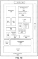
- a first communication chip 1006 may be dedicated to shorter range wireless communications such as Wi-Fi, WiGig, and Bluetooth and a second communication chip 1006 may be dedicated to longer range wireless communications such as GPS, EDGE, GPRS, CDMA, WiMAX, LTE, Ev-DO, 5G, and others.
Landscapes
- Engineering & Computer Science (AREA)
- Manufacturing & Machinery (AREA)
- Physics & Mathematics (AREA)
- Acoustics & Sound (AREA)
- Piezo-Electric Or Mechanical Vibrators, Or Delay Or Filter Circuits (AREA)
Abstract
Description
Claims (20)
Applications Claiming Priority (1)
| Application Number | Priority Date | Filing Date | Title |
|---|---|---|---|
| PCT/US2016/068352 WO2018118069A1 (en) | 2016-12-22 | 2016-12-22 | Microelectronic devices having vertical piezoelectric membranes for integrated rf filters |
Publications (2)
| Publication Number | Publication Date |
|---|---|
| US20190260342A1 US20190260342A1 (en) | 2019-08-22 |
| US11005447B2 true US11005447B2 (en) | 2021-05-11 |
Family
ID=62627055
Family Applications (1)
| Application Number | Title | Priority Date | Filing Date |
|---|---|---|---|
| US16/346,099 Active 2036-12-25 US11005447B2 (en) | 2016-12-22 | 2016-12-22 | Microelectronic devices having vertical piezoelectric membranes for integrated RF filters |
Country Status (2)
| Country | Link |
|---|---|
| US (1) | US11005447B2 (en) |
| WO (1) | WO2018118069A1 (en) |
Families Citing this family (3)
| Publication number | Priority date | Publication date | Assignee | Title |
|---|---|---|---|---|
| CN112448686B (en) * | 2019-09-05 | 2023-05-02 | 芯恩(青岛)集成电路有限公司 | Nanomaterial bulk acoustic wave resonator and preparation method thereof |
| CN113364423B (en) * | 2021-05-27 | 2023-11-10 | 广州乐仪投资有限公司 | Piezoelectric MEMS resonator, forming method thereof and electronic equipment |
| CN119210373A (en) * | 2024-09-13 | 2024-12-27 | 深圳新声半导体有限公司 | Method for manufacturing filter and filter |
Citations (6)
| Publication number | Priority date | Publication date | Assignee | Title |
|---|---|---|---|---|
| US20050030128A1 (en) | 2001-12-17 | 2005-02-10 | Intel Corporation | Film bulk acoustic resonator structure and method of making |
| US20060017523A1 (en) | 2004-06-04 | 2006-01-26 | The Regents Of The University Of California | Internal electrostatic transduction structures for bulk-mode micromechanical resonators |
| US20060044078A1 (en) | 2004-08-24 | 2006-03-02 | Farrokh Ayazi | Capacitive vertical silicon bulk acoustic resonator |
| US20100019869A1 (en) | 2008-07-11 | 2010-01-28 | Stmicroelectronics S.A. | Bulk mode resonator |
| US20140292155A1 (en) | 2011-10-05 | 2014-10-02 | Universite De Franche-Comte | Electro-acoustic transducer with periodic ferroelectric polarization produced on a micromachined vertical structure |
| US9013089B2 (en) * | 2013-01-02 | 2015-04-21 | Industrial Technology Research Institute | Microelectromechanical system-based resonator device |
-
2016
- 2016-12-22 WO PCT/US2016/068352 patent/WO2018118069A1/en not_active Ceased
- 2016-12-22 US US16/346,099 patent/US11005447B2/en active Active
Patent Citations (6)
| Publication number | Priority date | Publication date | Assignee | Title |
|---|---|---|---|---|
| US20050030128A1 (en) | 2001-12-17 | 2005-02-10 | Intel Corporation | Film bulk acoustic resonator structure and method of making |
| US20060017523A1 (en) | 2004-06-04 | 2006-01-26 | The Regents Of The University Of California | Internal electrostatic transduction structures for bulk-mode micromechanical resonators |
| US20060044078A1 (en) | 2004-08-24 | 2006-03-02 | Farrokh Ayazi | Capacitive vertical silicon bulk acoustic resonator |
| US20100019869A1 (en) | 2008-07-11 | 2010-01-28 | Stmicroelectronics S.A. | Bulk mode resonator |
| US20140292155A1 (en) | 2011-10-05 | 2014-10-02 | Universite De Franche-Comte | Electro-acoustic transducer with periodic ferroelectric polarization produced on a micromachined vertical structure |
| US9013089B2 (en) * | 2013-01-02 | 2015-04-21 | Industrial Technology Research Institute | Microelectromechanical system-based resonator device |
Non-Patent Citations (5)
| Title |
|---|
| "Piezoelectric MEMS Resonator", chapter 1 on AIN thin film Processing and Basic Properties by Paul Muralt, Piezoelectric MEMS Resonator, Springer, Switzerland, 2017 (Year: 2017). * |
| "Semiconductor and Optoelectronics", Prof. V. Krishnan, Department of Physics, Periyar University, Salem-636011 India (Year: 2019). * |
| International Preliminary Report on Patentability for International Patent Application No. PCT/US2016/068352 dated Jul. 4, 2019, 10 pgs. |
| International Search Report and Written Opinion for International Patent Application No. PCT/US2016/068352 dated Sep. 14, 2017, 13 pgs. |
| Tamariz et al. "AIN grown on Si(111) by ammonia-molecular beam epitaxy in the 900-1200° C. temperature range", published in the Journal of Crystal Growth, Aug. 2017 (Year: 2017). * |
Also Published As
| Publication number | Publication date |
|---|---|
| US20190260342A1 (en) | 2019-08-22 |
| WO2018118069A1 (en) | 2018-06-28 |
Similar Documents
| Publication | Publication Date | Title |
|---|---|---|
| TWI733881B (en) | Single-flipped resonator devices with 2deg bottom electrode | |
| US11616488B2 (en) | FBAR devices having multiple epitaxial layers stacked on a same substrate | |
| US10700665B2 (en) | Film bulk acoustic resonator (FBAR) devices for high frequency RF filters | |
| US10439057B2 (en) | Multi-gate high electron mobility transistors and methods of fabrication | |
| TWI517217B (en) | Nanostructure and Nanostructure of Si(111) Plane on Si(100) Wafer for III-N Epitaxial | |
| US11043627B2 (en) | Techniques for monolithic co-integration of thin-film bulk acoustic resonator devices and III-N semiconductor transistor devices | |
| KR20160111364A (en) | Iii-n devices in si trenches | |
| US10673405B2 (en) | Film bulk acoustic resonator (FBAR) devices with 2DEG bottom electrode | |
| US11218133B2 (en) | Film bulk acoustic resonator (FBAR) devices for high frequency RF filters | |
| US12148690B2 (en) | Microelectronic devices having air gap structures integrated with interconnect for reduced parasitic capacitances | |
| US11671075B2 (en) | Film bulk acoustic resonator (FBAR) devices for high frequency RF filters | |
| US11005447B2 (en) | Microelectronic devices having vertical piezoelectric membranes for integrated RF filters | |
| US11056532B2 (en) | Techniques for monolithic co-integration of polycrystalline thin-film bulk acoustic resonator devices and monocrystalline III-N semiconductor transistor devices | |
| TW201826702A (en) | Film bulk acoustic resonator (fbar) rf filter having epitaxial layers | |
| US10096474B2 (en) | Methods and structures to prevent sidewall defects during selective epitaxy | |
| US11705882B2 (en) | Acoustic resonator structure |
Legal Events
| Date | Code | Title | Description |
|---|---|---|---|
| FEPP | Fee payment procedure |
Free format text: ENTITY STATUS SET TO UNDISCOUNTED (ORIGINAL EVENT CODE: BIG.); ENTITY STATUS OF PATENT OWNER: LARGE ENTITY |
|
| STPP | Information on status: patent application and granting procedure in general |
Free format text: APPLICATION DISPATCHED FROM PREEXAM, NOT YET DOCKETED |
|
| STPP | Information on status: patent application and granting procedure in general |
Free format text: DOCKETED NEW CASE - READY FOR EXAMINATION |
|
| STPP | Information on status: patent application and granting procedure in general |
Free format text: NON FINAL ACTION MAILED |
|
| STPP | Information on status: patent application and granting procedure in general |
Free format text: NOTICE OF ALLOWANCE MAILED -- APPLICATION RECEIVED IN OFFICE OF PUBLICATIONS |
|
| AS | Assignment |
Owner name: INTEL CORPORATION, CALIFORNIA Free format text: ASSIGNMENT OF ASSIGNORS INTEREST;ASSIGNORS:FISCHER, PAUL B.;RADOSAVLJEVIC, MARKO;DASGUPTA, SANSAPTAK;AND OTHERS;SIGNING DATES FROM 20161209 TO 20161212;REEL/FRAME:055657/0826 |
|
| STPP | Information on status: patent application and granting procedure in general |
Free format text: PUBLICATIONS -- ISSUE FEE PAYMENT RECEIVED |
|
| STPP | Information on status: patent application and granting procedure in general |
Free format text: PUBLICATIONS -- ISSUE FEE PAYMENT VERIFIED |
|
| STCF | Information on status: patent grant |
Free format text: PATENTED CASE |
|
| MAFP | Maintenance fee payment |
Free format text: PAYMENT OF MAINTENANCE FEE, 4TH YEAR, LARGE ENTITY (ORIGINAL EVENT CODE: M1551); ENTITY STATUS OF PATENT OWNER: LARGE ENTITY Year of fee payment: 4 |