US11003003B2 - Display device - Google Patents
Display device Download PDFInfo
- Publication number
- US11003003B2 US11003003B2 US16/918,453 US202016918453A US11003003B2 US 11003003 B2 US11003003 B2 US 11003003B2 US 202016918453 A US202016918453 A US 202016918453A US 11003003 B2 US11003003 B2 US 11003003B2
- Authority
- US
- United States
- Prior art keywords
- display device
- area
- thin film
- film transistor
- insulating film
- Prior art date
- Legal status (The legal status is an assumption and is not a legal conclusion. Google has not performed a legal analysis and makes no representation as to the accuracy of the status listed.)
- Active
Links
Images


Classifications
-
- G—PHYSICS
- G02—OPTICS
- G02F—OPTICAL DEVICES OR ARRANGEMENTS FOR THE CONTROL OF LIGHT BY MODIFICATION OF THE OPTICAL PROPERTIES OF THE MEDIA OF THE ELEMENTS INVOLVED THEREIN; NON-LINEAR OPTICS; FREQUENCY-CHANGING OF LIGHT; OPTICAL LOGIC ELEMENTS; OPTICAL ANALOGUE/DIGITAL CONVERTERS
- G02F1/00—Devices or arrangements for the control of the intensity, colour, phase, polarisation or direction of light arriving from an independent light source, e.g. switching, gating or modulating; Non-linear optics
- G02F1/01—Devices or arrangements for the control of the intensity, colour, phase, polarisation or direction of light arriving from an independent light source, e.g. switching, gating or modulating; Non-linear optics for the control of the intensity, phase, polarisation or colour
- G02F1/13—Devices or arrangements for the control of the intensity, colour, phase, polarisation or direction of light arriving from an independent light source, e.g. switching, gating or modulating; Non-linear optics for the control of the intensity, phase, polarisation or colour based on liquid crystals, e.g. single liquid crystal display cells
- G02F1/133—Constructional arrangements; Operation of liquid crystal cells; Circuit arrangements
- G02F1/1333—Constructional arrangements; Manufacturing methods
- G02F1/1345—Conductors connecting electrodes to cell terminals
-
- G—PHYSICS
- G02—OPTICS
- G02F—OPTICAL DEVICES OR ARRANGEMENTS FOR THE CONTROL OF LIGHT BY MODIFICATION OF THE OPTICAL PROPERTIES OF THE MEDIA OF THE ELEMENTS INVOLVED THEREIN; NON-LINEAR OPTICS; FREQUENCY-CHANGING OF LIGHT; OPTICAL LOGIC ELEMENTS; OPTICAL ANALOGUE/DIGITAL CONVERTERS
- G02F1/00—Devices or arrangements for the control of the intensity, colour, phase, polarisation or direction of light arriving from an independent light source, e.g. switching, gating or modulating; Non-linear optics
- G02F1/01—Devices or arrangements for the control of the intensity, colour, phase, polarisation or direction of light arriving from an independent light source, e.g. switching, gating or modulating; Non-linear optics for the control of the intensity, phase, polarisation or colour
- G02F1/13—Devices or arrangements for the control of the intensity, colour, phase, polarisation or direction of light arriving from an independent light source, e.g. switching, gating or modulating; Non-linear optics for the control of the intensity, phase, polarisation or colour based on liquid crystals, e.g. single liquid crystal display cells
- G02F1/133—Constructional arrangements; Operation of liquid crystal cells; Circuit arrangements
- G02F1/1333—Constructional arrangements; Manufacturing methods
- G02F1/133305—Flexible substrates, e.g. plastics, organic film
-
- G—PHYSICS
- G02—OPTICS
- G02F—OPTICAL DEVICES OR ARRANGEMENTS FOR THE CONTROL OF LIGHT BY MODIFICATION OF THE OPTICAL PROPERTIES OF THE MEDIA OF THE ELEMENTS INVOLVED THEREIN; NON-LINEAR OPTICS; FREQUENCY-CHANGING OF LIGHT; OPTICAL LOGIC ELEMENTS; OPTICAL ANALOGUE/DIGITAL CONVERTERS
- G02F1/00—Devices or arrangements for the control of the intensity, colour, phase, polarisation or direction of light arriving from an independent light source, e.g. switching, gating or modulating; Non-linear optics
- G02F1/01—Devices or arrangements for the control of the intensity, colour, phase, polarisation or direction of light arriving from an independent light source, e.g. switching, gating or modulating; Non-linear optics for the control of the intensity, phase, polarisation or colour
- G02F1/13—Devices or arrangements for the control of the intensity, colour, phase, polarisation or direction of light arriving from an independent light source, e.g. switching, gating or modulating; Non-linear optics for the control of the intensity, phase, polarisation or colour based on liquid crystals, e.g. single liquid crystal display cells
- G02F1/133—Constructional arrangements; Operation of liquid crystal cells; Circuit arrangements
- G02F1/1333—Constructional arrangements; Manufacturing methods
- G02F1/1335—Structural association of cells with optical devices, e.g. polarisers or reflectors
- G02F1/133509—Filters, e.g. light shielding masks
- G02F1/133512—Light shielding layers, e.g. black matrix
-
- G—PHYSICS
- G02—OPTICS
- G02F—OPTICAL DEVICES OR ARRANGEMENTS FOR THE CONTROL OF LIGHT BY MODIFICATION OF THE OPTICAL PROPERTIES OF THE MEDIA OF THE ELEMENTS INVOLVED THEREIN; NON-LINEAR OPTICS; FREQUENCY-CHANGING OF LIGHT; OPTICAL LOGIC ELEMENTS; OPTICAL ANALOGUE/DIGITAL CONVERTERS
- G02F1/00—Devices or arrangements for the control of the intensity, colour, phase, polarisation or direction of light arriving from an independent light source, e.g. switching, gating or modulating; Non-linear optics
- G02F1/01—Devices or arrangements for the control of the intensity, colour, phase, polarisation or direction of light arriving from an independent light source, e.g. switching, gating or modulating; Non-linear optics for the control of the intensity, phase, polarisation or colour
- G02F1/13—Devices or arrangements for the control of the intensity, colour, phase, polarisation or direction of light arriving from an independent light source, e.g. switching, gating or modulating; Non-linear optics for the control of the intensity, phase, polarisation or colour based on liquid crystals, e.g. single liquid crystal display cells
- G02F1/133—Constructional arrangements; Operation of liquid crystal cells; Circuit arrangements
- G02F1/1333—Constructional arrangements; Manufacturing methods
- G02F1/1335—Structural association of cells with optical devices, e.g. polarisers or reflectors
- G02F1/133509—Filters, e.g. light shielding masks
- G02F1/133514—Colour filters
-
- G—PHYSICS
- G02—OPTICS
- G02F—OPTICAL DEVICES OR ARRANGEMENTS FOR THE CONTROL OF LIGHT BY MODIFICATION OF THE OPTICAL PROPERTIES OF THE MEDIA OF THE ELEMENTS INVOLVED THEREIN; NON-LINEAR OPTICS; FREQUENCY-CHANGING OF LIGHT; OPTICAL LOGIC ELEMENTS; OPTICAL ANALOGUE/DIGITAL CONVERTERS
- G02F1/00—Devices or arrangements for the control of the intensity, colour, phase, polarisation or direction of light arriving from an independent light source, e.g. switching, gating or modulating; Non-linear optics
- G02F1/01—Devices or arrangements for the control of the intensity, colour, phase, polarisation or direction of light arriving from an independent light source, e.g. switching, gating or modulating; Non-linear optics for the control of the intensity, phase, polarisation or colour
- G02F1/13—Devices or arrangements for the control of the intensity, colour, phase, polarisation or direction of light arriving from an independent light source, e.g. switching, gating or modulating; Non-linear optics for the control of the intensity, phase, polarisation or colour based on liquid crystals, e.g. single liquid crystal display cells
- G02F1/133—Constructional arrangements; Operation of liquid crystal cells; Circuit arrangements
- G02F1/1333—Constructional arrangements; Manufacturing methods
- G02F1/1339—Gaskets; Spacers; Sealing of cells
-
- G—PHYSICS
- G02—OPTICS
- G02F—OPTICAL DEVICES OR ARRANGEMENTS FOR THE CONTROL OF LIGHT BY MODIFICATION OF THE OPTICAL PROPERTIES OF THE MEDIA OF THE ELEMENTS INVOLVED THEREIN; NON-LINEAR OPTICS; FREQUENCY-CHANGING OF LIGHT; OPTICAL LOGIC ELEMENTS; OPTICAL ANALOGUE/DIGITAL CONVERTERS
- G02F1/00—Devices or arrangements for the control of the intensity, colour, phase, polarisation or direction of light arriving from an independent light source, e.g. switching, gating or modulating; Non-linear optics
- G02F1/01—Devices or arrangements for the control of the intensity, colour, phase, polarisation or direction of light arriving from an independent light source, e.g. switching, gating or modulating; Non-linear optics for the control of the intensity, phase, polarisation or colour
- G02F1/13—Devices or arrangements for the control of the intensity, colour, phase, polarisation or direction of light arriving from an independent light source, e.g. switching, gating or modulating; Non-linear optics for the control of the intensity, phase, polarisation or colour based on liquid crystals, e.g. single liquid crystal display cells
- G02F1/133—Constructional arrangements; Operation of liquid crystal cells; Circuit arrangements
- G02F1/136—Liquid crystal cells structurally associated with a semi-conducting layer or substrate, e.g. cells forming part of an integrated circuit
- G02F1/1362—Active matrix addressed cells
- G02F1/136286—Wiring, e.g. gate line, drain line
-
- G—PHYSICS
- G02—OPTICS
- G02F—OPTICAL DEVICES OR ARRANGEMENTS FOR THE CONTROL OF LIGHT BY MODIFICATION OF THE OPTICAL PROPERTIES OF THE MEDIA OF THE ELEMENTS INVOLVED THEREIN; NON-LINEAR OPTICS; FREQUENCY-CHANGING OF LIGHT; OPTICAL LOGIC ELEMENTS; OPTICAL ANALOGUE/DIGITAL CONVERTERS
- G02F1/00—Devices or arrangements for the control of the intensity, colour, phase, polarisation or direction of light arriving from an independent light source, e.g. switching, gating or modulating; Non-linear optics
- G02F1/01—Devices or arrangements for the control of the intensity, colour, phase, polarisation or direction of light arriving from an independent light source, e.g. switching, gating or modulating; Non-linear optics for the control of the intensity, phase, polarisation or colour
- G02F1/13—Devices or arrangements for the control of the intensity, colour, phase, polarisation or direction of light arriving from an independent light source, e.g. switching, gating or modulating; Non-linear optics for the control of the intensity, phase, polarisation or colour based on liquid crystals, e.g. single liquid crystal display cells
- G02F1/133—Constructional arrangements; Operation of liquid crystal cells; Circuit arrangements
- G02F1/136—Liquid crystal cells structurally associated with a semi-conducting layer or substrate, e.g. cells forming part of an integrated circuit
- G02F1/1362—Active matrix addressed cells
- G02F1/1368—Active matrix addressed cells in which the switching element is a three-electrode device
-
- G—PHYSICS
- G09—EDUCATION; CRYPTOGRAPHY; DISPLAY; ADVERTISING; SEALS
- G09F—DISPLAYING; ADVERTISING; SIGNS; LABELS OR NAME-PLATES; SEALS
- G09F9/00—Indicating arrangements for variable information in which the information is built-up on a support by selection or combination of individual elements
- G09F9/30—Indicating arrangements for variable information in which the information is built-up on a support by selection or combination of individual elements in which the desired character or characters are formed by combining individual elements
- G09F9/301—Indicating arrangements for variable information in which the information is built-up on a support by selection or combination of individual elements in which the desired character or characters are formed by combining individual elements flexible foldable or roll-able electronic displays, e.g. thin LCD, OLED
-
- H01L27/1214—
-
- H01L27/1218—
-
- H01L27/1244—
-
- H01L27/3276—
-
- H01L51/0097—
-
- H—ELECTRICITY
- H05—ELECTRIC TECHNIQUES NOT OTHERWISE PROVIDED FOR
- H05K—PRINTED CIRCUITS; CASINGS OR CONSTRUCTIONAL DETAILS OF ELECTRIC APPARATUS; MANUFACTURE OF ASSEMBLAGES OF ELECTRICAL COMPONENTS
- H05K1/00—Printed circuits
- H05K1/18—Printed circuits structurally associated with non-printed electric components
- H05K1/189—Printed circuits structurally associated with non-printed electric components characterised by the use of a flexible or folded printed circuit
-
- H—ELECTRICITY
- H10—SEMICONDUCTOR DEVICES; ELECTRIC SOLID-STATE DEVICES NOT OTHERWISE PROVIDED FOR
- H10D—INORGANIC ELECTRIC SEMICONDUCTOR DEVICES
- H10D86/00—Integrated devices formed in or on insulating or conducting substrates, e.g. formed in silicon-on-insulator [SOI] substrates or on stainless steel or glass substrates
- H10D86/40—Integrated devices formed in or on insulating or conducting substrates, e.g. formed in silicon-on-insulator [SOI] substrates or on stainless steel or glass substrates characterised by multiple TFTs
- H10D86/411—Integrated devices formed in or on insulating or conducting substrates, e.g. formed in silicon-on-insulator [SOI] substrates or on stainless steel or glass substrates characterised by multiple TFTs characterised by materials, geometry or structure of the substrates
-
- H—ELECTRICITY
- H10—SEMICONDUCTOR DEVICES; ELECTRIC SOLID-STATE DEVICES NOT OTHERWISE PROVIDED FOR
- H10D—INORGANIC ELECTRIC SEMICONDUCTOR DEVICES
- H10D86/00—Integrated devices formed in or on insulating or conducting substrates, e.g. formed in silicon-on-insulator [SOI] substrates or on stainless steel or glass substrates
- H10D86/40—Integrated devices formed in or on insulating or conducting substrates, e.g. formed in silicon-on-insulator [SOI] substrates or on stainless steel or glass substrates characterised by multiple TFTs
- H10D86/441—Interconnections, e.g. scanning lines
- H10D86/443—Interconnections, e.g. scanning lines adapted for preventing breakage, peeling or short circuiting
-
- H—ELECTRICITY
- H10—SEMICONDUCTOR DEVICES; ELECTRIC SOLID-STATE DEVICES NOT OTHERWISE PROVIDED FOR
- H10D—INORGANIC ELECTRIC SEMICONDUCTOR DEVICES
- H10D86/00—Integrated devices formed in or on insulating or conducting substrates, e.g. formed in silicon-on-insulator [SOI] substrates or on stainless steel or glass substrates
- H10D86/40—Integrated devices formed in or on insulating or conducting substrates, e.g. formed in silicon-on-insulator [SOI] substrates or on stainless steel or glass substrates characterised by multiple TFTs
- H10D86/60—Integrated devices formed in or on insulating or conducting substrates, e.g. formed in silicon-on-insulator [SOI] substrates or on stainless steel or glass substrates characterised by multiple TFTs wherein the TFTs are in active matrices
-
- H—ELECTRICITY
- H10—SEMICONDUCTOR DEVICES; ELECTRIC SOLID-STATE DEVICES NOT OTHERWISE PROVIDED FOR
- H10K—ORGANIC ELECTRIC SOLID-STATE DEVICES
- H10K59/00—Integrated devices, or assemblies of multiple devices, comprising at least one organic light-emitting element covered by group H10K50/00
- H10K59/10—OLED displays
- H10K59/12—Active-matrix OLED [AMOLED] displays
- H10K59/131—Interconnections, e.g. wiring lines or terminals
-
- H—ELECTRICITY
- H10—SEMICONDUCTOR DEVICES; ELECTRIC SOLID-STATE DEVICES NOT OTHERWISE PROVIDED FOR
- H10K—ORGANIC ELECTRIC SOLID-STATE DEVICES
- H10K77/00—Constructional details of devices covered by this subclass and not covered by groups H10K10/80, H10K30/80, H10K50/80 or H10K59/80
- H10K77/10—Substrates, e.g. flexible substrates
- H10K77/111—Flexible substrates
-
- H01L2251/5338—
-
- H—ELECTRICITY
- H05—ELECTRIC TECHNIQUES NOT OTHERWISE PROVIDED FOR
- H05K—PRINTED CIRCUITS; CASINGS OR CONSTRUCTIONAL DETAILS OF ELECTRIC APPARATUS; MANUFACTURE OF ASSEMBLAGES OF ELECTRICAL COMPONENTS
- H05K2201/00—Indexing scheme relating to printed circuits covered by H05K1/00
- H05K2201/05—Flexible printed circuits [FPCs]
-
- H—ELECTRICITY
- H10—SEMICONDUCTOR DEVICES; ELECTRIC SOLID-STATE DEVICES NOT OTHERWISE PROVIDED FOR
- H10K—ORGANIC ELECTRIC SOLID-STATE DEVICES
- H10K2102/00—Constructional details relating to the organic devices covered by this subclass
- H10K2102/301—Details of OLEDs
- H10K2102/311—Flexible OLED
-
- Y—GENERAL TAGGING OF NEW TECHNOLOGICAL DEVELOPMENTS; GENERAL TAGGING OF CROSS-SECTIONAL TECHNOLOGIES SPANNING OVER SEVERAL SECTIONS OF THE IPC; TECHNICAL SUBJECTS COVERED BY FORMER USPC CROSS-REFERENCE ART COLLECTIONS [XRACs] AND DIGESTS
- Y02—TECHNOLOGIES OR APPLICATIONS FOR MITIGATION OR ADAPTATION AGAINST CLIMATE CHANGE
- Y02E—REDUCTION OF GREENHOUSE GAS [GHG] EMISSIONS, RELATED TO ENERGY GENERATION, TRANSMISSION OR DISTRIBUTION
- Y02E10/00—Energy generation through renewable energy sources
- Y02E10/50—Photovoltaic [PV] energy
- Y02E10/549—Organic PV cells
Definitions
- the present invention relates to a display device specifically a flexible display device that a terminal area, which is outside of a display area, is bendable.
- the liquid crystal display device and the organic EL display device can be bendable by making the substrate thin.
- the substrate, on which display elements are formed is formed by thin glass or thin resin.
- the substrate is made of resin like polyimide, more flexible display devices can be realized.
- the patent document 1 Japanese patent application laid open No. 2014-197181 discloses bendable display devices, wherein the wirings are made thinner, or made thicker or bifurcated to prevent a breaking of the wirings at the bending portion.
- a bendable display device can be realized by forming the TFT (Thin Film Transistor) and etc. on the flexible substrate made of e.g. polyimide.
- the displays are comprised of many wiring layers and many insulating layers. The insulating layers are relatively hard; thus if they are bent in relatively small radius of curvature, they are broken. At the same time, the wirings that are formed on the insulating layer are also broken; consequently, the disconnections in the wirings occur.
- the purpose of the present invention is to avoid disconnection of the wirings due to breaking of the insulating layer at the bending portion in the bendable display device; thus, to realize a flexible display device of high reliability.
- the present invention overcomes the above explained problem; the concrete structures are as follows.
- a display device having a display area, a driving circuit area and a bending area comprising:
- a first thin film transistor and a first interlayer insulating film are formed in the display area
- a second thin film transistor and a second interlayer insulating film are formed in the driving circuit area
- the first thin film transistor, the second thin film transistor, the first interlayer insulating film and the second interlayer insulating film are removed in the bending area.
- a display device having a display area, a driving circuit area and a bending area comprising:
- a first thin film transistor and a first interlayer insulating film are formed in the display area
- a second thin film transistor and a second interlayer insulating film are formed in the driving circuit area
- the first thin film transistor, the second thin film transistor, the first interlayer insulating film and the second interlayer insulating film are removed to form a recess in the bending area
- terminal wirings extend in a first direction and are arranged in a second direction in the recess,
- the recess has a corner in a cross sectional view
- a first metal is formed in island shape under the terminal wiring at the corner of the recess,
- a width of the first metal in the second direction is bigger than a width of the terminal wiring in the second direction.
- FIG. 1 is a plan view of the liquid crystal display device according to the present invention.
- FIG. 2 is a plan view of another example of the liquid crystal display device according to the present invention.
- FIG. 3 is a plan view of yet another example of the liquid crystal display device according to the present invention.
- FIG. 4 is a plan view of further yet another example of the liquid crystal display device according to the present invention.
- FIG. 5 is cross sectional view along the line A-A in FIG. 1 as a comparative example of the liquid crystal display device
- FIG. 6 is a cross sectional view of the TFT substrate side of FIG. 5 ;
- FIG. 7 is a cross sectional view that shows a problem of the structure of FIG. 6 ;
- FIG. 8 is cross sectional view along the line A-A in FIG. 1 of the liquid crystal display device according to the present invention.
- FIG. 9 is a cross sectional view in an interim process to form the structure of FIG. 8 ;
- FIG. 10 is a cross sectional view in an interim process following FIG. 9 to form the structure of FIG. 8 ;
- FIG. 11 is a cross sectional view in an interim process following FIG. 10 to form the structure of FIG. 8 ;
- FIG. 12 is a cross sectional view in an interim process following FIG. 11 to form the structure of FIG. 8 ;
- FIG. 13 is a cross sectional view in an interim process following FIG. 12 to form the structure of FIG. 8 ;
- FIG. 14 is a cross sectional view of the embodiment 2;
- FIG. 15 is a cross sectional view of another example of the embodiment 2;
- FIG. 16A is a plan view of the embodiment 3;
- FIG. 16B is a cross sectional view along the B-B line of FIG. 16A ;
- FIG. 16C is a cross sectional view along the C-C line of FIG. 16A ;
- FIG. 17A is a plan view of the embodiment 3;
- FIG. 17B is a cross sectional view along the D-D line of FIG. 17A ;
- FIG. 17C is a cross sectional view along the E-E line of FIG. 17A ;
- FIG. 18A is a plan view of another example of the embodiment 3.
- FIG. 18B is a cross sectional view along the G-G line of FIG. 18A ;
- FIG. 18C is a cross sectional view along the H-H line of FIG. 18A ;
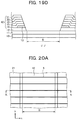
- FIG. 19A is a plan view of the embodiment 4.
- FIG. 19B is a perspective view of FIG. 19A ;
- FIG. 19C is a cross sectional view along the I-I line of FIG. 19A ;
- FIG. 19D is a cross sectional view along the J-J line of FIG. 19A ;
- FIG. 20A is a plan view of the bending area as a comparative example to the embodiment 5;
- FIG. 20B is a cross sectional view along the K-K line of FIG. 20A ;
- FIG. 21 is a plan view of the bending area according to the embodiment 5.
- FIG. 22 is a plan view of the bending area according to another example of the embodiment 5;
- the outer size of the display device can be made small while keeping good visibility of the display screen by keeping the display area flat while making bendable only the terminal area.
- a reliability of the display device can be improved by keeping the display area and the peripheral driving circuit area flat, where many Thin Film Transistors (herein after TFT) and so on are formed.
- FIGS. 1 through 4 are the examples that the driving circuit is disposed at the area that is not bent.
- FIG. 1 is a plan view of the flexible display device that the terminal area is to be bent.
- FIG. 1 is an example of the liquid crystal display device.
- the scanning lines 1 extend in the lateral direction and are arranged in the longitudinal direction;
- the video signal lines 2 extend in the longitudinal direction and are arrange in the lateral direction.
- common lines 3 extend in the lateral direction; however, in an actual device, the common electrode that the common voltage is applied is distributed all over the display area in a plane shaped.
- the area surrounded by the scanning lines 1 and the video signal lines 2 is the pixel 4 ; the switching TFT is formed in every one of pixels 4 .
- the TFT connects with the pixel electrode, the liquid crystal layer LCD exists between the pixel electrode and the common electrode, the storage capacitance CST is formed between the pixel electrode and the common electrode.
- the scanning line driving circuits Y-Dr are disposed at the both sides of the display area 50 .
- the video signal line driving circuit X-Dr is disposed in the terminal area; however, in FIG. 1 , the video signal line driving circuit X-Dr is disposed apart from the display area 50 to avoid the bending area B.
- the longitudinal width in FIG. 1 of the bending area B is e.g. 1 mm to 5 mm.
- the video signal line driving circuit X-Dr and the display area 50 are connected by the terminal wirings 5 .
- the flexible wiring substrate FPC is connected to the edge of the terminal area to supply the power and signals to the liquid crystal display device.
- FIG. 2 is the same structure as FIG. 1 except that the video signal line driving circuit X-Dr is installed on the flexible wiring substrate FPC.
- FIG. 3 is an example that the video signal line driving circuit X-Dr is disposed adjacent to the display area 50 and the bending area B is formed between the video signal line driving circuit X-Dr and the flexible wiring substrate FPC.
- FIG. 4 is an example that the terminal areas are formed at the two sides of the display area 50 . In FIG. 4 , the bending areas B are formed to avoid the areas that the scanning line driving circuit Y-Dr and the video signal line driving circuit X-Dr are disposed in the terminal areas.
- FIG. 5 is cross sectional view of the liquid crystal display device corresponding to FIG. 1 along the line A-A.
- left hand side is the display area; the right hand side is the driving circuit.
- the area B between the display area and the driving circuit is the area to be bent.
- the liquid crystal display device explained below is for the In Plane Switching (IPS) type liquid crystal display device; however, the present invention is applicable to other types of liquid crystal display devices.
- IPS In Plane Switching
- the TFTs having the oxide semiconductors 16 are formed in the display area.
- the leak current can be made small in the TFT of the oxide semiconductor layer 16 .
- the oxide semiconductors that are optically transparent and amorphous are called TAOS (Transparent Amorphous Oxide Semiconductor).
- the examples of TAOS are IGZO (Indium Gallium Zinc Oxide), ITZO (Indium Tin Zinc Oxide), ZnON (Zinc Oxide Nitride), IGO (Indium Gallium Oxide), and so on.
- IGZO Indium Gallium Zinc Oxide
- ITZO Indium Tin Zinc Oxide
- ZnON Zinc Oxide Nitride
- IGO Indium Gallium Oxide
- IGZO is used for the oxide semiconductor layer 16 .
- the similar TFTs are used in the driving circuits, too.
- the TFT substrate 11 made of resin is formed on the glass substrate 10 .
- the polyimide is the most favorable among the resins for the TFT substrate 11 considering mechanical strength and heat resistance and so on.
- the glass substrate 10 is necessary in the manufacturing process; the glass substrate 10 is removed by e.g. laser abrasion from the TFT substrate 11 made of polyimide after the display device is completed.
- the barrier film 12 is formed on the TFT substrate 11 to prevent the semiconductor layer 16 from being contaminated by impurities from the TFT substrate 11 of polyimide.
- the barrier film 12 is formed by e.g. a laminated film of the silicon oxide (herein after SiO) film and the silicon nitride (herein after SiN) film.
- the light shield metal 13 made of metal is formed on the barrier film 12 .
- the light shield metal 13 has a role to shield the light from the back light to prevent the photo current in the semiconductor layer 16 .
- the first undercoat film 14 made of SiN is formed covering the light shield metal 13 ;
- the second undercoat film 15 made of SiO is formed on the first undercoat film 14 .
- the oxide semiconductor layer 16 made of IGZO is formed on the second undercoat film 15 .
- the gate insulating film 17 made of SiO is formed on the oxide semiconductor layer 16 ; the gate electrode 18 is formed on the gate insulating film 17 .
- the gate electrode 18 is made either one of MoW, Al, or Ti, etc. After the gate electrode 18 is formed, the drain region and the source region are formed in the semiconductor layer 16 either by: the ion implantation of e.g. Ar using the gate electrode 18 as the mask, or deoxidization by hydrogen using the gate electrode 18 as the mask.
- the first interlayer insulating film 19 made of SiO is formed to cover the gate electrode 18 ; the second interlayer insulating film 20 made of SiN is formed on the first interlayer insulating film 19 ; the third interlayer insulating film 21 made of SiO is formed on the second interlayer insulating film 20 .
- the through hole 30 is made through the first interlayer insulating film 19 to the third interlayer insulating film 21 to connect the source region and the source electrode 22 ; and the through hole 31 is made through the first interlayer insulating film 19 to the third interlayer insulating film 21 to connect the drain region and the drain electrode 23
- the organic passivation film 24 is formed covering the source electrode 22 and the drain electrode 23 . Since the organic passivation film 24 has a role of a flattening film, too, it is made as thick as 2-4 microns.
- the organic passivation film 24 is patterned to be removed from the terminal area, and at the same time, to form the through hole 32 in the organic passivation film 24 to connect the source electrode 22 and the pixel electrode 27 .
- the common electrode 25 is formed in a plane shape on the organic passivation film 24 ; the capacitive insulating film 26 made of SiN is formed on the common electrode 25 .
- the pixel electrode 27 is formed on the capacitive insulating film 26 .
- a plan view of the pixel electrode 27 is stripe shaped or comb shaped. When the area of the pixel is small, the pixel electrode tends to be a stripe shaped; when the area of the pixel is large, the pixel electrode 27 tends to be a comb shaped having a slit inside.
- the pixel capacitance is formed between the pixel electrode 27 and the common electrode 25 by sandwiching the capacitive insulating film 26 .
- the pixel electrode 27 connects with the source electrode 22 via the through hole 32 formed through the organic passivation film 24 and the capacitive insulating film 26 .
- the alignment film 28 which is for an initial alignment of the liquid crystal molecules 301 , is formed covering the pixel electrode 27 . Either rubbing method or photo alignment method that uses polarized ultra violet ray is applied to the alignment treatment of the alignment film 28 .
- the photo alignment method is advantageous in the IPS type liquid crystal display device.
- the line of force denoted by the arrow in FIG. 5 is generated when a video signal is applied to the pixel electrode 27 to rotate the liquid crystal molecules 301 ; thus, the transmittance of the liquid crystal layer 300 is controlled.
- the counter substrate 200 is disposed opposing to the TFT substrate 11 sandwiching the liquid crystal layer 300 .
- the counter substrate 200 and the TFT substrate 11 are adhered to each other by the sealing material 150 .
- the liquid crystal layer 300 is sealed inside from the sealing material 150 .
- the counter substrate 200 is made of glass; however, in the flexible display device, the counter substrate 200 is made of resin as e.g. polyimide.
- the color filter 201 and the black matrix 202 are formed on inside surface of the counter substrate 200 .
- the overcoat film 203 is formed covering the color filter 201 and the black matrix 202 .
- the alignment film 204 is formed covering the overcoat film 203 .
- the alignment treatment for the alignment film 204 is the same as explained for the alignment film 28 on the TFT substrate 11 .
- the driving circuit is formed at the right hand side of the bending area B.
- the driving circuit and the display area 50 are connected by the terminal wirings 5 .
- Many TFTs are formed in the driving circuit, too; however, the structure of the TFT is the same as the TFTs explained in regard to the display area 50 .
- the source of the TFT formed in the driving circuit connects with the circuit wiring 6 extended from the terminal wiring 5 via the through hole 33 .
- the drain of the TFT formed in the driving circuit connects with the circuit wiring 7 via the through hole 34 .
- FIG. 6 is a cross sectional view of the region from the display area to the bending area of the TFT substrate side in FIG. 5 .
- the terminal wiring 5 that connects the display area and the driving circuit is formed on the insulating layer formed by inorganic insulating films as the SiO film, the SiN film and the like.
- the inorganic insulating film is harder compared with the metal film, it is easily broken if it is bent. Then, it arises a phenomenon that the disconnection of the wiring occurs simultaneously when the insulating film is broken.
- FIG. 7 is a cross sectional view that shows this phenomenon.
- FIG. 7 is a cross sectional view that the polyimide substrate 11 is bent; wherein the inorganic insulating film 40 is formed on the polyimide substrate 11 ; the metal wiring 5 is formed on the inorganic insulating film 40 .
- the polyimide substrate 11 can be flexibly bent.
- the inorganic insulating film 40 is hard, thus, it is broken when it is bent.
- the inorganic insulating film 40 is a multi-layered film, the thickness tends to be big as a whole; consequently, stress becomes big if it is bent; thus, the inorganic insulating film 40 becomes easier to be broken.
- Even the metal wiring 5 is relatively flexible, when the insulating film 40 underneath is broken, the metal wiring 5 is also broken simultaneously, as depicted in FIG. 7 .
- FIG. 8 is a cross sectional view of the present invention that countermeasures the above explained problem.
- the structure of FIG. 8 is approximately the same as the structure explained in FIG. 5 except the bending area B.
- five inorganic insulating layers are eliminated; namely, the first undercoat film 14 , the second undercoat film 15 , the first interlayer insulating film 19 , the second interlayer insulating film 20 and the third interlayer insulating film 21 are removed.
- the display area and the driving circuit area are electrically connected by the terminal wirings 5 , which are formed by the same metal that constitutes the light shield metal 13 .
- the metal that constitutes the light shield metal 13 and the terminal wiring 5 is the same metal as the gate electrode as e.g. MoW. If the low electric resistance is required, the terminal wiring 5 is made as the structure that the layer of the aluminum as the major substance is sandwiched by the metal film of Ti or the metal film of Mo and the like.
- the TFT substrate 11 made of polyimide is formed on the glass substrate 10 ; the barrier film 12 is formed on the TFT substrate 11 ; the terminal wiring 5 is formed on the barrier film 12 .
- the glass substrate 10 is removed in the final structure of the display device. Therefore, the layers to be bent in the bending area B actually consist of the polyimide substrate 11 , the barrier film 12 and the terminal wirings 5 .
- the barrier film 12 is e.g. a two layer structure comprised of the SiO film and the SiN film. In the bending area B, however, five layers of first undercoat film 14 through the third interlayer insulating film 21 are removed, thus, the insulating layer as a whole is made thin. Therefore, the stress in the insulating film becomes less when it is bent, thus, the barrier film 12 is not broken. Consequently, the disconnection of the terminal wiring 5 , which is formed on the barrier film 12 , does not occur.
- the drain electrode 23 connects with the video signal line 2 ; the video signal line 2 connects with the terminal wiring 5 via the through hole 35 .
- the terminal wiring 5 connects with the circuit wiring 6 via the through hole 36 .
- Other structures in FIG. 8 are the same as explained in FIG. 5 .
- FIGS. 9 through 12 are cross sectional views of the TFT substrate side in the interim processes to realize the structure of FIG. 8 .
- the processes up to forming the barrier film 12 are the same as explained in FIG. 5 .
- the terminal wiring 5 is formed on the barrier film 12 simultaneously with the light shield metal 13 .
- the terminal wiring 5 is made of the same material as the light shield metal 13 and is made simultaneously as the light shield metal 13 .
- the subsequent processes up to the third interlayer insulating film 21 are the same as explained in FIG. 5 .
- the through holes are formed; in FIG. 9 , however, in addition to through holes formed in FIG. 5 , the recess 100 is formed in the bending area B by removing the first undercoat film 14 , the second undercoat film 15 , the first interlayer insulating film 19 , the second interlayer insulating film 20 , and the third interlayer insulating film 21 .
- the recess 100 can be made after the pixel electrode 27 is formed.
- the through hole 35 is formed in the display area, and the through hole 36 is formed in the driving circuit area in the undercoat films 14 , 15 and the interlayer insulating films 19 , 20 , 21 .
- the connections of the terminal wirings 5 with other wirings can be made.
- FIG. 10 shows that the source electrode 22 is formed in the through hole 30 , the drain electrode 23 is formed in the through hole 31 , the video signal line is formed in the through hole 35 , the circuit wiring 6 is formed in the through holes 33 , 36 , and the circuit wiring 7 is formed in the through hole 34 .
- the wirings in the display area, the wirings in the driving circuit, and the connection between the display area and the driving circuit are made.
- FIG. 11 is a cross sectional view that the organic passivation film 24 is formed covering the display area, the recess 100 and the driving circuit.
- the organic passivation film 24 is made of photo sensitive resin as acrylic. Since the organic passivation film 24 has a role as a flattening film in the display area, it is formed thick as 2 to 4 microns.
- FIG. 12 is a cross sectional view that the organic passivation film 24 is patterned. Since the organic passivation film 24 is made of the photo sensitive resin, it can be patterned without using the photo resist. After that, the organic passivation film 24 is put in calcination.
- FIG. 13 is a cross sectional view that the common electrode 25 , the capacitive insulating film 26 and the pixel electrode 27 are formed on the organic passivation film 24 , wherein the pixel electrode 27 and the source electrode 22 are connected via the through hole 32 in the display area. This structure is the same as explained in FIG. 5 .
- the counter substrate 200 is disposed and the liquid crystal is sealed inside; thus, the structure of FIG. 8 is completed.
- the breaking of the inorganic insulating film and a consequent disconnection of the wiring in the bending area B can be avoided by removing the plural layers of the inorganic insulating films from the bending area B; thus, flexible display device of high reliability can be realized.
- FIG. 14 is a cross sectional view of the TFT substrate side according to the embodiment 2.
- FIG. 14 differs from FIG. 10 of the embodiment 1 in that: the terminal wiring 5 that connects the display area and the driving circuit area is formed by the same wiring as the drain electrode 23 or the video signal line 2 .
- the drain electrode 23 and the terminal wiring 5 which is formed on the same layer as the light shield metal 13 , are connected via the through hole 35 ; and the circuit wiring 6 and the terminal wiring 5 are connected via the through hole 36 .
- the through holes 35 and 36 can be eliminated, thus, a reliability of connection can be improved.
- the light shield metal 13 is formed at the corner of the recess 100 in FIG. 14 . This is to avoid the resist remaining at the corner of the recess 100 as will be explained in the embodiment 3; however, the light shield metal 13 at the corner of the recess 100 is not indispensable.
- FIG. 15 is another example of the embodiment 3.
- FIG. 15 differs from FIG. 14 in that the terminal wiring is formed by two layers of a first layer 13 formed on the same layer as the light shield metal 13 and a second layer 5 that extends from the drain electrode 23 or the video signal line 2 . According to this structure, the danger of the disconnection of the terminal wiring 5 can be further diminished.
- FIG. 16A through 16C are figures to explain the problem in the recess 100 formed in the bending area B.
- FIG. 16A is a plan view of the bending area B.
- the terminal wirings 5 extend in the x direction across the recess 100 formed in the bending area B and are arranged in the y direction in a certain pitch.
- FIG. 16B is a cross sectional view along the line B-B in FIG. 16A .
- the resist remaining 101 exists at the corner of the recess 100 .
- the recess 100 is a deep hole through the five inorganic layers; consequently, the light for the exposure is difficult to reach at the corner of the deep hole, thus, there arises a chance that the resist at the corner of the recess is not thoroughly exposed to the light.
- FIG. 16C is a cross sectional view along the line C-C in FIG. 16A .
- the terminal wiring 5 made of metal exists at this portion. If the metal film exists at the corner of the recess 100 , the light is reflected by the metal film during the exposure, the reflected light can compensate the exposing light; thus, the resist remaining tends not to occur.
- FIGS. 17A through 17C are the example of the structure to decrease the chance of the resist remaining 101 .
- FIG. 17A is a plan view at the bending area B.
- the terminal wirings 5 extend in the x direction across the recess 100 and are arranged in the y direction in a certain pitch.
- the light shield metal 13 is formed in island shape under the terminal wiring at the corner of the recess 100 .
- FIG. 17B is a cross sectional view along the line D-D in FIG. 17A , namely, a cross sectional view along the line that crosses the light shield metal 13 formed in island shape in the x direction.
- the light shield metal 13 exists at the corner of the recess 100 , as indicated by the arrow; since the light reflected from the light shield metal 13 compensates the exposing light, the resist remaining does not occur.
- FIG. 17C is a cross sectional view along the line E-E in FIG. 17A .
- the light shield metal 13 and the terminal wiring 5 of two layer structure exist at the corner of the recess 100 , as indicated by the arrow; since the light reflected from the terminal wiring 5 compensates the exposing light, the resist remaining does not occur.
- FIGS. 18A through 18C are yet another example of the present embodiment.
- FIG. 18A is a plan view of the bending area B.
- the terminal wirings 5 extend in the x direction across the recess 100 formed in the bending area B and are arranged in the y direction with a certain pitch.
- the reflection metal 60 extends in the y direction with a width of w under the terminal wiring 5 via the barrier film 12 . The reflection metal 60 prevents the resist remaining at the corner of the recess 100 .
- FIG. 18B is a cross sectional view along the line G-G in FIG. 18A .
- the reflection metal 60 exists at the corner of the recess 100 as indicated by the arrow.
- the reflected light form the reflection metal 60 compensates the exposing light, thus, the resist remaining 101 does not occur.
- FIG. 18C is a cross sectional view along the line H-H in FIG. 18A .
- the terminal wiring 5 made of metal exists at the corner of the recess 100 as indicated by the arrow.
- the reflected light form the terminal wiring 5 compensates the exposing light, thus, the resist remaining 101 does not occur.
- the structure explained by 18 A through FIG. 18C , enables to utilize the reflection light at all the position of the corner of the recess 100 in the exposure, thus, the chance of the resist remaining can be substantially decreased.
- the structure, explained by 18 A through FIG. 18C needs to form the reflection metal 60 before the barrier film 12 is formed, thus, the process is increased. If an adhering strength between the reflection metal 60 and the polyimide substrate 11 is a problem, it is necessary to form the SiO film and the like between the reflection metal 60 and the polyimide substrate 11 to improve the adherence between the reflection metal 60 and the polyimide substrate 11 . In the meantime, if it is desired to remove the SiO film from the bending area B, a patterning of the SiO film is necessary. The patterning of the SiC film can be executed by the same photo lithography for the patterning of the reflection metal 60 .
- FIGS. 19A through 19D are figures to explain the embodiment 4.
- FIG. 19A is a plan view of the bending area B in embodiment 4.
- the terminal wirings 5 extend in the x direction across the recess 100 formed in the bending area B and are arranged in the y direction with a certain pitch.
- the polyimide substrate 11 is exposed to the surface in the recess 100 while the surface is the third interlayer insulating film 21 at places other than the recess 100 .
- FIG. 19B is a perspective view of FIG. 19A when it is viewed from the arrow in FIG. 19A .
- the light shield metal 13 and the barrier film 12 exist under the terminal wiring 5 ; however, in the area other than the portion of the terminal wiring 5 , the light shield metal 13 and the barrier film 12 are removed, thus, the polyimide substrate 11 is exposed. Namely, only one layer of the polyimide substrate 11 exists in the bending area B at the area other than the terminal wirings 5 are formed. By the way, the glass substrate 10 that is the lower most layer in FIG. 19B is removed at the last process.
- FIG. 19C is a cross sectional view along the line I-I in FIG. 19A
- FIG. 19D is a cross sectional view along the line J-J in FIG. 19A .
- the stress to the barrier film 12 is further reduced in this embodiment than in the structures of the embodiment 1 to the embodiment 3; thus, a danger of breaking of the barrier film 12 can be avoided. Consequently, the danger of disconnection of the terminal wiring 5 is further reduced.
- FIG. 20A through FIG. 22 are figures to explain the embodiment 5.
- FIG. 20A is a plan view of the bending area B explained in the embodiments 1 through 3.
- the terminal wirings 5 extend in the x direction in line, and arranged in the y direction in a predetermined pitch.
- FIG. 20B is a cross sectional view along the K-K line in FIG. 20A .
- the terminal wiring 5 extends along the inner wall and the bottom of the recess 100 in the bending area B.
- FIG. 21 is a plan view of the bending area B according to the present embodiment.
- the terminal wirings 5 extend in the x direction in zigzag shape and arranged in the y direction in a predetermined pitch.
- the cross sectional view of the bending area B in FIG. 21 is equivalent to FIG. 20B .
- the stress to the terminal wiring 5 can be less when it is in a zigzag shape than when it is in a straight line.
- the stress in the wiring 5 itself, can be reduced by making the terminal wiring 5 as the structure of FIG. 21 , the danger of disconnection of the terminal wiring 5 in the bending area can be further reduced.
- FIG. 22 is a plan view of the bending area B according to another example of the present embodiment.
- the terminal wirings extend in the x direction in wave shape and arranged in the y direction in a predetermined pitch.
- the cross sectional view of the bending area B in FIG. 22 is equivalent to FIG. 20B .
- the stress to the terminal wiring 5 can be less when it is in a wave shape than when it is in a straight line.
- the stress in the wiring 5 itself, can be reduced by making the terminal wiring 5 as the structure of FIG. 22 , the danger of disconnection of the terminal wiring 5 in the bending area can be further reduced.
- the light shield metal 13 is formed under the oxide semiconductor layer 16 ; the TFT can be made a dual gate type when the light shield metal 13 is used as the second gate electrode.
- both of the first undercoat film 14 and the second undercoat film 15 work as the gate insulating film.
- the second gate electrode can work as the light shield metal to shield the semiconductor layer 16 that constitutes the TFT from the back light.
- the semiconductor layer that constitutes the TFT is made of the oxide semiconductor; however, the semiconductor layer can be made of the poly-Si (poly-silicon) or a-Si (amorphous silicon).
- the liquid crystal display device is IPS type; however, the present invention is applicable to other types of the liquid crystal display devices.
- the present invention is applicable to the organic EL display device.
- the display area and the driving circuit are formed on the same substrate; and the bending area can be formed in the terminal area.
- the cross sectional structure of the organic EL display device is the same as the liquid crystal display device from the TFT substrate up to the organic passivation film, thus, the present invention explained above can be applicable to the organic EL display device.
Landscapes
- Physics & Mathematics (AREA)
- Nonlinear Science (AREA)
- General Physics & Mathematics (AREA)
- Mathematical Physics (AREA)
- Chemical & Material Sciences (AREA)
- Crystallography & Structural Chemistry (AREA)
- Optics & Photonics (AREA)
- Engineering & Computer Science (AREA)
- Microelectronics & Electronic Packaging (AREA)
- Theoretical Computer Science (AREA)
- Liquid Crystal (AREA)
- Devices For Indicating Variable Information By Combining Individual Elements (AREA)
Abstract
Description
Claims (20)
Priority Applications (1)
| Application Number | Priority Date | Filing Date | Title |
|---|---|---|---|
| US16/918,453 US11003003B2 (en) | 2017-10-26 | 2020-07-01 | Display device |
Applications Claiming Priority (5)
| Application Number | Priority Date | Filing Date | Title |
|---|---|---|---|
| JP2017-207020 | 2017-10-26 | ||
| JPJP2017-207020 | 2017-10-26 | ||
| JP2017207020A JP2019078927A (en) | 2017-10-26 | 2017-10-26 | Display |
| US16/153,861 US10761354B2 (en) | 2017-10-26 | 2018-10-08 | Display device |
| US16/918,453 US11003003B2 (en) | 2017-10-26 | 2020-07-01 | Display device |
Related Parent Applications (1)
| Application Number | Title | Priority Date | Filing Date |
|---|---|---|---|
| US16/153,861 Division US10761354B2 (en) | 2017-10-26 | 2018-10-08 | Display device |
Publications (2)
| Publication Number | Publication Date |
|---|---|
| US20200333652A1 US20200333652A1 (en) | 2020-10-22 |
| US11003003B2 true US11003003B2 (en) | 2021-05-11 |
Family
ID=66244876
Family Applications (2)
| Application Number | Title | Priority Date | Filing Date |
|---|---|---|---|
| US16/153,861 Active US10761354B2 (en) | 2017-10-26 | 2018-10-08 | Display device |
| US16/918,453 Active US11003003B2 (en) | 2017-10-26 | 2020-07-01 | Display device |
Family Applications Before (1)
| Application Number | Title | Priority Date | Filing Date |
|---|---|---|---|
| US16/153,861 Active US10761354B2 (en) | 2017-10-26 | 2018-10-08 | Display device |
Country Status (2)
| Country | Link |
|---|---|
| US (2) | US10761354B2 (en) |
| JP (1) | JP2019078927A (en) |
Families Citing this family (11)
| Publication number | Priority date | Publication date | Assignee | Title |
|---|---|---|---|---|
| KR102711136B1 (en) * | 2019-01-21 | 2024-09-27 | 삼성디스플레이 주식회사 | Dispcay device |
| KR102751443B1 (en) | 2019-03-25 | 2025-01-13 | 삼성디스플레이 주식회사 | Thin film transistor substrate, display apparatus and method of manufacturing the same |
| US12069915B2 (en) * | 2019-03-29 | 2024-08-20 | Sharp Kabushiki Kaisha | Display device and method for manufacturing same |
| US11244994B2 (en) * | 2019-10-23 | 2022-02-08 | Wuhan China Star Optoelectronics Semiconductor Display Technology Co., Ltd. | Thin film transistor array substrate and organic light emitting diode panel |
| CN110910755B (en) * | 2019-11-11 | 2021-09-03 | 武汉华星光电技术有限公司 | Display panel mother board and display panel |
| CN110930881B (en) * | 2019-11-28 | 2021-10-08 | 武汉华星光电半导体显示技术有限公司 | A flexible display module and flexible display device |
| CN111048566B (en) * | 2019-12-20 | 2022-04-01 | 厦门天马微电子有限公司 | Organic light-emitting display panel and display device |
| KR20220045602A (en) * | 2020-10-05 | 2022-04-13 | 삼성디스플레이 주식회사 | Display apparatus |
| CN113539099A (en) * | 2021-07-19 | 2021-10-22 | 京东方科技集团股份有限公司 | Display substrate and display device |
| WO2024245360A1 (en) * | 2023-05-30 | 2024-12-05 | 京东方科技集团股份有限公司 | Display substrate and display device |
| WO2025254336A1 (en) * | 2024-06-03 | 2025-12-11 | 삼성전자주식회사 | Electronic device and display device including transistor |
Citations (4)
| Publication number | Priority date | Publication date | Assignee | Title |
|---|---|---|---|---|
| US20110007042A1 (en) * | 2009-07-07 | 2011-01-13 | Semiconductor Energy Laboratory Co., Ltd. | Display device |
| US20140254111A1 (en) | 2013-03-07 | 2014-09-11 | Semiconductor Energy Laboratory Co., Ltd. | Display device |
| US20180173277A1 (en) * | 2016-12-16 | 2018-06-21 | Lg Display Co., Ltd. | Flexible display device |
| US20200027958A1 (en) | 2017-03-30 | 2020-01-23 | Sharp Kabushiki Kaisha | Active matrix substrate and liquid crystal display panel |
-
2017
- 2017-10-26 JP JP2017207020A patent/JP2019078927A/en active Pending
-
2018
- 2018-10-08 US US16/153,861 patent/US10761354B2/en active Active
-
2020
- 2020-07-01 US US16/918,453 patent/US11003003B2/en active Active
Patent Citations (5)
| Publication number | Priority date | Publication date | Assignee | Title |
|---|---|---|---|---|
| US20110007042A1 (en) * | 2009-07-07 | 2011-01-13 | Semiconductor Energy Laboratory Co., Ltd. | Display device |
| US20140254111A1 (en) | 2013-03-07 | 2014-09-11 | Semiconductor Energy Laboratory Co., Ltd. | Display device |
| JP2014197181A (en) | 2013-03-07 | 2014-10-16 | 株式会社半導体エネルギー研究所 | Display device |
| US20180173277A1 (en) * | 2016-12-16 | 2018-06-21 | Lg Display Co., Ltd. | Flexible display device |
| US20200027958A1 (en) | 2017-03-30 | 2020-01-23 | Sharp Kabushiki Kaisha | Active matrix substrate and liquid crystal display panel |
Also Published As
| Publication number | Publication date |
|---|---|
| US20190129227A1 (en) | 2019-05-02 |
| JP2019078927A (en) | 2019-05-23 |
| US10761354B2 (en) | 2020-09-01 |
| US20200333652A1 (en) | 2020-10-22 |
Similar Documents
| Publication | Publication Date | Title |
|---|---|---|
| US11003003B2 (en) | Display device | |
| JP5100968B2 (en) | Thin film transistor display panel and liquid crystal display device including the same | |
| US10761364B2 (en) | Liquid crystal display device | |
| US9524992B2 (en) | Thin film transistor array panel and manufacturing method thereof | |
| TWI578074B (en) | Thin film transistor substrate and display device | |
| US11906862B2 (en) | Display device and semiconductor device | |
| US7221424B2 (en) | Liquid crystal display having a horizontal electric field and capsulated pads and method of fabricating the same | |
| US20250159993A1 (en) | Display device and manufacturing method thereof | |
| US11774811B2 (en) | Display device having through holes without overhang in cross section | |
| US7023501B2 (en) | Liquid crystal display device having particular connections among drain and pixel electrodes and contact hole | |
| US10707240B2 (en) | Display device | |
| KR101272488B1 (en) | Thin Transistor Substrate, Method Of Fabricating The Same, Liquid Crystal Display Having The Same And Method Of Fabricating Liquid Crystal Display Having The Same | |
| KR101046923B1 (en) | Thin film transistor array panel and liquid crystal display including the same | |
| JP5090133B2 (en) | Liquid crystal display | |
| US9075273B2 (en) | Thin film transistor array panel and manufacturing method thereof | |
| KR100303440B1 (en) | Liquid crystal display of in-plane switching mode | |
| JP2009151285A (en) | Liquid crystal display device and method for manufacturing the same | |
| KR101754917B1 (en) | Thin film transistor array panel and manufacturing method thereof | |
| JP5055511B2 (en) | Horizontal electric field type liquid crystal display device | |
| KR20070120234A (en) | Color filter substrate, Display panel having same, and manufacturing method thereof | |
| JP2002108245A (en) | Matrix array substrate | |
| KR20240004011A (en) | Contact structure and display device using thereof | |
| KR100641000B1 (en) | LCD and its manufacturing method | |
| KR20040084597A (en) | Liquid crystal display apparatus of horizontal electronic field applying type and fabricating method thereof | |
| JP2006323186A (en) | Liquid crystal display device |
Legal Events
| Date | Code | Title | Description |
|---|---|---|---|
| FEPP | Fee payment procedure |
Free format text: ENTITY STATUS SET TO UNDISCOUNTED (ORIGINAL EVENT CODE: BIG.); ENTITY STATUS OF PATENT OWNER: LARGE ENTITY |
|
| STPP | Information on status: patent application and granting procedure in general |
Free format text: NOTICE OF ALLOWANCE MAILED -- APPLICATION RECEIVED IN OFFICE OF PUBLICATIONS |
|
| STPP | Information on status: patent application and granting procedure in general |
Free format text: PUBLICATIONS -- ISSUE FEE PAYMENT RECEIVED |
|
| STPP | Information on status: patent application and granting procedure in general |
Free format text: PUBLICATIONS -- ISSUE FEE PAYMENT VERIFIED Free format text: AWAITING TC RESP, ISSUE FEE PAYMENT VERIFIED |
|
| STPP | Information on status: patent application and granting procedure in general |
Free format text: PUBLICATIONS -- ISSUE FEE PAYMENT VERIFIED |
|
| STCF | Information on status: patent grant |
Free format text: PATENTED CASE |
|
| MAFP | Maintenance fee payment |
Free format text: PAYMENT OF MAINTENANCE FEE, 4TH YEAR, LARGE ENTITY (ORIGINAL EVENT CODE: M1551); ENTITY STATUS OF PATENT OWNER: LARGE ENTITY Year of fee payment: 4 |
|
| AS | Assignment |
Owner name: MAGNOLIA WHITE CORPORATION, JAPAN Free format text: ASSIGNMENT OF ASSIGNORS INTEREST;ASSIGNOR:JAPAN DISPLAY INC.;REEL/FRAME:072130/0313 Effective date: 20250625 Owner name: MAGNOLIA WHITE CORPORATION, JAPAN Free format text: ASSIGNMENT OF ASSIGNOR'S INTEREST;ASSIGNOR:JAPAN DISPLAY INC.;REEL/FRAME:072130/0313 Effective date: 20250625 |