US10991729B2 - Active matrix substrate, optical shutter substrate, display device, and method for manufacturing active matrix substrate - Google Patents

Active matrix substrate, optical shutter substrate, display device, and method for manufacturing active matrix substrate Download PDF

Info

Publication number
US10991729B2
US10991729B2 US16/305,417 US201716305417A US10991729B2 US 10991729 B2 US10991729 B2 US 10991729B2 US 201716305417 A US201716305417 A US 201716305417A US 10991729 B2 US10991729 B2 US 10991729B2
Authority
US
United States
Prior art keywords
film
metal film
active matrix
oxide semiconductor
contact hole
Prior art date
Legal status (The legal status is an assumption and is not a legal conclusion. Google has not performed a legal analysis and makes no representation as to the accuracy of the status listed.)
Active, expires
Application number
US16/305,417
Other versions
US20200328235A1 (en
Inventor
Tohru Okabe
Hirohiko Nishiki
Takeshi Yaneda
Current Assignee (The listed assignees may be inaccurate. Google has not performed a legal analysis and makes no representation or warranty as to the accuracy of the list.)
Sharp Corp
Original Assignee
Sharp Corp
Priority date (The priority date is an assumption and is not a legal conclusion. Google has not performed a legal analysis and makes no representation as to the accuracy of the date listed.)
Filing date
Publication date
Application filed by Sharp Corp filed Critical Sharp Corp
Assigned to SHARP KABUSHIKI KAISHA reassignment SHARP KABUSHIKI KAISHA ASSIGNMENT OF ASSIGNORS INTEREST (SEE DOCUMENT FOR DETAILS). Assignors: YANEDA, TAKESHI, NISHIKI, HIROHIKO, OKABE, TOHRU
Publication of US20200328235A1 publication Critical patent/US20200328235A1/en
Application granted granted Critical
Publication of US10991729B2 publication Critical patent/US10991729B2/en
Active legal-status Critical Current
Adjusted expiration legal-status Critical

Links

Images

Classifications

    • GPHYSICS
    • G02OPTICS
    • G02BOPTICAL ELEMENTS, SYSTEMS OR APPARATUS
    • G02B26/00Optical devices or arrangements for the control of light using movable or deformable optical elements
    • G02B26/02Optical devices or arrangements for the control of light using movable or deformable optical elements for controlling the intensity of light
    • H01L27/1248
    • GPHYSICS
    • G02OPTICS
    • G02FOPTICAL DEVICES OR ARRANGEMENTS FOR THE CONTROL OF LIGHT BY MODIFICATION OF THE OPTICAL PROPERTIES OF THE MEDIA OF THE ELEMENTS INVOLVED THEREIN; NON-LINEAR OPTICS; FREQUENCY-CHANGING OF LIGHT; OPTICAL LOGIC ELEMENTS; OPTICAL ANALOGUE/DIGITAL CONVERTERS
    • G02F1/00Devices or arrangements for the control of the intensity, colour, phase, polarisation or direction of light arriving from an independent light source, e.g. switching, gating or modulating; Non-linear optics
    • G02F1/01Devices or arrangements for the control of the intensity, colour, phase, polarisation or direction of light arriving from an independent light source, e.g. switching, gating or modulating; Non-linear optics for the control of the intensity, phase, polarisation or colour 
    • G02F1/13Devices or arrangements for the control of the intensity, colour, phase, polarisation or direction of light arriving from an independent light source, e.g. switching, gating or modulating; Non-linear optics for the control of the intensity, phase, polarisation or colour  based on liquid crystals, e.g. single liquid crystal display cells
    • G02F1/133Constructional arrangements; Operation of liquid crystal cells; Circuit arrangements
    • G02F1/136Liquid crystal cells structurally associated with a semi-conducting layer or substrate, e.g. cells forming part of an integrated circuit
    • G02F1/1362Active matrix addressed cells
    • G02F1/136227Through-hole connection of the pixel electrode to the active element through an insulation layer
    • GPHYSICS
    • G02OPTICS
    • G02FOPTICAL DEVICES OR ARRANGEMENTS FOR THE CONTROL OF LIGHT BY MODIFICATION OF THE OPTICAL PROPERTIES OF THE MEDIA OF THE ELEMENTS INVOLVED THEREIN; NON-LINEAR OPTICS; FREQUENCY-CHANGING OF LIGHT; OPTICAL LOGIC ELEMENTS; OPTICAL ANALOGUE/DIGITAL CONVERTERS
    • G02F1/00Devices or arrangements for the control of the intensity, colour, phase, polarisation or direction of light arriving from an independent light source, e.g. switching, gating or modulating; Non-linear optics
    • G02F1/01Devices or arrangements for the control of the intensity, colour, phase, polarisation or direction of light arriving from an independent light source, e.g. switching, gating or modulating; Non-linear optics for the control of the intensity, phase, polarisation or colour 
    • G02F1/13Devices or arrangements for the control of the intensity, colour, phase, polarisation or direction of light arriving from an independent light source, e.g. switching, gating or modulating; Non-linear optics for the control of the intensity, phase, polarisation or colour  based on liquid crystals, e.g. single liquid crystal display cells
    • G02F1/133Constructional arrangements; Operation of liquid crystal cells; Circuit arrangements
    • G02F1/136Liquid crystal cells structurally associated with a semi-conducting layer or substrate, e.g. cells forming part of an integrated circuit
    • G02F1/1362Active matrix addressed cells
    • G02F1/1368Active matrix addressed cells in which the switching element is a three-electrode device
    • GPHYSICS
    • G09EDUCATION; CRYPTOGRAPHY; DISPLAY; ADVERTISING; SEALS
    • G09FDISPLAYING; ADVERTISING; SIGNS; LABELS OR NAME-PLATES; SEALS
    • G09F9/00Indicating arrangements for variable information in which the information is built-up on a support by selection or combination of individual elements
    • G09F9/30Indicating arrangements for variable information in which the information is built-up on a support by selection or combination of individual elements in which the desired character or characters are formed by combining individual elements
    • G09F9/37Indicating arrangements for variable information in which the information is built-up on a support by selection or combination of individual elements in which the desired character or characters are formed by combining individual elements being movable elements
    • HELECTRICITY
    • H01ELECTRIC ELEMENTS
    • H01LSEMICONDUCTOR DEVICES NOT COVERED BY CLASS H10
    • H01L21/00Processes or apparatus adapted for the manufacture or treatment of semiconductor or solid state devices or of parts thereof
    • H01L21/02Manufacture or treatment of semiconductor devices or of parts thereof
    • H01L21/04Manufacture or treatment of semiconductor devices or of parts thereof the devices having potential barriers, e.g. a PN junction, depletion layer or carrier concentration layer
    • H01L21/34Manufacture or treatment of semiconductor devices or of parts thereof the devices having potential barriers, e.g. a PN junction, depletion layer or carrier concentration layer the devices having semiconductor bodies not provided for in groups H01L21/18, H10D48/04 and H10D48/07, with or without impurities, e.g. doping materials
    • H01L21/44Manufacture of electrodes on semiconductor bodies using processes or apparatus not provided for in groups H01L21/38 - H01L21/428
    • H01L21/441Deposition of conductive or insulating materials for electrodes
    • H01L27/1225
    • H01L29/66969
    • H10D64/011
    • HELECTRICITY
    • H10SEMICONDUCTOR DEVICES; ELECTRIC SOLID-STATE DEVICES NOT OTHERWISE PROVIDED FOR
    • H10DINORGANIC ELECTRIC SEMICONDUCTOR DEVICES
    • H10D64/00Electrodes of devices having potential barriers
    • H10D64/20Electrodes characterised by their shapes, relative sizes or dispositions 
    • H10D64/23Electrodes carrying the current to be rectified, amplified, oscillated or switched, e.g. sources, drains, anodes or cathodes
    • HELECTRICITY
    • H10SEMICONDUCTOR DEVICES; ELECTRIC SOLID-STATE DEVICES NOT OTHERWISE PROVIDED FOR
    • H10DINORGANIC ELECTRIC SEMICONDUCTOR DEVICES
    • H10D64/00Electrodes of devices having potential barriers
    • H10D64/20Electrodes characterised by their shapes, relative sizes or dispositions 
    • H10D64/27Electrodes not carrying the current to be rectified, amplified, oscillated or switched, e.g. gates
    • HELECTRICITY
    • H10SEMICONDUCTOR DEVICES; ELECTRIC SOLID-STATE DEVICES NOT OTHERWISE PROVIDED FOR
    • H10DINORGANIC ELECTRIC SEMICONDUCTOR DEVICES
    • H10D64/00Electrodes of devices having potential barriers
    • H10D64/60Electrodes characterised by their materials
    • H10D64/66Electrodes having a conductor capacitively coupled to a semiconductor by an insulator, e.g. MIS electrodes
    • HELECTRICITY
    • H10SEMICONDUCTOR DEVICES; ELECTRIC SOLID-STATE DEVICES NOT OTHERWISE PROVIDED FOR
    • H10DINORGANIC ELECTRIC SEMICONDUCTOR DEVICES
    • H10D86/00Integrated devices formed in or on insulating or conducting substrates, e.g. formed in silicon-on-insulator [SOI] substrates or on stainless steel or glass substrates
    • H10D86/40Integrated devices formed in or on insulating or conducting substrates, e.g. formed in silicon-on-insulator [SOI] substrates or on stainless steel or glass substrates characterised by multiple TFTs
    • H10D86/421Integrated devices formed in or on insulating or conducting substrates, e.g. formed in silicon-on-insulator [SOI] substrates or on stainless steel or glass substrates characterised by multiple TFTs having a particular composition, shape or crystalline structure of the active layer
    • H10D86/423Integrated devices formed in or on insulating or conducting substrates, e.g. formed in silicon-on-insulator [SOI] substrates or on stainless steel or glass substrates characterised by multiple TFTs having a particular composition, shape or crystalline structure of the active layer comprising semiconductor materials not belonging to the Group IV, e.g. InGaZnO
    • HELECTRICITY
    • H10SEMICONDUCTOR DEVICES; ELECTRIC SOLID-STATE DEVICES NOT OTHERWISE PROVIDED FOR
    • H10DINORGANIC ELECTRIC SEMICONDUCTOR DEVICES
    • H10D86/00Integrated devices formed in or on insulating or conducting substrates, e.g. formed in silicon-on-insulator [SOI] substrates or on stainless steel or glass substrates
    • H10D86/40Integrated devices formed in or on insulating or conducting substrates, e.g. formed in silicon-on-insulator [SOI] substrates or on stainless steel or glass substrates characterised by multiple TFTs
    • H10D86/441Interconnections, e.g. scanning lines
    • HELECTRICITY
    • H10SEMICONDUCTOR DEVICES; ELECTRIC SOLID-STATE DEVICES NOT OTHERWISE PROVIDED FOR
    • H10DINORGANIC ELECTRIC SEMICONDUCTOR DEVICES
    • H10D86/00Integrated devices formed in or on insulating or conducting substrates, e.g. formed in silicon-on-insulator [SOI] substrates or on stainless steel or glass substrates
    • H10D86/40Integrated devices formed in or on insulating or conducting substrates, e.g. formed in silicon-on-insulator [SOI] substrates or on stainless steel or glass substrates characterised by multiple TFTs
    • H10D86/451Integrated devices formed in or on insulating or conducting substrates, e.g. formed in silicon-on-insulator [SOI] substrates or on stainless steel or glass substrates characterised by multiple TFTs characterised by the compositions or shapes of the interlayer dielectrics
    • HELECTRICITY
    • H10SEMICONDUCTOR DEVICES; ELECTRIC SOLID-STATE DEVICES NOT OTHERWISE PROVIDED FOR
    • H10DINORGANIC ELECTRIC SEMICONDUCTOR DEVICES
    • H10D86/00Integrated devices formed in or on insulating or conducting substrates, e.g. formed in silicon-on-insulator [SOI] substrates or on stainless steel or glass substrates
    • H10D86/40Integrated devices formed in or on insulating or conducting substrates, e.g. formed in silicon-on-insulator [SOI] substrates or on stainless steel or glass substrates characterised by multiple TFTs
    • H10D86/60Integrated devices formed in or on insulating or conducting substrates, e.g. formed in silicon-on-insulator [SOI] substrates or on stainless steel or glass substrates characterised by multiple TFTs wherein the TFTs are in active matrices
    • HELECTRICITY
    • H10SEMICONDUCTOR DEVICES; ELECTRIC SOLID-STATE DEVICES NOT OTHERWISE PROVIDED FOR
    • H10DINORGANIC ELECTRIC SEMICONDUCTOR DEVICES
    • H10D99/00Subject matter not provided for in other groups of this subclass
    • H10P14/40
    • H10W20/01
    • H10W20/40
    • H10W20/48

Definitions

  • the disclosure relates to an active matrix substrate for use in a display device.
  • Active matrix substrates in which a plurality of thin film transistors (TFTs) are arranged, are used in display devices, such as liquid crystal display devices, organic EL display devices, and Micro Electro Mechanical Systems (MEMS) displays.
  • TFTs thin film transistors
  • MEMS Micro Electro Mechanical Systems
  • an active matrix substrate includes a structure in which two conductor films formed in different layers are connected to each other with a contact hole therebetween.
  • a contact failure may occur between the two conductor films.
  • An object of the disclosure is to provide an active matrix substrate having low susceptibility to contact failure between two conductor films.
  • an active matrix substrate includes a substrate, a first metal film, an interlayer insulating film, and a second metal film.
  • the interlayer insulating film is formed in an upper layer on the first metal film.
  • the second metal film is formed in the upper layer on the interlayer insulating film.
  • the first metal film and the second metal film are electrically connected to each other via a contact hole formed in the interlayer insulating film.
  • An oxide semiconductor film converted into a conductor is provided in a layer between the substrate and the first metal film. Within the contact hole, the oxide semiconductor film converted into a conductor is in contact with the second metal film. Outside of the contact hole, the oxide semiconductor film converted into a conductor is in contact with the first metal film.
  • an “oxide semiconductor film converted into a conductor” refers to an oxide semiconductor film that serves as a conductor, which is different from an oxide semiconductor film that serves as a channel of a transistor, and the term indicates a state in which the oxide semiconductor film has low resistance.
  • the configuration described above enables realization of an active matrix substrate having low susceptibility to contact failure between two conductor films.
  • FIGS. 1A to 1C are schematic diagrams illustrating a configuration of a display device according to a first embodiment.
  • FIGS. 2A and 2B are cross-sectional views illustrating a configuration of an optical shutter substrate according to the first embodiment.
  • FIG. 3 is a circuit diagram illustrating a configuration of an optical shutter substrate according to the first embodiment.
  • FIGS. 4A and 4B are cross-sectional views illustrating a configuration of an active matrix substrate (TFT portion) according to the first embodiment.
  • FIGS. 5A and 5B are cross-sectional views illustrating a configuration of an active matrix substrate (contact hole portion) according to the first embodiment.
  • FIG. 6 is a flowchart illustrating a process for manufacturing an active matrix substrate according to the first embodiment.
  • FIGS. 7A and 7B are cross-sectional views illustrating a configuration of an active matrix substrate (contact hole portion) according to a second embodiment.
  • FIG. 8 is a flowchart illustrating a process for manufacturing an active matrix substrate according to the second embodiment.
  • FIGS. 9A and 9B are plan views for illustrating a portion of a process for manufacturing an active matrix substrate according to the second embodiment.
  • FIG. 10 is a cross-sectional view illustrating a configuration of an active matrix substrate (TFT portion) according to a third embodiment.
  • FIG. 11 is a cross-sectional view illustrating a configuration of an active matrix substrate (contact hole portion) according to the third embodiment.
  • FIG. 12 is a cross-sectional view illustrating another configuration of an active matrix substrate (contact hole portion) according to the third embodiment.
  • FIGS. 13A and 13B are schematic diagrams illustrating a configuration of a display device according to a fourth embodiment.
  • FIGS. 14A and 14B are cross-sectional views illustrating a configuration of an active matrix substrate according to the fourth embodiment.
  • FIGS. 15A and 15B are cross-sectional views illustrating another configuration of an active matrix substrate according to the fourth embodiment.
  • FIG. 16 is a cross-sectional view illustrating a configuration of an active matrix substrate according to a reference embodiment.
  • Embodiments of the disclosure will be described below with reference to FIGS. 1A to 16 .
  • a MEMS display 80 includes an optical shutter device 60 and a backlight BL.
  • the optical shutter device 60 includes an optical shutter substrate 20 and a counter substrate 30 , which faces the optical shutter substrate 20 .
  • the backlight BL emits LED light or laser light to the optical shutter substrate 20 through the counter substrate 30 .
  • the optical shutter substrate 20 includes an active matrix substrate 17 and a plurality of optical shutter mechanisms 21 .
  • the active matrix substrate 17 includes thin film transistors (TFTs).
  • the optical shutter mechanisms 21 are Micro Electro Mechanical Systems (MEMS) and are disposed on the active matrix substrate 17 on a side closer to the backlight BL.
  • the optical shutter mechanism 21 is provided for each of the pixels.
  • the optical shutter substrate 20 is provided with light transmission paths. Light passes through the optical shutter mechanisms 21 and then passes through the light transmission paths.
  • MEMS Micro Electro Mechanical Systems
  • the optical shutter mechanism 21 includes a shutter body 28 , a shutter beam 23 x , a shutter beam 23 y , a drive beam 22 x , and a drive beam 22 y .
  • the shutter body 28 includes an opening 28 k .
  • the shutter beam 23 x is connected to one side end of the shutter body 28 .
  • the shutter beam 23 y is connected to another side end of the shutter body 28 .
  • the drive beam 22 x faces the shutter beam 23 x .
  • the drive beam 22 y faces the shutter beam 23 y.
  • the shutter beam 23 x is connected to a shutter line in the active matrix layer with a shutter anchor 23 b therebetween, the shutter beam 23 y is connected to the shutter line in the active matrix layer with a shutter anchor 23 d therebetween, the drive beam 22 x is connected to a TFT in the active matrix layer with a drive anchor 22 b therebetween, and the drive beam 22 y is connected to another TFT in the active matrix layer with a drive anchor 22 d therebetween.
  • the shutter beams 23 x , 23 y each of which is in the form of a spring, are deformed, and accordingly the shutter body 28 slides in a direction parallel to the substrate plane.
  • the amount of light that is emitted to a viewer 50 through the optical shutter mechanisms and the light transmission path is controlled to display images.
  • FIG. 3 is a circuit diagram illustrating the configuration of a portion of the optical shutter substrate 20 .
  • the optical shutter substrate includes seven signal lines, transistors TR 1 to TR 5 , a data holding capacitor C 1 , a master capacitor C 2 , and a slave capacitor C 3 .
  • the seven signal lines are a scanning line SC, a data line DS, an actuate line AC, an update line UD, a shutter line ST, a pre-charge line PC, and an enable line EN.
  • the data voltage that determines the opening or closing of the optical shutter mechanism is stored in the data holding capacitor C 1 via the data line DS and the transistor TR 3 .
  • the update line UD is High, and the transistor TR 4 is off regardless of the data voltage.
  • the voltage from the actuate line AC is stored in the drive beam 22 x and the drive beam 22 y via the transistors TR 1 and TR 2 , respectively.
  • the drive beam 22 x is connected to the master capacitor C 2
  • the drive beam 22 y is connected to the slave capacitor C 3 .
  • the transistor TR 4 is controlled in accordance with the data voltage. Specifically, when the data voltage is High, the transistor TR 4 is turned on, and when the data voltage is Low, the transistor TR 4 remains off.
  • the transistor TR 5 is controlled in accordance with the voltage of the drive beam 22 x . Specifically, when the enable line EN is Low and the drive beam 22 x is High, the transistor TR 5 is turned on, and when the enable line EN is High and the drive beam 22 x is Low, the transistor TR 5 is turned off.
  • the polarity of the drive beam 22 x and the polarity of the drive beam 22 y are opposite to each other.
  • the drive beam ( 22 x or 22 y ) having a polarity opposite to the polarity of the shutter body 28 draws the shutter body 28 by the electric force. Note that a signal whose polarity is periodically reversed is provided from the shutter line ST to the shutter body 28 to prevent electrostatic charging.
  • the optical shutter mechanism 21 when the shutter body 28 is drawn toward the drive beam 22 y , the optical shutter mechanism 21 is placed in an open state (see FIGS. 1B and 2A ), and when the shutter body 28 is drawn toward the drive beam 22 x , the optical shutter mechanism 21 is placed in a closed state (see FIGS. 1C and 2B ).
  • the optical shutter device of FIGS. 2A and 2B is as follows.
  • the counter substrate 30 is provided between the optical shutter substrate 20 and the backlight BL.
  • the counter substrate 30 includes a light shielding layer 32 formed on a glass substrate 31 .
  • the light shielding layer 32 is made from metal or the like.
  • a light transmission path LW is formed to extend, in a direction perpendicular to the substrate plane, from a slit 32 formed in the light shielding layer 32 of the counter substrate 30 to a slit 2 s of a light shielding film 2 of the optical shutter substrate 20 .
  • FIG. 4A is a cross-sectional view of a TFT (thin film transistor) portion in an active matrix substrate of the first embodiment
  • FIG. 4B is a perspective plan view corresponding to FIG. 4A
  • FIG. 5A is a cross-sectional view of a contact portion of a metal film in the active matrix substrate of the first embodiment
  • FIG. 5B is a perspective plan view corresponding to FIG. 5A .
  • the TFT portion is of a channel etched structure.
  • the active matrix substrate 17 includes a glass substrate 1 , the light shielding film 2 , a first inorganic insulating film 3 a , a lower transparent film 4 , a second inorganic insulating film 3 b , a lower metal film 5 , a gate insulating film 6 , an oxide semiconductor film 7 s and a conductive film 7 c , a first metal film 9 ( 9 s , 9 d ), a first passivation film 10 a , an upper transparent film 11 , a second passivation film 10 b , a second metal film 12 , an upper metal film 13 , and a third passivation film 10 c .
  • the light shielding film 2 is formed in an upper layer on the glass substrate 1 .
  • the first inorganic insulating film 3 a is formed in an upper layer on the light shielding film 2 .
  • the lower transparent film 4 is formed in an upper layer on the first inorganic insulating film 3 a .
  • the second inorganic insulating film 3 b is formed in an upper layer on the lower transparent film 4 .
  • the lower metal film 5 is formed in an upper layer on the second inorganic insulating film 3 b .
  • the gate insulating film 6 is formed in an upper layer on the lower metal film 5 .
  • the oxide semiconductor film 7 s and the conductive film 7 c are formed in an upper layer on the gate insulating film 6 .
  • the conductive film 7 c is obtained by converting an oxide semiconductor film into a conductor.
  • the first metal film 9 ( 9 s , 9 d ) are formed in an upper layer on the oxide semiconductor film 7 s and the conductive film 7 c .
  • the first passivation film 10 a is formed in an upper layer on the first metal film 9 .
  • the upper transparent film 11 is formed in an upper layer on the first passivation film 10 a .
  • the second passivation film 10 b is formed in an upper layer on the upper transparent film 11 .
  • the second metal film 12 is formed in an upper layer on the second passivation film 10 b .
  • the upper metal film 13 is formed in an upper layer on the second metal film 12 .
  • the third passivation film 10 c is formed in an upper layer on the upper metal film 13 .
  • the conductive film 7 c is an oxide semiconductor film converted into a conductor.
  • the conductive film 7 c has a lower resistance than that of an oxide semiconductor film that serves as the channel in a transistor and is in a state of an oxide semiconductor film that serves as a conductor.
  • the light shielding film 2 is formed from a coatable light-shielding resin (e.g., spin-on-glass material).
  • the lower transparent film 4 and the upper transparent film 11 are each formed from a coatable light-transmissive resin (e.g. spin-on-glass material).
  • the light shielding film 2 , the lower transparent film 4 , and the upper transparent film 11 each have a thickness of from 0.5 to 3 ⁇ m, which is greater than the thickness of the lower metal film 5 and greater than the thickness of the first metal film 9 , and thus also serve as a flattening film.
  • the first and the second inorganic insulating films 3 a , 3 b are each provided to enhance adhesion between the film in the lower layer and the film in the upper layer.
  • the thickness of each of the films is approximately from 50 to 200 nm, and the material of the films is, for example, SiO 2 .
  • the gate insulating film 6 is formed by forming the film of a SiNx film and the film of a SiO 2 film successively by using a PECVD method.
  • the gate insulating film 6 may be formed of a single film such as, a SiO 2 film or a SiNx film.
  • the oxide semiconductor film 7 s and the oxide semiconductor film for obtaining the conductive film 7 c are formed by patterning the film of an oxide semiconductor film formed by using a sputtering method.
  • Oxide semiconductor has an electron mobility that is from 20 to 50 times greater than that of amorphous silicon, i.e., a non-crystalline semiconductor. This enables high-speed switching of the transistors of the optical shutter substrate and thus high-speed opening and closing of the shutter body 28 in the optical shutter mechanism.
  • the oxide semiconductor may include at least one metal element selected from In, Ga, and Zn.
  • the oxide semiconductor include In—Ga—Zn—O based semiconductors (e.g., indium gallium zinc oxide).
  • the In—Ga—Zn—O based semiconductor is a ternary oxide of In (indium), Ga (gallium), and Zn (zinc).
  • the semiconductor oxide may be an In—Sn—Zn—O based semiconductor (e.g., In 2 O 3 —SnO 2 —ZnO; InSnZnO).
  • the In—Sn—Zn—O based semiconductor is a ternary oxide of In (indium), Sn (tin), and Zn (zinc).
  • the oxide semiconductor may be an In—Al—Zn—O based semiconductor, an In—Al—Sn—Zn—O based semiconductor, a Zn—O based semiconductor, an In—Zn—O based semiconductor, a Zn—Ti—O based semiconductor, a Cd—Ge—O based semiconductor, a Cd—Pb—O based semiconductor, CdO (cadmium oxide), a Mg—Zn—O based semiconductor, an In—Ga—Sn—O based semiconductor, an In—Ga—O based semiconductor, a Zr—In—Zn—O based semiconductor, a Hf—In—Zn—O based semiconductor, or the like.
  • Al denotes aluminum
  • Ti denotes titanium
  • Cd denotes cadmium
  • Ge denotes germanium
  • Pb denotes lead
  • Mg denotes magnesium
  • Zr denotes zirconium
  • Hf denotes hafnium.
  • Each of the first to third passivation films 10 a to 10 c is formed by forming the film of a SiNx film and the film of a SiO 2 film successively by using a PECVD method and patterning the films.
  • Each of the first to third passivation films 10 a to 10 c may be formed of a single film, such as a SiO 2 film or a SiNx film.
  • the lower metal film, the first metal film, and the upper metal film are each formed by forming, by using a sputtering method, a film or films of one or more metals and/or alloys thereof and patterning the film or films.
  • metals include aluminum (Al), tungsten (W), molybdenum (Mo), tantalum (Ta), chromium (Cr), titanium (Ti), and copper (Cu).
  • the first metal film 9 is a layered film including a lower film 9 x (e.g., aluminum) and an upper film 9 y (e.g., molybdenum nitride).
  • a lower film 9 x e.g., aluminum
  • an upper film 9 y e.g., molybdenum nitride
  • the second metal film 12 may be formed of a transparent metal film including Indium Tin Oxide (ITO) or Indium Zinc Oxide (IZO) or may be formed of copper (Cu).
  • ITO Indium Tin Oxide
  • IZO Indium Zinc Oxide
  • Cu copper
  • the first and second metal films each include a material that experiences electrolytic corrosion when the materials are in contact with each other.
  • the first metal film 9 includes Al and the second metal film 12 includes ITO.
  • the materials are not limited to these, and, for example, the first metal film 9 may include Al and the second metal film 12 may include Cu.
  • the optical shutter mechanism is formed by using n+ amorphous silicon, one or more metals and/or alloys thereof, and SiNx and by using a photolithography process, an etching process, or the like.
  • metals include aluminum (Al), tungsten (W), molybdenum (Mo), tantalum (Ta), chromium (Cr), titanium (Ti), and copper (Cu).
  • the TFT (e.g. transistor TR 4 in FIG. 3 ) is formed of the lower metal film 5 , the gate insulating film 6 , the oxide semiconductor film 7 s , and the first metal films 9 s , 9 d . Additionally, the first metal film 9 d and the second metal film 12 are in contact with each other and thus electrically connected to each other within a contact hole provided in an interlayer insulating film F including the first passivation film 10 a , the upper transparent film 11 , and the second passivation film 10 b . Not that the upper metal film 13 is formed on the second metal film 12 and is in contact with the second metal film 12 .
  • the conductive film 7 c is formed immediately below a contact hole CH provided in the interlayer insulating film F.
  • the conductive film 7 c is obtained by converting an oxide semiconductor film into a conductor.
  • the perimeter portion of the conductive film 7 c is located outside of the contact hole CH. That is, the conductive film 7 c overlaps with the entire inner region of the contact hole CH.
  • the conductive film 7 c of FIGS. 5A and 5B is a film obtained by performing a plasma treatment on an oxide semiconductor film formed in the same layer (in the same process) as the oxide semiconductor film 7 s (see FIGS. 4A and 4B ), which serves as the channel of the TFT, and thus converting the film into a conductor.
  • the conductive film 7 c (overlapping portion overlapping with the contact hole) is in contact with the second metal film 12 , and thus the films are electrically connected to each other.
  • the first metal film 9 (a layered film of the lower film 9 x and the upper film 9 y ) is formed in such a manner that the first metal film 9 does not overlap with the contact hole CH. Outside of the bottom of the contact hole CH, the perimeter portion (non-overlapping portion not overlapping with the contact hole) of the conductive film 7 c and an end portion 9 E of the first metal film 9 (end portion of the lower film 9 x ) are in contact with each other and thus electrically connected to each other.
  • a portion of the interlayer insulating film F is present between a side wall CW of the contact hole CH and an end face 9 F of the first metal film 9 , and the distance d between the side wall CW of the contact hole CH and the end face 9 F of the first metal film 9 is configured to be less (approximately not greater than 2 ⁇ m) than the thickness D of the interlayer insulating film F.
  • FIG. 6 is a flowchart illustrating a portion of a process for manufacturing an active matrix substrate.
  • step S 1 the film of the light shielding film 2 is formed and patterned, and in step S 2 , the film of the lower transparent film 4 is formed and patterned.
  • step S 3 the film of the lower metal film 5 is formed and patterned, and in step S 4 , the film of the gate insulating film is formed.
  • step S 5 the film of the oxide semiconductor film is formed, and in step S 6 , the film is subjected to high-temperature annealing.
  • the high-temperature annealing is performed under conditions including, for example, an atmosphere of nitrogen, a temperature of from 400 to 500° C., and a duration of from 1 to 2 hours.
  • step S 7 the oxide semiconductor film is patterned.
  • portions of the oxide semiconductor film are retained for the TFT channel region of FIG. 4A and for a contact region CR (see FIG. 5B ) corresponding to the contact hole CH of FIG. 5A .
  • a portion of the oxide semiconductor film, the portion being larger than the contact region CR is retained in such a manner as to envelop the contact region CR so that the perimeter portion of the oxide semiconductor film can extend beyond the contact region CR.
  • step S 8 the film of the first metal film 9 (e.g., a layered film of the lower film 9 x including Al and the upper film 9 y including MoN) is formed and patterned.
  • the end portion 9 E of the first metal film 9 of FIGS. 5A and 5B is placed on the perimeter portion (portion extending beyond the contact region CR) of the oxide semiconductor film (the lower film 9 x (Al) is brought into contact with the oxide semiconductor film), and the end face 9 F of the first metal film 9 is positioned outside of the contact region CR.
  • step S 9 the film of the first passivation film 10 a is formed.
  • step S 10 the film of the upper transparent film 11 is formed.
  • step S 11 the film of the second passivation film 10 b is formed.
  • step S 12 the interlayer insulating film (first passivation film 10 a , upper transparent film 11 , and second passivation film 10 b ) is patterned.
  • the contact hole CH is formed in the interlayer insulating film F at the portion on the contact region CR, and thus the oxide semiconductor film is exposed at the bottom of the contact hole CH.
  • step S 13 a plasma treatment is performed on the oxide semiconductor film overlapping with the contact region CR by using, for example, argon (Ar), hydrogen (H), or the like, other than oxygen.
  • Ar argon
  • H hydrogen
  • the portion overlapping with the end portion 9 E of the first metal film 9 and the portion extending from the overlapping portion to the side wall of the contact hole CH (portion on which the interlayer insulating film F is formed) as well as the portion exposed at the bottom of the contact hole CH are converted into a conductor to form the conductive film 7 c .
  • the conductive film 7 c is electrically connected to the first metal film 9 (lower film 9 x ).
  • the distance d between the side wall CW of the contact hole CH and the end face 9 F of the first metal film 9 is configured to be less than the thickness D of the interlayer insulating film F. This prevents the oxide semiconductor film 7 s (see FIGS. 4A and 4B ), which serves as a channel, from also being converted into a conductor in step S 13 .
  • step S 14 the second metal film 12 is formed on the interlayer insulating film F.
  • the second metal film 12 comes into contact with the conductive film 7 c to be electrically connected thereto.
  • the first metal film 9 and the second metal film 12 are electrically connected to each other with the conductive film 7 c therebetween.
  • the active matrix substrate 17 of FIGS. 5A and 5B can be formed.
  • the first metal film 9 and the second metal film 12 are connected to each other with the conductive film 7 c therebetween below the contact hole.
  • the first metal film 9 (lower film 9 x , in particular) and the second metal film 12 are not in contact with each other.
  • the upper film (MoN) of the first metal film may be etched in the etching step for forming the contact hole CH in the interlayer insulating film, and as a result, the lower film (Al) of the first metal film and ITO (second metal film) may come into contact with each other within the contact hole and electrolytic corrosion may occur between the films, which may result in a contact failure.
  • the second embodiment is configured as illustrated in FIGS. 7A and 7B , in comparison with the configuration illustrated in FIGS. 5A and 5B .
  • the conductive film 7 c (overlapping portion overlapping with the contact hole) is in contact with the second metal film 12 , and the films are electrically connected to each other.
  • the conductive film 7 c of FIGS. 7A and 7B is a film obtained by performing a plasma treatment on a semiconductor film formed in the same layer (in the same process) as the oxide semiconductor film 7 s of FIGS. 4A and 4B and thus converting the film into a conductor.
  • the perimeter portion (non-overlapping portion not overlapping with the contact hole) of the conductive film 7 c and an end portion 9 E of the first metal film 9 are in contact with each other and thus electrically connected to each other.
  • the interlayer insulating film F is not formed between the end face 9 F of the first metal film and a portion of the second metal film 12 within the contact hole CH, and thus a cavity is present therebetween.
  • FIGS. 7A and 7B can be formed as illustrated in FIG. 8 .
  • Steps S 1 to S 7 are the same as those in FIG. 6 .
  • the film of the first metal film 9 e.g., a layered film of the lower film 9 x including Al and the upper film 9 y including MoN
  • the end portion 9 e of the first metal film 9 is placed on the perimeter portion (portion extending beyond the contact region CR) of the oxide semiconductor film 7 s , and the end face 9 f of the first metal film 9 is positioned on or inside the edge of the contact region CR.
  • step S 9 the film of the first passivation film 10 a is formed.
  • step S 10 the film of the upper transparent film 11 is formed.
  • step S 11 the film of the second passivation film 10 b is formed.
  • step S 12 the film of the interlayer insulating film F is formed and patterned.
  • the contact hole CH is formed in the interlayer insulating film F at the portion on the contact region CR, and thus the oxide semiconductor film 7 s is exposed at the bottom of the contact hole CH.
  • step S 13 the first metal film 9 ( 9 x , 9 y ) is etched by wet etching, and thus, as illustrated in FIG. 9B , the end face 9 F of the first metal film 9 is retracted away from the edge (position of the side wall) of the contact region CR so that the end face 9 F of the first metal film 9 can be located outside of the contact region CR and the end portion 9 E of the first metal film 9 can overlap with the oxide semiconductor film 7 s (the lower film 9 x can be in contact with the oxide semiconductor film 7 s ).
  • step S 14 a plasma treatment is performed on the oxide semiconductor film 7 s at the contact region CR by using, for example, argon, hydrogen, or the like, other than oxygen.
  • argon argon
  • hydrogen hydrogen
  • other than oxygen other than oxygen.
  • the portion overlapping with the end portion 9 E of the first metal film 9 and the portion extending from the overlapping portion to the bottom of the contact hole CH (portion on which the interlayer insulating film F is not formed) as well as the portion exposed at the bottom of the contact hole CH are converted into a conductor to form the conductive film 7 c .
  • the conductive film 7 c is electrically connected to the first metal film 9 (lower film 9 x ).
  • the interlayer insulating film F is not present in the gap (there is a cavity) between the end face 9 F of the first metal film 9 and the edge (position of the side wall) of the contact hole CH, and thus the portion of the oxide semiconductor film under the gap can be easily converted into a conductor by performing a plasma treatment. Accordingly, the gap can be configured to be greater than the thickness of the interlayer insulating film F, and the alignment of the oxide semiconductor film 7 s in step S 7 becomes easy.
  • step S 15 the second metal film 12 is formed on the interlayer insulating film F.
  • the second metal film 12 comes into contact with the conductive film 7 c to be electrically connected thereto.
  • the first metal film 9 and the second metal film 12 are electrically connected to each other with the conductive film 7 c therebetween.
  • the active matrix substrate 17 of FIGS. 7A and 7B can be formed. Note that, as illustrated in FIG. 7A , the second metal film 12 is disconnected at the side wall portion of the contact hole CH, but the electrical connection to the conductive film 7 c is ensured at the near portion.
  • the configuration of the TFT portion is of the channel etched type, but the configuration is not limited to this.
  • an etching stopper film 8 is provided. Specifically, the etching stopper film 8 is formed on the oxide semiconductor film 7 s , and the first metal films 9 s , 9 d are formed on the etching stopper film 8 . Note that the etching stopper film 8 is formed by, for example, forming the film of a SiO 2 film with a PECVD method and patterning the film.
  • the etching stopper film 8 when provided, prevents the oxide semiconductor film 7 s from being affected by the etching of the first metal film when forming the first metal films 9 s , 9 d.
  • the third embodiment is also configured as follows.
  • the contact hole CH is provided in the interlayer insulating film F, the interlayer insulating film F being an upper layer over the conductive film 7 c obtained by converting an oxide semiconductor film into a conductor.
  • the conductive film 7 c is in contact with the second metal film 12 (e.g., a transparent film including ITO).
  • the conductive film 7 c is in contact with the first metal film 9 (e.g., a layered film of the lower film 9 x including Al and the upper film 9 y including MoN).
  • the configuration may be such that, as illustrated in FIG. 11 , a portion of the interlayer insulating film F is present in the gap between the end face 9 F of the first metal film 9 and a portion of the second metal film 12 within the contact hole CH or the configuration may be such that, as illustrated in FIG. 12 , the interlayer insulating film F is not present in the gap (there is a cavity) between the end face 9 F of the first metal film 9 and a portion of the second metal film 12 within the contact hole CH.
  • a MEMS display is described in the first embodiment, but the embodiment is not limited thereto.
  • the active matrix substrate of each of the first to third embodiments may be employed in a liquid crystal display device.
  • a liquid crystal display device 100 includes a liquid crystal panel 67 and a backlight 77 .
  • the liquid crystal panel 67 includes an active matrix substrate 27 and a counter substrate (color filter substrate) 37 .
  • the backlight 77 emits LED light or laser light to the active matrix substrate 27 .
  • FIG. 13B in a pixel PIX of the liquid crystal panel 67 , the pixel electrode of a liquid crystal capacitor LC is connected to a data signal line DS and a scanning signal line SC with a transistor Tr therebetween, and the counter electrode of the liquid crystal capacitor LC is connected to a common electrode line COM.
  • an active matrix substrate 27 may be used for the liquid crystal panel 67 .
  • the active matrix substrate 27 corresponds to the active matrix substrate 17 of the first embodiment illustrated in FIGS. 4A to 5B except that the light shielding film 2 , the first inorganic insulating film 3 a , the lower transparent film 4 , the second inorganic insulating film 3 b , and the third passivation film 10 c are not included.
  • Another active matrix substrate 27 may be used.
  • the active matrix substrate 27 corresponds to the active matrix substrate 17 of the second embodiment illustrated in FIGS. 4A and 4B and FIGS.
  • the first metal film 9 and the second metal film 12 are electrically connected to each other.
  • the layer in which each of the metal films is to be formed is not limited to the configuration of any of the embodiments.
  • the active matrix substrate according to an embodiment of the disclosure may be employed in display devices in general that include an active matrix substrate having a configuration in which two metal films formed in different layers are electrically connected to each other (and particularly in which electrolytic corrosion may occur in a case where the metal films contact each other).
  • the active matrix substrate is also suitable for organic electroluminescence (organic EL) displays and inorganic electroluminescence (inorganic EL) displays.
  • an active matrix substrate includes a substrate, a first metal film and an interlayer insulating film, and a second metal film.
  • the interlayer insulating film is formed in an upper layer on the first metal film.
  • the second metal film is formed in the upper layer on the interlayer insulating film.
  • the first metal film and the second metal film are electrically connected to each other via a contact hole formed in the interlayer insulating film.
  • An oxide semiconductor film converted into a conductor is provided in a layer between the substrate and the first metal film. Within the contact hole, the oxide semiconductor film converted into a conductor is in contact with the second metal film. Outside of the contact hole, the oxide semiconductor film converted into a conductor is in contact with the first metal film.
  • the active matrix substrate is configured as follows.
  • the first metal film does not overlap with the contact hole.
  • the active matrix substrate is configured as follows.
  • the oxide semiconductor film converted into a conductor overlaps with the entirety of the inner region of the contact hole.
  • the active matrix substrate is configured as follows.
  • an end portion of the first metal film includes an end face facing a side wall of the contact hole, and a distance from the end face to the side wall of the contact hole is less than a thickness of the interlayer insulating film.
  • the active matrix substrate is configured as follows.
  • an end portion of the first metal film is located away from the contact hole, and a cavity is formed between the end portion of the first metal film and a portion of the second metal film within the contact hole.
  • the active matrix substrate is configured as follows.
  • the second metal film includes a transparent metal film.
  • the active matrix substrate is configured as follows.
  • the oxide semiconductor film converted into a conductor includes a conductive film formed in a layer identical to a layer in which an oxide semiconductor film serving as a channel of a transistor is formed.
  • the active matrix substrate is configured as follows.
  • the first metal film includes aluminum.
  • an optical shutter substrate includes the active matrix substrate according to any one of the first to eighth aspects and an optical shutter mechanism formed on the active matrix substrate.
  • a display device includes the active matrix substrate according to any one of the first to eighth aspects.
  • a method for manufacturing an active matrix substrate includes first to sixth steps.
  • an oxide semiconductor film is formed.
  • a first metal film is formed in an upper layer on the oxide semiconductor film.
  • an interlayer insulating film is formed in an upper layer on the first metal film.
  • a contact hole is formed in the interlayer insulating film to expose a portion of the oxide semiconductor film.
  • a plasma treatment is performed on the oxide semiconductor film, and the oxide semiconductor film is converted into a conductive film.
  • a second metal film is formed such that the second metal film covers a portion of the conductive film within the contact hole.
  • the method for manufacturing an active matrix substrate includes the following technique.
  • the first metal film is formed such that the first metal film does not overlap with a location where the contact hole is to be formed and such that the first metal film is in contact with the oxide semiconductor film.
  • the method for manufacturing an active matrix substrate includes the following technique.
  • the first metal film is formed such that the first metal film overlaps with a location where the contact hole is to be formed and such that the first metal film is in contact with the oxide semiconductor film, and, between the fourth step and the fifth step, the first metal film is etched such that the first metal film is in contact with the oxide semiconductor film but does not overlap with the contact hole.

Landscapes

  • Physics & Mathematics (AREA)
  • General Physics & Mathematics (AREA)
  • Nonlinear Science (AREA)
  • Engineering & Computer Science (AREA)
  • Optics & Photonics (AREA)
  • Microelectronics & Electronic Packaging (AREA)
  • Chemical & Material Sciences (AREA)
  • Crystallography & Structural Chemistry (AREA)
  • Mathematical Physics (AREA)
  • Theoretical Computer Science (AREA)
  • Thin Film Transistor (AREA)
  • Condensed Matter Physics & Semiconductors (AREA)
  • Manufacturing & Machinery (AREA)
  • Computer Hardware Design (AREA)
  • Power Engineering (AREA)
  • Devices For Indicating Variable Information By Combining Individual Elements (AREA)

Abstract

An active matrix substrate having low susceptibility to contact failure between two conductor films is provided. An oxide semiconductor film converted into a conductor is provided in a layer between a substrate and a first metal film. Within a contact hole, the oxide semiconductor film converted into a conductor is in contact with a second metal film. Outside of the contact hole, the oxide semiconductor film converted into a conductor is in contact with the first metal film.

Description

TECHNICAL FIELD
The disclosure relates to an active matrix substrate for use in a display device.
BACKGROUND ART
Active matrix substrates, in which a plurality of thin film transistors (TFTs) are arranged, are used in display devices, such as liquid crystal display devices, organic EL display devices, and Micro Electro Mechanical Systems (MEMS) displays.
CITATION LIST Patent Literature
  • PTL 1: JP 2011-43856 A (published on Mar. 3, 2011)
SUMMARY Technical Problem
Typically, an active matrix substrate includes a structure in which two conductor films formed in different layers are connected to each other with a contact hole therebetween. When electrolytic corrosion occurs between the two conductor films within the contact hole, a contact failure may occur between the two conductor films.
An object of the disclosure is to provide an active matrix substrate having low susceptibility to contact failure between two conductor films.
Solution to Problem
According to an aspect of the disclosure, an active matrix substrate includes a substrate, a first metal film, an interlayer insulating film, and a second metal film. The interlayer insulating film is formed in an upper layer on the first metal film. The second metal film is formed in the upper layer on the interlayer insulating film. The first metal film and the second metal film are electrically connected to each other via a contact hole formed in the interlayer insulating film. An oxide semiconductor film converted into a conductor is provided in a layer between the substrate and the first metal film. Within the contact hole, the oxide semiconductor film converted into a conductor is in contact with the second metal film. Outside of the contact hole, the oxide semiconductor film converted into a conductor is in contact with the first metal film.
Note that the term an “oxide semiconductor film converted into a conductor” refers to an oxide semiconductor film that serves as a conductor, which is different from an oxide semiconductor film that serves as a channel of a transistor, and the term indicates a state in which the oxide semiconductor film has low resistance.
Advantageous Effects of Disclosure
The configuration described above enables realization of an active matrix substrate having low susceptibility to contact failure between two conductor films.
BRIEF DESCRIPTION OF DRAWINGS
FIGS. 1A to 1C are schematic diagrams illustrating a configuration of a display device according to a first embodiment.
FIGS. 2A and 2B are cross-sectional views illustrating a configuration of an optical shutter substrate according to the first embodiment.
FIG. 3 is a circuit diagram illustrating a configuration of an optical shutter substrate according to the first embodiment.
FIGS. 4A and 4B are cross-sectional views illustrating a configuration of an active matrix substrate (TFT portion) according to the first embodiment.
FIGS. 5A and 5B are cross-sectional views illustrating a configuration of an active matrix substrate (contact hole portion) according to the first embodiment.
FIG. 6 is a flowchart illustrating a process for manufacturing an active matrix substrate according to the first embodiment.
FIGS. 7A and 7B are cross-sectional views illustrating a configuration of an active matrix substrate (contact hole portion) according to a second embodiment.
FIG. 8 is a flowchart illustrating a process for manufacturing an active matrix substrate according to the second embodiment.
FIGS. 9A and 9B are plan views for illustrating a portion of a process for manufacturing an active matrix substrate according to the second embodiment.
FIG. 10 is a cross-sectional view illustrating a configuration of an active matrix substrate (TFT portion) according to a third embodiment.
FIG. 11 is a cross-sectional view illustrating a configuration of an active matrix substrate (contact hole portion) according to the third embodiment.
FIG. 12 is a cross-sectional view illustrating another configuration of an active matrix substrate (contact hole portion) according to the third embodiment.
FIGS. 13A and 13B are schematic diagrams illustrating a configuration of a display device according to a fourth embodiment.
FIGS. 14A and 14B are cross-sectional views illustrating a configuration of an active matrix substrate according to the fourth embodiment.
FIGS. 15A and 15B are cross-sectional views illustrating another configuration of an active matrix substrate according to the fourth embodiment.
FIG. 16 is a cross-sectional view illustrating a configuration of an active matrix substrate according to a reference embodiment.
DESCRIPTION OF EMBODIMENTS
Embodiments of the disclosure will be described below with reference to FIGS. 1A to 16.
First Embodiment
MEMS Display
As illustrated in FIG. 1A, a MEMS display 80 according to a first embodiment includes an optical shutter device 60 and a backlight BL. The optical shutter device 60 includes an optical shutter substrate 20 and a counter substrate 30, which faces the optical shutter substrate 20. The backlight BL emits LED light or laser light to the optical shutter substrate 20 through the counter substrate 30.
Configuration of Optical Shutter Substrate
As illustrated in FIG. 2A, the optical shutter substrate 20 includes an active matrix substrate 17 and a plurality of optical shutter mechanisms 21. The active matrix substrate 17 includes thin film transistors (TFTs). The optical shutter mechanisms 21 are Micro Electro Mechanical Systems (MEMS) and are disposed on the active matrix substrate 17 on a side closer to the backlight BL. The optical shutter mechanism 21 is provided for each of the pixels. The optical shutter substrate 20 is provided with light transmission paths. Light passes through the optical shutter mechanisms 21 and then passes through the light transmission paths.
As illustrated in FIGS. 1B and 1C, the optical shutter mechanism 21 includes a shutter body 28, a shutter beam 23 x, a shutter beam 23 y, a drive beam 22 x, and a drive beam 22 y. The shutter body 28 includes an opening 28 k. The shutter beam 23 x is connected to one side end of the shutter body 28. The shutter beam 23 y is connected to another side end of the shutter body 28. The drive beam 22 x faces the shutter beam 23 x. The drive beam 22 y faces the shutter beam 23 y.
The shutter beam 23 x is connected to a shutter line in the active matrix layer with a shutter anchor 23 b therebetween, the shutter beam 23 y is connected to the shutter line in the active matrix layer with a shutter anchor 23 d therebetween, the drive beam 22 x is connected to a TFT in the active matrix layer with a drive anchor 22 b therebetween, and the drive beam 22 y is connected to another TFT in the active matrix layer with a drive anchor 22 d therebetween. Through electric potential control of the drive beams 22 x, 22 y, the shutter beams 23 x, 23 y, each of which is in the form of a spring, are deformed, and accordingly the shutter body 28 slides in a direction parallel to the substrate plane. Thus, the amount of light that is emitted to a viewer 50 through the optical shutter mechanisms and the light transmission path is controlled to display images.
FIG. 3 is a circuit diagram illustrating the configuration of a portion of the optical shutter substrate 20. As illustrated in FIG. 3, the optical shutter substrate includes seven signal lines, transistors TR1 to TR5, a data holding capacitor C1, a master capacitor C2, and a slave capacitor C3. The seven signal lines are a scanning line SC, a data line DS, an actuate line AC, an update line UD, a shutter line ST, a pre-charge line PC, and an enable line EN.
In the configuration of FIG. 3, when the scanning line SC is selected, the data voltage that determines the opening or closing of the optical shutter mechanism is stored in the data holding capacitor C1 via the data line DS and the transistor TR3. During this period, the update line UD is High, and the transistor TR4 is off regardless of the data voltage.
Next, when the pre-charge line PC is selected, the voltage from the actuate line AC is stored in the drive beam 22 x and the drive beam 22 y via the transistors TR1 and TR2, respectively. The drive beam 22 x is connected to the master capacitor C2, and the drive beam 22 y is connected to the slave capacitor C3.
Next, when the update line UD changes from High to Low, the transistor TR4 is controlled in accordance with the data voltage. Specifically, when the data voltage is High, the transistor TR4 is turned on, and when the data voltage is Low, the transistor TR4 remains off.
Next, when the enable line EN changes from High to Low, the transistor TR5 is controlled in accordance with the voltage of the drive beam 22 x. Specifically, when the enable line EN is Low and the drive beam 22 x is High, the transistor TR5 is turned on, and when the enable line EN is High and the drive beam 22 x is Low, the transistor TR5 is turned off.
Thus, the polarity of the drive beam 22 x and the polarity of the drive beam 22 y are opposite to each other. The drive beam (22 x or 22 y) having a polarity opposite to the polarity of the shutter body 28 draws the shutter body 28 by the electric force. Note that a signal whose polarity is periodically reversed is provided from the shutter line ST to the shutter body 28 to prevent electrostatic charging.
As illustrated in FIGS. 1B to 2B, in the optical shutter mechanism 21, when the shutter body 28 is drawn toward the drive beam 22 y, the optical shutter mechanism 21 is placed in an open state (see FIGS. 1B and 2A), and when the shutter body 28 is drawn toward the drive beam 22 x, the optical shutter mechanism 21 is placed in a closed state (see FIGS. 1C and 2B).
The optical shutter device of FIGS. 2A and 2B is as follows. The counter substrate 30 is provided between the optical shutter substrate 20 and the backlight BL. The counter substrate 30 includes a light shielding layer 32 formed on a glass substrate 31. The light shielding layer 32 is made from metal or the like. A light transmission path LW is formed to extend, in a direction perpendicular to the substrate plane, from a slit 32 formed in the light shielding layer 32 of the counter substrate 30 to a slit 2 s of a light shielding film 2 of the optical shutter substrate 20. When the opening 28 k of the shutter body 28 overlaps with the light transmission path LW (the optical shutter mechanism is in an open state), as illustrated in FIG. 2A, light from the backlight passes through the optical shutter mechanism 21 and the light transmission path LW to be emitted toward the viewer 50. When the portion other than the opening of the shutter body 28 overlaps with the light transmission path LW (the optical shutter mechanism 21 is in a closed state), as illustrated in FIG. 2B, light from the backlight is blocked.
Configuration of Active Matrix Substrate
FIG. 4A is a cross-sectional view of a TFT (thin film transistor) portion in an active matrix substrate of the first embodiment, and FIG. 4B is a perspective plan view corresponding to FIG. 4A. FIG. 5A is a cross-sectional view of a contact portion of a metal film in the active matrix substrate of the first embodiment, and FIG. 5B is a perspective plan view corresponding to FIG. 5A. Note that, in the first embodiment, the TFT portion is of a channel etched structure.
As illustrated in FIGS. 4A to 5B, the active matrix substrate 17 includes a glass substrate 1, the light shielding film 2, a first inorganic insulating film 3 a, a lower transparent film 4, a second inorganic insulating film 3 b, a lower metal film 5, a gate insulating film 6, an oxide semiconductor film 7 s and a conductive film 7 c, a first metal film 9 (9 s, 9 d), a first passivation film 10 a, an upper transparent film 11, a second passivation film 10 b, a second metal film 12, an upper metal film 13, and a third passivation film 10 c. The light shielding film 2 is formed in an upper layer on the glass substrate 1. The first inorganic insulating film 3 a is formed in an upper layer on the light shielding film 2. The lower transparent film 4 is formed in an upper layer on the first inorganic insulating film 3 a. The second inorganic insulating film 3 b is formed in an upper layer on the lower transparent film 4. The lower metal film 5 is formed in an upper layer on the second inorganic insulating film 3 b. The gate insulating film 6 is formed in an upper layer on the lower metal film 5. The oxide semiconductor film 7 s and the conductive film 7 c are formed in an upper layer on the gate insulating film 6. The conductive film 7 c is obtained by converting an oxide semiconductor film into a conductor. The first metal film 9 (9 s, 9 d) are formed in an upper layer on the oxide semiconductor film 7 s and the conductive film 7 c. The first passivation film 10 a is formed in an upper layer on the first metal film 9. The upper transparent film 11 is formed in an upper layer on the first passivation film 10 a. The second passivation film 10 b is formed in an upper layer on the upper transparent film 11. The second metal film 12 is formed in an upper layer on the second passivation film 10 b. The upper metal film 13 is formed in an upper layer on the second metal film 12. The third passivation film 10 c is formed in an upper layer on the upper metal film 13.
The conductive film 7 c is an oxide semiconductor film converted into a conductor. The conductive film 7 c has a lower resistance than that of an oxide semiconductor film that serves as the channel in a transistor and is in a state of an oxide semiconductor film that serves as a conductor.
The light shielding film 2 is formed from a coatable light-shielding resin (e.g., spin-on-glass material). The lower transparent film 4 and the upper transparent film 11 are each formed from a coatable light-transmissive resin (e.g. spin-on-glass material). The light shielding film 2, the lower transparent film 4, and the upper transparent film 11 each have a thickness of from 0.5 to 3 μm, which is greater than the thickness of the lower metal film 5 and greater than the thickness of the first metal film 9, and thus also serve as a flattening film.
The first and the second inorganic insulating films 3 a, 3 b are each provided to enhance adhesion between the film in the lower layer and the film in the upper layer. The thickness of each of the films is approximately from 50 to 200 nm, and the material of the films is, for example, SiO2.
The gate insulating film 6 is formed by forming the film of a SiNx film and the film of a SiO2 film successively by using a PECVD method. The gate insulating film 6 may be formed of a single film such as, a SiO2 film or a SiNx film.
The oxide semiconductor film 7 s and the oxide semiconductor film for obtaining the conductive film 7 c are formed by patterning the film of an oxide semiconductor film formed by using a sputtering method. Oxide semiconductor has an electron mobility that is from 20 to 50 times greater than that of amorphous silicon, i.e., a non-crystalline semiconductor. This enables high-speed switching of the transistors of the optical shutter substrate and thus high-speed opening and closing of the shutter body 28 in the optical shutter mechanism.
The oxide semiconductor may include at least one metal element selected from In, Ga, and Zn. Examples of the oxide semiconductor include In—Ga—Zn—O based semiconductors (e.g., indium gallium zinc oxide). The In—Ga—Zn—O based semiconductor is a ternary oxide of In (indium), Ga (gallium), and Zn (zinc). The ratio (composition ratio) of In, Ga, and Zn is not particularly limited to a specific value and may be, for example, In:Ga:Zn=2:2:1, In:Ga:Zn=1:1:1, In:Ga:Zn=1:1:2, or the like.
The semiconductor oxide may be an In—Sn—Zn—O based semiconductor (e.g., In2O3—SnO2—ZnO; InSnZnO). The In—Sn—Zn—O based semiconductor is a ternary oxide of In (indium), Sn (tin), and Zn (zinc).
Alternatively, the oxide semiconductor may be an In—Al—Zn—O based semiconductor, an In—Al—Sn—Zn—O based semiconductor, a Zn—O based semiconductor, an In—Zn—O based semiconductor, a Zn—Ti—O based semiconductor, a Cd—Ge—O based semiconductor, a Cd—Pb—O based semiconductor, CdO (cadmium oxide), a Mg—Zn—O based semiconductor, an In—Ga—Sn—O based semiconductor, an In—Ga—O based semiconductor, a Zr—In—Zn—O based semiconductor, a Hf—In—Zn—O based semiconductor, or the like. Note that Al denotes aluminum, Ti denotes titanium, Cd denotes cadmium, Ge denotes germanium, Pb denotes lead, Mg denotes magnesium, Zr denotes zirconium, and Hf denotes hafnium.
Each of the first to third passivation films 10 a to 10 c is formed by forming the film of a SiNx film and the film of a SiO2 film successively by using a PECVD method and patterning the films. Each of the first to third passivation films 10 a to 10 c may be formed of a single film, such as a SiO2 film or a SiNx film.
The lower metal film, the first metal film, and the upper metal film are each formed by forming, by using a sputtering method, a film or films of one or more metals and/or alloys thereof and patterning the film or films. Examples of such metals include aluminum (Al), tungsten (W), molybdenum (Mo), tantalum (Ta), chromium (Cr), titanium (Ti), and copper (Cu).
In the first embodiment, the first metal film 9 is a layered film including a lower film 9 x (e.g., aluminum) and an upper film 9 y (e.g., molybdenum nitride).
The second metal film 12 may be formed of a transparent metal film including Indium Tin Oxide (ITO) or Indium Zinc Oxide (IZO) or may be formed of copper (Cu).
In the present embodiment, the first and second metal films each include a material that experiences electrolytic corrosion when the materials are in contact with each other. Specifically, the first metal film 9 includes Al and the second metal film 12 includes ITO. However, the materials are not limited to these, and, for example, the first metal film 9 may include Al and the second metal film 12 may include Cu.
The optical shutter mechanism is formed by using n+ amorphous silicon, one or more metals and/or alloys thereof, and SiNx and by using a photolithography process, an etching process, or the like. Examples of such metals include aluminum (Al), tungsten (W), molybdenum (Mo), tantalum (Ta), chromium (Cr), titanium (Ti), and copper (Cu).
In FIG. 4A, the TFT (e.g. transistor TR4 in FIG. 3) is formed of the lower metal film 5, the gate insulating film 6, the oxide semiconductor film 7 s, and the first metal films 9 s, 9 d. Additionally, the first metal film 9 d and the second metal film 12 are in contact with each other and thus electrically connected to each other within a contact hole provided in an interlayer insulating film F including the first passivation film 10 a, the upper transparent film 11, and the second passivation film 10 b. Not that the upper metal film 13 is formed on the second metal film 12 and is in contact with the second metal film 12.
In FIG. 5A, the conductive film 7 c is formed immediately below a contact hole CH provided in the interlayer insulating film F. The conductive film 7 c is obtained by converting an oxide semiconductor film into a conductor. The perimeter portion of the conductive film 7 c is located outside of the contact hole CH. That is, the conductive film 7 c overlaps with the entire inner region of the contact hole CH. The conductive film 7 c of FIGS. 5A and 5B is a film obtained by performing a plasma treatment on an oxide semiconductor film formed in the same layer (in the same process) as the oxide semiconductor film 7 s (see FIGS. 4A and 4B), which serves as the channel of the TFT, and thus converting the film into a conductor.
At the bottom of the contact hole CH, the conductive film 7 c (overlapping portion overlapping with the contact hole) is in contact with the second metal film 12, and thus the films are electrically connected to each other.
Further, the first metal film 9 (a layered film of the lower film 9 x and the upper film 9 y) is formed in such a manner that the first metal film 9 does not overlap with the contact hole CH. Outside of the bottom of the contact hole CH, the perimeter portion (non-overlapping portion not overlapping with the contact hole) of the conductive film 7 c and an end portion 9E of the first metal film 9 (end portion of the lower film 9 x) are in contact with each other and thus electrically connected to each other. Here, a portion of the interlayer insulating film F is present between a side wall CW of the contact hole CH and an end face 9F of the first metal film 9, and the distance d between the side wall CW of the contact hole CH and the end face 9F of the first metal film 9 is configured to be less (approximately not greater than 2 μm) than the thickness D of the interlayer insulating film F.
Method for Manufacturing Active Matrix Substrate
FIG. 6 is a flowchart illustrating a portion of a process for manufacturing an active matrix substrate. In step S1, the film of the light shielding film 2 is formed and patterned, and in step S2, the film of the lower transparent film 4 is formed and patterned. In step S3, the film of the lower metal film 5 is formed and patterned, and in step S4, the film of the gate insulating film is formed.
In step S5, the film of the oxide semiconductor film is formed, and in step S6, the film is subjected to high-temperature annealing. The high-temperature annealing is performed under conditions including, for example, an atmosphere of nitrogen, a temperature of from 400 to 500° C., and a duration of from 1 to 2 hours.
In step S7, the oxide semiconductor film is patterned. Here, portions of the oxide semiconductor film are retained for the TFT channel region of FIG. 4A and for a contact region CR (see FIG. 5B) corresponding to the contact hole CH of FIG. 5A. Specifically, a portion of the oxide semiconductor film, the portion being larger than the contact region CR, is retained in such a manner as to envelop the contact region CR so that the perimeter portion of the oxide semiconductor film can extend beyond the contact region CR.
In step S8, the film of the first metal film 9 (e.g., a layered film of the lower film 9 x including Al and the upper film 9 y including MoN) is formed and patterned. Here, the end portion 9E of the first metal film 9 of FIGS. 5A and 5B is placed on the perimeter portion (portion extending beyond the contact region CR) of the oxide semiconductor film (the lower film 9 x (Al) is brought into contact with the oxide semiconductor film), and the end face 9F of the first metal film 9 is positioned outside of the contact region CR.
In step S9, the film of the first passivation film 10 a is formed. In step S10, the film of the upper transparent film 11 is formed. In step S11, the film of the second passivation film 10 b is formed.
In step S12, the interlayer insulating film (first passivation film 10 a, upper transparent film 11, and second passivation film 10 b) is patterned. Here, the contact hole CH is formed in the interlayer insulating film F at the portion on the contact region CR, and thus the oxide semiconductor film is exposed at the bottom of the contact hole CH.
In step S13, a plasma treatment is performed on the oxide semiconductor film overlapping with the contact region CR by using, for example, argon (Ar), hydrogen (H), or the like, other than oxygen. Thus, in the oxide semiconductor film overlapping with the contact region CR, the portion overlapping with the end portion 9E of the first metal film 9 and the portion extending from the overlapping portion to the side wall of the contact hole CH (portion on which the interlayer insulating film F is formed) as well as the portion exposed at the bottom of the contact hole CH are converted into a conductor to form the conductive film 7 c. Thus, the conductive film 7 c is electrically connected to the first metal film 9 (lower film 9 x).
Here, the distance d between the side wall CW of the contact hole CH and the end face 9F of the first metal film 9 is configured to be less than the thickness D of the interlayer insulating film F. This prevents the oxide semiconductor film 7 s (see FIGS. 4A and 4B), which serves as a channel, from also being converted into a conductor in step S13.
In step S14, the second metal film 12 is formed on the interlayer insulating film F. Here, at the bottom of the contact hole CH, the second metal film 12 comes into contact with the conductive film 7 c to be electrically connected thereto. As a result, the first metal film 9 and the second metal film 12 are electrically connected to each other with the conductive film 7 c therebetween.
In the manner described above, the active matrix substrate 17 of FIGS. 5A and 5B can be formed.
Effects and the like of Active Matrix Substrate
In the active matrix substrate 17 of FIGS. 5A and 5B, the first metal film 9 and the second metal film 12 are connected to each other with the conductive film 7 c therebetween below the contact hole. Thus, the first metal film 9 (lower film 9 x, in particular) and the second metal film 12 are not in contact with each other.
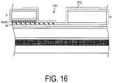
In this regard, in the case that a layered film of Al (lower film) and MoN (upper film), for example, is used as the first metal film and ITO, for example, is used as the second metal film, as illustrated in FIG. 16, the upper film (MoN) of the first metal film may be etched in the etching step for forming the contact hole CH in the interlayer insulating film, and as a result, the lower film (Al) of the first metal film and ITO (second metal film) may come into contact with each other within the contact hole and electrolytic corrosion may occur between the films, which may result in a contact failure.
In the configuration of the first embodiment, even when, for example, aluminum is used in the lower film 9 x of the first metal film and ITO is used in the second metal film, electrolytic corrosion is unlikely to occur because the films are not in contact with each other. Hence, this configuration prevents the occurrence of a contact failure due to electrolytic corrosion.
Second Embodiment
The second embodiment is configured as illustrated in FIGS. 7A and 7B, in comparison with the configuration illustrated in FIGS. 5A and 5B.
As illustrated in FIG. 7A, at the bottom of the contact hole CH provided in the interlayer insulating film F, the conductive film 7 c (overlapping portion overlapping with the contact hole) is in contact with the second metal film 12, and the films are electrically connected to each other. The conductive film 7 c of FIGS. 7A and 7B is a film obtained by performing a plasma treatment on a semiconductor film formed in the same layer (in the same process) as the oxide semiconductor film 7 s of FIGS. 4A and 4B and thus converting the film into a conductor.
Outside of the bottom of the contact hole CH, the perimeter portion (non-overlapping portion not overlapping with the contact hole) of the conductive film 7 c and an end portion 9E of the first metal film 9 are in contact with each other and thus electrically connected to each other. In FIG. 7A, as opposed to FIG. 5A, the interlayer insulating film F is not formed between the end face 9F of the first metal film and a portion of the second metal film 12 within the contact hole CH, and thus a cavity is present therebetween.
The configuration of FIGS. 7A and 7B can be formed as illustrated in FIG. 8. Steps S1 to S7 are the same as those in FIG. 6. In step S8, the film of the first metal film 9 (e.g., a layered film of the lower film 9 x including Al and the upper film 9 y including MoN) is formed and patterned.
Here, as illustrated in FIG. 9A, the end portion 9 e of the first metal film 9 is placed on the perimeter portion (portion extending beyond the contact region CR) of the oxide semiconductor film 7 s, and the end face 9 f of the first metal film 9 is positioned on or inside the edge of the contact region CR.
In step S9, the film of the first passivation film 10 a is formed. In step S10, the film of the upper transparent film 11 is formed. In step S11, the film of the second passivation film 10 b is formed.
In step S12, the film of the interlayer insulating film F is formed and patterned. Here, the contact hole CH is formed in the interlayer insulating film F at the portion on the contact region CR, and thus the oxide semiconductor film 7 s is exposed at the bottom of the contact hole CH.
In step S13, the first metal film 9 (9 x, 9 y) is etched by wet etching, and thus, as illustrated in FIG. 9B, the end face 9F of the first metal film 9 is retracted away from the edge (position of the side wall) of the contact region CR so that the end face 9F of the first metal film 9 can be located outside of the contact region CR and the end portion 9E of the first metal film 9 can overlap with the oxide semiconductor film 7 s (the lower film 9 x can be in contact with the oxide semiconductor film 7 s).
In step S14, a plasma treatment is performed on the oxide semiconductor film 7 s at the contact region CR by using, for example, argon, hydrogen, or the like, other than oxygen. Thus, in the oxide semiconductor film 7 s overlapping with the contact region CR, the portion overlapping with the end portion 9E of the first metal film 9 and the portion extending from the overlapping portion to the bottom of the contact hole CH (portion on which the interlayer insulating film F is not formed) as well as the portion exposed at the bottom of the contact hole CH are converted into a conductor to form the conductive film 7 c. Thus, the conductive film 7 c is electrically connected to the first metal film 9 (lower film 9 x).
In the configuration of the second embodiment, even when, for example, aluminum is used in the lower film 9 x of the first metal film and ITO is used in the second metal film, electrolytic corrosion is unlikely to occur because the films are not in contact with each other. Hence, this configuration prevents the occurrence of a contact failure due to electrolytic corrosion.
In the configuration of FIGS. 7A and 7B, the interlayer insulating film F is not present in the gap (there is a cavity) between the end face 9F of the first metal film 9 and the edge (position of the side wall) of the contact hole CH, and thus the portion of the oxide semiconductor film under the gap can be easily converted into a conductor by performing a plasma treatment. Accordingly, the gap can be configured to be greater than the thickness of the interlayer insulating film F, and the alignment of the oxide semiconductor film 7 s in step S7 becomes easy.
In step S15, the second metal film 12 is formed on the interlayer insulating film F. Here, at the bottom of the contact hole CH, the second metal film 12 comes into contact with the conductive film 7 c to be electrically connected thereto. As a result, the first metal film 9 and the second metal film 12 are electrically connected to each other with the conductive film 7 c therebetween.
In the manner described above, the active matrix substrate 17 of FIGS. 7A and 7B can be formed. Note that, as illustrated in FIG. 7A, the second metal film 12 is disconnected at the side wall portion of the contact hole CH, but the electrical connection to the conductive film 7 c is ensured at the near portion.
Third Embodiment
In the active matrix substrate of each of the first and second embodiments, the configuration of the TFT portion is of the channel etched type, but the configuration is not limited to this. As illustrated in FIG. 10, it is also possible that an etching stopper film 8 is provided. Specifically, the etching stopper film 8 is formed on the oxide semiconductor film 7 s, and the first metal films 9 s, 9 d are formed on the etching stopper film 8. Note that the etching stopper film 8 is formed by, for example, forming the film of a SiO2 film with a PECVD method and patterning the film.
The etching stopper film 8, when provided, prevents the oxide semiconductor film 7 s from being affected by the etching of the first metal film when forming the first metal films 9 s, 9 d.
As illustrated in FIGS. 11 and 12, the third embodiment is also configured as follows. The contact hole CH is provided in the interlayer insulating film F, the interlayer insulating film F being an upper layer over the conductive film 7 c obtained by converting an oxide semiconductor film into a conductor. Within the contact hole CH, the conductive film 7 c is in contact with the second metal film 12 (e.g., a transparent film including ITO). Outside of the contact hole CH, the conductive film 7 c is in contact with the first metal film 9 (e.g., a layered film of the lower film 9 x including Al and the upper film 9 y including MoN).
Note that the configuration may be such that, as illustrated in FIG. 11, a portion of the interlayer insulating film F is present in the gap between the end face 9F of the first metal film 9 and a portion of the second metal film 12 within the contact hole CH or the configuration may be such that, as illustrated in FIG. 12, the interlayer insulating film F is not present in the gap (there is a cavity) between the end face 9F of the first metal film 9 and a portion of the second metal film 12 within the contact hole CH.
Fourth Embodiment
A MEMS display is described in the first embodiment, but the embodiment is not limited thereto. The active matrix substrate of each of the first to third embodiments may be employed in a liquid crystal display device.
As illustrated in FIG. 13A, a liquid crystal display device 100, according to a fourth embodiment includes a liquid crystal panel 67 and a backlight 77. The liquid crystal panel 67 includes an active matrix substrate 27 and a counter substrate (color filter substrate) 37. The backlight 77 emits LED light or laser light to the active matrix substrate 27. As illustrated in FIG. 13B, in a pixel PIX of the liquid crystal panel 67, the pixel electrode of a liquid crystal capacitor LC is connected to a data signal line DS and a scanning signal line SC with a transistor Tr therebetween, and the counter electrode of the liquid crystal capacitor LC is connected to a common electrode line COM.
For the liquid crystal panel 67, an active matrix substrate 27 may be used. As illustrated in FIGS. 14A and 14B, the active matrix substrate 27 corresponds to the active matrix substrate 17 of the first embodiment illustrated in FIGS. 4A to 5B except that the light shielding film 2, the first inorganic insulating film 3 a, the lower transparent film 4, the second inorganic insulating film 3 b, and the third passivation film 10 c are not included. Another active matrix substrate 27 may be used. As illustrated in FIGS. 15A and 15B, the active matrix substrate 27 corresponds to the active matrix substrate 17 of the second embodiment illustrated in FIGS. 4A and 4B and FIGS. 7A and 7B except that the light shielding film 2, the first inorganic insulating film 3 a, the lower transparent film 4, the second inorganic insulating film 3 b, and the third passivation film 10 c are not included.
First to Fourth Embodiments
In the active matrix substrate of each of the first to fourth embodiments, the first metal film 9 and the second metal film 12 are electrically connected to each other. The layer in which each of the metal films is to be formed is not limited to the configuration of any of the embodiments. The active matrix substrate according to an embodiment of the disclosure may be employed in display devices in general that include an active matrix substrate having a configuration in which two metal films formed in different layers are electrically connected to each other (and particularly in which electrolytic corrosion may occur in a case where the metal films contact each other). The active matrix substrate is also suitable for organic electroluminescence (organic EL) displays and inorganic electroluminescence (inorganic EL) displays.
Supplement
According to a first aspect of the disclosure, an active matrix substrate includes a substrate, a first metal film and an interlayer insulating film, and a second metal film. The interlayer insulating film is formed in an upper layer on the first metal film. The second metal film is formed in the upper layer on the interlayer insulating film. The first metal film and the second metal film are electrically connected to each other via a contact hole formed in the interlayer insulating film. An oxide semiconductor film converted into a conductor is provided in a layer between the substrate and the first metal film. Within the contact hole, the oxide semiconductor film converted into a conductor is in contact with the second metal film. Outside of the contact hole, the oxide semiconductor film converted into a conductor is in contact with the first metal film.
According to a second aspect of the disclosure, the active matrix substrate is configured as follows. In the first aspect, the first metal film does not overlap with the contact hole.
According to a third aspect of the disclosure, the active matrix substrate is configured as follows. In the first or second aspect, the oxide semiconductor film converted into a conductor overlaps with the entirety of the inner region of the contact hole.
According to a fourth aspect of the disclosure, the active matrix substrate is configured as follows. In the second aspect, an end portion of the first metal film includes an end face facing a side wall of the contact hole, and a distance from the end face to the side wall of the contact hole is less than a thickness of the interlayer insulating film.
According to a fifth aspect of the disclosure, the active matrix substrate is configured as follows. In the second aspect, an end portion of the first metal film is located away from the contact hole, and a cavity is formed between the end portion of the first metal film and a portion of the second metal film within the contact hole.
According to a sixth aspect of the disclosure, the active matrix substrate is configured as follows. In any one of the first to fifth aspects, the second metal film includes a transparent metal film.
According to a seventh aspect of the disclosure, the active matrix substrate is configured as follows. In any one of the first to sixth aspects, the oxide semiconductor film converted into a conductor includes a conductive film formed in a layer identical to a layer in which an oxide semiconductor film serving as a channel of a transistor is formed.
According to an eighth aspect of the disclosure, the active matrix substrate is configured as follows. In any one of the first to seventh aspects, the first metal film includes aluminum.
According to a ninth aspect of the disclosure, an optical shutter substrate includes the active matrix substrate according to any one of the first to eighth aspects and an optical shutter mechanism formed on the active matrix substrate.
According to a tenth aspect of the disclosure, a display device includes the active matrix substrate according to any one of the first to eighth aspects.
According to an eleventh aspect of the disclosure, a method for manufacturing an active matrix substrate includes first to sixth steps. In the first step, an oxide semiconductor film is formed. In the second step, a first metal film is formed in an upper layer on the oxide semiconductor film. In the third step, an interlayer insulating film is formed in an upper layer on the first metal film. In the fourth step, a contact hole is formed in the interlayer insulating film to expose a portion of the oxide semiconductor film. In the fifth step, a plasma treatment is performed on the oxide semiconductor film, and the oxide semiconductor film is converted into a conductive film. In the sixth step, a second metal film is formed such that the second metal film covers a portion of the conductive film within the contact hole.
According to a twelfth aspect of the disclosure, the method for manufacturing an active matrix substrate includes the following technique. In the eleventh aspect, in the second step, the first metal film is formed such that the first metal film does not overlap with a location where the contact hole is to be formed and such that the first metal film is in contact with the oxide semiconductor film.
According to a thirteenth aspect of the disclosure, the method for manufacturing an active matrix substrate includes the following technique. In the eleventh aspect, in the second step, the first metal film is formed such that the first metal film overlaps with a location where the contact hole is to be formed and such that the first metal film is in contact with the oxide semiconductor film, and, between the fourth step and the fifth step, the first metal film is etched such that the first metal film is in contact with the oxide semiconductor film but does not overlap with the contact hole.
The disclosure is not limited to the embodiments stated above, and various modifications may be implemented within a range not departing from the scope of the claims. Embodiments obtained by appropriately combining technical approaches stated in each of the different embodiments also fall within the scope of the technology of the disclosure. Moreover, novel technical features may be formed by combining the technical approaches stated in each of the embodiments.
REFERENCE SIGNS LIST
  • 1 Glass substrate
  • 2 Light shielding film
  • 4 Lower transparent film
  • 5 Lower metal film
  • 6 Gate insulating film
  • 7 Oxide semiconductor film
  • 7 s Oxide semiconductor film
  • 7 c Conductive film (oxide semiconductor film converted into conductor)
  • 9 First metal film
  • 10 a to 10 c First to third passivation films
  • 11 Upper transparent film
  • 12 Second metal film
  • 13 Upper metal film
  • 17 Active matrix substrate
  • 20 Optical shutter substrate
  • 21 Optical shutter mechanism
  • 22 x, 22 y Drive beam
  • 23 x, 23 y Shutter beam
  • 27 Active matrix substrate
  • 28 Shutter body
  • 30 Counter substrate
  • LW Light transmission path
  • F Interlayer insulating film

Claims (9)

The invention claimed is:
1. An active matrix substrate comprising:
a substrate;
a first metal film;
an interlayer insulating film formed in an upper layer on the first metal film; and
a second metal film formed in an upper layer on the interlayer insulating film, the first metal film and the second metal film being electrically connected to each other via a contact hole formed in the interlayer insulating film,
wherein an oxide semiconductor film converted into a conductor is provided in a layer between the substrate and the first metal film,
within the contact hole, the oxide semiconductor film converted into a conductor is in contact with the second metal film,
outside of the contact hole, the oxide semiconductor film converted into a conductor is in contact with the first metal film,
the first metal film does not overlap with the contact hole,
an end portion of the first metal film includes an end face facing a side wall of the contact hole, and
a distance from the end face to the side wall of the contact hole is less than a thickness of the interlayer insulating film.
2. The active matrix substrate according to claim 1,
wherein the oxide semiconductor film converted into a conductor overlaps with an entirety of an inner region of the contact hole.
3. The active matrix substrate according to claim 1,
wherein an end portion of the first metal film is located away from the contact hole, and a cavity is formed between the end portion of the first metal film and a portion of the second metal film within the contact hole.
4. The active matrix substrate according to claim 1,
wherein the second metal film includes a transparent metal film.
5. The active matrix substrate according to claim 1,
wherein the oxide semiconductor film converted into a conductor includes a conductive film formed in a layer identical to a layer in which an oxide semiconductor film serving as a channel of a transistor is formed.
6. The active matrix substrate according to claim 1,
wherein the first metal film includes aluminum.
7. An optical shutter substrate comprising:
the active matrix substrate according to claim 1; and
an optical shutter mechanism formed on the active matrix substrate.
8. A display device comprising the active matrix substrate according to claim 1.
9. A method for manufacturing an active matrix substrate, the method comprising:
a first step of forming an oxide semiconductor film;
a second step of forming a first metal film in an upper layer on the oxide semiconductor film;
a third step of forming an interlayer insulating film in an upper layer on the first metal film;
a fourth step of forming a contact hole in the interlayer insulating film to expose a portion of the oxide semiconductor film;
a fifth step of performing a plasma treatment on the oxide semiconductor film and converting the oxide semiconductor film into a conductive film; and
a sixth step of forming a second metal film such that the second metal film covers a portion of the conductive film within the contact hole; wherein
in the second step, the first metal film is formed such that the first metal film overlaps with a location where the contact hole is to be formed and such that the first metal film is in contact with the oxide semiconductor film, and
between the fourth step and the fifth step, the first metal film is etched such that the first metal film is in contact with the oxide semiconductor film but does not overlap with the contact hole.
US16/305,417 2016-06-23 2017-06-16 Active matrix substrate, optical shutter substrate, display device, and method for manufacturing active matrix substrate Active 2038-05-27 US10991729B2 (en)

Applications Claiming Priority (4)

Application Number Priority Date Filing Date Title
JPJP2016-124791 2016-06-23
JP2016124791 2016-06-23
JP2016-124791 2016-06-23
PCT/JP2017/022245 WO2017221815A1 (en) 2016-06-23 2017-06-16 Active matrix substrate, optical shutter substrate, display device and method for producing active matrix substrate

Publications (2)

Publication Number Publication Date
US20200328235A1 US20200328235A1 (en) 2020-10-15
US10991729B2 true US10991729B2 (en) 2021-04-27

Family

ID=60784732

Family Applications (1)

Application Number Title Priority Date Filing Date
US16/305,417 Active 2038-05-27 US10991729B2 (en) 2016-06-23 2017-06-16 Active matrix substrate, optical shutter substrate, display device, and method for manufacturing active matrix substrate

Country Status (2)

Country Link
US (1) US10991729B2 (en)
WO (1) WO2017221815A1 (en)

Citations (8)

* Cited by examiner, † Cited by third party
Publication number Priority date Publication date Assignee Title
US20080035920A1 (en) 2006-08-09 2008-02-14 Nec Corporation Thin-film transistor array, method of fabricating the same, and liquid crystal display device including the same
EP1859311B1 (en) 2005-02-23 2008-11-19 Pixtronix Inc. Light modulator and method for manufature thereof
US20100090942A1 (en) * 2008-10-10 2010-04-15 Tpo Displays Corp. Active matrix display device
US20150162399A1 (en) 2013-12-05 2015-06-11 Sony Corporation Semiconductor device, method of manufacturing the same, display unit, and electronic apparatus
WO2015087586A1 (en) 2013-12-10 2015-06-18 シャープ株式会社 Semiconductor device and method for manufacturing same
US20160104759A1 (en) 2014-10-10 2016-04-14 Sony Corporation Display unit and electronic apparatus
JP2016057547A (en) 2014-09-11 2016-04-21 シャープ株式会社 MEMS display and manufacturing method thereof
US20170287943A1 (en) * 2016-03-31 2017-10-05 Qualcomm Incorporated High aperture ratio display by introducing transparent storage capacitor and via hole

Family Cites Families (3)

* Cited by examiner, † Cited by third party
Publication number Priority date Publication date Assignee Title
CN103053014B (en) * 2010-08-07 2016-03-16 夏普株式会社 Thin film transistor base plate and the liquid crystal indicator possessing it
WO2013115043A1 (en) * 2012-01-31 2013-08-08 シャープ株式会社 Display device
JP2014081416A (en) * 2012-10-15 2014-05-08 Japan Display Inc Aperture plate and display device with the same

Patent Citations (13)

* Cited by examiner, † Cited by third party
Publication number Priority date Publication date Assignee Title
EP1859311B1 (en) 2005-02-23 2008-11-19 Pixtronix Inc. Light modulator and method for manufature thereof
JP2011043856A (en) 2005-02-23 2011-03-03 Pixtronix Inc Display device and method for manufacturing the same
US20080035920A1 (en) 2006-08-09 2008-02-14 Nec Corporation Thin-film transistor array, method of fabricating the same, and liquid crystal display device including the same
JP2008040343A (en) 2006-08-09 2008-02-21 Nec Corp Thin film transistor array, manufacturing method thereof, and liquid crystal display device
US20100090942A1 (en) * 2008-10-10 2010-04-15 Tpo Displays Corp. Active matrix display device
JP2015108731A (en) 2013-12-05 2015-06-11 ソニー株式会社 Semiconductor device and manufacturing method thereof, and display device and electronic apparatus
US20150162399A1 (en) 2013-12-05 2015-06-11 Sony Corporation Semiconductor device, method of manufacturing the same, display unit, and electronic apparatus
WO2015087586A1 (en) 2013-12-10 2015-06-18 シャープ株式会社 Semiconductor device and method for manufacturing same
US20160380006A1 (en) 2013-12-10 2016-12-29 Sharp Kabushiki Kaisha Semiconductor device and method for manufacturing same
JP2016057547A (en) 2014-09-11 2016-04-21 シャープ株式会社 MEMS display and manufacturing method thereof
US20160104759A1 (en) 2014-10-10 2016-04-14 Sony Corporation Display unit and electronic apparatus
JP2016080744A (en) 2014-10-10 2016-05-16 株式会社Joled Display device and electronic apparatus
US20170287943A1 (en) * 2016-03-31 2017-10-05 Qualcomm Incorporated High aperture ratio display by introducing transparent storage capacitor and via hole

Non-Patent Citations (1)

* Cited by examiner, † Cited by third party
Title
Official Communication issued in International Patent Application No. PCT/JP2017/022245, dated Aug. 29, 2017.

Also Published As

Publication number Publication date
US20200328235A1 (en) 2020-10-15
WO2017221815A1 (en) 2017-12-28

Similar Documents

Publication Publication Date Title
US11322105B2 (en) Active matrix substrate, liquid crystal display device, and organic EL display device
US10451946B2 (en) Semiconductor device, liquid crystal display device, and semiconductor device manufacturing method
US10656483B2 (en) Semiconductor apparatus and method for manufacturing semiconductor apparatus
KR102089244B1 (en) Double gate type thin film transistor and organic light emitting diode display device including the same
US9142682B2 (en) Thin film transistor and manufacturing method thereof
US20160181291A1 (en) Semiconductor device, display device, and method for manufacturing semiconductor device
US20180204853A1 (en) Active matrix substrate and method for producing same, and in-cell touch panel-type display device
KR20210088564A (en) semiconductor device
US10283645B2 (en) Semiconductor device and method for manufacturing same
US10670933B2 (en) Active matrix substrate, method for producing same, and display device
US11024656B2 (en) Active matrix substrate, optical shutter substrate, display device, and method for manufacturing active matrix substrate
US10651209B2 (en) Semiconductor device and method for manufacturing same
WO2017007004A1 (en) Active matrix substrate, display device and method for manufacturing display device
CN108780221B (en) Display panel, display device, and manufacturing method of display panel
WO2017007002A1 (en) Active matrix substrate, display device, and manufacturing method
US9716183B2 (en) Semiconductor device and method of manufacturing same
US9690155B2 (en) Liquid crystal display panel and method for producing same
US10991729B2 (en) Active matrix substrate, optical shutter substrate, display device, and method for manufacturing active matrix substrate
US20150048360A1 (en) Semiconductor device and semiconductor device manufacturing method
KR102132412B1 (en) Thin fim transistor array substrate for display device and method fabricating the same
CN107851406A (en) Active-matrix substrate, display device and manufacture method
US20140252355A1 (en) Semiconductor device and method for producing same
KR20160049172A (en) Thin film transistor array substrate and display device comprising the same
JP2017181953A (en) Optical shutter substrate, printer head
JP2017191297A (en) Optical shutter substrate, printer head

Legal Events

Date Code Title Description
AS Assignment

Owner name: SHARP KABUSHIKI KAISHA, JAPAN

Free format text: ASSIGNMENT OF ASSIGNORS INTEREST;ASSIGNORS:OKABE, TOHRU;NISHIKI, HIROHIKO;YANEDA, TAKESHI;SIGNING DATES FROM 20181017 TO 20181023;REEL/FRAME:047618/0225

FEPP Fee payment procedure

Free format text: ENTITY STATUS SET TO UNDISCOUNTED (ORIGINAL EVENT CODE: BIG.); ENTITY STATUS OF PATENT OWNER: LARGE ENTITY

STPP Information on status: patent application and granting procedure in general

Free format text: DOCKETED NEW CASE - READY FOR EXAMINATION

STPP Information on status: patent application and granting procedure in general

Free format text: NOTICE OF ALLOWANCE MAILED -- APPLICATION RECEIVED IN OFFICE OF PUBLICATIONS

STPP Information on status: patent application and granting procedure in general

Free format text: PUBLICATIONS -- ISSUE FEE PAYMENT RECEIVED

STPP Information on status: patent application and granting procedure in general

Free format text: PUBLICATIONS -- ISSUE FEE PAYMENT VERIFIED

STCF Information on status: patent grant

Free format text: PATENTED CASE

MAFP Maintenance fee payment

Free format text: PAYMENT OF MAINTENANCE FEE, 4TH YEAR, LARGE ENTITY (ORIGINAL EVENT CODE: M1551); ENTITY STATUS OF PATENT OWNER: LARGE ENTITY

Year of fee payment: 4