US10978642B2 - Mixture, composition and organic electronic device - Google Patents
Mixture, composition and organic electronic device Download PDFInfo
- Publication number
- US10978642B2 US10978642B2 US16/467,413 US201716467413A US10978642B2 US 10978642 B2 US10978642 B2 US 10978642B2 US 201716467413 A US201716467413 A US 201716467413A US 10978642 B2 US10978642 B2 US 10978642B2
- Authority
- US
- United States
- Prior art keywords
- derivative
- organic
- group containing
- organic compounds
- group
- Prior art date
- Legal status (The legal status is an assumption and is not a legal conclusion. Google has not performed a legal analysis and makes no representation as to the accuracy of the status listed.)
- Active, expires
Links
- 239000000203 mixture Substances 0.000 title claims abstract description 145
- 150000002894 organic compounds Chemical class 0.000 claims abstract description 124
- 239000000463 material Substances 0.000 claims description 110
- 125000001072 heteroaryl group Chemical group 0.000 claims description 54
- 125000003118 aryl group Chemical group 0.000 claims description 52
- 125000006413 ring segment Chemical group 0.000 claims description 51
- -1 hydroxy, carbonyl Chemical group 0.000 claims description 50
- 239000010410 layer Substances 0.000 claims description 49
- 125000004432 carbon atom Chemical group C* 0.000 claims description 44
- 238000009472 formulation Methods 0.000 claims description 44
- 238000004768 lowest unoccupied molecular orbital Methods 0.000 claims description 24
- 238000004770 highest occupied molecular orbital Methods 0.000 claims description 22
- 229910052757 nitrogen Inorganic materials 0.000 claims description 22
- 230000000903 blocking effect Effects 0.000 claims description 20
- BBEAQIROQSPTKN-UHFFFAOYSA-N antipyrene Natural products C1=CC=C2C=CC3=CC=CC4=CC=C1C2=C43 BBEAQIROQSPTKN-UHFFFAOYSA-N 0.000 claims description 16
- 230000005281 excited state Effects 0.000 claims description 15
- JUJWROOIHBZHMG-UHFFFAOYSA-N Pyridine Chemical compound C1=CC=NC=C1 JUJWROOIHBZHMG-UHFFFAOYSA-N 0.000 claims description 14
- 125000000217 alkyl group Chemical group 0.000 claims description 14
- 238000002347 injection Methods 0.000 claims description 14
- 239000007924 injection Substances 0.000 claims description 14
- 229910052717 sulfur Inorganic materials 0.000 claims description 14
- 229910052739 hydrogen Inorganic materials 0.000 claims description 13
- 229910052760 oxygen Inorganic materials 0.000 claims description 13
- 125000003545 alkoxy group Chemical group 0.000 claims description 12
- 239000003960 organic solvent Substances 0.000 claims description 12
- IOJUPLGTWVMSFF-UHFFFAOYSA-N benzothiazole Chemical class C1=CC=C2SC=NC2=C1 IOJUPLGTWVMSFF-UHFFFAOYSA-N 0.000 claims description 11
- GVEPBJHOBDJJJI-UHFFFAOYSA-N fluoranthrene Natural products C1=CC(C2=CC=CC=C22)=C3C2=CC=CC3=C1 GVEPBJHOBDJJJI-UHFFFAOYSA-N 0.000 claims description 11
- 150000001412 amines Chemical class 0.000 claims description 10
- 230000005669 field effect Effects 0.000 claims description 9
- 239000002346 layers by function Substances 0.000 claims description 9
- 229910052805 deuterium Inorganic materials 0.000 claims description 8
- 238000009835 boiling Methods 0.000 claims description 7
- 229910052799 carbon Inorganic materials 0.000 claims description 7
- 125000002924 primary amino group Chemical group [H]N([H])* 0.000 claims description 7
- BCMCBBGGLRIHSE-UHFFFAOYSA-N 1,3-benzoxazole Chemical class C1=CC=C2OC=NC2=C1 BCMCBBGGLRIHSE-UHFFFAOYSA-N 0.000 claims description 6
- ZOXJGFHDIHLPTG-UHFFFAOYSA-N Boron Chemical compound [B] ZOXJGFHDIHLPTG-UHFFFAOYSA-N 0.000 claims description 6
- 125000002252 acyl group Chemical group 0.000 claims description 6
- 125000003342 alkenyl group Chemical group 0.000 claims description 6
- 125000000304 alkynyl group Chemical group 0.000 claims description 6
- 229910052796 boron Inorganic materials 0.000 claims description 6
- 125000000753 cycloalkyl group Chemical group 0.000 claims description 6
- 229910052731 fluorine Inorganic materials 0.000 claims description 6
- 230000005693 optoelectronics Effects 0.000 claims description 6
- 125000000472 sulfonyl group Chemical group *S(*)(=O)=O 0.000 claims description 6
- ICPSWZFVWAPUKF-UHFFFAOYSA-N 1,1'-spirobi[fluorene] Chemical class C1=CC=C2C=C3C4(C=5C(C6=CC=CC=C6C=5)=CC=C4)C=CC=C3C2=C1 ICPSWZFVWAPUKF-UHFFFAOYSA-N 0.000 claims description 5
- 125000004093 cyano group Chemical group *C#N 0.000 claims description 5
- 230000003111 delayed effect Effects 0.000 claims description 5
- 125000003983 fluorenyl group Chemical class C1(=CC=CC=2C3=CC=CC=C3CC12)* 0.000 claims description 5
- 125000000449 nitro group Chemical group [O-][N+](*)=O 0.000 claims description 5
- 238000000859 sublimation Methods 0.000 claims description 5
- 230000008022 sublimation Effects 0.000 claims description 5
- 125000002915 carbonyl group Chemical group [*:2]C([*:1])=O 0.000 claims description 4
- 125000001183 hydrocarbyl group Chemical group 0.000 claims description 4
- 150000002825 nitriles Chemical class 0.000 claims description 4
- 238000013086 organic photovoltaic Methods 0.000 claims description 4
- 150000002987 phenanthrenes Chemical class 0.000 claims description 4
- 150000003220 pyrenes Chemical class 0.000 claims description 4
- 125000002023 trifluoromethyl group Chemical group FC(F)(F)* 0.000 claims description 4
- GOLORTLGFDVFDW-UHFFFAOYSA-N 3-(1h-benzimidazol-2-yl)-7-(diethylamino)chromen-2-one Chemical class C1=CC=C2NC(C3=CC4=CC=C(C=C4OC3=O)N(CC)CC)=NC2=C1 GOLORTLGFDVFDW-UHFFFAOYSA-N 0.000 claims description 3
- FBXGQDUVJBKEAJ-UHFFFAOYSA-N 4h-oxazin-3-one Chemical class O=C1CC=CON1 FBXGQDUVJBKEAJ-UHFFFAOYSA-N 0.000 claims description 3
- NRCMAYZCPIVABH-UHFFFAOYSA-N Quinacridone Chemical class N1C2=CC=CC=C2C(=O)C2=C1C=C1C(=O)C3=CC=CC=C3NC1=C2 NRCMAYZCPIVABH-UHFFFAOYSA-N 0.000 claims description 3
- 150000001556 benzimidazoles Chemical class 0.000 claims description 3
- VPUGDVKSAQVFFS-UHFFFAOYSA-N coronene Chemical class C1=C(C2=C34)C=CC3=CC=C(C=C3)C4=C4C3=CC=C(C=C3)C4=C2C3=C1 VPUGDVKSAQVFFS-UHFFFAOYSA-N 0.000 claims description 3
- SIFHTIHFPPIGBL-UHFFFAOYSA-N ctk2i0750 Chemical class C12=C3C4=CC=CC3=CC=C2C=CC=C1C1=C4CC2=CC=CC=C21 SIFHTIHFPPIGBL-UHFFFAOYSA-N 0.000 claims description 3
- ZSWFCLXCOIISFI-UHFFFAOYSA-N cyclopentadiene Chemical class C1C=CC=C1 ZSWFCLXCOIISFI-UHFFFAOYSA-N 0.000 claims description 3
- 125000002462 isocyano group Chemical group *[N+]#[C-] 0.000 claims description 3
- 150000002790 naphthalenes Chemical class 0.000 claims description 3
- 125000000843 phenylene group Chemical group C1(=C(C=CC=C1)*)* 0.000 claims description 3
- FYNROBRQIVCIQF-UHFFFAOYSA-N pyrrolo[3,2-b]pyrrole-5,6-dione Chemical class C1=CN=C2C(=O)C(=O)N=C21 FYNROBRQIVCIQF-UHFFFAOYSA-N 0.000 claims description 3
- PYWVYCXTNDRMGF-UHFFFAOYSA-N rhodamine B Chemical class [Cl-].C=12C=CC(=[N+](CC)CC)C=C2OC2=CC(N(CC)CC)=CC=C2C=1C1=CC=CC=C1C(O)=O PYWVYCXTNDRMGF-UHFFFAOYSA-N 0.000 claims description 3
- YYMBJDOZVAITBP-UHFFFAOYSA-N rubrene Chemical class C1=CC=CC=C1C(C1=C(C=2C=CC=CC=2)C2=CC=CC=C2C(C=2C=CC=CC=2)=C11)=C(C=CC=C2)C2=C1C1=CC=CC=C1 YYMBJDOZVAITBP-UHFFFAOYSA-N 0.000 claims description 3
- 150000004882 thiopyrans Chemical class 0.000 claims description 3
- 229920002554 vinyl polymer Polymers 0.000 claims description 3
- 150000001408 amides Chemical class 0.000 claims description 2
- 239000012298 atmosphere Substances 0.000 claims description 2
- 150000003949 imides Chemical class 0.000 claims description 2
- 230000031700 light absorption Effects 0.000 claims description 2
- 125000000325 methylidene group Chemical group [H]C([H])=* 0.000 claims description 2
- 150000007660 quinolones Chemical class 0.000 claims description 2
- 150000003518 tetracenes Chemical class 0.000 claims description 2
- JCXJVPUVTGWSNB-UHFFFAOYSA-N Nitrogen dioxide Chemical compound O=[N]=O JCXJVPUVTGWSNB-UHFFFAOYSA-N 0.000 claims 1
- 125000004309 pyranyl group Chemical class O1C(C=CC=C1)* 0.000 claims 1
- 125000001834 xanthenyl group Chemical class C1=CC=CC=2OC3=CC=CC=C3C(C12)* 0.000 claims 1
- 0 *c(cc1c2c3c(-c4cccc(c5c6ccc(*)c5)c4[n]6-c4cc(-c5ccccc5)cc(-c5ccccc5)c4)ccc2)ccc1[n]3-c1ccccc1 Chemical compound *c(cc1c2c3c(-c4cccc(c5c6ccc(*)c5)c4[n]6-c4cc(-c5ccccc5)cc(-c5ccccc5)c4)ccc2)ccc1[n]3-c1ccccc1 0.000 description 24
- YXFVVABEGXRONW-UHFFFAOYSA-N Toluene Chemical compound CC1=CC=CC=C1 YXFVVABEGXRONW-UHFFFAOYSA-N 0.000 description 24
- 239000000758 substrate Substances 0.000 description 22
- 229910052751 metal Inorganic materials 0.000 description 20
- 239000002184 metal Substances 0.000 description 20
- YTPLMLYBLZKORZ-UHFFFAOYSA-N Thiophene Chemical compound C=1C=CSC=1 YTPLMLYBLZKORZ-UHFFFAOYSA-N 0.000 description 18
- 150000001875 compounds Chemical class 0.000 description 16
- RAXXELZNTBOGNW-UHFFFAOYSA-N imidazole Natural products C1=CNC=N1 RAXXELZNTBOGNW-UHFFFAOYSA-N 0.000 description 15
- IJGRMHOSHXDMSA-UHFFFAOYSA-N Atomic nitrogen Chemical compound N#N IJGRMHOSHXDMSA-UHFFFAOYSA-N 0.000 description 14
- RTZKZFJDLAIYFH-UHFFFAOYSA-N Diethyl ether Chemical compound CCOCC RTZKZFJDLAIYFH-UHFFFAOYSA-N 0.000 description 14
- UFWIBTONFRDIAS-UHFFFAOYSA-N Naphthalene Chemical compound C1=CC=CC2=CC=CC=C21 UFWIBTONFRDIAS-UHFFFAOYSA-N 0.000 description 14
- SMWDFEZZVXVKRB-UHFFFAOYSA-N Quinoline Chemical compound N1=CC=CC2=CC=CC=C21 SMWDFEZZVXVKRB-UHFFFAOYSA-N 0.000 description 14
- 239000003446 ligand Substances 0.000 description 14
- 238000007639 printing Methods 0.000 description 14
- 150000004982 aromatic amines Chemical class 0.000 description 13
- 125000004122 cyclic group Chemical group 0.000 description 13
- 239000000243 solution Substances 0.000 description 13
- MWPLVEDNUUSJAV-UHFFFAOYSA-N anthracene Chemical compound C1=CC=CC2=CC3=CC=CC=C3C=C21 MWPLVEDNUUSJAV-UHFFFAOYSA-N 0.000 description 12
- 238000000034 method Methods 0.000 description 12
- 238000002360 preparation method Methods 0.000 description 11
- 239000002904 solvent Substances 0.000 description 11
- UJOBWOGCFQCDNV-UHFFFAOYSA-N 9H-carbazole Chemical compound C1=CC=C2C3=CC=CC=C3NC2=C1 UJOBWOGCFQCDNV-UHFFFAOYSA-N 0.000 description 10
- PCNDJXKNXGMECE-UHFFFAOYSA-N Phenazine Natural products C1=CC=CC2=NC3=CC=CC=C3N=C21 PCNDJXKNXGMECE-UHFFFAOYSA-N 0.000 description 10
- KYQCOXFCLRTKLS-UHFFFAOYSA-N Pyrazine Chemical compound C1=CN=CC=N1 KYQCOXFCLRTKLS-UHFFFAOYSA-N 0.000 description 10
- DZBUGLKDJFMEHC-UHFFFAOYSA-N acridine Chemical compound C1=CC=CC2=CC3=CC=CC=C3N=C21 DZBUGLKDJFMEHC-UHFFFAOYSA-N 0.000 description 10
- WDECIBYCCFPHNR-UHFFFAOYSA-N chrysene Chemical compound C1=CC=CC2=CC=C3C4=CC=CC=C4C=CC3=C21 WDECIBYCCFPHNR-UHFFFAOYSA-N 0.000 description 10
- NIHNNTQXNPWCJQ-UHFFFAOYSA-N fluorene Chemical compound C1=CC=C2CC3=CC=CC=C3C2=C1 NIHNNTQXNPWCJQ-UHFFFAOYSA-N 0.000 description 10
- AWJUIBRHMBBTKR-UHFFFAOYSA-N isoquinoline Chemical compound C1=NC=CC2=CC=CC=C21 AWJUIBRHMBBTKR-UHFFFAOYSA-N 0.000 description 10
- XSCHRSMBECNVNS-UHFFFAOYSA-N quinoxaline Chemical compound N1=CC=NC2=CC=CC=C21 XSCHRSMBECNVNS-UHFFFAOYSA-N 0.000 description 10
- 125000005504 styryl group Chemical group 0.000 description 10
- YLQBMQCUIZJEEH-UHFFFAOYSA-N Furan Chemical compound C=1C=COC=1 YLQBMQCUIZJEEH-UHFFFAOYSA-N 0.000 description 9
- ZUOUZKKEUPVFJK-UHFFFAOYSA-N diphenyl Chemical compound C1=CC=CC=C1C1=CC=CC=C1 ZUOUZKKEUPVFJK-UHFFFAOYSA-N 0.000 description 9
- 229930192474 thiophene Natural products 0.000 description 9
- FCEHBMOGCRZNNI-UHFFFAOYSA-N 1-benzothiophene Chemical compound C1=CC=C2SC=CC2=C1 FCEHBMOGCRZNNI-UHFFFAOYSA-N 0.000 description 8
- SIKJAQJRHWYJAI-UHFFFAOYSA-N Indole Chemical compound C1=CC=C2NC=CC2=C1 SIKJAQJRHWYJAI-UHFFFAOYSA-N 0.000 description 8
- 125000001931 aliphatic group Chemical group 0.000 description 8
- TXCDCPKCNAJMEE-UHFFFAOYSA-N dibenzofuran Chemical compound C1=CC=C2C3=CC=CC=C3OC2=C1 TXCDCPKCNAJMEE-UHFFFAOYSA-N 0.000 description 8
- IYYZUPMFVPLQIF-UHFFFAOYSA-N dibenzothiophene Chemical compound C1=CC=C2C3=CC=CC=C3SC2=C1 IYYZUPMFVPLQIF-UHFFFAOYSA-N 0.000 description 8
- YNPNZTXNASCQKK-UHFFFAOYSA-N phenanthrene Chemical compound C1=CC=C2C3=CC=CC=C3C=CC2=C1 YNPNZTXNASCQKK-UHFFFAOYSA-N 0.000 description 8
- 238000003775 Density Functional Theory Methods 0.000 description 7
- 125000004429 atom Chemical group 0.000 description 7
- 230000000052 comparative effect Effects 0.000 description 7
- UHOVQNZJYSORNB-UHFFFAOYSA-N Benzene Chemical compound C1=CC=CC=C1 UHOVQNZJYSORNB-UHFFFAOYSA-N 0.000 description 6
- PPBRXRYQALVLMV-UHFFFAOYSA-N Styrene Chemical compound C=CC1=CC=CC=C1 PPBRXRYQALVLMV-UHFFFAOYSA-N 0.000 description 6
- CUFNKYGDVFVPHO-UHFFFAOYSA-N azulene Chemical compound C1=CC=CC2=CC=CC2=C1 CUFNKYGDVFVPHO-UHFFFAOYSA-N 0.000 description 6
- 239000001257 hydrogen Substances 0.000 description 6
- 125000004435 hydrogen atom Chemical class [H]* 0.000 description 6
- VVVPGLRKXQSQSZ-UHFFFAOYSA-N indolo[3,2-c]carbazole Chemical compound C1=CC=CC2=NC3=C4C5=CC=CC=C5N=C4C=CC3=C21 VVVPGLRKXQSQSZ-UHFFFAOYSA-N 0.000 description 6
- 229910052698 phosphorus Inorganic materials 0.000 description 6
- 229920000642 polymer Polymers 0.000 description 6
- 238000004088 simulation Methods 0.000 description 6
- 239000010409 thin film Substances 0.000 description 6
- 150000003852 triazoles Chemical class 0.000 description 6
- JYEUMXHLPRZUAT-UHFFFAOYSA-N 1,2,3-triazine Chemical compound C1=CN=NN=C1 JYEUMXHLPRZUAT-UHFFFAOYSA-N 0.000 description 5
- VEPOHXYIFQMVHW-XOZOLZJESA-N 2,3-dihydroxybutanedioic acid (2S,3S)-3,4-dimethyl-2-phenylmorpholine Chemical compound OC(C(O)C(O)=O)C(O)=O.C[C@H]1[C@@H](OCCN1C)c1ccccc1 VEPOHXYIFQMVHW-XOZOLZJESA-N 0.000 description 5
- WTKZEGDFNFYCGP-UHFFFAOYSA-N Pyrazole Chemical compound C=1C=NNC=1 WTKZEGDFNFYCGP-UHFFFAOYSA-N 0.000 description 5
- CZPWVGJYEJSRLH-UHFFFAOYSA-N Pyrimidine Chemical compound C1=CN=CN=C1 CZPWVGJYEJSRLH-UHFFFAOYSA-N 0.000 description 5
- XUIMIQQOPSSXEZ-UHFFFAOYSA-N Silicon Chemical group [Si] XUIMIQQOPSSXEZ-UHFFFAOYSA-N 0.000 description 5
- 150000001336 alkenes Chemical class 0.000 description 5
- 150000001345 alkine derivatives Chemical class 0.000 description 5
- 229910052782 aluminium Inorganic materials 0.000 description 5
- 239000003849 aromatic solvent Substances 0.000 description 5
- 125000003710 aryl alkyl group Chemical group 0.000 description 5
- 239000004305 biphenyl Substances 0.000 description 5
- 235000010290 biphenyl Nutrition 0.000 description 5
- 238000004364 calculation method Methods 0.000 description 5
- 238000000576 coating method Methods 0.000 description 5
- 238000005516 engineering process Methods 0.000 description 5
- 239000010408 film Substances 0.000 description 5
- 230000009477 glass transition Effects 0.000 description 5
- 125000004404 heteroalkyl group Chemical group 0.000 description 5
- 229960005544 indolocarbazole Drugs 0.000 description 5
- 238000007641 inkjet printing Methods 0.000 description 5
- WCPAKWJPBJAGKN-UHFFFAOYSA-N oxadiazole Chemical compound C1=CON=N1 WCPAKWJPBJAGKN-UHFFFAOYSA-N 0.000 description 5
- 125000002080 perylenyl group Chemical group C1(=CC=C2C=CC=C3C4=CC=CC5=CC=CC(C1=C23)=C45)* 0.000 description 5
- 229910052697 platinum Inorganic materials 0.000 description 5
- PBMFSQRYOILNGV-UHFFFAOYSA-N pyridazine Chemical compound C1=CC=NN=C1 PBMFSQRYOILNGV-UHFFFAOYSA-N 0.000 description 5
- UMJSCPRVCHMLSP-UHFFFAOYSA-N pyridine Natural products COC1=CC=CN=C1 UMJSCPRVCHMLSP-UHFFFAOYSA-N 0.000 description 5
- 239000004065 semiconductor Substances 0.000 description 5
- 229910052710 silicon Inorganic materials 0.000 description 5
- VLLMWSRANPNYQX-UHFFFAOYSA-N thiadiazole Chemical compound C1=CSN=N1.C1=CSN=N1 VLLMWSRANPNYQX-UHFFFAOYSA-N 0.000 description 5
- KTZQTRPPVKQPFO-UHFFFAOYSA-N 1,2-benzoxazole Chemical compound C1=CC=C2C=NOC2=C1 KTZQTRPPVKQPFO-UHFFFAOYSA-N 0.000 description 4
- YJTKZCDBKVTVBY-UHFFFAOYSA-N 1,3-Diphenylbenzene Chemical group C1=CC=CC=C1C1=CC=CC(C=2C=CC=CC=2)=C1 YJTKZCDBKVTVBY-UHFFFAOYSA-N 0.000 description 4
- BNRDGHFESOHOBF-UHFFFAOYSA-N 1-benzoselenophene Chemical compound C1=CC=C2[se]C=CC2=C1 BNRDGHFESOHOBF-UHFFFAOYSA-N 0.000 description 4
- NQMUGNMMFTYOHK-UHFFFAOYSA-N 1-methoxynaphthalene Chemical compound C1=CC=C2C(OC)=CC=CC2=C1 NQMUGNMMFTYOHK-UHFFFAOYSA-N 0.000 description 4
- WJFKNYWRSNBZNX-UHFFFAOYSA-N 10H-phenothiazine Chemical compound C1=CC=C2NC3=CC=CC=C3SC2=C1 WJFKNYWRSNBZNX-UHFFFAOYSA-N 0.000 description 4
- TZMSYXZUNZXBOL-UHFFFAOYSA-N 10H-phenoxazine Chemical compound C1=CC=C2NC3=CC=CC=C3OC2=C1 TZMSYXZUNZXBOL-UHFFFAOYSA-N 0.000 description 4
- HYZJCKYKOHLVJF-UHFFFAOYSA-N 1H-benzimidazole Chemical compound C1=CC=C2NC=NC2=C1 HYZJCKYKOHLVJF-UHFFFAOYSA-N 0.000 description 4
- BAXOFTOLAUCFNW-UHFFFAOYSA-N 1H-indazole Chemical compound C1=CC=C2C=NNC2=C1 BAXOFTOLAUCFNW-UHFFFAOYSA-N 0.000 description 4
- OJVAMHKKJGICOG-UHFFFAOYSA-N 2,5-hexanedione Chemical compound CC(=O)CCC(C)=O OJVAMHKKJGICOG-UHFFFAOYSA-N 0.000 description 4
- QMEQBOSUJUOXMX-UHFFFAOYSA-N 2h-oxadiazine Chemical compound N1OC=CC=N1 QMEQBOSUJUOXMX-UHFFFAOYSA-N 0.000 description 4
- BCHZICNRHXRCHY-UHFFFAOYSA-N 2h-oxazine Chemical compound N1OC=CC=C1 BCHZICNRHXRCHY-UHFFFAOYSA-N 0.000 description 4
- BWCDLEQTELFBAW-UHFFFAOYSA-N 3h-dioxazole Chemical compound N1OOC=C1 BWCDLEQTELFBAW-UHFFFAOYSA-N 0.000 description 4
- GJCOSYZMQJWQCA-UHFFFAOYSA-N 9H-xanthene Chemical compound C1=CC=C2CC3=CC=CC=C3OC2=C1 GJCOSYZMQJWQCA-UHFFFAOYSA-N 0.000 description 4
- IYTXKIXETAELAV-UHFFFAOYSA-N Aethyl-n-hexyl-keton Natural products CCCCCCC(=O)CC IYTXKIXETAELAV-UHFFFAOYSA-N 0.000 description 4
- CTQNGGLPUBDAKN-UHFFFAOYSA-N O-Xylene Chemical group CC1=CC=CC=C1C CTQNGGLPUBDAKN-UHFFFAOYSA-N 0.000 description 4
- URLKBWYHVLBVBO-UHFFFAOYSA-N Para-Xylene Chemical group CC1=CC=C(C)C=C1 URLKBWYHVLBVBO-UHFFFAOYSA-N 0.000 description 4
- KAESVJOAVNADME-UHFFFAOYSA-N Pyrrole Chemical compound C=1C=CNC=1 KAESVJOAVNADME-UHFFFAOYSA-N 0.000 description 4
- FZWLAAWBMGSTSO-UHFFFAOYSA-N Thiazole Chemical compound C1=CSC=N1 FZWLAAWBMGSTSO-UHFFFAOYSA-N 0.000 description 4
- RFRXIWQYSOIBDI-UHFFFAOYSA-N benzarone Chemical compound CCC=1OC2=CC=CC=C2C=1C(=O)C1=CC=C(O)C=C1 RFRXIWQYSOIBDI-UHFFFAOYSA-N 0.000 description 4
- 125000005605 benzo group Chemical group 0.000 description 4
- WCZVZNOTHYJIEI-UHFFFAOYSA-N cinnoline Chemical compound N1=NC=CC2=CC=CC=C21 WCZVZNOTHYJIEI-UHFFFAOYSA-N 0.000 description 4
- 229910052802 copper Inorganic materials 0.000 description 4
- ZAJNGDIORYACQU-UHFFFAOYSA-N decan-2-one Chemical compound CCCCCCCCC(C)=O ZAJNGDIORYACQU-UHFFFAOYSA-N 0.000 description 4
- DHFABSXGNHDNCO-UHFFFAOYSA-N dibenzoselenophene Chemical compound C1=CC=C2C3=CC=CC=C3[se]C2=C1 DHFABSXGNHDNCO-UHFFFAOYSA-N 0.000 description 4
- MHDVGSVTJDSBDK-UHFFFAOYSA-N dibenzyl ether Chemical compound C=1C=CC=CC=1COCC1=CC=CC=C1 MHDVGSVTJDSBDK-UHFFFAOYSA-N 0.000 description 4
- 239000011521 glass Substances 0.000 description 4
- PZOUSPYUWWUPPK-UHFFFAOYSA-N indole Natural products CC1=CC=CC2=C1C=CN2 PZOUSPYUWWUPPK-UHFFFAOYSA-N 0.000 description 4
- RKJUIXBNRJVNHR-UHFFFAOYSA-N indolenine Natural products C1=CC=C2CC=NC2=C1 RKJUIXBNRJVNHR-UHFFFAOYSA-N 0.000 description 4
- CTAPFRYPJLPFDF-UHFFFAOYSA-N isoxazole Chemical compound C=1C=NOC=1 CTAPFRYPJLPFDF-UHFFFAOYSA-N 0.000 description 4
- QDLAGTHXVHQKRE-UHFFFAOYSA-N lichenxanthone Natural products COC1=CC(O)=C2C(=O)C3=C(C)C=C(OC)C=C3OC2=C1 QDLAGTHXVHQKRE-UHFFFAOYSA-N 0.000 description 4
- IVSZLXZYQVIEFR-UHFFFAOYSA-N m-xylene Chemical group CC1=CC=CC(C)=C1 IVSZLXZYQVIEFR-UHFFFAOYSA-N 0.000 description 4
- 238000000691 measurement method Methods 0.000 description 4
- 125000004433 nitrogen atom Chemical group N* 0.000 description 4
- VKCYHJWLYTUGCC-UHFFFAOYSA-N nonan-2-one Chemical compound CCCCCCCC(C)=O VKCYHJWLYTUGCC-UHFFFAOYSA-N 0.000 description 4
- 239000013110 organic ligand Substances 0.000 description 4
- 125000004430 oxygen atom Chemical group O* 0.000 description 4
- HFPZCAJZSCWRBC-UHFFFAOYSA-N p-cymene Chemical compound CC(C)C1=CC=C(C)C=C1 HFPZCAJZSCWRBC-UHFFFAOYSA-N 0.000 description 4
- CSHWQDPOILHKBI-UHFFFAOYSA-N peryrene Natural products C1=CC(C2=CC=CC=3C2=C2C=CC=3)=C3C2=CC=CC3=C1 CSHWQDPOILHKBI-UHFFFAOYSA-N 0.000 description 4
- 229950000688 phenothiazine Drugs 0.000 description 4
- 125000004437 phosphorous atom Chemical group 0.000 description 4
- CPNGPNLZQNNVQM-UHFFFAOYSA-N pteridine Chemical compound N1=CN=CC2=NC=CN=C21 CPNGPNLZQNNVQM-UHFFFAOYSA-N 0.000 description 4
- JWVCLYRUEFBMGU-UHFFFAOYSA-N quinazoline Chemical compound N1=CN=CC2=CC=CC=C21 JWVCLYRUEFBMGU-UHFFFAOYSA-N 0.000 description 4
- 125000001424 substituent group Chemical group 0.000 description 4
- 125000004434 sulfur atom Chemical group 0.000 description 4
- ZUHZGEOKBKGPSW-UHFFFAOYSA-N tetraglyme Chemical compound COCCOCCOCCOCCOC ZUHZGEOKBKGPSW-UHFFFAOYSA-N 0.000 description 4
- PBKONEOXTCPAFI-UHFFFAOYSA-N 1,2,4-trichlorobenzene Chemical compound ClC1=CC=C(Cl)C(Cl)=C1 PBKONEOXTCPAFI-UHFFFAOYSA-N 0.000 description 3
- IEBQZJXMAOMNBO-UHFFFAOYSA-N 1h-indole;pyridine Chemical compound C1=CC=NC=C1.C1=CC=C2NC=CC2=C1 IEBQZJXMAOMNBO-UHFFFAOYSA-N 0.000 description 3
- ZWEHNKRNPOVVGH-UHFFFAOYSA-N 2-Butanone Chemical compound CCC(C)=O ZWEHNKRNPOVVGH-UHFFFAOYSA-N 0.000 description 3
- LNFISGILZPKKQM-UHFFFAOYSA-N 2-phenyl-n,n-bis(2-phenylethenyl)ethenamine Chemical compound C=1C=CC=CC=1C=CN(C=CC=1C=CC=CC=1)C=CC1=CC=CC=C1 LNFISGILZPKKQM-UHFFFAOYSA-N 0.000 description 3
- RXRJIZBJKQRYPA-UHFFFAOYSA-N 2-phenyl-n-(2-phenylethenyl)ethenamine Chemical compound C=1C=CC=CC=1C=CNC=CC1=CC=CC=C1 RXRJIZBJKQRYPA-UHFFFAOYSA-N 0.000 description 3
- UWRZIZXBOLBCON-UHFFFAOYSA-N 2-phenylethenamine Chemical compound NC=CC1=CC=CC=C1 UWRZIZXBOLBCON-UHFFFAOYSA-N 0.000 description 3
- KWIVRAVCZJXOQC-UHFFFAOYSA-N 3h-oxathiazole Chemical compound N1SOC=C1 KWIVRAVCZJXOQC-UHFFFAOYSA-N 0.000 description 3
- YMWUJEATGCHHMB-UHFFFAOYSA-N Dichloromethane Chemical compound ClCCl YMWUJEATGCHHMB-UHFFFAOYSA-N 0.000 description 3
- XEKOWRVHYACXOJ-UHFFFAOYSA-N Ethyl acetate Chemical compound CCOC(C)=O XEKOWRVHYACXOJ-UHFFFAOYSA-N 0.000 description 3
- OKKJLVBELUTLKV-UHFFFAOYSA-N Methanol Chemical compound OC OKKJLVBELUTLKV-UHFFFAOYSA-N 0.000 description 3
- ZMXDDKWLCZADIW-UHFFFAOYSA-N N,N-Dimethylformamide Chemical compound CN(C)C=O ZMXDDKWLCZADIW-UHFFFAOYSA-N 0.000 description 3
- IEKVKBKBURFIHO-UHFFFAOYSA-N O1C=CC=C1.N1=CC=CC=C1.N1=CC=CC=C1 Chemical compound O1C=CC=C1.N1=CC=CC=C1.N1=CC=CC=C1 IEKVKBKBURFIHO-UHFFFAOYSA-N 0.000 description 3
- ZCQWOFVYLHDMMC-UHFFFAOYSA-N Oxazole Chemical compound C1=COC=N1 ZCQWOFVYLHDMMC-UHFFFAOYSA-N 0.000 description 3
- 125000005428 anthryl group Chemical group [H]C1=C([H])C([H])=C2C([H])=C3C(*)=C([H])C([H])=C([H])C3=C([H])C2=C1[H] 0.000 description 3
- QVGXLLKOCUKJST-UHFFFAOYSA-N atomic oxygen Chemical compound [O] QVGXLLKOCUKJST-UHFFFAOYSA-N 0.000 description 3
- 229910052788 barium Inorganic materials 0.000 description 3
- 239000010406 cathode material Substances 0.000 description 3
- 230000000694 effects Effects 0.000 description 3
- 230000005284 excitation Effects 0.000 description 3
- 229910052737 gold Inorganic materials 0.000 description 3
- 229910052741 iridium Inorganic materials 0.000 description 3
- 238000004519 manufacturing process Methods 0.000 description 3
- 229910044991 metal oxide Inorganic materials 0.000 description 3
- 229910052762 osmium Inorganic materials 0.000 description 3
- 239000001301 oxygen Substances 0.000 description 3
- 229910052763 palladium Inorganic materials 0.000 description 3
- XDJOIMJURHQYDW-UHFFFAOYSA-N phenalene Chemical compound C1=CC(CC=C2)=C3C2=CC=CC3=C1 XDJOIMJURHQYDW-UHFFFAOYSA-N 0.000 description 3
- UZOWLTJALXNDEH-UHFFFAOYSA-N pyridine thiophene Chemical compound N1=CC=CC=C1.N1=CC=CC=C1.S1C=CC=C1 UZOWLTJALXNDEH-UHFFFAOYSA-N 0.000 description 3
- NNWHUJCUHAELCL-SNAWJCMRSA-N trans-isomethyleugenol Chemical compound COC1=CC=C(\C=C\C)C=C1OC NNWHUJCUHAELCL-SNAWJCMRSA-N 0.000 description 3
- 238000007738 vacuum evaporation Methods 0.000 description 3
- NKJOXAZJBOMXID-UHFFFAOYSA-N 1,1'-Oxybisoctane Chemical compound CCCCCCCCOCCCCCCCC NKJOXAZJBOMXID-UHFFFAOYSA-N 0.000 description 2
- QPFMBZIOSGYJDE-UHFFFAOYSA-N 1,1,2,2-tetrachloroethane Chemical compound ClC(Cl)C(Cl)Cl QPFMBZIOSGYJDE-UHFFFAOYSA-N 0.000 description 2
- BFIMMTCNYPIMRN-UHFFFAOYSA-N 1,2,3,5-tetramethylbenzene Chemical compound CC1=CC(C)=C(C)C(C)=C1 BFIMMTCNYPIMRN-UHFFFAOYSA-N 0.000 description 2
- AGIQIOSHSMJYJP-UHFFFAOYSA-N 1,2,4-Trimethoxybenzene Chemical compound COC1=CC=C(OC)C(OC)=C1 AGIQIOSHSMJYJP-UHFFFAOYSA-N 0.000 description 2
- DXBHBZVCASKNBY-UHFFFAOYSA-N 1,2-Benz(a)anthracene Chemical compound C1=CC=C2C3=CC4=CC=CC=C4C=C3C=CC2=C1 DXBHBZVCASKNBY-UHFFFAOYSA-N 0.000 description 2
- RFFLAFLAYFXFSW-UHFFFAOYSA-N 1,2-dichlorobenzene Chemical compound ClC1=CC=CC=C1Cl RFFLAFLAYFXFSW-UHFFFAOYSA-N 0.000 description 2
- KVNYFPKFSJIPBJ-UHFFFAOYSA-N 1,2-diethylbenzene Chemical compound CCC1=CC=CC=C1CC KVNYFPKFSJIPBJ-UHFFFAOYSA-N 0.000 description 2
- QNLZIZAQLLYXTC-UHFFFAOYSA-N 1,2-dimethylnaphthalene Chemical compound C1=CC=CC2=C(C)C(C)=CC=C21 QNLZIZAQLLYXTC-UHFFFAOYSA-N 0.000 description 2
- DPZNOMCNRMUKPS-UHFFFAOYSA-N 1,3-Dimethoxybenzene Chemical compound COC1=CC=CC(OC)=C1 DPZNOMCNRMUKPS-UHFFFAOYSA-N 0.000 description 2
- AFZZYIJIWUTJFO-UHFFFAOYSA-N 1,3-diethylbenzene Chemical compound CCC1=CC=CC(CC)=C1 AFZZYIJIWUTJFO-UHFFFAOYSA-N 0.000 description 2
- DSNHSQKRULAAEI-UHFFFAOYSA-N 1,4-Diethylbenzene Chemical compound CCC1=CC=C(CC)C=C1 DSNHSQKRULAAEI-UHFFFAOYSA-N 0.000 description 2
- SPPWGCYEYAMHDT-UHFFFAOYSA-N 1,4-di(propan-2-yl)benzene Chemical compound CC(C)C1=CC=C(C(C)C)C=C1 SPPWGCYEYAMHDT-UHFFFAOYSA-N 0.000 description 2
- APQSQLNWAIULLK-UHFFFAOYSA-N 1,4-dimethylnaphthalene Chemical compound C1=CC=C2C(C)=CC=C(C)C2=C1 APQSQLNWAIULLK-UHFFFAOYSA-N 0.000 description 2
- GDXHBFHOEYVPED-UHFFFAOYSA-N 1-(2-butoxyethoxy)butane Chemical compound CCCCOCCOCCCC GDXHBFHOEYVPED-UHFFFAOYSA-N 0.000 description 2
- HYLLZXPMJRMUHH-UHFFFAOYSA-N 1-[2-(2-methoxyethoxy)ethoxy]butane Chemical compound CCCCOCCOCCOC HYLLZXPMJRMUHH-UHFFFAOYSA-N 0.000 description 2
- HMLURENDJQQGCM-UHFFFAOYSA-N 1-benzothiophene;pyridine Chemical compound C1=CC=NC=C1.C1=CC=C2SC=CC2=C1 HMLURENDJQQGCM-UHFFFAOYSA-N 0.000 description 2
- RRQYJINTUHWNHW-UHFFFAOYSA-N 1-ethoxy-2-(2-ethoxyethoxy)ethane Chemical compound CCOCCOCCOCC RRQYJINTUHWNHW-UHFFFAOYSA-N 0.000 description 2
- BPIUIOXAFBGMNB-UHFFFAOYSA-N 1-hexoxyhexane Chemical compound CCCCCCOCCCCCC BPIUIOXAFBGMNB-UHFFFAOYSA-N 0.000 description 2
- RERATEUBWLKDFE-UHFFFAOYSA-N 1-methoxy-2-[2-(2-methoxypropoxy)propoxy]propane Chemical compound COCC(C)OCC(C)OCC(C)OC RERATEUBWLKDFE-UHFFFAOYSA-N 0.000 description 2
- UDONPJKEOAWFGI-UHFFFAOYSA-N 1-methyl-3-phenoxybenzene Chemical compound CC1=CC=CC(OC=2C=CC=CC=2)=C1 UDONPJKEOAWFGI-UHFFFAOYSA-N 0.000 description 2
- QPUYECUOLPXSFR-UHFFFAOYSA-N 1-methylnaphthalene Chemical compound C1=CC=C2C(C)=CC=CC2=C1 QPUYECUOLPXSFR-UHFFFAOYSA-N 0.000 description 2
- LIWRTHVZRZXVFX-UHFFFAOYSA-N 1-phenyl-3-propan-2-ylbenzene Chemical group CC(C)C1=CC=CC(C=2C=CC=CC=2)=C1 LIWRTHVZRZXVFX-UHFFFAOYSA-N 0.000 description 2
- XHLHPRDBBAGVEG-UHFFFAOYSA-N 1-tetralone Chemical compound C1=CC=C2C(=O)CCCC2=C1 XHLHPRDBBAGVEG-UHFFFAOYSA-N 0.000 description 2
- YBYIRNPNPLQARY-UHFFFAOYSA-N 1H-indene Chemical compound C1=CC=C2CC=CC2=C1 YBYIRNPNPLQARY-UHFFFAOYSA-N 0.000 description 2
- IHWDSEPNZDYMNF-UHFFFAOYSA-N 1H-indol-2-amine Chemical compound C1=CC=C2NC(N)=CC2=C1 IHWDSEPNZDYMNF-UHFFFAOYSA-N 0.000 description 2
- LPHIYKWSEYTCLW-UHFFFAOYSA-N 1h-azaborole Chemical compound N1B=CC=C1 LPHIYKWSEYTCLW-UHFFFAOYSA-N 0.000 description 2
- GFWVDQCGGDBTBS-UHFFFAOYSA-N 2,6,8-trimethylnonan-4-one Chemical compound CC(C)CC(C)CC(=O)CC(C)C GFWVDQCGGDBTBS-UHFFFAOYSA-N 0.000 description 2
- CRWNQZTZTZWPOF-UHFFFAOYSA-N 2-methyl-4-phenylpyridine Chemical compound C1=NC(C)=CC(C=2C=CC=CC=2)=C1 CRWNQZTZTZWPOF-UHFFFAOYSA-N 0.000 description 2
- VQGHOUODWALEFC-UHFFFAOYSA-N 2-phenylpyridine Chemical compound C1=CC=CC=C1C1=CC=CC=N1 VQGHOUODWALEFC-UHFFFAOYSA-N 0.000 description 2
- NEEWMDBYLYDEQR-UHFFFAOYSA-N 2-phenylthieno[3,2-b]pyridine Chemical compound S1C2=CC=CN=C2C=C1C1=CC=CC=C1 NEEWMDBYLYDEQR-UHFFFAOYSA-N 0.000 description 2
- HJKGBRPNSJADMB-UHFFFAOYSA-N 3-phenylpyridine Chemical compound C1=CC=CC=C1C1=CC=CN=C1 HJKGBRPNSJADMB-UHFFFAOYSA-N 0.000 description 2
- GNKZMNRKLCTJAY-UHFFFAOYSA-N 4'-Methylacetophenone Chemical compound CC(=O)C1=CC=C(C)C=C1 GNKZMNRKLCTJAY-UHFFFAOYSA-N 0.000 description 2
- CSCPPACGZOOCGX-UHFFFAOYSA-N Acetone Chemical compound CC(C)=O CSCPPACGZOOCGX-UHFFFAOYSA-N 0.000 description 2
- KWOLFJPFCHCOCG-UHFFFAOYSA-N Acetophenone Chemical compound CC(=O)C1=CC=CC=C1 KWOLFJPFCHCOCG-UHFFFAOYSA-N 0.000 description 2
- YNMZZHPSYMOGCI-UHFFFAOYSA-N Aethyl-octyl-keton Natural products CCCCCCCCC(=O)CC YNMZZHPSYMOGCI-UHFFFAOYSA-N 0.000 description 2
- PAYRUJLWNCNPSJ-UHFFFAOYSA-N Aniline Chemical compound NC1=CC=CC=C1 PAYRUJLWNCNPSJ-UHFFFAOYSA-N 0.000 description 2
- HKMTVMBEALTRRR-UHFFFAOYSA-N Benzo[a]fluorene Chemical compound C1=CC=CC2=C3CC4=CC=CC=C4C3=CC=C21 HKMTVMBEALTRRR-UHFFFAOYSA-N 0.000 description 2
- NGEYDNXLDKBAMZ-UHFFFAOYSA-N C1=CC=C(N2C3=C(C=CC=C3)C3=C2C=CC(C2=C4C=CC=CC4=C(C4=C5C=CC=CC5=CC=C4)C4=C2C=CC=C4)=C3)C=C1 Chemical compound C1=CC=C(N2C3=C(C=CC=C3)C3=C2C=CC(C2=C4C=CC=CC4=C(C4=C5C=CC=CC5=CC=C4)C4=C2C=CC=C4)=C3)C=C1 NGEYDNXLDKBAMZ-UHFFFAOYSA-N 0.000 description 2
- NLIINRPYBWNPIW-UHFFFAOYSA-N CC.CC.CC.CC.CC/C1=C2\C=CC=C\C2=C(/C2=CC=CC3=C2C=CC=C3)C2=CC=CC=C21.CCC1=C2C=CC=CC2=C(C2=CC3=C(C=CC=C3)C=C2)C2=CC=CC=C21 Chemical compound CC.CC.CC.CC.CC/C1=C2\C=CC=C\C2=C(/C2=CC=CC3=C2C=CC=C3)C2=CC=CC=C21.CCC1=C2C=CC=CC2=C(C2=CC3=C(C=CC=C3)C=C2)C2=CC=CC=C21 NLIINRPYBWNPIW-UHFFFAOYSA-N 0.000 description 2
- YEHZIZTVORHMPQ-UHFFFAOYSA-N CCN([Ar])[Ar].[Ar].[Ar].[Ar].[Ar].[Ar].[Ar].[Ar].[Ar].[Ar].[Ar].[Ar].[Ar].[Ar].[Ar].[Ar].[Ar].[Ar].[Ar].[Ar].[Ar].[Ar].[Ar].[Ar].[Ar].[Ar].[Ar].[Ar].[Ar].[Ar].[Ar].[Ar].[Ar].[Ar].[Ar].[Ar].[Ar].[Ar].[Ar].[Ar].[Ar].[Ar].[Ar].[Ar] Chemical compound CCN([Ar])[Ar].[Ar].[Ar].[Ar].[Ar].[Ar].[Ar].[Ar].[Ar].[Ar].[Ar].[Ar].[Ar].[Ar].[Ar].[Ar].[Ar].[Ar].[Ar].[Ar].[Ar].[Ar].[Ar].[Ar].[Ar].[Ar].[Ar].[Ar].[Ar].[Ar].[Ar].[Ar].[Ar].[Ar].[Ar].[Ar].[Ar].[Ar].[Ar].[Ar].[Ar].[Ar].[Ar].[Ar] YEHZIZTVORHMPQ-UHFFFAOYSA-N 0.000 description 2
- IAZDPXIOMUYVGZ-UHFFFAOYSA-N Dimethylsulphoxide Chemical compound CS(C)=O IAZDPXIOMUYVGZ-UHFFFAOYSA-N 0.000 description 2
- LFQSCWFLJHTTHZ-UHFFFAOYSA-N Ethanol Chemical compound CCO LFQSCWFLJHTTHZ-UHFFFAOYSA-N 0.000 description 2
- 239000005977 Ethylene Substances 0.000 description 2
- LHXDLQBQYFFVNW-UHFFFAOYSA-N Fenchone Chemical compound C1CC2(C)C(=O)C(C)(C)C1C2 LHXDLQBQYFFVNW-UHFFFAOYSA-N 0.000 description 2
- KFZMGEQAYNKOFK-UHFFFAOYSA-N Isopropanol Chemical compound CC(C)O KFZMGEQAYNKOFK-UHFFFAOYSA-N 0.000 description 2
- YNAVUWVOSKDBBP-UHFFFAOYSA-N Morpholine Chemical compound C1COCCN1 YNAVUWVOSKDBBP-UHFFFAOYSA-N 0.000 description 2
- BOEPPLMESBNXAS-UHFFFAOYSA-N N1=CC=CC=C1.[Se]1C=CC2=C1C=CC=C2 Chemical compound N1=CC=CC=C1.[Se]1C=CC2=C1C=CC=C2 BOEPPLMESBNXAS-UHFFFAOYSA-N 0.000 description 2
- 229920000144 PEDOT:PSS Polymers 0.000 description 2
- PWATWSYOIIXYMA-UHFFFAOYSA-N Pentylbenzene Chemical compound CCCCCC1=CC=CC=C1 PWATWSYOIIXYMA-UHFFFAOYSA-N 0.000 description 2
- PJANXHGTPQOBST-VAWYXSNFSA-N Stilbene Natural products C=1C=CC=CC=1/C=C/C1=CC=CC=C1 PJANXHGTPQOBST-VAWYXSNFSA-N 0.000 description 2
- WYURNTSHIVDZCO-UHFFFAOYSA-N Tetrahydrofuran Chemical compound C1CCOC1 WYURNTSHIVDZCO-UHFFFAOYSA-N 0.000 description 2
- 238000004833 X-ray photoelectron spectroscopy Methods 0.000 description 2
- XLOMVQKBTHCTTD-UHFFFAOYSA-N Zinc monoxide Chemical compound [Zn]=O XLOMVQKBTHCTTD-UHFFFAOYSA-N 0.000 description 2
- KGXCHACLIFYNOP-VOTSOKGWSA-N [(e)-2-phenylethenyl]phosphane Chemical compound P\C=C\C1=CC=CC=C1 KGXCHACLIFYNOP-VOTSOKGWSA-N 0.000 description 2
- FBVBNCGJVKIEHH-UHFFFAOYSA-N [1]benzofuro[3,2-b]pyridine Chemical compound C1=CN=C2C3=CC=CC=C3OC2=C1 FBVBNCGJVKIEHH-UHFFFAOYSA-N 0.000 description 2
- XCRZMEICDOZMQY-UHFFFAOYSA-N [Se]1C=CC=C1.C1(=CC=CC=C1)C1=NC=CC=C1 Chemical compound [Se]1C=CC=C1.C1(=CC=CC=C1)C1=NC=CC=C1 XCRZMEICDOZMQY-UHFFFAOYSA-N 0.000 description 2
- 229910052768 actinide Inorganic materials 0.000 description 2
- 150000001255 actinides Chemical class 0.000 description 2
- XAGFODPZIPBFFR-UHFFFAOYSA-N aluminium Chemical compound [Al] XAGFODPZIPBFFR-UHFFFAOYSA-N 0.000 description 2
- RDOXTESZEPMUJZ-UHFFFAOYSA-N anisole Chemical compound COC1=CC=CC=C1 RDOXTESZEPMUJZ-UHFFFAOYSA-N 0.000 description 2
- 239000010405 anode material Substances 0.000 description 2
- 150000001454 anthracenes Chemical class 0.000 description 2
- 150000008365 aromatic ketones Chemical class 0.000 description 2
- DSAJWYNOEDNPEQ-UHFFFAOYSA-N barium atom Chemical compound [Ba] DSAJWYNOEDNPEQ-UHFFFAOYSA-N 0.000 description 2
- SESFRYSPDFLNCH-UHFFFAOYSA-N benzyl benzoate Chemical compound C=1C=CC=CC=1C(=O)OCC1=CC=CC=C1 SESFRYSPDFLNCH-UHFFFAOYSA-N 0.000 description 2
- OCKPCBLVNKHBMX-UHFFFAOYSA-N butylbenzene Chemical compound CCCCC1=CC=CC=C1 OCKPCBLVNKHBMX-UHFFFAOYSA-N 0.000 description 2
- 238000001311 chemical methods and process Methods 0.000 description 2
- MVPPADPHJFYWMZ-UHFFFAOYSA-N chlorobenzene Chemical compound ClC1=CC=CC=C1 MVPPADPHJFYWMZ-UHFFFAOYSA-N 0.000 description 2
- 238000004140 cleaning Methods 0.000 description 2
- 239000011248 coating agent Substances 0.000 description 2
- 229920001940 conductive polymer Polymers 0.000 description 2
- HHNHBFLGXIUXCM-GFCCVEGCSA-N cyclohexylbenzene Chemical compound [CH]1CCCC[C@@H]1C1=CC=CC=C1 HHNHBFLGXIUXCM-GFCCVEGCSA-N 0.000 description 2
- NNBZCPXTIHJBJL-UHFFFAOYSA-N decalin Chemical compound C1CCCC2CCCCC21 NNBZCPXTIHJBJL-UHFFFAOYSA-N 0.000 description 2
- 125000005266 diarylamine group Chemical group 0.000 description 2
- 229940019778 diethylene glycol diethyl ether Drugs 0.000 description 2
- RXKJFZQQPQGTFL-UHFFFAOYSA-N dihydroxyacetone Chemical compound OCC(=O)CO RXKJFZQQPQGTFL-UHFFFAOYSA-N 0.000 description 2
- USIUVYZYUHIAEV-UHFFFAOYSA-N diphenyl ether Chemical compound C=1C=CC=CC=1OC1=CC=CC=C1 USIUVYZYUHIAEV-UHFFFAOYSA-N 0.000 description 2
- HKNRNTYTYUWGLN-UHFFFAOYSA-N dithieno[3,2-a:2',3'-d]thiophene Chemical compound C1=CSC2=C1SC1=C2C=CS1 HKNRNTYTYUWGLN-UHFFFAOYSA-N 0.000 description 2
- SQNZJJAZBFDUTD-UHFFFAOYSA-N durene Chemical compound CC1=CC(C)=C(C)C=C1C SQNZJJAZBFDUTD-UHFFFAOYSA-N 0.000 description 2
- 238000010894 electron beam technology Methods 0.000 description 2
- 238000011156 evaluation Methods 0.000 description 2
- 238000001704 evaporation Methods 0.000 description 2
- 125000000623 heterocyclic group Chemical group 0.000 description 2
- 229910052742 iron Inorganic materials 0.000 description 2
- HJOVHMDZYOCNQW-UHFFFAOYSA-N isophorone Chemical compound CC1=CC(=O)CC(C)(C)C1 HJOVHMDZYOCNQW-UHFFFAOYSA-N 0.000 description 2
- 150000002576 ketones Chemical class 0.000 description 2
- 150000003951 lactams Chemical class 0.000 description 2
- 229910052747 lanthanoid Inorganic materials 0.000 description 2
- 150000002602 lanthanoids Chemical class 0.000 description 2
- 229910052749 magnesium Inorganic materials 0.000 description 2
- 238000001755 magnetron sputter deposition Methods 0.000 description 2
- 229910052748 manganese Inorganic materials 0.000 description 2
- 239000011159 matrix material Substances 0.000 description 2
- 150000004706 metal oxides Chemical class 0.000 description 2
- 125000002950 monocyclic group Chemical group 0.000 description 2
- 125000001624 naphthyl group Chemical group 0.000 description 2
- 229910052759 nickel Inorganic materials 0.000 description 2
- WSGCRAOTEDLMFQ-UHFFFAOYSA-N nonan-5-one Chemical compound CCCCC(=O)CCCC WSGCRAOTEDLMFQ-UHFFFAOYSA-N 0.000 description 2
- 229940078552 o-xylene Drugs 0.000 description 2
- 150000004880 oxines Chemical class 0.000 description 2
- 125000001997 phenyl group Chemical group [H]C1=C([H])C([H])=C(*)C([H])=C1[H] 0.000 description 2
- MTZWHHIREPJPTG-UHFFFAOYSA-N phorone Chemical compound CC(C)=CC(=O)C=C(C)C MTZWHHIREPJPTG-UHFFFAOYSA-N 0.000 description 2
- 229930193351 phorone Natural products 0.000 description 2
- IEQIEDJGQAUEQZ-UHFFFAOYSA-N phthalocyanine Chemical compound N1C(N=C2C3=CC=CC=C3C(N=C3C4=CC=CC=C4C(=N4)N3)=N2)=C(C=CC=C2)C2=C1N=C1C2=CC=CC=C2C4=N1 IEQIEDJGQAUEQZ-UHFFFAOYSA-N 0.000 description 2
- 238000005240 physical vapour deposition Methods 0.000 description 2
- 239000004033 plastic Substances 0.000 description 2
- 229920003023 plastic Polymers 0.000 description 2
- 125000005575 polycyclic aromatic hydrocarbon group Chemical group 0.000 description 2
- 229920000139 polyethylene terephthalate Polymers 0.000 description 2
- 239000005020 polyethylene terephthalate Substances 0.000 description 2
- 150000004032 porphyrins Chemical class 0.000 description 2
- UOHMMEJUHBCKEE-UHFFFAOYSA-N prehnitene Chemical compound CC1=CC=C(C)C(C)=C1C UOHMMEJUHBCKEE-UHFFFAOYSA-N 0.000 description 2
- 150000003233 pyrroles Chemical class 0.000 description 2
- 238000010020 roller printing Methods 0.000 description 2
- 229910052707 ruthenium Inorganic materials 0.000 description 2
- MABNMNVCOAICNO-UHFFFAOYSA-N selenophene Chemical compound C=1C=C[se]C=1 MABNMNVCOAICNO-UHFFFAOYSA-N 0.000 description 2
- 229910052709 silver Inorganic materials 0.000 description 2
- 238000010129 solution processing Methods 0.000 description 2
- PJANXHGTPQOBST-UHFFFAOYSA-N stilbene Chemical compound C=1C=CC=CC=1C=CC1=CC=CC=C1 PJANXHGTPQOBST-UHFFFAOYSA-N 0.000 description 2
- 235000021286 stilbenes Nutrition 0.000 description 2
- CXWXQJXEFPUFDZ-UHFFFAOYSA-N tetralin Chemical compound C1=CC=C2CCCCC2=C1 CXWXQJXEFPUFDZ-UHFFFAOYSA-N 0.000 description 2
- 238000002207 thermal evaporation Methods 0.000 description 2
- 230000036962 time dependent Effects 0.000 description 2
- 229910052723 transition metal Inorganic materials 0.000 description 2
- TVIVIEFSHFOWTE-UHFFFAOYSA-K tri(quinolin-8-yloxy)alumane Chemical compound [Al+3].C1=CN=C2C([O-])=CC=CC2=C1.C1=CN=C2C([O-])=CC=CC2=C1.C1=CN=C2C([O-])=CC=CC2=C1 TVIVIEFSHFOWTE-UHFFFAOYSA-K 0.000 description 2
- YFNKIDBQEZZDLK-UHFFFAOYSA-N triglyme Chemical compound COCCOCCOCCOC YFNKIDBQEZZDLK-UHFFFAOYSA-N 0.000 description 2
- 238000004402 ultra-violet photoelectron spectroscopy Methods 0.000 description 2
- 238000004506 ultrasonic cleaning Methods 0.000 description 2
- ABDKAPXRBAPSQN-UHFFFAOYSA-N veratrole Chemical compound COC1=CC=CC=C1OC ABDKAPXRBAPSQN-UHFFFAOYSA-N 0.000 description 2
- XLYOFNOQVPJJNP-UHFFFAOYSA-N water Substances O XLYOFNOQVPJJNP-UHFFFAOYSA-N 0.000 description 2
- 150000003732 xanthenes Chemical class 0.000 description 2
- LHXDLQBQYFFVNW-XCBNKYQSSA-N (+)-Fenchone Natural products C1C[C@]2(C)C(=O)C(C)(C)[C@H]1C2 LHXDLQBQYFFVNW-XCBNKYQSSA-N 0.000 description 1
- JCXLYAWYOTYWKM-UHFFFAOYSA-N (2,3,4-triphenylcyclopenta-1,3-dien-1-yl)benzene Chemical compound C1C(C=2C=CC=CC=2)=C(C=2C=CC=CC=2)C(C=2C=CC=CC=2)=C1C1=CC=CC=C1 JCXLYAWYOTYWKM-UHFFFAOYSA-N 0.000 description 1
- UOCLXMDMGBRAIB-UHFFFAOYSA-N 1,1,1-trichloroethane Chemical compound CC(Cl)(Cl)Cl UOCLXMDMGBRAIB-UHFFFAOYSA-N 0.000 description 1
- VWCLTWGYSRBKAI-UHFFFAOYSA-N 1,2,3-tripentylbenzene Chemical compound CCCCCC1=CC=CC(CCCCC)=C1CCCCC VWCLTWGYSRBKAI-UHFFFAOYSA-N 0.000 description 1
- WSLDOOZREJYCGB-UHFFFAOYSA-N 1,2-Dichloroethane Chemical compound ClCCCl WSLDOOZREJYCGB-UHFFFAOYSA-N 0.000 description 1
- NMUWSGQKPAEPBA-UHFFFAOYSA-N 1,2-dibutylbenzene Chemical compound CCCCC1=CC=CC=C1CCCC NMUWSGQKPAEPBA-UHFFFAOYSA-N 0.000 description 1
- GVSYDCGFYSVNAX-UHFFFAOYSA-N 1,2-dihexylbenzene Chemical compound CCCCCCC1=CC=CC=C1CCCCCC GVSYDCGFYSVNAX-UHFFFAOYSA-N 0.000 description 1
- FQYVVSNFPLKMNU-UHFFFAOYSA-N 1,2-dipentylbenzene Chemical compound CCCCCC1=CC=CC=C1CCCCC FQYVVSNFPLKMNU-UHFFFAOYSA-N 0.000 description 1
- UTFRNSPYRPYKDV-UHFFFAOYSA-N 1,3-dipropoxybenzene Chemical compound CCCOC1=CC=CC(OCCC)=C1 UTFRNSPYRPYKDV-UHFFFAOYSA-N 0.000 description 1
- GWTBXGSNWKXTPX-UHFFFAOYSA-N 1,3-dipropylbenzene Chemical compound CCCC1=CC=CC(CCC)=C1 GWTBXGSNWKXTPX-UHFFFAOYSA-N 0.000 description 1
- 239000005967 1,4-Dimethylnaphthalene Substances 0.000 description 1
- RYHBNJHYFVUHQT-UHFFFAOYSA-N 1,4-Dioxane Chemical compound C1COCCO1 RYHBNJHYFVUHQT-UHFFFAOYSA-N 0.000 description 1
- IQISOVKPFBLQIQ-UHFFFAOYSA-N 1,4-dimethoxy-2-methylbenzene Chemical compound COC1=CC=C(OC)C(C)=C1 IQISOVKPFBLQIQ-UHFFFAOYSA-N 0.000 description 1
- NNHYAHOTXLASEA-UHFFFAOYSA-N 1-(dimethoxymethyl)-4-methoxybenzene Chemical compound COC(OC)C1=CC=C(OC)C=C1 NNHYAHOTXLASEA-UHFFFAOYSA-N 0.000 description 1
- JRRDISHSXWGFRF-UHFFFAOYSA-N 1-[2-(2-ethoxyethoxy)ethoxy]-2-methoxyethane Chemical compound CCOCCOCCOCCOC JRRDISHSXWGFRF-UHFFFAOYSA-N 0.000 description 1
- SNAQINZKMQFYFV-UHFFFAOYSA-N 1-[2-[2-(2-methoxyethoxy)ethoxy]ethoxy]butane Chemical compound CCCCOCCOCCOCCOC SNAQINZKMQFYFV-UHFFFAOYSA-N 0.000 description 1
- LVCJZVGIIMAVDI-UHFFFAOYSA-N 1-benzyl-2-butylbenzene Chemical compound CCCCC1=CC=CC=C1CC1=CC=CC=C1 LVCJZVGIIMAVDI-UHFFFAOYSA-N 0.000 description 1
- POEDHWVTLBLWDA-UHFFFAOYSA-N 1-butylindole-2,3-dione Chemical compound C1=CC=C2N(CCCC)C(=O)C(=O)C2=C1 POEDHWVTLBLWDA-UHFFFAOYSA-N 0.000 description 1
- JTPNRXUCIXHOKM-UHFFFAOYSA-N 1-chloronaphthalene Chemical compound C1=CC=C2C(Cl)=CC=CC2=C1 JTPNRXUCIXHOKM-UHFFFAOYSA-N 0.000 description 1
- BQBROHBMIBOPFU-UHFFFAOYSA-N 1-ethoxy-4-ethylbenzene Chemical compound CCOC1=CC=C(CC)C=C1 BQBROHBMIBOPFU-UHFFFAOYSA-N 0.000 description 1
- CXBDYQVECUFKRK-UHFFFAOYSA-N 1-methoxybutane Chemical compound CCCCOC CXBDYQVECUFKRK-UHFFFAOYSA-N 0.000 description 1
- NQVHSBDSEAYZOO-UHFFFAOYSA-N 1-methyl-2-pentylbenzene Chemical compound CCCCCC1=CC=CC=C1C NQVHSBDSEAYZOO-UHFFFAOYSA-N 0.000 description 1
- AOPDRZXCEAKHHW-UHFFFAOYSA-N 1-pentoxypentane Chemical compound CCCCCOCCCCC AOPDRZXCEAKHHW-UHFFFAOYSA-N 0.000 description 1
- MCUPBIBNSTXCPQ-UHFFFAOYSA-N 1-tert-butyl-4-methoxybenzene Chemical compound COC1=CC=C(C(C)(C)C)C=C1 MCUPBIBNSTXCPQ-UHFFFAOYSA-N 0.000 description 1
- YXWWHNCQZBVZPV-UHFFFAOYSA-N 2'-methylacetophenone Chemical compound CC(=O)C1=CC=CC=C1C YXWWHNCQZBVZPV-UHFFFAOYSA-N 0.000 description 1
- BFTIPCRZWILUIY-UHFFFAOYSA-N 2,5,8,11-tetratert-butylperylene Chemical group CC(C)(C)C1=CC(C2=CC(C(C)(C)C)=CC=3C2=C2C=C(C=3)C(C)(C)C)=C3C2=CC(C(C)(C)C)=CC3=C1 BFTIPCRZWILUIY-UHFFFAOYSA-N 0.000 description 1
- GUMOJENFFHZAFP-UHFFFAOYSA-N 2-Ethoxynaphthalene Chemical compound C1=CC=CC2=CC(OCC)=CC=C21 GUMOJENFFHZAFP-UHFFFAOYSA-N 0.000 description 1
- XNWFRZJHXBZDAG-UHFFFAOYSA-N 2-METHOXYETHANOL Chemical compound COCCO XNWFRZJHXBZDAG-UHFFFAOYSA-N 0.000 description 1
- POAOYUHQDCAZBD-UHFFFAOYSA-N 2-butoxyethanol Chemical compound CCCCOCCO POAOYUHQDCAZBD-UHFFFAOYSA-N 0.000 description 1
- BSMGLVDZZMBWQB-UHFFFAOYSA-N 2-methyl-1-phenylpropan-1-one Chemical compound CC(C)C(=O)C1=CC=CC=C1 BSMGLVDZZMBWQB-UHFFFAOYSA-N 0.000 description 1
- VLRSADZEDXVUPG-UHFFFAOYSA-N 2-naphthalen-1-ylpyridine Chemical class N1=CC=CC=C1C1=CC=CC2=CC=CC=C12 VLRSADZEDXVUPG-UHFFFAOYSA-N 0.000 description 1
- SHRDVLUJLDYXSO-UHFFFAOYSA-N 2-phenoxyoxane Chemical compound O1CCCCC1OC1=CC=CC=C1 SHRDVLUJLDYXSO-UHFFFAOYSA-N 0.000 description 1
- PBCTYXBHPFCNBB-UHFFFAOYSA-N 2-phenoxyoxolane Chemical compound C1CCOC1OC1=CC=CC=C1 PBCTYXBHPFCNBB-UHFFFAOYSA-N 0.000 description 1
- 150000005360 2-phenylpyridines Chemical class 0.000 description 1
- FSEXLNMNADBYJU-UHFFFAOYSA-N 2-phenylquinoline Chemical class C1=CC=CC=C1C1=CC=C(C=CC=C2)C2=N1 FSEXLNMNADBYJU-UHFFFAOYSA-N 0.000 description 1
- TVYVQNHYIHAJTD-UHFFFAOYSA-N 2-propan-2-ylnaphthalene Chemical compound C1=CC=CC2=CC(C(C)C)=CC=C21 TVYVQNHYIHAJTD-UHFFFAOYSA-N 0.000 description 1
- OLGGLCIDAMICTA-UHFFFAOYSA-N 2-pyridin-2-yl-1h-indole Chemical compound N1C2=CC=CC=C2C=C1C1=CC=CC=N1 OLGGLCIDAMICTA-UHFFFAOYSA-N 0.000 description 1
- QLPKTAFPRRIFQX-UHFFFAOYSA-N 2-thiophen-2-ylpyridine Chemical class C1=CSC(C=2N=CC=CC=2)=C1 QLPKTAFPRRIFQX-UHFFFAOYSA-N 0.000 description 1
- VOIAXMKZWHLLBP-UHFFFAOYSA-N 2h-azaphosphole Chemical compound C=1C=NPC=1 VOIAXMKZWHLLBP-UHFFFAOYSA-N 0.000 description 1
- KCKZIWSINLBROE-UHFFFAOYSA-N 3,4-dihydro-1h-naphthalen-2-one Chemical compound C1=CC=C2CC(=O)CCC2=C1 KCKZIWSINLBROE-UHFFFAOYSA-N 0.000 description 1
- AQIIVEISJBBUCR-UHFFFAOYSA-N 4-(3-phenylpropyl)pyridine Chemical compound C=1C=NC=CC=1CCCC1=CC=CC=C1 AQIIVEISJBBUCR-UHFFFAOYSA-N 0.000 description 1
- NCSVCMFDHINRJE-UHFFFAOYSA-N 4-[1-(3,4-dimethylphenyl)ethyl]-1,2-dimethylbenzene Chemical compound C=1C=C(C)C(C)=CC=1C(C)C1=CC=C(C)C(C)=C1 NCSVCMFDHINRJE-UHFFFAOYSA-N 0.000 description 1
- KGYYLUNYOCBBME-UHFFFAOYSA-M 4-fluoro-2-phenyl-4-(4-propylcyclohexyl)cyclohexa-1,5-diene-1-carboxylate Chemical compound C1CC(CCC)CCC1C1(F)C=CC(C([O-])=O)=C(C=2C=CC=CC=2)C1 KGYYLUNYOCBBME-UHFFFAOYSA-M 0.000 description 1
- PATYHUUYADUHQS-UHFFFAOYSA-N 4-methylpropiophenone Chemical compound CCC(=O)C1=CC=C(C)C=C1 PATYHUUYADUHQS-UHFFFAOYSA-N 0.000 description 1
- ZPQAKYPOZRXKFA-UHFFFAOYSA-N 6-Undecanone Chemical compound CCCCCC(=O)CCCCC ZPQAKYPOZRXKFA-UHFFFAOYSA-N 0.000 description 1
- MNALUTYMBUBKNX-UHFFFAOYSA-N 6-methoxy-3,4-dihydro-2h-naphthalen-1-one Chemical compound O=C1CCCC2=CC(OC)=CC=C21 MNALUTYMBUBKNX-UHFFFAOYSA-N 0.000 description 1
- DKPFZGUDAPQIHT-UHFFFAOYSA-N Butyl acetate Natural products CCCCOC(C)=O DKPFZGUDAPQIHT-UHFFFAOYSA-N 0.000 description 1
- RLJHPOLCMLTSRT-UHFFFAOYSA-N C.C.C.C1=CC(C2=CC(C3=CC=CC(N4C5=C(C=CC=C5)OC5=C4C=CC=C5)=C3)=CC=C2)=CC(C2=CC=C3C(=C2)C2=C(C=CC=C2)C2=C3C=CC=C2)=C1.C1=CC(C2=CC(C3=CC=CC(N4C5=C(C=CC=C5)SC5=C4C=CC=C5)=C3)=CC=C2)=CC(C2=CC=C3C(=C2)C2=C(C=CC=C2)C2=C3C=CC=C2)=C1.C1=CC=C(C2=CC(C3=CC=CC=C3)=CC(N3C4=C(C=CC=C4)C4=C3C=CC(N3C5=C(C=CC=C5)OC5=C3C=CC=C5)=C4)=C2)C=C1.C1=CC=C(C2=CC(C3=CC=CC=C3)=CC(N3C4=C(C=CC=C4)C4=C3C=CC(N3C5=C(C=CC=C5)SC5=C3C=CC=C5)=C4)=C2)C=C1.C1=CC=C(C2=NC(C3=CC=CC=C3)=NC(C3=CC(N4C5=CC=C(N6C7=CC=CC=C7C7=C6/C=C\C=C/7)C=C5C5=C4C=CC=C5)=CC=C3)=N2)C=C1.C1=CC=C(N2C3=C(C=CC=C3)N(C3=CC(C4=CC=CC(C5=CC=C6C(=C5)C5=C(C=CC=C5)C5=C6C=CC=C5)=C4)=CC=C3)C3=C2C=CC=C3)C=C1.C1=CC=C(N2C3=C(C=CC=C3)N(C3=CC4=C(C=C3)C3(C5=C(C=CC=C5)C5=C3C=CC=C5)C3=C4C=CC=C3)C3=C2C=CC=C3)C=C1.C1=CC=C2C(=C1)C1=C(C=CC=C1)N2C1=CC=CC(N2C3=CC=CC=C3C3=C2C=CC=C3)=C1.CC1(C)C2=C(C=CC=C2)N(C2=CC(C3=CC=CC(C4=CC(C5=CC=C6C(=C5)C5=C(C=CC=C5)C5=C6C=CC=C5)=CC=C4)=C3)=CC=C2)C2=C1C=CC=C2.CC1(C)C2=C(C=CC=C2)N(C2=CC3=C(C=C2)N(C2=CC(C4=CC=CC=C4)=CC(C4=CC=CC=C4)=C2)C2=C3C=CC=C2)C2=C1C=CC=C2 Chemical compound C.C.C.C1=CC(C2=CC(C3=CC=CC(N4C5=C(C=CC=C5)OC5=C4C=CC=C5)=C3)=CC=C2)=CC(C2=CC=C3C(=C2)C2=C(C=CC=C2)C2=C3C=CC=C2)=C1.C1=CC(C2=CC(C3=CC=CC(N4C5=C(C=CC=C5)SC5=C4C=CC=C5)=C3)=CC=C2)=CC(C2=CC=C3C(=C2)C2=C(C=CC=C2)C2=C3C=CC=C2)=C1.C1=CC=C(C2=CC(C3=CC=CC=C3)=CC(N3C4=C(C=CC=C4)C4=C3C=CC(N3C5=C(C=CC=C5)OC5=C3C=CC=C5)=C4)=C2)C=C1.C1=CC=C(C2=CC(C3=CC=CC=C3)=CC(N3C4=C(C=CC=C4)C4=C3C=CC(N3C5=C(C=CC=C5)SC5=C3C=CC=C5)=C4)=C2)C=C1.C1=CC=C(C2=NC(C3=CC=CC=C3)=NC(C3=CC(N4C5=CC=C(N6C7=CC=CC=C7C7=C6/C=C\C=C/7)C=C5C5=C4C=CC=C5)=CC=C3)=N2)C=C1.C1=CC=C(N2C3=C(C=CC=C3)N(C3=CC(C4=CC=CC(C5=CC=C6C(=C5)C5=C(C=CC=C5)C5=C6C=CC=C5)=C4)=CC=C3)C3=C2C=CC=C3)C=C1.C1=CC=C(N2C3=C(C=CC=C3)N(C3=CC4=C(C=C3)C3(C5=C(C=CC=C5)C5=C3C=CC=C5)C3=C4C=CC=C3)C3=C2C=CC=C3)C=C1.C1=CC=C2C(=C1)C1=C(C=CC=C1)N2C1=CC=CC(N2C3=CC=CC=C3C3=C2C=CC=C3)=C1.CC1(C)C2=C(C=CC=C2)N(C2=CC(C3=CC=CC(C4=CC(C5=CC=C6C(=C5)C5=C(C=CC=C5)C5=C6C=CC=C5)=CC=C4)=C3)=CC=C2)C2=C1C=CC=C2.CC1(C)C2=C(C=CC=C2)N(C2=CC3=C(C=C2)N(C2=CC(C4=CC=CC=C4)=CC(C4=CC=CC=C4)=C2)C2=C3C=CC=C2)C2=C1C=CC=C2 RLJHPOLCMLTSRT-UHFFFAOYSA-N 0.000 description 1
- AHSYBQZRVDTNKE-UHFFFAOYSA-N C.C1=CC2=C(C=C1)N(C1=CC=C(C3=NC(C4=CC=C(N5C6=C(C=CC=C6)OC6=C5C=CC=C6)C=C4)=NC(C4=CC=C(N5C6=C(C=CC=C6)OC6=C5C=CC=C6)C=C4)=N3)C=C1)C1=C(C=CC=C1)O2.C1=CC2=C(C=C1)N(C1=CC=C(C3=NN=C(C4=CC=C(N5C6=C(C=CC=C6)OC6=C5C=CC=C6)C=C4)O3)C=C1)C1=C(C=CC=C1)O2.C1=CC=C(C2=NN=C(C3=CC=C(N4C5=C(C=CC=C5)OC5=C4C=CC=C5)C=C3)N2C2=CC=CC=C2)C=C1.C1=CC=C(C2=NN=C(C3=CC=C(N4C5=C(C=CC=C5)OC5=C4C=CC=C5)C=C3)O2)C=C1.C1=CC=C(N2C(C3=CC=C(N4C5=C(C=CC=C5)OC5=C4C=CC=C5)C=C3)=NN=C2C2=CC=C(N3C4=C(C=CC=C4)OC4=C3C=CC=C4)C=C2)C=C1.O=S(=O)(C1=CC=C(N2C3=C(C=CC=C3)N(C3=CC=CC=C3)C3=C2C=CC=C3)C=C1)C1=CC=C(N2C3=C(C=CC=C3)N(C3=CC=CC=C3)C3=C2C=CC=C3)C=C1.O=S(=O)(C1=CC=C(N2C3=C(C=CC=C3)OC3=C2C=CC=C3)C=C1)C1=CC=C(N2C3=C(C=CC=C3)OC3=C2C=CC=C3)C=C1 Chemical compound C.C1=CC2=C(C=C1)N(C1=CC=C(C3=NC(C4=CC=C(N5C6=C(C=CC=C6)OC6=C5C=CC=C6)C=C4)=NC(C4=CC=C(N5C6=C(C=CC=C6)OC6=C5C=CC=C6)C=C4)=N3)C=C1)C1=C(C=CC=C1)O2.C1=CC2=C(C=C1)N(C1=CC=C(C3=NN=C(C4=CC=C(N5C6=C(C=CC=C6)OC6=C5C=CC=C6)C=C4)O3)C=C1)C1=C(C=CC=C1)O2.C1=CC=C(C2=NN=C(C3=CC=C(N4C5=C(C=CC=C5)OC5=C4C=CC=C5)C=C3)N2C2=CC=CC=C2)C=C1.C1=CC=C(C2=NN=C(C3=CC=C(N4C5=C(C=CC=C5)OC5=C4C=CC=C5)C=C3)O2)C=C1.C1=CC=C(N2C(C3=CC=C(N4C5=C(C=CC=C5)OC5=C4C=CC=C5)C=C3)=NN=C2C2=CC=C(N3C4=C(C=CC=C4)OC4=C3C=CC=C4)C=C2)C=C1.O=S(=O)(C1=CC=C(N2C3=C(C=CC=C3)N(C3=CC=CC=C3)C3=C2C=CC=C3)C=C1)C1=CC=C(N2C3=C(C=CC=C3)N(C3=CC=CC=C3)C3=C2C=CC=C3)C=C1.O=S(=O)(C1=CC=C(N2C3=C(C=CC=C3)OC3=C2C=CC=C3)C=C1)C1=CC=C(N2C3=C(C=CC=C3)OC3=C2C=CC=C3)C=C1 AHSYBQZRVDTNKE-UHFFFAOYSA-N 0.000 description 1
- YBRMZFIVKIMBIP-UHFFFAOYSA-N C.C1=CC2=C(C=C1)N(C1=CC=C(N(C3=CC=C(N4C5=C(C=CC=C5)C5=C4C=CC=C5)C=C3)C3=CC=C(N4C5=C(C=CC=C5)C5=C4C=CC=C5)C=C3)C=C1)C1=C2C=CC=C1.C1=CC=C(C2=CC=C(N(C3=CC=C(C4=CC=C5C(=C4)C4=C(C=CC=C4)N5C4=CC=CC=C4)C=C3)C3=CC4=C(C=C3)N(C3=CC=CC=C3)C3=C4C=CC=C3)C=C2)C=C1.C1=CC=C(N(C2=CC=CC=C2)C2=CC=C3C4=CC=C(N(C5=CC=CC=C5)C5=CC=CC=C5)C=C4C4(C3=C2)C2=CC(N(C3=CC=CC=C3)C3=CC=CC=C3)=CC=C2C2=CC=C(N(C3=CC=CC=C3)C3=CC=CC=C3)C=C24)C=C1.CC1(C)C2=C(C=CC=C2)C2=C1C=C(N(C1=CC=C(C3=CC=CC=C3)C=C1)C1=CC=C(C3=CC=C4C(=C3)C3=C(C=CC=C3)N4C3=CC=CC=C3)C=C1)C=C2.CC1=CC=CC(N(C2=CC=CC=C2)C2=CC=C(C(C3=CC=C(N(C4=CC=CC=C4)C4=CC(C)=CC=C4)C=C3)C3=CC=C(N(C4=CC=CC=C4)C4=CC(C)=CC=C4)C=C3)C=C2)=C1 Chemical compound C.C1=CC2=C(C=C1)N(C1=CC=C(N(C3=CC=C(N4C5=C(C=CC=C5)C5=C4C=CC=C5)C=C3)C3=CC=C(N4C5=C(C=CC=C5)C5=C4C=CC=C5)C=C3)C=C1)C1=C2C=CC=C1.C1=CC=C(C2=CC=C(N(C3=CC=C(C4=CC=C5C(=C4)C4=C(C=CC=C4)N5C4=CC=CC=C4)C=C3)C3=CC4=C(C=C3)N(C3=CC=CC=C3)C3=C4C=CC=C3)C=C2)C=C1.C1=CC=C(N(C2=CC=CC=C2)C2=CC=C3C4=CC=C(N(C5=CC=CC=C5)C5=CC=CC=C5)C=C4C4(C3=C2)C2=CC(N(C3=CC=CC=C3)C3=CC=CC=C3)=CC=C2C2=CC=C(N(C3=CC=CC=C3)C3=CC=CC=C3)C=C24)C=C1.CC1(C)C2=C(C=CC=C2)C2=C1C=C(N(C1=CC=C(C3=CC=CC=C3)C=C1)C1=CC=C(C3=CC=C4C(=C3)C3=C(C=CC=C3)N4C3=CC=CC=C3)C=C1)C=C2.CC1=CC=CC(N(C2=CC=CC=C2)C2=CC=C(C(C3=CC=C(N(C4=CC=CC=C4)C4=CC(C)=CC=C4)C=C3)C3=CC=C(N(C4=CC=CC=C4)C4=CC(C)=CC=C4)C=C3)C=C2)=C1 YBRMZFIVKIMBIP-UHFFFAOYSA-N 0.000 description 1
- CKTMCXFWVNOXLJ-UHFFFAOYSA-N C.[C-]#[N+]C1=C(C#N)C(N2C3=C(C=CC=C3)C3=C2C=CC=C3)=C(N2C3=C(C=CC=C3)C3=C2C=CC=C3)C(N2C3=C(C=CC=C3)C3=C2C=CC=C3)=C1N1C2=C(C=CC=C2)C2=C1C=CC=C2.[C-]#[N+]C1=C(C#N)C=C(N2C3=C(C=CC=C3)C3=C2C=CC=C3)C(N2C3=C(C=CC=C3)C3=C2C=CC=C3)=C1.[C-]#[N+]C1=C(N2C3=C(C=C(C)C=C3)C3=C2C=CC(C)=C3)C(N2C3=C(C=C(C)C=C3)C3=C2C=CC(C)=C3)=C(C#N)C(N2C3=C(C=C(C)C=C3)C3=C2C=CC(C)=C3)=C1N1C2=C(C=C(C)C=C2)C2=C1C=CC(C)=C2.[C-]#[N+]C1=C(N2C3=C(C=C(C4=CC=CC=C4)C=C3)C3=C2C=CC(C2=CC=CC=C2)=C3)C(N2C3=C(C=C(C4=CC=CC=C4)C=C3)C3=C2C=CC(C2=CC=CC=C2)=C3)=C(C#N)C(N2C3=C(C=C(C4=CC=CC=C4)C=C3)C3=C2C=CC(C2=CC=CC=C2)=C3)=C1N1C2=C(C=C(C3=CC=CC=C3)C=C2)C2=C1C=CC(C1=CC=CC=C1)=C2.[C-]#[N+]C1=C(N2C3=C(C=CC=C3)C3=C2C=CC=C3)C(N2C3=C(C=CC=C3)C3=C2C=CC=C3)=C(C#N)C(N2C3=C(C=CC=C3)C3=C2C=CC=C3)=C1N1C2=C(C=CC=C2)C2=C1C=CC=C2.[C-]#[N+]C1=C(N2C3=C(C=CC=C3)C3=C2C=CC=C3)C(N2C3=C(C=CC=C3)C3=C2C=CC=C3)=C(N2C3=C(C=CC=C3)C3=C2C=CC=C3)C(C#N)=C1N1C2=C(C=CC=C2)C2=C1C=CC=C2 Chemical compound C.[C-]#[N+]C1=C(C#N)C(N2C3=C(C=CC=C3)C3=C2C=CC=C3)=C(N2C3=C(C=CC=C3)C3=C2C=CC=C3)C(N2C3=C(C=CC=C3)C3=C2C=CC=C3)=C1N1C2=C(C=CC=C2)C2=C1C=CC=C2.[C-]#[N+]C1=C(C#N)C=C(N2C3=C(C=CC=C3)C3=C2C=CC=C3)C(N2C3=C(C=CC=C3)C3=C2C=CC=C3)=C1.[C-]#[N+]C1=C(N2C3=C(C=C(C)C=C3)C3=C2C=CC(C)=C3)C(N2C3=C(C=C(C)C=C3)C3=C2C=CC(C)=C3)=C(C#N)C(N2C3=C(C=C(C)C=C3)C3=C2C=CC(C)=C3)=C1N1C2=C(C=C(C)C=C2)C2=C1C=CC(C)=C2.[C-]#[N+]C1=C(N2C3=C(C=C(C4=CC=CC=C4)C=C3)C3=C2C=CC(C2=CC=CC=C2)=C3)C(N2C3=C(C=C(C4=CC=CC=C4)C=C3)C3=C2C=CC(C2=CC=CC=C2)=C3)=C(C#N)C(N2C3=C(C=C(C4=CC=CC=C4)C=C3)C3=C2C=CC(C2=CC=CC=C2)=C3)=C1N1C2=C(C=C(C3=CC=CC=C3)C=C2)C2=C1C=CC(C1=CC=CC=C1)=C2.[C-]#[N+]C1=C(N2C3=C(C=CC=C3)C3=C2C=CC=C3)C(N2C3=C(C=CC=C3)C3=C2C=CC=C3)=C(C#N)C(N2C3=C(C=CC=C3)C3=C2C=CC=C3)=C1N1C2=C(C=CC=C2)C2=C1C=CC=C2.[C-]#[N+]C1=C(N2C3=C(C=CC=C3)C3=C2C=CC=C3)C(N2C3=C(C=CC=C3)C3=C2C=CC=C3)=C(N2C3=C(C=CC=C3)C3=C2C=CC=C3)C(C#N)=C1N1C2=C(C=CC=C2)C2=C1C=CC=C2 CKTMCXFWVNOXLJ-UHFFFAOYSA-N 0.000 description 1
- KUHRFMNZHJUYKS-UHFFFAOYSA-N C1=CC(C2=CC(N3C4=C(C=CC=C4)OC4=C3C=CC=C4)=CC=C2)=CC(N2C3=C(C=CC=C3)OC3=C2C=CC=C3)=C1.C1=CC2=CC=C3C(=C2C=C1)C1=C(C=CC=C1)N3C1=CC(N2C3=C(C=CC=C3)/C3=C2/C=C\C2=C3C=CC=C2)=CC=C1.C1=CC=C(C2=CC=C(C3=CC(N4C5=C(C=CC=C5)OC5=C4C=CC=C5)=CC(N4C5=C(C=CC=C5)OC5=C4C=CC=C5)=C3)C=C2)C=C1.C1=CC=C(C2=CC=C(C3=CC(N4C5=C(C=CC=C5)SC5=C4C=CC=C5)=CC(N4C5=C(C=CC=C5)SC5=C4C=CC=C5)=C3)C=C2)C=C1.CC1(C)C2=C(C=CC=C2)N(C2=CC(C3=CC=C(C4=CC=CC=C4)C=C3)=CC(N3C4=C(C=CC=C4)C(C)(C)C4=C3C=CC=C4)=C2)C2=C1C=CC=C2.CC1(C)C2=C(C=CC=C2)N(C2=CC=C(C3=CC=C(N4C5=C(C=CC=C5)C(C)(C)C5=C4C=CC=C5)C=C3)C=C2)C2=C1C=CC=C2 Chemical compound C1=CC(C2=CC(N3C4=C(C=CC=C4)OC4=C3C=CC=C4)=CC=C2)=CC(N2C3=C(C=CC=C3)OC3=C2C=CC=C3)=C1.C1=CC2=CC=C3C(=C2C=C1)C1=C(C=CC=C1)N3C1=CC(N2C3=C(C=CC=C3)/C3=C2/C=C\C2=C3C=CC=C2)=CC=C1.C1=CC=C(C2=CC=C(C3=CC(N4C5=C(C=CC=C5)OC5=C4C=CC=C5)=CC(N4C5=C(C=CC=C5)OC5=C4C=CC=C5)=C3)C=C2)C=C1.C1=CC=C(C2=CC=C(C3=CC(N4C5=C(C=CC=C5)SC5=C4C=CC=C5)=CC(N4C5=C(C=CC=C5)SC5=C4C=CC=C5)=C3)C=C2)C=C1.CC1(C)C2=C(C=CC=C2)N(C2=CC(C3=CC=C(C4=CC=CC=C4)C=C3)=CC(N3C4=C(C=CC=C4)C(C)(C)C4=C3C=CC=C4)=C2)C2=C1C=CC=C2.CC1(C)C2=C(C=CC=C2)N(C2=CC=C(C3=CC=C(N4C5=C(C=CC=C5)C(C)(C)C5=C4C=CC=C5)C=C3)C=C2)C2=C1C=CC=C2 KUHRFMNZHJUYKS-UHFFFAOYSA-N 0.000 description 1
- SPAQKTYGGKNESJ-UHFFFAOYSA-N C1=CC(C2=CC=C3C(=C2)C2=C(C=CC=C2)C2=C3C=CC=C2)=CC(C2=CC(C3=CC=CC4=C3SC3=C(N5C6=C(C=CC=C6)C6=C5C=CC=C6)C=CC=C43)=CC=C2)=C1.C1=CC=C(C2=CC(C3=CC=CC(C4=CC(N5C6=CC=C(N7C8=CC=CC=C8C8=C7C=CC=C8)C=C6C6=C5C=CC=C6)=CC=C4)=C3)=CC=C2)C=C1.C1=CC=C(C2=CC(C3=CC=CC=C3)=NC(C3=CC=C(N4C5=C(C=CC=C5)C5=C/C(N6C7=CC=CC=C7C7=C6C=CC=C7)=C\C=C\54)C=C3)=N2)C=C1.C1=CC=C(C2=CC=C(C3=NC(C4=CC=C(C5=CC=CC=C5)C=C4)=NC(N4C5=CC=C(N6C7=CC=CC=C7C7=C6C=CC=C7)C=C5C5=C4C=CC=C5)=N3)C=C2)C=C1.C1=CC=C(C2=CC=C(C3=NC(N4C5=CC=C(N6C7=CC=CC=C7C7=C6C=CC=C7)C=C5C5=C4C=CC=C5)=NC4=C3C=CC=C4)C=C2)C=C1.C1=CC=C(C2=NC(C3=CC=CC=C3)=NC(C3=CC(N4C5=CC=C(N6C7=CC=CC=C7C7=C6C=CC=C7)C=C5C5C=CC=CC54)=CC=C3)=N2)C=C1.C1=CC=C(C2=NC(C3=CC=CC=C3)=NC(C3=CC=C(N4C5=CC=C(N6C7=CC=CC=C7C7=C6C=CC=C7)C=C5C5=C4C=CC=C5)C=C3)=N2)C=C1.C1=CC=C2C(=C1)C1=C(C=CC=C1)N2C1=CC=C2C(=C1)C1=C(C=CC=C1)N2C1=CC=CC(C2=CC(C3=CC=C4C(=C3)C3=C(C=CC=C3)C3=C4C=CC=C3)=CC=C2)=C1 Chemical compound C1=CC(C2=CC=C3C(=C2)C2=C(C=CC=C2)C2=C3C=CC=C2)=CC(C2=CC(C3=CC=CC4=C3SC3=C(N5C6=C(C=CC=C6)C6=C5C=CC=C6)C=CC=C43)=CC=C2)=C1.C1=CC=C(C2=CC(C3=CC=CC(C4=CC(N5C6=CC=C(N7C8=CC=CC=C8C8=C7C=CC=C8)C=C6C6=C5C=CC=C6)=CC=C4)=C3)=CC=C2)C=C1.C1=CC=C(C2=CC(C3=CC=CC=C3)=NC(C3=CC=C(N4C5=C(C=CC=C5)C5=C/C(N6C7=CC=CC=C7C7=C6C=CC=C7)=C\C=C\54)C=C3)=N2)C=C1.C1=CC=C(C2=CC=C(C3=NC(C4=CC=C(C5=CC=CC=C5)C=C4)=NC(N4C5=CC=C(N6C7=CC=CC=C7C7=C6C=CC=C7)C=C5C5=C4C=CC=C5)=N3)C=C2)C=C1.C1=CC=C(C2=CC=C(C3=NC(N4C5=CC=C(N6C7=CC=CC=C7C7=C6C=CC=C7)C=C5C5=C4C=CC=C5)=NC4=C3C=CC=C4)C=C2)C=C1.C1=CC=C(C2=NC(C3=CC=CC=C3)=NC(C3=CC(N4C5=CC=C(N6C7=CC=CC=C7C7=C6C=CC=C7)C=C5C5C=CC=CC54)=CC=C3)=N2)C=C1.C1=CC=C(C2=NC(C3=CC=CC=C3)=NC(C3=CC=C(N4C5=CC=C(N6C7=CC=CC=C7C7=C6C=CC=C7)C=C5C5=C4C=CC=C5)C=C3)=N2)C=C1.C1=CC=C2C(=C1)C1=C(C=CC=C1)N2C1=CC=C2C(=C1)C1=C(C=CC=C1)N2C1=CC=CC(C2=CC(C3=CC=C4C(=C3)C3=C(C=CC=C3)C3=C4C=CC=C3)=CC=C2)=C1 SPAQKTYGGKNESJ-UHFFFAOYSA-N 0.000 description 1
- LGYBMFQKXHDFLL-OEVFGGEHSA-N C1=CC(C2=CC=C3C(=C2)C2=C(C=CC=C2)C2=C3C=CC=C2)=CC(C2=CC=CC(N3C4=C(C=CC=C4)C4=C3C=C3OC5=C(C=CC=C5)C3=C4)=C2)=C1.C1=CC=C(C2=CC(C3=CC(C4=CC=CC(N5C6=C(C=CC=C6)C6=C5C=CC5=C6OC6=C5C=CC=C6)=C4)=CC=C3)=CC=C2)C=C1.C1=CC=C(C2=CC(C3=CC=CC=C3)=CC(N3C4=C(C=CC=C4)C4=C3C3=C(C=C4)C4=CC=CC=C4O3)=C2)C=C1.C1=CC=C(C2=CC(C3=CC=CC=C3)=CC(N3C4=C(C=CC=C4)C4=C3C=CC3=C4C4=C(C=CC(C5=CC=CC=C5)=C4)N3C3=CC=CC=C3)=C2)C=C1.C1=CC=C(C2=CC(C3=CC=CC=C3)=NC(C3=CC=C(N4C5=C(C=CC=C5)C5=C4/C4=C(/C=C/5)C5=CC=CC=C5O4)C=C3)=N2)C=C1.CC1(C)C2=C(C=CC=C2)C2=C1C=CC1=C2C2=C(C=CC=C2)N1C1=CC(C2=CC=CC(C3=CC=CC=C3)=C2)=CC=C1.CC1(C)C2=C(C=CC=C2)C2=C1C=CC1=C2C2=C(C=CC=C2)N1C1=CC2=C(C=C1)N(C1=CC(C3=CC=CC=C3)=CC(C3=CC=CC=C3)=C1)C1=C2C=CC=C1.CC1(C)C2=CC3=C(C=C2C2=C1C=CC=C2)N(C1=CC(C2=CC(C4=CC=CC=C4)=CC(C4=CC=CC=C4)=C2)=CC=C1)C1=C3C=CC=C1.CC1(C)C2=CC=CC=C2C2=C1C1=C(C=C2)C2=C(C=CC=C2)N1C1=CC=CC(C2=NC(C3=CC=CC=C3)=NC(C3=CC=CC=C3)=N2)=C1.[2H]C1=C([2H])C2=C(C3=C(C=CC=C3)N2C2=CC(C3=CC=CC=C3)=CC(C3=CC=CC=C3)=C2)C2=C1N(C1=CC=CC=C1)C1=C2C=CC=C1 Chemical compound C1=CC(C2=CC=C3C(=C2)C2=C(C=CC=C2)C2=C3C=CC=C2)=CC(C2=CC=CC(N3C4=C(C=CC=C4)C4=C3C=C3OC5=C(C=CC=C5)C3=C4)=C2)=C1.C1=CC=C(C2=CC(C3=CC(C4=CC=CC(N5C6=C(C=CC=C6)C6=C5C=CC5=C6OC6=C5C=CC=C6)=C4)=CC=C3)=CC=C2)C=C1.C1=CC=C(C2=CC(C3=CC=CC=C3)=CC(N3C4=C(C=CC=C4)C4=C3C3=C(C=C4)C4=CC=CC=C4O3)=C2)C=C1.C1=CC=C(C2=CC(C3=CC=CC=C3)=CC(N3C4=C(C=CC=C4)C4=C3C=CC3=C4C4=C(C=CC(C5=CC=CC=C5)=C4)N3C3=CC=CC=C3)=C2)C=C1.C1=CC=C(C2=CC(C3=CC=CC=C3)=NC(C3=CC=C(N4C5=C(C=CC=C5)C5=C4/C4=C(/C=C/5)C5=CC=CC=C5O4)C=C3)=N2)C=C1.CC1(C)C2=C(C=CC=C2)C2=C1C=CC1=C2C2=C(C=CC=C2)N1C1=CC(C2=CC=CC(C3=CC=CC=C3)=C2)=CC=C1.CC1(C)C2=C(C=CC=C2)C2=C1C=CC1=C2C2=C(C=CC=C2)N1C1=CC2=C(C=C1)N(C1=CC(C3=CC=CC=C3)=CC(C3=CC=CC=C3)=C1)C1=C2C=CC=C1.CC1(C)C2=CC3=C(C=C2C2=C1C=CC=C2)N(C1=CC(C2=CC(C4=CC=CC=C4)=CC(C4=CC=CC=C4)=C2)=CC=C1)C1=C3C=CC=C1.CC1(C)C2=CC=CC=C2C2=C1C1=C(C=C2)C2=C(C=CC=C2)N1C1=CC=CC(C2=NC(C3=CC=CC=C3)=NC(C3=CC=CC=C3)=N2)=C1.[2H]C1=C([2H])C2=C(C3=C(C=CC=C3)N2C2=CC(C3=CC=CC=C3)=CC(C3=CC=CC=C3)=C2)C2=C1N(C1=CC=CC=C1)C1=C2C=CC=C1 LGYBMFQKXHDFLL-OEVFGGEHSA-N 0.000 description 1
- SNIGXEPBSLPTAL-UHFFFAOYSA-N C1=CC(C2=NC(C3=CC=CC(N4C5=C(C=CC=C5)C5=C4C=CC=C5)=C3)=NC(C3=CC(N4C5=C(C=CC=C5)C5=C4C=CC=C5)=CC=C3)=N2)=CC(N2C3=C(C=CC=C3)C3=C2C=CC=C3)=C1.C1=CC=C(C2=CC(C3=CC=CC=C3)=CC(C3=CC(N4C5=C(C=CC=C5)C5=C4C=CC=C5)=CC(N4C5=CC=CC=C5C5=C4/C=C\C=C/5)=C3)=C2)C=C1.C1=CC=C(C2=CC(C3=CC=CC=C3)=CC(N3C4=CC=C(N5C6=CC=CC=C6C6=C5C=CC=C6)C=C4C4=C3C=CC(N3C5=C(C=CC=C5)C5=C3C=CC=C5)=C4)=C2)C=C1 Chemical compound C1=CC(C2=NC(C3=CC=CC(N4C5=C(C=CC=C5)C5=C4C=CC=C5)=C3)=NC(C3=CC(N4C5=C(C=CC=C5)C5=C4C=CC=C5)=CC=C3)=N2)=CC(N2C3=C(C=CC=C3)C3=C2C=CC=C3)=C1.C1=CC=C(C2=CC(C3=CC=CC=C3)=CC(C3=CC(N4C5=C(C=CC=C5)C5=C4C=CC=C5)=CC(N4C5=CC=CC=C5C5=C4/C=C\C=C/5)=C3)=C2)C=C1.C1=CC=C(C2=CC(C3=CC=CC=C3)=CC(N3C4=CC=C(N5C6=CC=CC=C6C6=C5C=CC=C6)C=C4C4=C3C=CC(N3C5=C(C=CC=C5)C5=C3C=CC=C5)=C4)=C2)C=C1 SNIGXEPBSLPTAL-UHFFFAOYSA-N 0.000 description 1
- FGYZUIJEPMIMSK-UHFFFAOYSA-N C1=CC(C2=NC(C3=CC=CC(N4C5=C(C=CC=C5)C5=C4C=CC=C5)=C3)=NC(C3=CC(N4C5=C(C=CC=C5)C5=C4C=CC=C5)=CC=C3)=N2)=CC(N2C3=C(C=CC=C3)C3=C2C=CC=C3)=C1.C1=CC=C2C(=C1)C1=C(/C=C\C=C/1)N2C1=CC(N2C3=C(C=CC=C3)C3=C2C=CC=C3)=CC(N2C3=C(C=CC=C3)C3=C2C=CC=C3)=C1.C1=CC=C2C(=C1)C1=C(/C=C\C=C/1)N2C1=CC=C(N(C2=CC=C(N3C4=C(C=CC=C4)C4=C3C=CC=C4)C=C2)C2=CC=C(N3C4=C(C=CC=C4)C4=C3C=CC=C4)C=C2)C=C1.C1=CC=C2C(=C1)C1=C(C=CC=C1)N2C1=CC=C2C(=C1)C1=C(C=CC(N3C4=C(C=CC=C4)C4=C3C=CC=C4)=C1)N2C1=CC(C2=CC(N3C4=CC=C(N5C6=CC=CC=C6C6=C5C=CC=C6)C=C4C4=C3/C=C\C(N3C5=C(C=CC=C5)C5=C3C=CC=C5)=C/4)=CC=C2)=CC=C1.C1=CC=C2C(=C1)C1=C(C=CC=C1)N2C1=CC=C2C(=C1)C1=C(C=CC=C1)N2C1=NC=NC(N2C3=C(C=CC=C3)C3=C2/C=C\C(N2C4=C(C=CC=C4)C4=C2C=CC=C4)=C/3)=C1.CC(C)(C)C1=CC=C2C(=C1)C1=C(C=CC(C(C)(C)C)=C1)N2C1=CC=C2C(=C1)C1=C(C=CC(N3C4=C(C=C(C(C)(C)C)C=C4)C4=C3C=CC(C(C)(C)C)=C4)=C1)N2C1=CC=C(C2=CC=C(N3C4=CC=C(N5C6=CC=C(C(C)(C)C)C=C6C6=C5C=CC(C(C)(C)C)=C6)C=C4C4=C3/C=C\C(N3C5=CC=C(C(C)(C)C)C=C5C5=C3C=CC(C(C)(C)C)=C5)=C/4)C=C2)C=C1 Chemical compound C1=CC(C2=NC(C3=CC=CC(N4C5=C(C=CC=C5)C5=C4C=CC=C5)=C3)=NC(C3=CC(N4C5=C(C=CC=C5)C5=C4C=CC=C5)=CC=C3)=N2)=CC(N2C3=C(C=CC=C3)C3=C2C=CC=C3)=C1.C1=CC=C2C(=C1)C1=C(/C=C\C=C/1)N2C1=CC(N2C3=C(C=CC=C3)C3=C2C=CC=C3)=CC(N2C3=C(C=CC=C3)C3=C2C=CC=C3)=C1.C1=CC=C2C(=C1)C1=C(/C=C\C=C/1)N2C1=CC=C(N(C2=CC=C(N3C4=C(C=CC=C4)C4=C3C=CC=C4)C=C2)C2=CC=C(N3C4=C(C=CC=C4)C4=C3C=CC=C4)C=C2)C=C1.C1=CC=C2C(=C1)C1=C(C=CC=C1)N2C1=CC=C2C(=C1)C1=C(C=CC(N3C4=C(C=CC=C4)C4=C3C=CC=C4)=C1)N2C1=CC(C2=CC(N3C4=CC=C(N5C6=CC=CC=C6C6=C5C=CC=C6)C=C4C4=C3/C=C\C(N3C5=C(C=CC=C5)C5=C3C=CC=C5)=C/4)=CC=C2)=CC=C1.C1=CC=C2C(=C1)C1=C(C=CC=C1)N2C1=CC=C2C(=C1)C1=C(C=CC=C1)N2C1=NC=NC(N2C3=C(C=CC=C3)C3=C2/C=C\C(N2C4=C(C=CC=C4)C4=C2C=CC=C4)=C/3)=C1.CC(C)(C)C1=CC=C2C(=C1)C1=C(C=CC(C(C)(C)C)=C1)N2C1=CC=C2C(=C1)C1=C(C=CC(N3C4=C(C=C(C(C)(C)C)C=C4)C4=C3C=CC(C(C)(C)C)=C4)=C1)N2C1=CC=C(C2=CC=C(N3C4=CC=C(N5C6=CC=C(C(C)(C)C)C=C6C6=C5C=CC(C(C)(C)C)=C6)C=C4C4=C3/C=C\C(N3C5=CC=C(C(C)(C)C)C=C5C5=C3C=CC(C(C)(C)C)=C5)=C/4)C=C2)C=C1 FGYZUIJEPMIMSK-UHFFFAOYSA-N 0.000 description 1
- IVSBSIOPUOTCPQ-UHFFFAOYSA-N C1=CC(N2C3=C(C=CC=C3)C3=C2C=C2OC4=C(C=CC=C4)C2=C3)=CC(C2=CC=CC(N3C4=C(C=C5C(=C4)OC4=C5C=CC=C4)C4=C3/C=C\C=C/4)=C2)=C1.C1=CC=C(C2=NC(N3C4=C(C=CC=C4)C4=C3C=C3C(=C4)C4=C(C=CC=C4)N3C3=CC=CC=C3)=NC(N3CCC4=C3C=C3C(=C4)C4=C(C=CC=C4)N3C3=CC=CC=C3)=N2)C=C1.C1=CC=C(C2=NC(N3C4=C(C=CC=C4)C4=C3C=CC3=C4C4=C(C=CC=C4)N3C3=CC=CC=C3)=CC(N3C4=C(C=CC=C4)C4=C3C=CC3=C4C4=C(C=CC=C4)N3C3=CC=CC=C3)=N2)C=C1.C1=CC=C(N2C3=C(C=CC=C3)C3=C2C=CC2=C3C3=C(C=CC=C3)N2C2=CC=CC(C3=NC(C4=CC(N5C6=C(C=CC=C6)C6=C5C=CC5=C6C6=C(C=CC=C6)N5C5=CC=CC=C5)=CC=C4)=NC(C4=CC(N5C6=C(C=CC=C6)C6=C5C=CC5=C6C6=C(C=CC=C6)N5C5=CC=CC=C5)=CC=C4)=N3)=C2)C=C1.C1=CC=C(N2C3=C(C=CC=C3)C3=C2C=CC2=C3C3=C(C=CC=C3)N2C2=CC=CC(N3C4=C(C=CC=C4)C4=C3C=CC3=C4C4=C(C=CC=C4)N3C3=CC=CC=C3)=C2)C=C1.CC1(C)C2=CC3=C(C=C2C2=C1C=CC=C2)N(C1=NC(C2=CC=CC=C2)=NC(N2C4=C(C=CC=C4)C4=C2/C=C2/C5=C(C=CC=C5)C(C)(C)/C2=C\4)=C1)C1=C3/C=C\C=C/1 Chemical compound C1=CC(N2C3=C(C=CC=C3)C3=C2C=C2OC4=C(C=CC=C4)C2=C3)=CC(C2=CC=CC(N3C4=C(C=C5C(=C4)OC4=C5C=CC=C4)C4=C3/C=C\C=C/4)=C2)=C1.C1=CC=C(C2=NC(N3C4=C(C=CC=C4)C4=C3C=C3C(=C4)C4=C(C=CC=C4)N3C3=CC=CC=C3)=NC(N3CCC4=C3C=C3C(=C4)C4=C(C=CC=C4)N3C3=CC=CC=C3)=N2)C=C1.C1=CC=C(C2=NC(N3C4=C(C=CC=C4)C4=C3C=CC3=C4C4=C(C=CC=C4)N3C3=CC=CC=C3)=CC(N3C4=C(C=CC=C4)C4=C3C=CC3=C4C4=C(C=CC=C4)N3C3=CC=CC=C3)=N2)C=C1.C1=CC=C(N2C3=C(C=CC=C3)C3=C2C=CC2=C3C3=C(C=CC=C3)N2C2=CC=CC(C3=NC(C4=CC(N5C6=C(C=CC=C6)C6=C5C=CC5=C6C6=C(C=CC=C6)N5C5=CC=CC=C5)=CC=C4)=NC(C4=CC(N5C6=C(C=CC=C6)C6=C5C=CC5=C6C6=C(C=CC=C6)N5C5=CC=CC=C5)=CC=C4)=N3)=C2)C=C1.C1=CC=C(N2C3=C(C=CC=C3)C3=C2C=CC2=C3C3=C(C=CC=C3)N2C2=CC=CC(N3C4=C(C=CC=C4)C4=C3C=CC3=C4C4=C(C=CC=C4)N3C3=CC=CC=C3)=C2)C=C1.CC1(C)C2=CC3=C(C=C2C2=C1C=CC=C2)N(C1=NC(C2=CC=CC=C2)=NC(N2C4=C(C=CC=C4)C4=C2/C=C2/C5=C(C=CC=C5)C(C)(C)/C2=C\4)=C1)C1=C3/C=C\C=C/1 IVSBSIOPUOTCPQ-UHFFFAOYSA-N 0.000 description 1
- CXVLETAATZFIPY-UHFFFAOYSA-N C1=CC2=C(=CCN2)C=C1.C1=CC2=C(C=C1)C1=C(/C=C\C=C/1)C2.C1=CC2=C(C=C1)C1=C(/C=C\C=C/1)N2.C1=CC2=C(C=C1)C1=C(/C=C\C=C/1)O2.C1=CC2=C(C=C1)C1=C(/C=C\C=C/1)S2.C1=CC2=C(C=C1)C=CC=C2.C1=CC2=C(C=C1)CC=C2.C1=CC2=C(C=C1)N=CC=C2.C1=CC2=C(C=C1)N=CC=N2.C1=CC2=C(C=C1)N=CN=C2.C1=CC2=C(C=C1)NC=N2.C1=CC2=C(C=C1)OC=C2.C1=CC2=C(C=C1)OC=N2.C1=CC2=C(C=C1)SC=C2.C1=CC2=C(C=C1)SC=N2.C1=CC2=C(N=C1)NC1=C2/C=C\C=C/1.C1=CC2=CNC=C2C=C1.C1=CC2=CNN=C2C=C1.C1=CC2=COC=C2C=C1.C1=CC2=CON=C2C=C1.C1=CC2=CSC=C2C=C1.C1=CC2=CSN=C2C=C1.C1=CC=CC=C1.C1=CC=NC=C1.C1=CCC=C1.C1=CCC=C1.C1=CN=CC=N1.C1=CN=CN=C1.C1=COC=C1.C1=CSC=C1.C1=NC=NC=N1 Chemical compound C1=CC2=C(=CCN2)C=C1.C1=CC2=C(C=C1)C1=C(/C=C\C=C/1)C2.C1=CC2=C(C=C1)C1=C(/C=C\C=C/1)N2.C1=CC2=C(C=C1)C1=C(/C=C\C=C/1)O2.C1=CC2=C(C=C1)C1=C(/C=C\C=C/1)S2.C1=CC2=C(C=C1)C=CC=C2.C1=CC2=C(C=C1)CC=C2.C1=CC2=C(C=C1)N=CC=C2.C1=CC2=C(C=C1)N=CC=N2.C1=CC2=C(C=C1)N=CN=C2.C1=CC2=C(C=C1)NC=N2.C1=CC2=C(C=C1)OC=C2.C1=CC2=C(C=C1)OC=N2.C1=CC2=C(C=C1)SC=C2.C1=CC2=C(C=C1)SC=N2.C1=CC2=C(N=C1)NC1=C2/C=C\C=C/1.C1=CC2=CNC=C2C=C1.C1=CC2=CNN=C2C=C1.C1=CC2=COC=C2C=C1.C1=CC2=CON=C2C=C1.C1=CC2=CSC=C2C=C1.C1=CC2=CSN=C2C=C1.C1=CC=CC=C1.C1=CC=NC=C1.C1=CCC=C1.C1=CCC=C1.C1=CN=CC=N1.C1=CN=CN=C1.C1=COC=C1.C1=CSC=C1.C1=NC=NC=N1 CXVLETAATZFIPY-UHFFFAOYSA-N 0.000 description 1
- JMPUIVXMXORSHZ-UHFFFAOYSA-N C1=CC2=C(C=C1)C1=C(S2)C(C2=CC(N3C4=C(C=CC=C4)C4=C3C=CC=C4)=CC(N3C4=C(C=CC=C4)C4=C3C=CC=C4)=C2)=CC=C1.C1=CC=C(C2=CC(C3=CC(N4C5=C(C=CC=C5)C5=C4C=CC=C5)=CC=C3)=CC(C3=CC=CC(N4C5=C(C=CC=C5)C5=C4C=CC=C5)=C3)=C2)C=C1.C1=CC=C(C2=CC(C3=CC=CC=C3)=CC(C3=CC(N4C5=C(C=CC=C5)C5=C4C=CC=C5)=CC(N4C5=C(C=CC=C5)C5=C4C=CC=C5)=C3)=C2)C=C1 Chemical compound C1=CC2=C(C=C1)C1=C(S2)C(C2=CC(N3C4=C(C=CC=C4)C4=C3C=CC=C4)=CC(N3C4=C(C=CC=C4)C4=C3C=CC=C4)=C2)=CC=C1.C1=CC=C(C2=CC(C3=CC(N4C5=C(C=CC=C5)C5=C4C=CC=C5)=CC=C3)=CC(C3=CC=CC(N4C5=C(C=CC=C5)C5=C4C=CC=C5)=C3)=C2)C=C1.C1=CC=C(C2=CC(C3=CC=CC=C3)=CC(C3=CC(N4C5=C(C=CC=C5)C5=C4C=CC=C5)=CC(N4C5=C(C=CC=C5)C5=C4C=CC=C5)=C3)=C2)C=C1 JMPUIVXMXORSHZ-UHFFFAOYSA-N 0.000 description 1
- AYILWDFDJCDHTP-FWLNOWJXSA-N C1=CC2=C(C=C1)C1=CC3=C(C=C1C2)C1=C(C=CC=C1)C3.C1=CC2=C(C=C1)C1=CC=C3CC4=C(C=CC=C4)C3=C1C2.C1=CC=C2C(=C1)/C=C\C1=C2C2=C(C=CC=C2)C=C1.C1=CC=C2C(=C1)/C=C\C1=C2C=CC=C1.C1=CC=C2C(=C1)CC1=C2C=C2C(=C1)CC1=C2C=CC=C1.C1=CC=C2C(=C1)CC1=C3CC4=C(C=CC=C4)C3=CC=C21.C1=CC=C2C=C3C(=CC2=C1)C=CC1=C3C=CC=C1.C=C/C=C1/SC(/C=C\C)=C(C)C1=C Chemical compound C1=CC2=C(C=C1)C1=CC3=C(C=C1C2)C1=C(C=CC=C1)C3.C1=CC2=C(C=C1)C1=CC=C3CC4=C(C=CC=C4)C3=C1C2.C1=CC=C2C(=C1)/C=C\C1=C2C2=C(C=CC=C2)C=C1.C1=CC=C2C(=C1)/C=C\C1=C2C=CC=C1.C1=CC=C2C(=C1)CC1=C2C=C2C(=C1)CC1=C2C=CC=C1.C1=CC=C2C(=C1)CC1=C3CC4=C(C=CC=C4)C3=CC=C21.C1=CC=C2C=C3C(=CC2=C1)C=CC1=C3C=CC=C1.C=C/C=C1/SC(/C=C\C)=C(C)C1=C AYILWDFDJCDHTP-FWLNOWJXSA-N 0.000 description 1
- RZTBBYRHRRMRIH-UHFFFAOYSA-N C1=CC2=C(C=C1)C=CC=C2.C1=CC2=C(C=C1)CC=C2.C1=CC2=CCC=C2C=C1.C1=CC2C=C[Y]C2[Y]1.C1=CC2[Y]C=CC2[Y]1.C1=CC=C2C(=C1)CC1=C2C=CC=C1.C1=CC=CC=C1.C1=CCC=C1 Chemical compound C1=CC2=C(C=C1)C=CC=C2.C1=CC2=C(C=C1)CC=C2.C1=CC2=CCC=C2C=C1.C1=CC2C=C[Y]C2[Y]1.C1=CC2[Y]C=CC2[Y]1.C1=CC=C2C(=C1)CC1=C2C=CC=C1.C1=CC=CC=C1.C1=CCC=C1 RZTBBYRHRRMRIH-UHFFFAOYSA-N 0.000 description 1
- ZKFVEWRAVAOCAT-UHFFFAOYSA-N C1=CC2=CC=CC(C3=C4C=CC=CC4=C(C4=CC(C5=CC=CC6=C5OC5=C6C=CC=C5)=CC=C4)C4=C3C=CC=C4)=C2C=C1.C1=CC2=CC=CC(C3=C4C=CC=CC4=C(C4=CC=C(C5=CC6=C(C=C5)OC5=C6C=CC=C5)C=C4)C4=C3C=CC=C4)=C2C=C1.C1=CC2=CC=CC(C3=C4C=CC=CC4=C(C4=CC=C(C5=CC=CC6=C5OC5=C6C=CC=C5)C=C4)C4=C3C=CC=C4)=C2C=C1.C1=CC=C(C2=CC=C(C3=CC=C(C4=C5C=CC=CC5=C(C5=C6C=CC=CC6=CC=C5)C5=C4C=CC=C5)C=C3)C=C2)C=C1.CC1(C)C2=CC(C3=CC=CC(C4=C5C=CC=CC5=C(C5=C6C=CC=CC6=CC=C5)C5=C4C=CC=C5)=C3)=CC=C2C2=C1C=CC=C2 Chemical compound C1=CC2=CC=CC(C3=C4C=CC=CC4=C(C4=CC(C5=CC=CC6=C5OC5=C6C=CC=C5)=CC=C4)C4=C3C=CC=C4)=C2C=C1.C1=CC2=CC=CC(C3=C4C=CC=CC4=C(C4=CC=C(C5=CC6=C(C=C5)OC5=C6C=CC=C5)C=C4)C4=C3C=CC=C4)=C2C=C1.C1=CC2=CC=CC(C3=C4C=CC=CC4=C(C4=CC=C(C5=CC=CC6=C5OC5=C6C=CC=C5)C=C4)C4=C3C=CC=C4)=C2C=C1.C1=CC=C(C2=CC=C(C3=CC=C(C4=C5C=CC=CC5=C(C5=C6C=CC=CC6=CC=C5)C5=C4C=CC=C5)C=C3)C=C2)C=C1.CC1(C)C2=CC(C3=CC=CC(C4=C5C=CC=CC5=C(C5=C6C=CC=CC6=CC=C5)C5=C4C=CC=C5)=C3)=CC=C2C2=C1C=CC=C2 ZKFVEWRAVAOCAT-UHFFFAOYSA-N 0.000 description 1
- AQCREPBKDBIHPF-UHFFFAOYSA-N C1=CC2=CC=CC(C3=C4C=CC=CC4=C(C4=CC=C(N5C6=C(C=CC=C6)C6=C5C=CC=C6)C=C4)C4=C3C=CC=C4)=C2C=C1.C1=CC=C(C2=C3C=CC=CC3=C(C3=C4C=CC=CC4=C(C4=CC=CC5=C4OC4=C5C=CC=C4)C4=CC=CC=C43)C=C2)C=C1.CC1(C)C2=CC(C3=C4C=CC=CC4=C(C4=C5C=CC=CC5=C(C5=CC=CC=C5)C5=CC=CC=C54)C=C3)=CC=C2C2=C1C=CC=C2.CC1(C)C2=CC(C3=C4C=CC=CC4=C(C4=C5C=CC=CC5=C(C5=CC=CC=C5)C=C4)C4=CC=CC=C43)=CC=C2C2=C1C=CC=C2.CC1(C)C2=CC(C3=C4C=CC=CC4=C(C4=C5C=CC=CC5=CC=C4)C4=C3C=CC=C4)=CC=C2C2=C1C=C(C1=CC=CC=C1)C=C2.CC1(C)C2=CC(C3=CC=C(C4=C5C=CC=CC5=C(C5=C6C=CC=CC6=CC=C5)C5=C4C=CC=C5)C=C3)=CC=C2C2=C1C=CC=C2 Chemical compound C1=CC2=CC=CC(C3=C4C=CC=CC4=C(C4=CC=C(N5C6=C(C=CC=C6)C6=C5C=CC=C6)C=C4)C4=C3C=CC=C4)=C2C=C1.C1=CC=C(C2=C3C=CC=CC3=C(C3=C4C=CC=CC4=C(C4=CC=CC5=C4OC4=C5C=CC=C4)C4=CC=CC=C43)C=C2)C=C1.CC1(C)C2=CC(C3=C4C=CC=CC4=C(C4=C5C=CC=CC5=C(C5=CC=CC=C5)C5=CC=CC=C54)C=C3)=CC=C2C2=C1C=CC=C2.CC1(C)C2=CC(C3=C4C=CC=CC4=C(C4=C5C=CC=CC5=C(C5=CC=CC=C5)C=C4)C4=CC=CC=C43)=CC=C2C2=C1C=CC=C2.CC1(C)C2=CC(C3=C4C=CC=CC4=C(C4=C5C=CC=CC5=CC=C4)C4=C3C=CC=C4)=CC=C2C2=C1C=C(C1=CC=CC=C1)C=C2.CC1(C)C2=CC(C3=CC=C(C4=C5C=CC=CC5=C(C5=C6C=CC=CC6=CC=C5)C5=C4C=CC=C5)C=C3)=CC=C2C2=C1C=CC=C2 AQCREPBKDBIHPF-UHFFFAOYSA-N 0.000 description 1
- HDXKSGULDPESIG-CKXBQBJFSA-L C1=CC2=CC=CC(N(C3=C/C=C4/CN5=C(C=CC=C5)/C4=C\3)/C3=C/C=C\C4=C3C=CC=C4)=C2C=C1.CC(C)(C)C1=CC(C(C)(C)C)=O[Ir]2(O1)C1=C/C=C\C=C\1C1=N2C=CC2=C1C=CC=C2.CC(C)(C)C1=NN2C(=C1)C1=CC=CC=N1[Ir]21C2=C/C=C(F)\C3=C\2C2=N1C=CC1=C2C(=CC=C1)C3(C)C.CC1=CC(C)=O[Ir]2(O1)C1=C/C=C/C3=C\1C1=N2C=CC2=C1C(=C1OCCOC1=C2)C3(C)C.CCCCCOC1=CC2=C(C=C1OCCCCC)C1(C3=C(C=CC=C3)C3=C1C=CC(C1=C/C=C4/CN5=C(C6=C(C=CC=C6)C=C5)/C4=C\1)=C3)C1=C2C=C(C)C(C)=C1 Chemical compound C1=CC2=CC=CC(N(C3=C/C=C4/CN5=C(C=CC=C5)/C4=C\3)/C3=C/C=C\C4=C3C=CC=C4)=C2C=C1.CC(C)(C)C1=CC(C(C)(C)C)=O[Ir]2(O1)C1=C/C=C\C=C\1C1=N2C=CC2=C1C=CC=C2.CC(C)(C)C1=NN2C(=C1)C1=CC=CC=N1[Ir]21C2=C/C=C(F)\C3=C\2C2=N1C=CC1=C2C(=CC=C1)C3(C)C.CC1=CC(C)=O[Ir]2(O1)C1=C/C=C/C3=C\1C1=N2C=CC2=C1C(=C1OCCOC1=C2)C3(C)C.CCCCCOC1=CC2=C(C=C1OCCCCC)C1(C3=C(C=CC=C3)C3=C1C=CC(C1=C/C=C4/CN5=C(C6=C(C=CC=C6)C=C5)/C4=C\1)=C3)C1=C2C=C(C)C(C)=C1 HDXKSGULDPESIG-CKXBQBJFSA-L 0.000 description 1
- XKRJCHAVSCMMQU-UHFFFAOYSA-N C1=CC2=NC=C(C3=CC=C(N4C5=C(C=CC=C5)OC5C=CC=CC54)C=C3)N=C2C=C1.C1=CC=C(N(C2=CC=CC=C2)C2=CC3=C(C=C2)N(C2=CC=C(C4=CN=C5C=CC=CC5=N4)C=C2)C2=C3C=C(N(C3=CC=CC=C3)C3=CC=CC=C3)C=C2)C=C1.CC(C)(C)C1=CC2=C(C=C1)N(C1=CC3=C(C=C1)C(=O)C1=C(C=CC(N4C5=C(C=C(C(C)(C)C)C=C5)C5=C4/C=C\C(C(C)(C)C)=C/5)=C1)C3=O)C1=C2C=C(C(C)(C)C)C=C1.CC(C)C1=CC(C(C)C)=C(B2C3=C(C=CC=C3)OC3=C2C=CC(N2C4=C(C=CC=C4)C(C)(C)C4=C2C=CC=C4)=C3)C(C(C)C)=C1.[C-]#[N+]C1=CC(N2C3=CC=C(C4=CC5=C(C=C4)N(C4=CC(C#N)=CC=C4)C4=C5C=CC=C4)C=C3C3=C2C=CC=C3)=CC=C1 Chemical compound C1=CC2=NC=C(C3=CC=C(N4C5=C(C=CC=C5)OC5C=CC=CC54)C=C3)N=C2C=C1.C1=CC=C(N(C2=CC=CC=C2)C2=CC3=C(C=C2)N(C2=CC=C(C4=CN=C5C=CC=CC5=N4)C=C2)C2=C3C=C(N(C3=CC=CC=C3)C3=CC=CC=C3)C=C2)C=C1.CC(C)(C)C1=CC2=C(C=C1)N(C1=CC3=C(C=C1)C(=O)C1=C(C=CC(N4C5=C(C=C(C(C)(C)C)C=C5)C5=C4/C=C\C(C(C)(C)C)=C/5)=C1)C3=O)C1=C2C=C(C(C)(C)C)C=C1.CC(C)C1=CC(C(C)C)=C(B2C3=C(C=CC=C3)OC3=C2C=CC(N2C4=C(C=CC=C4)C(C)(C)C4=C2C=CC=C4)=C3)C(C(C)C)=C1.[C-]#[N+]C1=CC(N2C3=CC=C(C4=CC5=C(C=C4)N(C4=CC(C#N)=CC=C4)C4=C5C=CC=C4)C=C3C3=C2C=CC=C3)=CC=C1 XKRJCHAVSCMMQU-UHFFFAOYSA-N 0.000 description 1
- WWGKDYOGJFMSGY-UHFFFAOYSA-N C1=CC=C(C2(C3=CC=CC=C3)C3=CC(C4=C5C=CC=CC5=C(C5=C6C=CC=CC6=CC=C5)C5=C4C=CC=C5)=CC=C3C3=C2C=CC=C3)C=C1.C1=CC=C(C2=CC(C3=CC=CC=C3)=CC(C3=C4C=CC=CC4=C(C4=C5C=CC=CC5=C(C5=CC=CC=C5)C=C4)C4=CC=CC=C43)=C2)C=C1.C1=CC=C2C(=C1)C(C1=CC=C3C=CC(C4=C5C=CC=CC5=CC=C4)=CC3=C1)=C1C=CC=CC1=C2C1=CC=CC2=C1C=CC=C2.C1=CC=C2C(=C1)C1=C(C=CC=C1)C21C2=CC(C3=C4C=CC=CC4=C(C4=C5C=CC=CC5=CC=C4)C4=C3C=CC=C4)=CC=C2C2=C1C=CC=C2.CC1(C)C2=CC(C3=C4C=CC=CC4=C(C4=C5C=CC=CC5=CC=C4)C4=C3C=CC=C4)=CC=C2C2=C1C=CC=C2 Chemical compound C1=CC=C(C2(C3=CC=CC=C3)C3=CC(C4=C5C=CC=CC5=C(C5=C6C=CC=CC6=CC=C5)C5=C4C=CC=C5)=CC=C3C3=C2C=CC=C3)C=C1.C1=CC=C(C2=CC(C3=CC=CC=C3)=CC(C3=C4C=CC=CC4=C(C4=C5C=CC=CC5=C(C5=CC=CC=C5)C=C4)C4=CC=CC=C43)=C2)C=C1.C1=CC=C2C(=C1)C(C1=CC=C3C=CC(C4=C5C=CC=CC5=CC=C4)=CC3=C1)=C1C=CC=CC1=C2C1=CC=CC2=C1C=CC=C2.C1=CC=C2C(=C1)C1=C(C=CC=C1)C21C2=CC(C3=C4C=CC=CC4=C(C4=C5C=CC=CC5=CC=C4)C4=C3C=CC=C4)=CC=C2C2=C1C=CC=C2.CC1(C)C2=CC(C3=C4C=CC=CC4=C(C4=C5C=CC=CC5=CC=C4)C4=C3C=CC=C4)=CC=C2C2=C1C=CC=C2 WWGKDYOGJFMSGY-UHFFFAOYSA-N 0.000 description 1
- OKOAUZVKDOQCTG-UHFFFAOYSA-N C1=CC=C(C2(C3=CC=CC=C3)C3=CC(N4C5=CC=CC=C5C5=C4C=CC=C5)=CC=C3C3=C2/C=C(N2C4=CC=CC=C4C4=C2/C=C\C=C/4)\C=C/3)C=C1.C1=CC=C(C2=CC(C3=CC=CC(C4=CC(N5C6=C(C=CC=C6)C6=C5C=CC=C6)=CC(N5C6=CC=CC=C6C6=C5/C=C\C=C/6)=C4)=C3)=CC=C2)C=C1.C1=CC=C(C2=CC(C3=CC=CC=C3)=CC(C3=CC(N4C5=C(C=CC=C5)C5=C4C=CC=C5)=CC(N4C5=CC=CC=C5C5=C4/C=C\C=C/5)=C3)=C2)C=C1.C1=CC=C(C2=CC=C(C3=CC(N4C5=C(C=CC=C5)C5=C4C=CC=C5)=CC(N4C5=CC=CC=C5C5=C4/C=C\C=C/5)=C3)C=C2)C=C1.C1=CC=C(C2=CC=C3C(=C2)C2=C(C=CC(C4=CC=CC=C4)=C2)N3C2=CC=CC(N3C4=CC=C(C5=CC=CC=C5)C=C4C4=C3C=CC(C3=CC=CC=C3)=C4)=C2)C=C1.C1=CC=C(C2=NC(C3=CC=CC=C3)=NC(C3=CC(N4C5=C(C=CC=C5)C5=C4C=CC=C5)=CC(N4C5=CC=CC=C5C5=C4/C=C\C=C/5)=C3)=N2)C=C1.C1=CC=C2C(=C1)C1=C(/C=C\C=C/1)N2C1=CC=C(C2=CC=C(N3C4=C(C=CC=C4)C4=C3C=CC=C4)C=C2)C=C1.C1=CC=C2C(=C1)C1=C(C=CC=C1)N2C1=CC(C2=CC(C3=CC=CC(C4=CC=CC(N5C6=CC=CC=C6C6=C5C=CC=C6)=C4)=C3)=CC=C2)=CC=C1 Chemical compound C1=CC=C(C2(C3=CC=CC=C3)C3=CC(N4C5=CC=CC=C5C5=C4C=CC=C5)=CC=C3C3=C2/C=C(N2C4=CC=CC=C4C4=C2/C=C\C=C/4)\C=C/3)C=C1.C1=CC=C(C2=CC(C3=CC=CC(C4=CC(N5C6=C(C=CC=C6)C6=C5C=CC=C6)=CC(N5C6=CC=CC=C6C6=C5/C=C\C=C/6)=C4)=C3)=CC=C2)C=C1.C1=CC=C(C2=CC(C3=CC=CC=C3)=CC(C3=CC(N4C5=C(C=CC=C5)C5=C4C=CC=C5)=CC(N4C5=CC=CC=C5C5=C4/C=C\C=C/5)=C3)=C2)C=C1.C1=CC=C(C2=CC=C(C3=CC(N4C5=C(C=CC=C5)C5=C4C=CC=C5)=CC(N4C5=CC=CC=C5C5=C4/C=C\C=C/5)=C3)C=C2)C=C1.C1=CC=C(C2=CC=C3C(=C2)C2=C(C=CC(C4=CC=CC=C4)=C2)N3C2=CC=CC(N3C4=CC=C(C5=CC=CC=C5)C=C4C4=C3C=CC(C3=CC=CC=C3)=C4)=C2)C=C1.C1=CC=C(C2=NC(C3=CC=CC=C3)=NC(C3=CC(N4C5=C(C=CC=C5)C5=C4C=CC=C5)=CC(N4C5=CC=CC=C5C5=C4/C=C\C=C/5)=C3)=N2)C=C1.C1=CC=C2C(=C1)C1=C(/C=C\C=C/1)N2C1=CC=C(C2=CC=C(N3C4=C(C=CC=C4)C4=C3C=CC=C4)C=C2)C=C1.C1=CC=C2C(=C1)C1=C(C=CC=C1)N2C1=CC(C2=CC(C3=CC=CC(C4=CC=CC(N5C6=CC=CC=C6C6=C5C=CC=C6)=C4)=C3)=CC=C2)=CC=C1 OKOAUZVKDOQCTG-UHFFFAOYSA-N 0.000 description 1
- ZOPPWSHZMQYEHK-UHFFFAOYSA-N C1=CC=C(C2(C3=CC=CC=C3)C3=CC=C(N4C5=CC=CC=C5C5=C4C=CC=C5)C=C3C3=C2/C=C\C(N2C4=CC=CC=C4C4=C2C=CC=C4)=C/3)C=C1.C1=CC=C(C2=CC=C(N3C4=CC=C(N5C6=CC=CC=C6C6=C5C=CC=C6)C=C4C4=C3C=CC(N3C5=C(C=CC=C5)C5=C3C=CC=C5)=C4)C=C2)C=C1.C1=CC=C(C2=CC=CC(N3C4=CC=C(N5C6=CC=CC=C6C6=C5C=CC=C6)C=C4C4=C3C=CC(N3C5=C(C=CC=C5)C5=C3C=CC=C5)=C4)=C2)C=C1.C1=CC=C2C(=C1)C1=C(C=CC=C1)N2C1=CC=C2OC3=C(/C=C(N4C5=CC=CC=C5C5=C4C=CC=C5)\C=C/3)C2=C1.C1=CC=C2C(=C1)C1=C(C=CC=C1)N2C1=CC=C2SC3=C(/C=C(N4C5=CC=CC=C5C5=C4C=CC=C5)\C=C/3)C2=C1.C1=CC=C2C(=C1)C1=C(C=CC=C1)N2C1=CC=CC2=C1C1=CC=CC=C1C21C2=C(C=CC=C2)C2=C1/C=C\C=C/2N1C2=CC=CC=C2C2=C1C=CC=C2.O=S(=O)(C1=CC=C(N2C3=CC=CC=C3C3=C2C=CC=C3)C=C1)C1=CC=C(N2C3=CC=CC=C3C3=C2C=CC=C3)C=C1.O=S1(=O)C2=CC=C(N3C4=CC=CC=C4C4=C3C=CC=C4)C=C2C2=C1/C=C\C(N1C3=CC=CC=C3C3=C1C=CC=C3)=C/2 Chemical compound C1=CC=C(C2(C3=CC=CC=C3)C3=CC=C(N4C5=CC=CC=C5C5=C4C=CC=C5)C=C3C3=C2/C=C\C(N2C4=CC=CC=C4C4=C2C=CC=C4)=C/3)C=C1.C1=CC=C(C2=CC=C(N3C4=CC=C(N5C6=CC=CC=C6C6=C5C=CC=C6)C=C4C4=C3C=CC(N3C5=C(C=CC=C5)C5=C3C=CC=C5)=C4)C=C2)C=C1.C1=CC=C(C2=CC=CC(N3C4=CC=C(N5C6=CC=CC=C6C6=C5C=CC=C6)C=C4C4=C3C=CC(N3C5=C(C=CC=C5)C5=C3C=CC=C5)=C4)=C2)C=C1.C1=CC=C2C(=C1)C1=C(C=CC=C1)N2C1=CC=C2OC3=C(/C=C(N4C5=CC=CC=C5C5=C4C=CC=C5)\C=C/3)C2=C1.C1=CC=C2C(=C1)C1=C(C=CC=C1)N2C1=CC=C2SC3=C(/C=C(N4C5=CC=CC=C5C5=C4C=CC=C5)\C=C/3)C2=C1.C1=CC=C2C(=C1)C1=C(C=CC=C1)N2C1=CC=CC2=C1C1=CC=CC=C1C21C2=C(C=CC=C2)C2=C1/C=C\C=C/2N1C2=CC=CC=C2C2=C1C=CC=C2.O=S(=O)(C1=CC=C(N2C3=CC=CC=C3C3=C2C=CC=C3)C=C1)C1=CC=C(N2C3=CC=CC=C3C3=C2C=CC=C3)C=C1.O=S1(=O)C2=CC=C(N3C4=CC=CC=C4C4=C3C=CC=C4)C=C2C2=C1/C=C\C(N1C3=CC=CC=C3C3=C1C=CC=C3)=C/2 ZOPPWSHZMQYEHK-UHFFFAOYSA-N 0.000 description 1
- YZTRPZFANKKLIQ-UHFFFAOYSA-N C1=CC=C(C2=C(C3=C4C=CC=CC4=C(C4=CC=CC5=C4C=CC=C5)C4=CC=CC=C43)C=CC=C2)C=C1.C1=CC=C(C2=C3C=CC=CC3=C(C3=CC=CC4=C3C=CC=C4)C3=CC=CC=C32)C=C1.C1=CC=C(C2=CC=C(C3=C4C=CC=CC4=C(C4=CC=CC5=C4C=CC=C5)C4=CC=CC=C43)C=C2)C=C1.C1=CC=C(C2=CC=CC(C3=C4C=CC=CC4=C(C4=CC=CC5=C4C=CC=C5)C4=CC=CC=C43)=C2)C=C1.C1=CC=C2C(=C1)C(C1=CC3=C(C=CC=C3)C=C1)=C1C=CC=CC1=C2C1=CC=CC2=C1C=CC=C2.C1=CC=C2C(=C1)C(C1=CC=CC3=C1C=CC=C3)=C1C=CC=CC1=C2C1=C2C=CC=CC2=CC=C1 Chemical compound C1=CC=C(C2=C(C3=C4C=CC=CC4=C(C4=CC=CC5=C4C=CC=C5)C4=CC=CC=C43)C=CC=C2)C=C1.C1=CC=C(C2=C3C=CC=CC3=C(C3=CC=CC4=C3C=CC=C4)C3=CC=CC=C32)C=C1.C1=CC=C(C2=CC=C(C3=C4C=CC=CC4=C(C4=CC=CC5=C4C=CC=C5)C4=CC=CC=C43)C=C2)C=C1.C1=CC=C(C2=CC=CC(C3=C4C=CC=CC4=C(C4=CC=CC5=C4C=CC=C5)C4=CC=CC=C43)=C2)C=C1.C1=CC=C2C(=C1)C(C1=CC3=C(C=CC=C3)C=C1)=C1C=CC=CC1=C2C1=CC=CC2=C1C=CC=C2.C1=CC=C2C(=C1)C(C1=CC=CC3=C1C=CC=C3)=C1C=CC=CC1=C2C1=C2C=CC=CC2=CC=C1 YZTRPZFANKKLIQ-UHFFFAOYSA-N 0.000 description 1
- RLUGVZMNHJZFRO-UHFFFAOYSA-N C1=CC=C(C2=C3C=CC=CC3=C(C3=C4C=CC(C5=CC6=C(C=CC=C6)C=C5)=CC4=CC=C3)C3=CC=CC=C32)C=C1.C1=CC=C(C2=C3C=CC=CC3=C(C3=C4C=CC=CC4=C(C4=C5C=CC=CC5=CC=C4)C=C3)C3=CC=CC=C32)C=C1.C1=CC=C(C2=C3C=CC=CC3=C(C3=C4C=CC=CC4=C(C4=CC5=C(C=CC=C5)C=C4)C=C3)C3=CC=CC=C32)C=C1.C1=CC=C(C2=CC3=C(C=C2)C=C(C2=C4C=CC=CC4=C(C4=CC=CC5=C4C=CC=C5)C4=CC=CC=C42)C=C3)C=C1.C1=CC=C2C(=C1)C(C1=CC(C3=CC=C4C=CC=CC4=C3)=CC=C1)=C1C=CC=CC1=C2C1=C2C=CC=CC2=CC=C1.C1=CC=C2C(=C1)C(C1=CC=C(C3=C4C=CC=CC4=CC=C3)C=C1)=C1C=CC=CC1=C2C1=CC2=C(C=CC=C2)C=C1 Chemical compound C1=CC=C(C2=C3C=CC=CC3=C(C3=C4C=CC(C5=CC6=C(C=CC=C6)C=C5)=CC4=CC=C3)C3=CC=CC=C32)C=C1.C1=CC=C(C2=C3C=CC=CC3=C(C3=C4C=CC=CC4=C(C4=C5C=CC=CC5=CC=C4)C=C3)C3=CC=CC=C32)C=C1.C1=CC=C(C2=C3C=CC=CC3=C(C3=C4C=CC=CC4=C(C4=CC5=C(C=CC=C5)C=C4)C=C3)C3=CC=CC=C32)C=C1.C1=CC=C(C2=CC3=C(C=C2)C=C(C2=C4C=CC=CC4=C(C4=CC=CC5=C4C=CC=C5)C4=CC=CC=C42)C=C3)C=C1.C1=CC=C2C(=C1)C(C1=CC(C3=CC=C4C=CC=CC4=C3)=CC=C1)=C1C=CC=CC1=C2C1=C2C=CC=CC2=CC=C1.C1=CC=C2C(=C1)C(C1=CC=C(C3=C4C=CC=CC4=CC=C3)C=C1)=C1C=CC=CC1=C2C1=CC2=C(C=CC=C2)C=C1 RLUGVZMNHJZFRO-UHFFFAOYSA-N 0.000 description 1
- DUBAUSPKQUPZNP-UHFFFAOYSA-N C1=CC=C(C2=C3C=CC=CC3=C(C3=C4C=CC=CC4=C(C4=C5C=CC=CC5=C(C5=CC=CC=C5)C=C4)C4=CC=CC=C43)C=C2)C=C1.C1=CC=C(C2=CC(C3=C4C=CC=CC4=C(C4=C5C=CC=C(C6=CC=CC=C6)C5=CC=C4)C4=CC=CC=C43)=CC=C2)C=C1.C1=CC=C(C2=CC(C3=CC=CC=C3)=C3C=CC=CC3=C2C2=C3C=CC=CC3=C(C3=CC=CC=C3)C3=CC=CC=C32)C=C1.C1=CC=C(C2=CC3=C(C4=C5C=CC=CC5=C(C5=CC=CC(C6=CC7=C(C=CC=C7)C=C6)=C5)C5=CC=CC=C54)C=CC=C3C=C2)C=C1.C1=CC=C(C2=CC3=CC=C(C4=C5C=CC=CC5=C(C5=CC=C(C6=CC=C7C=CC=CC7=C6)C=C5)C5=CC=CC=C54)C=C3C=C2)C=C1.C1=CC=C(C2=CC=CC(C3=C4C=CC=CC4=C(C4=C5C=CC=CC5=C(C5=CC=CC=C5)C=C4)C4=CC=CC=C43)=C2)C=C1 Chemical compound C1=CC=C(C2=C3C=CC=CC3=C(C3=C4C=CC=CC4=C(C4=C5C=CC=CC5=C(C5=CC=CC=C5)C=C4)C4=CC=CC=C43)C=C2)C=C1.C1=CC=C(C2=CC(C3=C4C=CC=CC4=C(C4=C5C=CC=C(C6=CC=CC=C6)C5=CC=C4)C4=CC=CC=C43)=CC=C2)C=C1.C1=CC=C(C2=CC(C3=CC=CC=C3)=C3C=CC=CC3=C2C2=C3C=CC=CC3=C(C3=CC=CC=C3)C3=CC=CC=C32)C=C1.C1=CC=C(C2=CC3=C(C4=C5C=CC=CC5=C(C5=CC=CC(C6=CC7=C(C=CC=C7)C=C6)=C5)C5=CC=CC=C54)C=CC=C3C=C2)C=C1.C1=CC=C(C2=CC3=CC=C(C4=C5C=CC=CC5=C(C5=CC=C(C6=CC=C7C=CC=CC7=C6)C=C5)C5=CC=CC=C54)C=C3C=C2)C=C1.C1=CC=C(C2=CC=CC(C3=C4C=CC=CC4=C(C4=C5C=CC=CC5=C(C5=CC=CC=C5)C=C4)C4=CC=CC=C43)=C2)C=C1 DUBAUSPKQUPZNP-UHFFFAOYSA-N 0.000 description 1
- VOBMMHRWONRPAR-BGCHQRMBSA-N C1=CC=C(C2=C3C=CC=CC3=C(C3=C4C=CC=CC4=C(C4=CC=CC5=C4C=CC=C5)C4=CC=CC=C43)C=C2)C=C1.C1=CC=C(C2=CC3=C(C=C2)C=C(C2=C4C=CC=CC4=C(C4=CC=CC=C4)C4=CC=CC=C42)C=C3)C=C1.C1=CC=C2C(=C1)C(C1=CC=C(C3=C4C=CC=CC4=CC=C3)C=C1)=C1C=CC=CC1=C2C1=C2C=CC=CC2=CC=C1.C1=CC=C2C(=C1)C(C1=CC=C(C3=CC4=C(C=CC=C4)C=C3)C=C1)=C1C=CC=CC1=C2C1=C2C=CC=CC2=CC=C1.CC1=CC(C)=CC(C2=C3C=CC=CC3=C(C3=C4C=CC=CC4=C(C4=CC=CC=C4)C4=CC=CC=C43)C=C2)=C1.CC1=CC(C2=C3C=CC=CC3=C(C3=CC=CC=C3)C3=CC=CC=C32)=C2C=CC=CC2=C1C1=CC=CC=C1.[2H]C1=C([2H])C([2H])=C(C2=C3C=CC=CC3=C(C3=C4C=CC=CC4=C(C4=CC=CC=C4)C=C3)C3=CC=CC=C32)C([2H])=C1[2H] Chemical compound C1=CC=C(C2=C3C=CC=CC3=C(C3=C4C=CC=CC4=C(C4=CC=CC5=C4C=CC=C5)C4=CC=CC=C43)C=C2)C=C1.C1=CC=C(C2=CC3=C(C=C2)C=C(C2=C4C=CC=CC4=C(C4=CC=CC=C4)C4=CC=CC=C42)C=C3)C=C1.C1=CC=C2C(=C1)C(C1=CC=C(C3=C4C=CC=CC4=CC=C3)C=C1)=C1C=CC=CC1=C2C1=C2C=CC=CC2=CC=C1.C1=CC=C2C(=C1)C(C1=CC=C(C3=CC4=C(C=CC=C4)C=C3)C=C1)=C1C=CC=CC1=C2C1=C2C=CC=CC2=CC=C1.CC1=CC(C)=CC(C2=C3C=CC=CC3=C(C3=C4C=CC=CC4=C(C4=CC=CC=C4)C4=CC=CC=C43)C=C2)=C1.CC1=CC(C2=C3C=CC=CC3=C(C3=CC=CC=C3)C3=CC=CC=C32)=C2C=CC=CC2=C1C1=CC=CC=C1.[2H]C1=C([2H])C([2H])=C(C2=C3C=CC=CC3=C(C3=C4C=CC=CC4=C(C4=CC=CC=C4)C=C3)C3=CC=CC=C32)C([2H])=C1[2H] VOBMMHRWONRPAR-BGCHQRMBSA-N 0.000 description 1
- RWWPILRXVVIDIN-UHFFFAOYSA-N C1=CC=C(C2=C3C=CC=CC3=C(C3=C4C=CC=CC4=C(C4=CC=CC=C4)C4=CC=CC=C43)C=C2)C=C1.C1=CC=C(C2=CC=CC3=C(C4=C5C=CC=CC5=C(C5=CC=CC=C5)C5=CC=CC=C54)C=CC=C23)C=C1.C1=CC=C2C(=C1)C(C1=CC(C3=CC=CC4=C3C=CC=C4)=CC=C1)=C1C=CC=CC1=C2C1=CC=CC2=C1C=CC=C2.C1=CC=C2C(=C1)C(C1=CC=CC3=C1C=CC=C3)=C1C=CC=CC1=C2C1=C(C2=CC=CC3=C2C=CC=C3)C=CC=C1.CC1=CC(C)=CC(C2=C3C=CC=CC3=C(C3=C4C=CC=CC4=C(C4=CC=CC=C4)C=C3)C3=CC=CC=C32)=C1.FC1=CC=C(C2=C3C=CC=CC3=C(C3=C4C=CC=CC4=C(C4=CC=CC=C4)C=C3)C3=CC=CC=C32)C=C1 Chemical compound C1=CC=C(C2=C3C=CC=CC3=C(C3=C4C=CC=CC4=C(C4=CC=CC=C4)C4=CC=CC=C43)C=C2)C=C1.C1=CC=C(C2=CC=CC3=C(C4=C5C=CC=CC5=C(C5=CC=CC=C5)C5=CC=CC=C54)C=CC=C23)C=C1.C1=CC=C2C(=C1)C(C1=CC(C3=CC=CC4=C3C=CC=C4)=CC=C1)=C1C=CC=CC1=C2C1=CC=CC2=C1C=CC=C2.C1=CC=C2C(=C1)C(C1=CC=CC3=C1C=CC=C3)=C1C=CC=CC1=C2C1=C(C2=CC=CC3=C2C=CC=C3)C=CC=C1.CC1=CC(C)=CC(C2=C3C=CC=CC3=C(C3=C4C=CC=CC4=C(C4=CC=CC=C4)C=C3)C3=CC=CC=C32)=C1.FC1=CC=C(C2=C3C=CC=CC3=C(C3=C4C=CC=CC4=C(C4=CC=CC=C4)C=C3)C3=CC=CC=C32)C=C1 RWWPILRXVVIDIN-UHFFFAOYSA-N 0.000 description 1
- XZLGPDIFNMZMFO-UHFFFAOYSA-N C1=CC=C(C2=C3C=CC=CC3=C(C3=CC4=C(C=CC=C4)C=C3)C3=CC=CC=C32)C(C2=C3C=CC=CC3=CC=C2)=C1.C1=CC=C2C(=C1)C(C1=CC(C3=C4C=CC=CC4=C4C=CC=CC4=C3)=CC=C1)=C1C=CC=CC1=C2C1=CC=CC2=C1C=CC=C2.C1=CC=C2C(=C1)C(C1=CC=C(C3=C4C=CC=CC4=C4C=CC=CC4=C3)C=C1)=C1C=CC=CC1=C2C1=CC=CC2=C1C=CC=C2.C1=CC=C2C(=C1)C(C1=CC=CC3=C1C=CC=C3)=C1C=CC=CC1=C2C1=C(C2=CC3=C(C=CC=C3)C3=C2C=CC=C3)C=CC=C1.C1=CC=C2C(=C1)C(C1=CC=CC3=C1C=CC=C3)=C1C=CC=CC1=C2C1=CC2=C(C=CC=C2)C2=C1C=CC=C2 Chemical compound C1=CC=C(C2=C3C=CC=CC3=C(C3=CC4=C(C=CC=C4)C=C3)C3=CC=CC=C32)C(C2=C3C=CC=CC3=CC=C2)=C1.C1=CC=C2C(=C1)C(C1=CC(C3=C4C=CC=CC4=C4C=CC=CC4=C3)=CC=C1)=C1C=CC=CC1=C2C1=CC=CC2=C1C=CC=C2.C1=CC=C2C(=C1)C(C1=CC=C(C3=C4C=CC=CC4=C4C=CC=CC4=C3)C=C1)=C1C=CC=CC1=C2C1=CC=CC2=C1C=CC=C2.C1=CC=C2C(=C1)C(C1=CC=CC3=C1C=CC=C3)=C1C=CC=CC1=C2C1=C(C2=CC3=C(C=CC=C3)C3=C2C=CC=C3)C=CC=C1.C1=CC=C2C(=C1)C(C1=CC=CC3=C1C=CC=C3)=C1C=CC=CC1=C2C1=CC2=C(C=CC=C2)C2=C1C=CC=C2 XZLGPDIFNMZMFO-UHFFFAOYSA-N 0.000 description 1
- MQFCDGVHKLIIPN-UHFFFAOYSA-N C1=CC=C(C2=CC(C3=CC(C4=CC=CC(N5C6=C(C=CC=C6)C6=C5/C5=C(/C=C/6)SC6=C(C=CC=C6)O5)=C4)=CC=C3)=CC=C2)C=C1.C1=CC=C(C2=CC(C3=CC=CC=C3)=CC(N3C4=C(C=CC=C4)C4=C3C=CC3=C4N(C4=CC=CC=C4)C4=C(C=CC=C4)C34C3=C(C=CC=C3)C3=C4C=CC=C3)=C2)C=C1.C1=CC=C(C2=CC(C3=CC=CC=C3)=CC(N3C4=C(C=CC=C4)C4=C3C=CC3=C4SC4=C(C=CC=C4)C34C3=C(C=CC=C3)C3=C4C=CC=C3)=C2)C=C1.C1=CC=C(C2=CC=CC(C3=CC(C4=CC=CC(N5C6=C(C=CC=C6)C6=C5C=C5SC7=C(C=CC=C7)OC5=C6)=C4)=CC=C3)=C2)C=C1.C1=CC=C(C2=CC=CC(N3C4=C(C=CC=C4)C4=C3C=C3SC5=C(C=CC=C5)C5(C3=C4)C3=C(C=CC=C3)C3=C5C=CC=C3)=C2)C=C1.CC1(C)C2=C(C=CC=C2)N(C2=CC=CC=C2)C2=C1C=CC1=C2C2=C(/C=C\C=C/2)N1C1=CC(C2=CC=CC=C2)=CC(C2=CC=CC=C2)=C1.CC1(C)C2=C(C=CC=C2)OC2=C1C=CC1=C2C2=C(C=CC=C2)N1C1=CC(C2=CC=CC=C2)=CC(C2=CC=CC=C2)=C1.CC1(C)C2=C(C=CC=C2)SC2=C1/C=C/C1=C\2N(C2=CC(C3=CC=CC(C4=CC=CC(C5=CC=CC=C5)=C4)=C3)=CC=C2)C2=C1C=CC=C2 Chemical compound C1=CC=C(C2=CC(C3=CC(C4=CC=CC(N5C6=C(C=CC=C6)C6=C5/C5=C(/C=C/6)SC6=C(C=CC=C6)O5)=C4)=CC=C3)=CC=C2)C=C1.C1=CC=C(C2=CC(C3=CC=CC=C3)=CC(N3C4=C(C=CC=C4)C4=C3C=CC3=C4N(C4=CC=CC=C4)C4=C(C=CC=C4)C34C3=C(C=CC=C3)C3=C4C=CC=C3)=C2)C=C1.C1=CC=C(C2=CC(C3=CC=CC=C3)=CC(N3C4=C(C=CC=C4)C4=C3C=CC3=C4SC4=C(C=CC=C4)C34C3=C(C=CC=C3)C3=C4C=CC=C3)=C2)C=C1.C1=CC=C(C2=CC=CC(C3=CC(C4=CC=CC(N5C6=C(C=CC=C6)C6=C5C=C5SC7=C(C=CC=C7)OC5=C6)=C4)=CC=C3)=C2)C=C1.C1=CC=C(C2=CC=CC(N3C4=C(C=CC=C4)C4=C3C=C3SC5=C(C=CC=C5)C5(C3=C4)C3=C(C=CC=C3)C3=C5C=CC=C3)=C2)C=C1.CC1(C)C2=C(C=CC=C2)N(C2=CC=CC=C2)C2=C1C=CC1=C2C2=C(/C=C\C=C/2)N1C1=CC(C2=CC=CC=C2)=CC(C2=CC=CC=C2)=C1.CC1(C)C2=C(C=CC=C2)OC2=C1C=CC1=C2C2=C(C=CC=C2)N1C1=CC(C2=CC=CC=C2)=CC(C2=CC=CC=C2)=C1.CC1(C)C2=C(C=CC=C2)SC2=C1/C=C/C1=C\2N(C2=CC(C3=CC=CC(C4=CC=CC(C5=CC=CC=C5)=C4)=C3)=CC=C2)C2=C1C=CC=C2 MQFCDGVHKLIIPN-UHFFFAOYSA-N 0.000 description 1
- WQNZMQLEACPXIC-UHFFFAOYSA-N C1=CC=C(C2=CC(C3=CC=CC(C4=C5C=CC=CC5=C(C5=C6C=CC=CC6=CC=C5)C5=C4C=CC=C5)=C3)=CC=C2)C=C1.C1=CC=C(C2=CC=C3C(=C2)C(C2=CC=C(C4=C5C=CC=CC5=CC=C4)C=C2)=C2C=CC=CC2=C3C2=CC=CC3=C2C=CC=C3)C=C1.C1=CC=C(C2=CC=C3C(=C2)C(C2=CC=CC=C2)=C2C=CC=CC2=C3C2=CC=C(C3=CC=CC=C3)C3=C2C=CC=C3)C=C1.C1=CC=C(C2=CC=CC(C3=CC=C(C4=C5C=CC=CC5=C(C5=C6C=CC=CC6=CC=C5)C5=C4C=CC=C5)C=C3)=C2)C=C1.CC(C)(C)C1=CC=C2C(=C1)C(C1=CC=CC=C1)=C1C=CC=CC1=C2C1=CC=CC2=C1C=CC=C2 Chemical compound C1=CC=C(C2=CC(C3=CC=CC(C4=C5C=CC=CC5=C(C5=C6C=CC=CC6=CC=C5)C5=C4C=CC=C5)=C3)=CC=C2)C=C1.C1=CC=C(C2=CC=C3C(=C2)C(C2=CC=C(C4=C5C=CC=CC5=CC=C4)C=C2)=C2C=CC=CC2=C3C2=CC=CC3=C2C=CC=C3)C=C1.C1=CC=C(C2=CC=C3C(=C2)C(C2=CC=CC=C2)=C2C=CC=CC2=C3C2=CC=C(C3=CC=CC=C3)C3=C2C=CC=C3)C=C1.C1=CC=C(C2=CC=CC(C3=CC=C(C4=C5C=CC=CC5=C(C5=C6C=CC=CC6=CC=C5)C5=C4C=CC=C5)C=C3)=C2)C=C1.CC(C)(C)C1=CC=C2C(=C1)C(C1=CC=CC=C1)=C1C=CC=CC1=C2C1=CC=CC2=C1C=CC=C2 WQNZMQLEACPXIC-UHFFFAOYSA-N 0.000 description 1
- IBEYLQKNHSHAER-UHFFFAOYSA-N C1=CC=C(C2=CC(C3=CC=CC(C4=CC(C5=CC=CC(N6C7=CC=CC=C7C7=C6/C=C\C=C/7)=C5)=CC=C4)=C3)=CC=C2)C=C1.C1=CC=C(C2=CC(C3=CC=CC=C3)=CC(C3=CC(C4=CC(C5=CC=CC=C5)=CC(C5=CC=CC=C5)=C4)=CC(N4C5=CC=CC=C5C5=C4/C=C\C=C/5)=C3)=C2)C=C1.C1=CC=C(C2=CC(C3=CC=CC=C3)=CC(C3=CC(C4=CC=CC(N5C6=CC=CC=C6C6=C5C=CC=C6)=C4)=CC=C3)=C2)C=C1.C1=CC=C(C2=CC(C3=CC=CC=C3)=CC(N3C4=CC=C(N5C6=CC=CC=C6C6=C5C=CC=C6)C=C4C4=C3C=CC=C4)=C2)C=C1.C1=CC=C(C2=CC=C(N(C3=CC=C(C4=CC=CC=C4)C=C3)C3=CC=C(C4=CC=C(N5C6=C(C=CC=C6)C6=C/C=C/C=C\65)C=C4)C=C3)C=C2)C=C1.C1=CC=C2C(=C1)C1=C(C=CC=C1)N2C1=CC(C2=CC=CC(C3=CC(C4=CC=C5C(=C4)C4=C(C=CC=C4)C4=C5C=CC=C4)=CC=C3)=C2)=CC=C1 Chemical compound C1=CC=C(C2=CC(C3=CC=CC(C4=CC(C5=CC=CC(N6C7=CC=CC=C7C7=C6/C=C\C=C/7)=C5)=CC=C4)=C3)=CC=C2)C=C1.C1=CC=C(C2=CC(C3=CC=CC=C3)=CC(C3=CC(C4=CC(C5=CC=CC=C5)=CC(C5=CC=CC=C5)=C4)=CC(N4C5=CC=CC=C5C5=C4/C=C\C=C/5)=C3)=C2)C=C1.C1=CC=C(C2=CC(C3=CC=CC=C3)=CC(C3=CC(C4=CC=CC(N5C6=CC=CC=C6C6=C5C=CC=C6)=C4)=CC=C3)=C2)C=C1.C1=CC=C(C2=CC(C3=CC=CC=C3)=CC(N3C4=CC=C(N5C6=CC=CC=C6C6=C5C=CC=C6)C=C4C4=C3C=CC=C4)=C2)C=C1.C1=CC=C(C2=CC=C(N(C3=CC=C(C4=CC=CC=C4)C=C3)C3=CC=C(C4=CC=C(N5C6=C(C=CC=C6)C6=C/C=C/C=C\65)C=C4)C=C3)C=C2)C=C1.C1=CC=C2C(=C1)C1=C(C=CC=C1)N2C1=CC(C2=CC=CC(C3=CC(C4=CC=C5C(=C4)C4=C(C=CC=C4)C4=C5C=CC=C4)=CC=C3)=C2)=CC=C1 IBEYLQKNHSHAER-UHFFFAOYSA-N 0.000 description 1
- AJVYKDGWFIMKIR-UHFFFAOYSA-N C1=CC=C(C2=CC(C3=CC=CC(N4C5=CC=CC=C5C5=C4C=CC(C4=C6OC7=C(C=CC=C7C7=CC=CC=C7)C6=CC=C4)=C5)=C3)=CC=C2)C=C1.C1=CC=C(C2=CC(C3=CC=CC=C3)=CC(N3C4=CC=CC=C4C4=C3C=CC(C3=C5SC6=C(C=CC=C6)C5=CC=C3)=C4)=C2)C=C1.C1=CC=C(C2=CC=C(C3=NC(N4C5=CC=CC=C5C5=C4C=CC(C4=C6SC7=C(C=CC=C7)C6=CC=C4)=C5)=NC(C4=CC=CC=C4)=C3)C=C2)C=C1.C1=CC=C(C2=CC=C(C3=NC(N4C5=CC=CC=C5C5=C4C=CC(C4=C6SC7=C(C=CC=C7)C6=CC=C4)=C5)=NC4=C3C=CC=C4)C=C2)C=C1.C1=CC=C(C2=CC=C(N3C4=C(C=CC=C4)C4=C3C=CC(N3C5=CC=CC=C5C5=C3C=CC(C3=C6OC7=C(C=CC=C7)C6=CC=C3)=C5)=C4)C=C2)C=C1.C1=CC=C(C2=CC=C3C(=C2)C2=C(C=CC(C4=CC=CC5=C4OC4=CC=CC=C45)=C2)N3C2=CC=C3C(=C2)C2=C(C=CC=C2)C2=C3C=CC=C2)C=C1.C1=CC=C(C2=CC=CC(N3C4=CC=CC=C4C4=C3C=CC(N3C5=CC=CC=C5C5=C3C=CC(C3=C6OC7=C(C=CC=C7)C6=CC=C3)=C5)=C4)=C2)C=C1.C1=CC=C2C(=C1)C1=C(C=CC(C3=C4OC5=C(C=CC=C5)C4=CC=C3)=C1)N2C1=CC(C2=CC=C3C=CC=CC3=C2)=CC(C2=CC3=C(C=CC=C3)C=C2)=C1 Chemical compound C1=CC=C(C2=CC(C3=CC=CC(N4C5=CC=CC=C5C5=C4C=CC(C4=C6OC7=C(C=CC=C7C7=CC=CC=C7)C6=CC=C4)=C5)=C3)=CC=C2)C=C1.C1=CC=C(C2=CC(C3=CC=CC=C3)=CC(N3C4=CC=CC=C4C4=C3C=CC(C3=C5SC6=C(C=CC=C6)C5=CC=C3)=C4)=C2)C=C1.C1=CC=C(C2=CC=C(C3=NC(N4C5=CC=CC=C5C5=C4C=CC(C4=C6SC7=C(C=CC=C7)C6=CC=C4)=C5)=NC(C4=CC=CC=C4)=C3)C=C2)C=C1.C1=CC=C(C2=CC=C(C3=NC(N4C5=CC=CC=C5C5=C4C=CC(C4=C6SC7=C(C=CC=C7)C6=CC=C4)=C5)=NC4=C3C=CC=C4)C=C2)C=C1.C1=CC=C(C2=CC=C(N3C4=C(C=CC=C4)C4=C3C=CC(N3C5=CC=CC=C5C5=C3C=CC(C3=C6OC7=C(C=CC=C7)C6=CC=C3)=C5)=C4)C=C2)C=C1.C1=CC=C(C2=CC=C3C(=C2)C2=C(C=CC(C4=CC=CC5=C4OC4=CC=CC=C45)=C2)N3C2=CC=C3C(=C2)C2=C(C=CC=C2)C2=C3C=CC=C2)C=C1.C1=CC=C(C2=CC=CC(N3C4=CC=CC=C4C4=C3C=CC(N3C5=CC=CC=C5C5=C3C=CC(C3=C6OC7=C(C=CC=C7)C6=CC=C3)=C5)=C4)=C2)C=C1.C1=CC=C2C(=C1)C1=C(C=CC(C3=C4OC5=C(C=CC=C5)C4=CC=C3)=C1)N2C1=CC(C2=CC=C3C=CC=CC3=C2)=CC(C2=CC3=C(C=CC=C3)C=C2)=C1 AJVYKDGWFIMKIR-UHFFFAOYSA-N 0.000 description 1
- HLJDAWGNEOEPDJ-UHFFFAOYSA-N C1=CC=C(C2=CC(C3=CC=CC=C3)=CC(C3=CC(C4=CC(C5=CC=CC=C5)=CC(C5=CC=CC=C5)=C4)=CC(N4C5=CC=CC=C5C5=C4/C=C\C=C/5)=C3)=C2)C=C1.C1=CC=C(C2=NC(C3=CC=CC=C3)=NC(C3=CC(N4C5=CC=C(N6C7=CC=CC=C7C7=C6/C=C\C=C/7)C=C5C5=C4C=CC=C5)=CC=C3)=N2)C=C1.C1=CC=C(C2=NC(C3=CC=CC=C3)=NC(C3=CC=C(N4C5=CC=C(N6C7=CC=CC=C7C7=C6C=CC=C7)C=C5C5=C4C=CC=C5)C=C3)=N2)C=C1.C1=CC=C2C(=C1)C1=C(C=CC=C1)N2C1=CC=C2C(=C1)C1=C(/C=C\C=C/1)N2C1=N/C2=C(C=CC=C2)/C(C2=CC=C(C3CCCCC3)C=C2)=N\1 Chemical compound C1=CC=C(C2=CC(C3=CC=CC=C3)=CC(C3=CC(C4=CC(C5=CC=CC=C5)=CC(C5=CC=CC=C5)=C4)=CC(N4C5=CC=CC=C5C5=C4/C=C\C=C/5)=C3)=C2)C=C1.C1=CC=C(C2=NC(C3=CC=CC=C3)=NC(C3=CC(N4C5=CC=C(N6C7=CC=CC=C7C7=C6/C=C\C=C/7)C=C5C5=C4C=CC=C5)=CC=C3)=N2)C=C1.C1=CC=C(C2=NC(C3=CC=CC=C3)=NC(C3=CC=C(N4C5=CC=C(N6C7=CC=CC=C7C7=C6C=CC=C7)C=C5C5=C4C=CC=C5)C=C3)=N2)C=C1.C1=CC=C2C(=C1)C1=C(C=CC=C1)N2C1=CC=C2C(=C1)C1=C(/C=C\C=C/1)N2C1=N/C2=C(C=CC=C2)/C(C2=CC=C(C3CCCCC3)C=C2)=N\1 HLJDAWGNEOEPDJ-UHFFFAOYSA-N 0.000 description 1
- CUPWDBSJNBJLDX-UHFFFAOYSA-N C1=CC=C(C2=CC(C3=CC=CC=C3)=CC(C3=NC(C4=CC=CC=C4)=NC(N4C5=C(C=CC=C5)C5=C4/C=C\C4=C\5N(C5=CC=CC=C5)C5=C4C=CC=C5)=N3)=C2)C=C1.C1=CC=C(C2=CC(C3=CC=CC=C3)=CC(N3C4=CC5=C(C=C4C4=C3C=CC=C4)N(C3=CC(C4=CC=CC=C4)=CC(C4=CC=CC=C4)=C3)C3=C5C=CC=C3)=C2)C=C1.C1=CC=C(C2=CC=C(C3=CC(C4=CC=C(C5=CC=CC=C5)C=C4)=NC(N4C5=C(C=CC=C5)C5=C4C=CC4=C5N(C5=CC=CC=C5)C5=C4C=CC=C5)=N3)C=C2)C=C1.C1=CC=C(C2=CC=C(C3=CC=C(N4C5=C(C=C6C(=C5)C5=C(C=CC=C5)N6C5=CC=CC=C5)C5=C4/C=C\C=C/5)C=C3)C=C2)C=C1.C1=CC=C(C2=CC=CC(N3C4=CC5=C(C=C4C4=C3C=CC=C4)N(C3=CC(C4=CC=CC=C4)=CC=C3)C3=C5C=CC=C3)=C2)C=C1.C1=CC=C(C2=NC(C3=CC=CC=C3)=NC(C3=CC=CC(N4C5=C(C=CC=C5)C5=C4C=C4C(=C5)N(C5=CC=CC=C5)C5=C4C=CC=C5)=C3)=N2)C=C1.C1=CC=C(N2C3=C(C=CC=C3)C3=C2C2=C(C=C3)N(C3=CC=C(N4C5=C(C=CC=C5)C5=C4C=CC=C5)C=C3)C3=C2C=CC=C3)C=C1.C1=CC=C(N2C3=C(C=CC=C3)C3=C2\C2=C(\C=C/3)N(C3=CC=C4C(=C3)C3(C5=CC=CC=C5C5=C3C=CC=C5)C3=C4C=CC=C3)C3=C2C=CC=C3)C=C1 Chemical compound C1=CC=C(C2=CC(C3=CC=CC=C3)=CC(C3=NC(C4=CC=CC=C4)=NC(N4C5=C(C=CC=C5)C5=C4/C=C\C4=C\5N(C5=CC=CC=C5)C5=C4C=CC=C5)=N3)=C2)C=C1.C1=CC=C(C2=CC(C3=CC=CC=C3)=CC(N3C4=CC5=C(C=C4C4=C3C=CC=C4)N(C3=CC(C4=CC=CC=C4)=CC(C4=CC=CC=C4)=C3)C3=C5C=CC=C3)=C2)C=C1.C1=CC=C(C2=CC=C(C3=CC(C4=CC=C(C5=CC=CC=C5)C=C4)=NC(N4C5=C(C=CC=C5)C5=C4C=CC4=C5N(C5=CC=CC=C5)C5=C4C=CC=C5)=N3)C=C2)C=C1.C1=CC=C(C2=CC=C(C3=CC=C(N4C5=C(C=C6C(=C5)C5=C(C=CC=C5)N6C5=CC=CC=C5)C5=C4/C=C\C=C/5)C=C3)C=C2)C=C1.C1=CC=C(C2=CC=CC(N3C4=CC5=C(C=C4C4=C3C=CC=C4)N(C3=CC(C4=CC=CC=C4)=CC=C3)C3=C5C=CC=C3)=C2)C=C1.C1=CC=C(C2=NC(C3=CC=CC=C3)=NC(C3=CC=CC(N4C5=C(C=CC=C5)C5=C4C=C4C(=C5)N(C5=CC=CC=C5)C5=C4C=CC=C5)=C3)=N2)C=C1.C1=CC=C(N2C3=C(C=CC=C3)C3=C2C2=C(C=C3)N(C3=CC=C(N4C5=C(C=CC=C5)C5=C4C=CC=C5)C=C3)C3=C2C=CC=C3)C=C1.C1=CC=C(N2C3=C(C=CC=C3)C3=C2\C2=C(\C=C/3)N(C3=CC=C4C(=C3)C3(C5=CC=CC=C5C5=C3C=CC=C5)C3=C4C=CC=C3)C3=C2C=CC=C3)C=C1 CUPWDBSJNBJLDX-UHFFFAOYSA-N 0.000 description 1
- XRTCQCRNUSMIMU-UHFFFAOYSA-N C1=CC=C(C2=CC(C3=CC=CC=C3)=CC(N3C4=C(C5=C3/C=C\C=C/5)C3=C(C=C4)OC4=C(C=CC=C4)N3C3=CC=CC=C3)=C2)C=C1.C1=CC=C(C2=CC(C3=CC=CC=C3)=CC(N3C4=C(C5=C3/C=C\C=C/5)C3=C(C=C4)SC4=C(C=CC=C4)N3C3=CC=CC=C3)=C2)C=C1.C1=CC=C(C2=CC(C3=CC=CC=C3)=CC(N3C4=C(C=CC=C4)C4=C3C=C3C(=C4)N(C4=CC=CC=C4)C4=C(C=CC=C4)N3C3=CC=CC=C3)=C2)C=C1.C1=CC=C(C2=CC(C3=CC=CC=C3)=CC(N3C4=C(C=CC=C4)C4=C3C=CC3=C4N(C4=CC=CC=C4)C4=C(C=CC=C4)N3C3=CC=CC=C3)=C2)C=C1.C1=CC=C(C2=CC(C3=CC=CC=C3)=CC(N3C4=C(C=CC=C4)C4=C3C=CC3=C4OC4=C(C=CC=C4)N3C3=CC=CC=C3)=C2)C=C1.C1=CC=C(C2=CC(C3=CC=CC=C3)=CC(N3C4=C(C=CC=C4)C4=C3C=CC3=C4SC4=C(C=CC=C4)N3C3=CC=CC=C3)=C2)C=C1.CC1(C)C2=C(C=CC=C2)N(C2=CC=CC=C2)C2=C1C1=C(C=C2)N(C2=CC(C3=CC=CC=C3)=CC(C3=CC=CC=C3)=C2)C2=C1C=CC=C2.O=S1C2=CC3=C(C=C2N(C2=CC=CC=C2)C2=C1C=CC=C2)C1=C(C=CC=C1)N3C1=CC(C2=CC=CC(C3=CC(C4=CC=CC=C4)=CC=C3)=C2)=CC=C1 Chemical compound C1=CC=C(C2=CC(C3=CC=CC=C3)=CC(N3C4=C(C5=C3/C=C\C=C/5)C3=C(C=C4)OC4=C(C=CC=C4)N3C3=CC=CC=C3)=C2)C=C1.C1=CC=C(C2=CC(C3=CC=CC=C3)=CC(N3C4=C(C5=C3/C=C\C=C/5)C3=C(C=C4)SC4=C(C=CC=C4)N3C3=CC=CC=C3)=C2)C=C1.C1=CC=C(C2=CC(C3=CC=CC=C3)=CC(N3C4=C(C=CC=C4)C4=C3C=C3C(=C4)N(C4=CC=CC=C4)C4=C(C=CC=C4)N3C3=CC=CC=C3)=C2)C=C1.C1=CC=C(C2=CC(C3=CC=CC=C3)=CC(N3C4=C(C=CC=C4)C4=C3C=CC3=C4N(C4=CC=CC=C4)C4=C(C=CC=C4)N3C3=CC=CC=C3)=C2)C=C1.C1=CC=C(C2=CC(C3=CC=CC=C3)=CC(N3C4=C(C=CC=C4)C4=C3C=CC3=C4OC4=C(C=CC=C4)N3C3=CC=CC=C3)=C2)C=C1.C1=CC=C(C2=CC(C3=CC=CC=C3)=CC(N3C4=C(C=CC=C4)C4=C3C=CC3=C4SC4=C(C=CC=C4)N3C3=CC=CC=C3)=C2)C=C1.CC1(C)C2=C(C=CC=C2)N(C2=CC=CC=C2)C2=C1C1=C(C=C2)N(C2=CC(C3=CC=CC=C3)=CC(C3=CC=CC=C3)=C2)C2=C1C=CC=C2.O=S1C2=CC3=C(C=C2N(C2=CC=CC=C2)C2=C1C=CC=C2)C1=C(C=CC=C1)N3C1=CC(C2=CC=CC(C3=CC(C4=CC=CC=C4)=CC=C3)=C2)=CC=C1 XRTCQCRNUSMIMU-UHFFFAOYSA-N 0.000 description 1
- SOIGVQTZQHURDE-UHFFFAOYSA-N C1=CC=C(C2=CC(C3=CC=CC=C3)=CC(N3C4=C(C=CC5=C4SC4=C5C=CC=C4)C4=C3/C=C\C(C3=CC=CC(C5=C\C6=C(\C=C/5)N(C5=CC(C7=CC=CC=C7)=CC(C7=CC=CC=C7)=C5)C5=C6C=CC6=C5SC5=C6C=CC=C5)=C3)=C\4)=C2)C=C1.C1=CC=C(C2=NC(C3=CC4=C(C5=C3C3=C(C=CC=C3)N5C3=CC=CC=C3)N(C3=CC=CC=C3)C3=C4C=CC=C3)=CC(C3=CC4=C(C5=C3C3=C(C=CC=C3)N5C3=CC=CC=C3)N(C3=CC=CC=C3)C3=C4C=CC=C3)=N2)C=C1.C1=CC=C(N2C3=C(C=CC=C3)C3=C2C2=C(C(C4=CC(C5=CC6=C(C7=C5N(C5=CC=CC=C5)C5=C7/C=C\C=C/5)N(C5=CC=CC=C5)C5=C6C=CC=C5)=CC=C4)=C3)N(C3=CC=CC=C3)C3=C2C=CC=C3)C=C1.C1=CC=C(N2C3=C(C=CC=C3)C3=C2C2=C(C(C4=CC5=C(C6=C4C4=C(C=CC=C4)N6C4=CC=CC=C4)N(C4=CC=CC=C4)C4=C5C=CC=C4)=C3)C3=C(C=CC=C3)N2C2=CC=CC=C2)C=C1.C1=CC=C(N2C3=C(C=CC=C3)C3=C2C2=C(C=C3)C3=C(C=CC(C4=CC=CC(C5=CC6=C(C=C5)N(C5=CC=CC=C5)C5=C6C=CC6=C5N(C5=CC=CC=C5)C5=C6C=CC=C5)=C4)=C3)N2C2=CC=CC=C2)C=C1.C1=CC=C(N2C3=C(C=CC=C3)C3=C2C2=C(C=C3)C3=C(C=CC(C4=C\C5=C(\C=C/4)N(C4=CC=CC=C4)C4=C5\C=C\C5=C/4N(C4=CC=CC=C4)C4=C5C=CC=C4)=C3)N2C2=CC=CC=C2)C=C1.C1=CC=C2C(=C1)C1=C(C=CC=C1)C21C2=C(C=CC=C2)C2=C1C=CC1=C2C2=C(C=CC=C2)N1C1=CC=C(N2C3=C(C=CC=C3)C3=C2C=CC2=C3C3=C(C=CC=C3)C23C2=CC=CC=C2C2=C3C=CC=C2)C=C1.CC1(C)C2=C(C=CC=C2)C2=C1C(C1=CC(C3=CC4=C(C5=C3C(C)(C)C3=C5/C=C\C=C/3)N(C3=CC=CC=C3)C3=C4C=CC=C3)=CC=C1)=CC1=C2N(C2=CC=CC=C2)C2=C1C=CC=C2 Chemical compound C1=CC=C(C2=CC(C3=CC=CC=C3)=CC(N3C4=C(C=CC5=C4SC4=C5C=CC=C4)C4=C3/C=C\C(C3=CC=CC(C5=C\C6=C(\C=C/5)N(C5=CC(C7=CC=CC=C7)=CC(C7=CC=CC=C7)=C5)C5=C6C=CC6=C5SC5=C6C=CC=C5)=C3)=C\4)=C2)C=C1.C1=CC=C(C2=NC(C3=CC4=C(C5=C3C3=C(C=CC=C3)N5C3=CC=CC=C3)N(C3=CC=CC=C3)C3=C4C=CC=C3)=CC(C3=CC4=C(C5=C3C3=C(C=CC=C3)N5C3=CC=CC=C3)N(C3=CC=CC=C3)C3=C4C=CC=C3)=N2)C=C1.C1=CC=C(N2C3=C(C=CC=C3)C3=C2C2=C(C(C4=CC(C5=CC6=C(C7=C5N(C5=CC=CC=C5)C5=C7/C=C\C=C/5)N(C5=CC=CC=C5)C5=C6C=CC=C5)=CC=C4)=C3)N(C3=CC=CC=C3)C3=C2C=CC=C3)C=C1.C1=CC=C(N2C3=C(C=CC=C3)C3=C2C2=C(C(C4=CC5=C(C6=C4C4=C(C=CC=C4)N6C4=CC=CC=C4)N(C4=CC=CC=C4)C4=C5C=CC=C4)=C3)C3=C(C=CC=C3)N2C2=CC=CC=C2)C=C1.C1=CC=C(N2C3=C(C=CC=C3)C3=C2C2=C(C=C3)C3=C(C=CC(C4=CC=CC(C5=CC6=C(C=C5)N(C5=CC=CC=C5)C5=C6C=CC6=C5N(C5=CC=CC=C5)C5=C6C=CC=C5)=C4)=C3)N2C2=CC=CC=C2)C=C1.C1=CC=C(N2C3=C(C=CC=C3)C3=C2C2=C(C=C3)C3=C(C=CC(C4=C\C5=C(\C=C/4)N(C4=CC=CC=C4)C4=C5\C=C\C5=C/4N(C4=CC=CC=C4)C4=C5C=CC=C4)=C3)N2C2=CC=CC=C2)C=C1.C1=CC=C2C(=C1)C1=C(C=CC=C1)C21C2=C(C=CC=C2)C2=C1C=CC1=C2C2=C(C=CC=C2)N1C1=CC=C(N2C3=C(C=CC=C3)C3=C2C=CC2=C3C3=C(C=CC=C3)C23C2=CC=CC=C2C2=C3C=CC=C2)C=C1.CC1(C)C2=C(C=CC=C2)C2=C1C(C1=CC(C3=CC4=C(C5=C3C(C)(C)C3=C5/C=C\C=C/3)N(C3=CC=CC=C3)C3=C4C=CC=C3)=CC=C1)=CC1=C2N(C2=CC=CC=C2)C2=C1C=CC=C2 SOIGVQTZQHURDE-UHFFFAOYSA-N 0.000 description 1
- SKXNOANTEIDOBD-NRMVQUNTSA-N C1=CC=C(C2=CC(C3=CC=CC=C3)=CC(N3C4=C(C=CC=C4)C4=C3C3=C(C(C5=CC=CC=C5)=C4)C4=CC=CC=C4N3C3=CC=CC=C3)=C2)C=C1.C1=CC=C(C2=CC(C3=CC=CC=C3)=NC(N3C4=C(C=CC=C4)C4=C3C3=C(C=C4)C4=CC=CC=C4N3C3=CC=CC=C3)=N2)C=C1.C1=CC=C(C2=CC=C(N3C4=C(C=CC=C4)C4=C3/C=C\C3=C\4N(C4=CC(C5=CC=CC=C5)=CC(C5=CC=CC=C5)=C4)C4=C3C=CC=C4)C=C2)C=C1.C1=CC=C(C2=CC=C(N3C4=C(C=CC=C4)C4=C3C3=C(C=C4)N(C4=CC(C5=CC=CC=C5)=CC=C4)C4=C3C=CC=C4)C=C2)C=C1.C1=CC=C(C2=CC=C(N3C4=CC=CC=C4C4=C3C3=C(C=C4)C4=C(C=CC=C4)N3C3=CC(C4=CC=CC=C4)=CC(C4=CC=CC=C4)=C3)C=C2)C=C1.C1=CC=C(C2=CC=C(N3C4=CC=CC=C4C4=C3C3=C(C=C4)C4=C(C=CC=C4)N3C3=CC=C(C4=CC=CC=C4)C=C3)C=C2)C=C1.C1=CC=C(C2=CC=C(N3C4=CC=CC=C4C4=C3C3=C(C=C4)C4=C(C=CC=C4)N3C3=CC=CC(C4=CC=CC=C4)=C3)C=C2)C=C1.C1=CC=C(C2=CC=C3C(=C2)C2=C(C4=C(C=C2)C2=C(C=CC=C2)N4C2=CC(C4=CC=CC=C4)=CC(C4=CC=CC=C4)=C2)N3C2=CC=CC=C2)C=C1.C1=CC=C(C2=NC(C3=CC=CC=C3)=NC(N3C4=C(C=CC=C4)C4=C3C3=C(C=C4)C4=CC=CC=C4N3C3=CC=CC=C3)=N2)C=C1.[2H]C1=C([2H])C2=C(C3=C1C1=CC=CC=C1N3C1=CC=CC=C1)N(C1=CC(C3=CC=CC=C3)=CC(C3=CC=CC=C3)=C1)C1=C2C=CC=C1 Chemical compound C1=CC=C(C2=CC(C3=CC=CC=C3)=CC(N3C4=C(C=CC=C4)C4=C3C3=C(C(C5=CC=CC=C5)=C4)C4=CC=CC=C4N3C3=CC=CC=C3)=C2)C=C1.C1=CC=C(C2=CC(C3=CC=CC=C3)=NC(N3C4=C(C=CC=C4)C4=C3C3=C(C=C4)C4=CC=CC=C4N3C3=CC=CC=C3)=N2)C=C1.C1=CC=C(C2=CC=C(N3C4=C(C=CC=C4)C4=C3/C=C\C3=C\4N(C4=CC(C5=CC=CC=C5)=CC(C5=CC=CC=C5)=C4)C4=C3C=CC=C4)C=C2)C=C1.C1=CC=C(C2=CC=C(N3C4=C(C=CC=C4)C4=C3C3=C(C=C4)N(C4=CC(C5=CC=CC=C5)=CC=C4)C4=C3C=CC=C4)C=C2)C=C1.C1=CC=C(C2=CC=C(N3C4=CC=CC=C4C4=C3C3=C(C=C4)C4=C(C=CC=C4)N3C3=CC(C4=CC=CC=C4)=CC(C4=CC=CC=C4)=C3)C=C2)C=C1.C1=CC=C(C2=CC=C(N3C4=CC=CC=C4C4=C3C3=C(C=C4)C4=C(C=CC=C4)N3C3=CC=C(C4=CC=CC=C4)C=C3)C=C2)C=C1.C1=CC=C(C2=CC=C(N3C4=CC=CC=C4C4=C3C3=C(C=C4)C4=C(C=CC=C4)N3C3=CC=CC(C4=CC=CC=C4)=C3)C=C2)C=C1.C1=CC=C(C2=CC=C3C(=C2)C2=C(C4=C(C=C2)C2=C(C=CC=C2)N4C2=CC(C4=CC=CC=C4)=CC(C4=CC=CC=C4)=C2)N3C2=CC=CC=C2)C=C1.C1=CC=C(C2=NC(C3=CC=CC=C3)=NC(N3C4=C(C=CC=C4)C4=C3C3=C(C=C4)C4=CC=CC=C4N3C3=CC=CC=C3)=N2)C=C1.[2H]C1=C([2H])C2=C(C3=C1C1=CC=CC=C1N3C1=CC=CC=C1)N(C1=CC(C3=CC=CC=C3)=CC(C3=CC=CC=C3)=C1)C1=C2C=CC=C1 SKXNOANTEIDOBD-NRMVQUNTSA-N 0.000 description 1
- DFXGANRWILMJKG-UHFFFAOYSA-N C1=CC=C(C2=CC(C3=CC=CC=C3)=CC(N3C4=C(C=CC=C4)C4=C3C3=C(C5=C4C=CC=C5)C4=C5C=CC=CC5=CC=C4N3C3=CC=CC=C3)=C2)C=C1.C1=CC=C(C2=CC(C3=CC=CC=C3)=CC(N3C4=C(C=CC=C4)C4=C3C3=C(C=C4)C4=C5C=CC=CC5=CC=C4N3C3=CC=CC=C3)=C2)C=C1.C1=CC=C(C2=CC(C3=CC=CC=C3)=CC(N3C4=CC5=C(C=C4OC4=C3C=CC=C4)C3=C(C=CC=C3)S5)=C2)C=C1.C1=CC=C(C2=CC(C3=CC=CC=C3)=CC(N3C4=CC5=C(C=C4OC4=C3C=CC=C4)N(C3=CC(C4=CC=CC=C4)=CC(C4=CC=CC=C4)=C3)C3=C(C=CC=C3)O5)=C2)C=C1.C1=CC=C(C2=CC(C3=CC=CC=C3)=CC(N3C4=CC5=C(C=C4SC4=C3C=CC=C4)C3=C(C=CC=C3)O5)=C2)C=C1.C1=CC=C(C2=CC(N3C4=CC=CC=C4C4=C3C3=C(C5=C4C=CC=C5)C4=C(C=CC=C4)N3C3=CC=CC(C4=CC=CC=C4)=C3)=CC=C2)C=C1.CC1(C)C2=CC3=C(C=C2N(C2=CC(C4=CC=CC=C4)=CC(C4=CC=CC=C4)=C2)C2=C1C=CC=C2)SC1=C3C=CC=C1.CC1(C)C2=CC=C3C=CC=CC3=C2C2=C1C1=C(C=C2)C2=C(C=CC=C2)N1C1=CC(C2=CC=CC=C2)=CC(C2=CC=CC=C2)=C1 Chemical compound C1=CC=C(C2=CC(C3=CC=CC=C3)=CC(N3C4=C(C=CC=C4)C4=C3C3=C(C5=C4C=CC=C5)C4=C5C=CC=CC5=CC=C4N3C3=CC=CC=C3)=C2)C=C1.C1=CC=C(C2=CC(C3=CC=CC=C3)=CC(N3C4=C(C=CC=C4)C4=C3C3=C(C=C4)C4=C5C=CC=CC5=CC=C4N3C3=CC=CC=C3)=C2)C=C1.C1=CC=C(C2=CC(C3=CC=CC=C3)=CC(N3C4=CC5=C(C=C4OC4=C3C=CC=C4)C3=C(C=CC=C3)S5)=C2)C=C1.C1=CC=C(C2=CC(C3=CC=CC=C3)=CC(N3C4=CC5=C(C=C4OC4=C3C=CC=C4)N(C3=CC(C4=CC=CC=C4)=CC(C4=CC=CC=C4)=C3)C3=C(C=CC=C3)O5)=C2)C=C1.C1=CC=C(C2=CC(C3=CC=CC=C3)=CC(N3C4=CC5=C(C=C4SC4=C3C=CC=C4)C3=C(C=CC=C3)O5)=C2)C=C1.C1=CC=C(C2=CC(N3C4=CC=CC=C4C4=C3C3=C(C5=C4C=CC=C5)C4=C(C=CC=C4)N3C3=CC=CC(C4=CC=CC=C4)=C3)=CC=C2)C=C1.CC1(C)C2=CC3=C(C=C2N(C2=CC(C4=CC=CC=C4)=CC(C4=CC=CC=C4)=C2)C2=C1C=CC=C2)SC1=C3C=CC=C1.CC1(C)C2=CC=C3C=CC=CC3=C2C2=C1C1=C(C=C2)C2=C(C=CC=C2)N1C1=CC(C2=CC=CC=C2)=CC(C2=CC=CC=C2)=C1 DFXGANRWILMJKG-UHFFFAOYSA-N 0.000 description 1
- OWXCNYREEALXFZ-UHFFFAOYSA-N C1=CC=C(C2=CC(C3=CC=CC=C3)=CC(N3C4=C(C=CC=C4)C4=C3C3=C(C=C4)OC4=C(C=CC=C4)N3C3=CC=CC=C3)=C2)C=C1.C1=CC=C(C2=CC(C3=CC=CC=C3)=NC(C3=CC=CC(N4C5=C(C=CC=C5)C5=C4C=CC4=C5OC5=C4C=CC=C5)=C3)=N2)C=C1.C1=CC=C(C2=CC=C(C3=CC=C(N4C5=C(C=CC=C5)C5=C4C=CC4=C5SC5=C4C=CC=C5)C=C3)C=C2)C=C1.C1=CC=C(C2=CC=CC(C3=CC(C4=CC(C5=CC=CC=C5)=CC=C4)=CC(N4C5=C(C=CC=C5)C5=C4C=C4SC6=C(C=CC=C6)C4=C5)=C3)=C2)C=C1.C1=CC=C(C2=NC(C3=CC=CC=C3)=NC(C3=CC=C(N4C5=C(C=CC=C5)C5=C4/C4=C(/C=C/5)C5=CC=CC=C5S4)C=C3)=N2)C=C1.C1=CC=C(C2=NC(C3=CC=CC=C3)=NC(C3=CC=CC(N4C5=C(C=CC=C5)C5=C4C=CC4=C5SC5=C4C=CC=C5)=C3)=N2)C=C1.C1=CC=C2C(=C1)SC1=C2/C=C/C2=C\1N(C1=CC(C3=CC=CC(C4=CC=C5C(=C4)C4=C(C=CC=C4)C4=C5C=CC=C4)=C3)=CC=C1)C1=C2C=CC=C1.O=C1C2=C(C=CC=C2)N(C2=CC=CC=C2)C2=C1C=CC1=C2N(C2=CC(C3=CC=CC=C3)=CC(C3=CC=CC=C3)=C2)C2=C1C=CC=C2 Chemical compound C1=CC=C(C2=CC(C3=CC=CC=C3)=CC(N3C4=C(C=CC=C4)C4=C3C3=C(C=C4)OC4=C(C=CC=C4)N3C3=CC=CC=C3)=C2)C=C1.C1=CC=C(C2=CC(C3=CC=CC=C3)=NC(C3=CC=CC(N4C5=C(C=CC=C5)C5=C4C=CC4=C5OC5=C4C=CC=C5)=C3)=N2)C=C1.C1=CC=C(C2=CC=C(C3=CC=C(N4C5=C(C=CC=C5)C5=C4C=CC4=C5SC5=C4C=CC=C5)C=C3)C=C2)C=C1.C1=CC=C(C2=CC=CC(C3=CC(C4=CC(C5=CC=CC=C5)=CC=C4)=CC(N4C5=C(C=CC=C5)C5=C4C=C4SC6=C(C=CC=C6)C4=C5)=C3)=C2)C=C1.C1=CC=C(C2=NC(C3=CC=CC=C3)=NC(C3=CC=C(N4C5=C(C=CC=C5)C5=C4/C4=C(/C=C/5)C5=CC=CC=C5S4)C=C3)=N2)C=C1.C1=CC=C(C2=NC(C3=CC=CC=C3)=NC(C3=CC=CC(N4C5=C(C=CC=C5)C5=C4C=CC4=C5SC5=C4C=CC=C5)=C3)=N2)C=C1.C1=CC=C2C(=C1)SC1=C2/C=C/C2=C\1N(C1=CC(C3=CC=CC(C4=CC=C5C(=C4)C4=C(C=CC=C4)C4=C5C=CC=C4)=C3)=CC=C1)C1=C2C=CC=C1.O=C1C2=C(C=CC=C2)N(C2=CC=CC=C2)C2=C1C=CC1=C2N(C2=CC(C3=CC=CC=C3)=CC(C3=CC=CC=C3)=C2)C2=C1C=CC=C2 OWXCNYREEALXFZ-UHFFFAOYSA-N 0.000 description 1
- XPYOJVKMHGJKBA-UHFFFAOYSA-N C1=CC=C(C2=CC(C3=CC=CC=C3)=CC(N3C4=C(C=CC=C4)C4=C3C3=C(C=C4)SC4=C(C=CC=C4)N3C3=CC=CC=C3)=C2)C=C1.C1=CC=C(C2=CC=C(N3C4=C(C=CC=C4)OC4=C3C=CC3=C4N(C4=CC(C5=CC=CC=C5)=CC=C4)C4=C3C=CC=C4)C=C2)C=C1.C1=CC=C(C2=CC=C(N3C4=C(C=CC=C4)SC4=C3C=CC3=C4N(C4=CC(C5=CC=CC=C5)=CC=C4)C4=C3C=CC=C4)C=C2)C=C1.CC1(C)C2=C(C=CC=C2)N(C2=CC=C(C3=CC=CC=C3)C=C2)C2=C1C1=C(C=C2)C2=C(C=CC=C2)N1C1=CC(C2=CC=CC=C2)=CC=C1.CC1(C)C2=C(C=CC=C2)N(C2=CC=CC=C2)C2=C1C=CC1=C2N(C2=CC(C3=CC=CC=C3)=CC(C3=CC=CC=C3)=C2)C2=C1C=CC=C2.CC1(C)C2=C(C=CC=C2)N(C2=CC=CC=C2)C2=C1C=CC1=C2N(C2=CC=CC(C3=NC(C4=CC=CC=C4)=NC(C4=CC=CC=C4)=N3)=C2)C2=C1/C=C\C=C/2.C[Si]1(C)C2=C(C=CC=C2)N(C2=CC=CC=C2)C2=C1C=CC1=C2N(C2=CC(C3=CC=CC=C3)=CC(C3=CC=CC=C3)=C2)C2=C1C=CC=C2.O=S1(=O)C2=C(C=CC=C2)N(C2=CC=CC=C2)C2=C1C=CC1=C2N(C2=CC(C3=CC=CC=C3)=CC(C3=CC=CC=C3)=C2)C2=C1C=CC=C2 Chemical compound C1=CC=C(C2=CC(C3=CC=CC=C3)=CC(N3C4=C(C=CC=C4)C4=C3C3=C(C=C4)SC4=C(C=CC=C4)N3C3=CC=CC=C3)=C2)C=C1.C1=CC=C(C2=CC=C(N3C4=C(C=CC=C4)OC4=C3C=CC3=C4N(C4=CC(C5=CC=CC=C5)=CC=C4)C4=C3C=CC=C4)C=C2)C=C1.C1=CC=C(C2=CC=C(N3C4=C(C=CC=C4)SC4=C3C=CC3=C4N(C4=CC(C5=CC=CC=C5)=CC=C4)C4=C3C=CC=C4)C=C2)C=C1.CC1(C)C2=C(C=CC=C2)N(C2=CC=C(C3=CC=CC=C3)C=C2)C2=C1C1=C(C=C2)C2=C(C=CC=C2)N1C1=CC(C2=CC=CC=C2)=CC=C1.CC1(C)C2=C(C=CC=C2)N(C2=CC=CC=C2)C2=C1C=CC1=C2N(C2=CC(C3=CC=CC=C3)=CC(C3=CC=CC=C3)=C2)C2=C1C=CC=C2.CC1(C)C2=C(C=CC=C2)N(C2=CC=CC=C2)C2=C1C=CC1=C2N(C2=CC=CC(C3=NC(C4=CC=CC=C4)=NC(C4=CC=CC=C4)=N3)=C2)C2=C1/C=C\C=C/2.C[Si]1(C)C2=C(C=CC=C2)N(C2=CC=CC=C2)C2=C1C=CC1=C2N(C2=CC(C3=CC=CC=C3)=CC(C3=CC=CC=C3)=C2)C2=C1C=CC=C2.O=S1(=O)C2=C(C=CC=C2)N(C2=CC=CC=C2)C2=C1C=CC1=C2N(C2=CC(C3=CC=CC=C3)=CC(C3=CC=CC=C3)=C2)C2=C1C=CC=C2 XPYOJVKMHGJKBA-UHFFFAOYSA-N 0.000 description 1
- SVLMETGGJQVXCW-YGAKNQQUSA-N C1=CC=C(C2=CC(C3=CC=CC=C3)=CC(N3C4=C(C=CC=C4)C4=C3C=C3C(=C4)C4(C5=C(C=CC=C5)C5=C4C=CC=C5)C4=C(C=CC=C4)N3C3=CC=CC=C3)=C2)C=C1.C1=CC=C(C2=CC(C3=CC=CC=C3)=CC(N3C4=C(C=CC=C4)C4=C3C=C3C(=C4)OC4=C(C=CC=C4)N3C3=CC=CC=C3)=C2)C=C1.C1=CC=C(C2=CC(C3=CC=CC=C3)=CC(N3C4=C(C=CC=C4)C4=C3C=C3C(=C4)SC4=C(C=CC=C4)N3C3=CC=CC=C3)=C2)C=C1.C1=CC=C(C2=CC(C3=CC=CC=C3)=NC(N3C4=C(C=CC=C4)C4=C\3C3=C(\C=C/4)N(C4=CC=CC=C4)C4=C(C=CC=C4)N3C3=CC=CC=C3)=N2)C=C1.CC1(C)C2=CC3=C(C=C2N(C2=CC=CC=C2)C2=C1C=CC=C2)N(C1=CC(C2=CC=CC=C2)=CC(C2=CC=CC=C2)=C1)C1=C3C=CC=C1.C[Si]1(C)C2=C(C=CC=C2)N(C2=CC=C(C3=CC=CC=C3)C=C2)C2=C1C1=C(C=C2)C2=C(C=CC=C2)N1C1=CC(C2=CC=CC=C2)=CC=C1.C[Si]1(C)C2=CC3=C(C=C2N([2H]2=CC=CC=C2)C2=C1C=CC=C2)N(C1=CC(C2=CC=CC=C2)=CC(C2=CC=CC=C2)=C1)C1=C3/C=C\C=C/1.O=C1C2=C(C=CC=C2)N(C2=CC(C3=CC=CC=C3)=CC=C2)C2=C1C1=C(C=C2)C2=C(C=CC=C2)N1C1=CC=C(C2=CC=CC=C2)C=C1 Chemical compound C1=CC=C(C2=CC(C3=CC=CC=C3)=CC(N3C4=C(C=CC=C4)C4=C3C=C3C(=C4)C4(C5=C(C=CC=C5)C5=C4C=CC=C5)C4=C(C=CC=C4)N3C3=CC=CC=C3)=C2)C=C1.C1=CC=C(C2=CC(C3=CC=CC=C3)=CC(N3C4=C(C=CC=C4)C4=C3C=C3C(=C4)OC4=C(C=CC=C4)N3C3=CC=CC=C3)=C2)C=C1.C1=CC=C(C2=CC(C3=CC=CC=C3)=CC(N3C4=C(C=CC=C4)C4=C3C=C3C(=C4)SC4=C(C=CC=C4)N3C3=CC=CC=C3)=C2)C=C1.C1=CC=C(C2=CC(C3=CC=CC=C3)=NC(N3C4=C(C=CC=C4)C4=C\3C3=C(\C=C/4)N(C4=CC=CC=C4)C4=C(C=CC=C4)N3C3=CC=CC=C3)=N2)C=C1.CC1(C)C2=CC3=C(C=C2N(C2=CC=CC=C2)C2=C1C=CC=C2)N(C1=CC(C2=CC=CC=C2)=CC(C2=CC=CC=C2)=C1)C1=C3C=CC=C1.C[Si]1(C)C2=C(C=CC=C2)N(C2=CC=C(C3=CC=CC=C3)C=C2)C2=C1C1=C(C=C2)C2=C(C=CC=C2)N1C1=CC(C2=CC=CC=C2)=CC=C1.C[Si]1(C)C2=CC3=C(C=C2N([2H]2=CC=CC=C2)C2=C1C=CC=C2)N(C1=CC(C2=CC=CC=C2)=CC(C2=CC=CC=C2)=C1)C1=C3/C=C\C=C/1.O=C1C2=C(C=CC=C2)N(C2=CC(C3=CC=CC=C3)=CC=C2)C2=C1C1=C(C=C2)C2=C(C=CC=C2)N1C1=CC=C(C2=CC=CC=C2)C=C1 SVLMETGGJQVXCW-YGAKNQQUSA-N 0.000 description 1
- ZGHXWKBFWKSISF-CHULZDKNSA-N C1=CC=C(C2=CC(C3=CC=CC=C3)=CC(N3C4=C(C=CC=C4)C4=C3C=C3C(=C4)C4=C(C=CC=C4)N3C3=CC=CC=C3)=C2)C=C1.C1=CC=C(C2=CC(C3=CC=CC=C3)=CC(N3C4=C(C=CC=C4)C4=C3C=CC3=C4C4=C(C=CC=C4)N3C3=CC(C4=CC=CC=C4)=CC(C4=CC=CC=C4)=C3)=C2)C=C1.C1=CC=C(C2=CC(C3=CC=CC=C3)=NC(N3C4=C(C=CC=C4)C4=C3C=CC3=C4C4=C(C=CC=C4)N3C3=CC=CC=C3)=N2)C=C1.C1=CC=C(C2=CC=C(N3C4=CC5=C(C=C4C4=C3C=CC=C4)C3=C(C=CC=C3)N5C3=CC=C(C4=CC=CC=C4)C=C3)C=C2)C=C1.C1=CC=C(C2=CC=CC(C3=CC(C4=CC=CC(N5C6=C(C=CC=C6)C6=C5/C=C\C5=C6C6=C(C=CC=C6)N5C5=CC=CC=C5)=C4)=CC=C3)=C2)C=C1.C1=CC=C(C2=CC=CC(N3C4=CC5=C(C=C4C4=C3C=CC(C3=CC=CC=C3)=C4)C3=C(C=CC(C4=CC=CC=C4)=C3)N5C3=CC=CC(C4=CC=CC=C4)=C3)=C2)C=C1.C1=CC=C(C2=NC(C3=CC=CC=C3)=NC(C3=CC=C(N4C5=C(C=CC=C5)C5=C4C=C4C(=C5)C5=C(C=CC=C5)N4C4=CC=CC=C4)C=C3)=N2)C=C1.[2H]C1=CC2=C(C=C1)N(C1=CC=CC=C1)C1=CC3=C(C=C12)C1=C(C=CC=C1)N3C1=NC(C2=CC=CC=C2)=NC(C2=CC=CC=C2)=N1 Chemical compound C1=CC=C(C2=CC(C3=CC=CC=C3)=CC(N3C4=C(C=CC=C4)C4=C3C=C3C(=C4)C4=C(C=CC=C4)N3C3=CC=CC=C3)=C2)C=C1.C1=CC=C(C2=CC(C3=CC=CC=C3)=CC(N3C4=C(C=CC=C4)C4=C3C=CC3=C4C4=C(C=CC=C4)N3C3=CC(C4=CC=CC=C4)=CC(C4=CC=CC=C4)=C3)=C2)C=C1.C1=CC=C(C2=CC(C3=CC=CC=C3)=NC(N3C4=C(C=CC=C4)C4=C3C=CC3=C4C4=C(C=CC=C4)N3C3=CC=CC=C3)=N2)C=C1.C1=CC=C(C2=CC=C(N3C4=CC5=C(C=C4C4=C3C=CC=C4)C3=C(C=CC=C3)N5C3=CC=C(C4=CC=CC=C4)C=C3)C=C2)C=C1.C1=CC=C(C2=CC=CC(C3=CC(C4=CC=CC(N5C6=C(C=CC=C6)C6=C5/C=C\C5=C6C6=C(C=CC=C6)N5C5=CC=CC=C5)=C4)=CC=C3)=C2)C=C1.C1=CC=C(C2=CC=CC(N3C4=CC5=C(C=C4C4=C3C=CC(C3=CC=CC=C3)=C4)C3=C(C=CC(C4=CC=CC=C4)=C3)N5C3=CC=CC(C4=CC=CC=C4)=C3)=C2)C=C1.C1=CC=C(C2=NC(C3=CC=CC=C3)=NC(C3=CC=C(N4C5=C(C=CC=C5)C5=C4C=C4C(=C5)C5=C(C=CC=C5)N4C4=CC=CC=C4)C=C3)=N2)C=C1.[2H]C1=CC2=C(C=C1)N(C1=CC=CC=C1)C1=CC3=C(C=C12)C1=C(C=CC=C1)N3C1=NC(C2=CC=CC=C2)=NC(C2=CC=CC=C2)=N1 ZGHXWKBFWKSISF-CHULZDKNSA-N 0.000 description 1
- KDPHXPIWUOVQKT-UHFFFAOYSA-N C1=CC=C(C2=CC(C3=CC=CC=C3)=CC(N3C4=C(C=CC=C4)C4=C3C=C3C(=C4)[Si]4(C5=C(C=CC=C5)C5=C4C=CC=C5)C4=C(C=CC=C4)N3C3=CC=CC=C3)=C2)C=C1.C1=CC=C(C2=CC=CC(C3=CC(C4=CC=CC(N5C6=C(C=CC=C6)C6=C5C=C5C(=C6)N(C6=CC=CC=C6)C6=C(C=CC=C6)C56C5=C(C=CC=C5)C5=C6C=CC=C5)=C4)=CC=C3)=C2)C=C1.C1=CC=C(C2=CC=CC(C3=CC(C4=CC=CC(N5C6=C(C=CC=C6)C6=C5C=C5OC7=C(C=CC=C7)N(C7=CC=CC=C7)C5=C6)=C4)=CC=C3)=C2)C=C1.C1=CC=C(C2=CC=CC(C3=CC(C4=CC=CC(N5C6=C(C=CC=C6)C6=C5C=C5SC7=C(C=CC=C7)N(C7=CC=CC=C7)C5=C6)=C4)=CC=C3)=C2)C=C1.C[Si]1(C)C2=CC3=C(C=C2N(C2=CC=CC=C2)C2=C1C=CC=C2)C1=C(C=CC=C1)N3C1=CC(C2=CC=CC(C3=CC(C4=CC=CC=C4)=CC=C3)=C2)=CC=C1.O=C1C2=CC3=C(C=C2N(C2=CC=CC=C2)C2=C1C=CC=C2)C1=C(C=CC=C1)N3C1=CC(C2=CC=CC(C3=CC(C4=CC=CC=C4)=CC=C3)=C2)=CC=C1.O=C1C2=CC3=C(C=C2N(C2=CC=CC=C2)C2=C1C=CC=C2)N(C1=CC(C2=CC=CC=C2)=CC(C2=CC=CC=C2)=C1)C1=C3C=CC=C1.O=S1(=O)C2=CC3=C(C=C2N(C2=CC=CC=C2)C2=C1C=CC=C2)N(C1=CC(C2=CC=CC=C2)=CC(C2=CC=CC=C2)=C1)C1=C3C=CC=C1 Chemical compound C1=CC=C(C2=CC(C3=CC=CC=C3)=CC(N3C4=C(C=CC=C4)C4=C3C=C3C(=C4)[Si]4(C5=C(C=CC=C5)C5=C4C=CC=C5)C4=C(C=CC=C4)N3C3=CC=CC=C3)=C2)C=C1.C1=CC=C(C2=CC=CC(C3=CC(C4=CC=CC(N5C6=C(C=CC=C6)C6=C5C=C5C(=C6)N(C6=CC=CC=C6)C6=C(C=CC=C6)C56C5=C(C=CC=C5)C5=C6C=CC=C5)=C4)=CC=C3)=C2)C=C1.C1=CC=C(C2=CC=CC(C3=CC(C4=CC=CC(N5C6=C(C=CC=C6)C6=C5C=C5OC7=C(C=CC=C7)N(C7=CC=CC=C7)C5=C6)=C4)=CC=C3)=C2)C=C1.C1=CC=C(C2=CC=CC(C3=CC(C4=CC=CC(N5C6=C(C=CC=C6)C6=C5C=C5SC7=C(C=CC=C7)N(C7=CC=CC=C7)C5=C6)=C4)=CC=C3)=C2)C=C1.C[Si]1(C)C2=CC3=C(C=C2N(C2=CC=CC=C2)C2=C1C=CC=C2)C1=C(C=CC=C1)N3C1=CC(C2=CC=CC(C3=CC(C4=CC=CC=C4)=CC=C3)=C2)=CC=C1.O=C1C2=CC3=C(C=C2N(C2=CC=CC=C2)C2=C1C=CC=C2)C1=C(C=CC=C1)N3C1=CC(C2=CC=CC(C3=CC(C4=CC=CC=C4)=CC=C3)=C2)=CC=C1.O=C1C2=CC3=C(C=C2N(C2=CC=CC=C2)C2=C1C=CC=C2)N(C1=CC(C2=CC=CC=C2)=CC(C2=CC=CC=C2)=C1)C1=C3C=CC=C1.O=S1(=O)C2=CC3=C(C=C2N(C2=CC=CC=C2)C2=C1C=CC=C2)N(C1=CC(C2=CC=CC=C2)=CC(C2=CC=CC=C2)=C1)C1=C3C=CC=C1 KDPHXPIWUOVQKT-UHFFFAOYSA-N 0.000 description 1
- KHTDQXYHIDROPT-UHFFFAOYSA-N C1=CC=C(C2=CC(C3=CC=CC=C3)=CC(N3C4=CC=C(N5C6=CC=CC=C6C6=C5C=CC=C6)C=C4C4=C3C=CC(N3C5=C(C=CC=C5)C5=C3C=CC=C5)=C4)=C2)C=C1.C1=CC=C(C2=NC(C3=CC=CC=C3)=NC(C3=CC=C(N4C5=CC=C(N6C7=CC=CC=C7C7=C6C=CC=C7)C=C5C5=C4/C=C\C(N4C6=C(C=CC=C6)C6=C4C=CC=C6)=C/5)C=C3)=N2)C=C1.C1=CC=C2C(=C1)C1=C(C=CC=C1)N2C1=CC=C2C(=C1)C1=C(C=CC=C1)N2C1=CC=C(N2C3=C(C=CC=C3)C3=C2C=CC(N2C4=C(C=CC=C4)C4=C2C=CC=C4)=C3)C=C1.C1=CC=C2C(=C1)C1=C(C=CC=C1)N2C1=CC=C2C(=C1)C1=C(C=CC=C1)N2C1=CC=CC(C2=CC(N3C4=C(C=CC=C4)C4=C3C=CC(N3C5=C(C=CC=C5)C5=C3C=CC=C5)=C4)=CC=C2)=C1.C1=CC=C2C(=C1)C1=C(C=CC=C1)N2C1=CC=C2C(=C1)C1=C(C=CC=C1)N2C1=CC=CC(N2C3=C(C=C(N4C5=C(C=CC=C5)C5=C4C=CC=C5)C=C3)C3=C2/C=C\C=C/3)=C1.C1=CC=C2C(=C1)C1=C(C=CC=C1)N2C1=CC=C2C(=C1)C1=C(C=CC=C1)N2C1=CC=CC(N2C3=C(C=CC=C3)C3=C2/C=C\C(N2C4=C(C=CC=C4)C4=C2C=CC=C4)=C/3)=N1 Chemical compound C1=CC=C(C2=CC(C3=CC=CC=C3)=CC(N3C4=CC=C(N5C6=CC=CC=C6C6=C5C=CC=C6)C=C4C4=C3C=CC(N3C5=C(C=CC=C5)C5=C3C=CC=C5)=C4)=C2)C=C1.C1=CC=C(C2=NC(C3=CC=CC=C3)=NC(C3=CC=C(N4C5=CC=C(N6C7=CC=CC=C7C7=C6C=CC=C7)C=C5C5=C4/C=C\C(N4C6=C(C=CC=C6)C6=C4C=CC=C6)=C/5)C=C3)=N2)C=C1.C1=CC=C2C(=C1)C1=C(C=CC=C1)N2C1=CC=C2C(=C1)C1=C(C=CC=C1)N2C1=CC=C(N2C3=C(C=CC=C3)C3=C2C=CC(N2C4=C(C=CC=C4)C4=C2C=CC=C4)=C3)C=C1.C1=CC=C2C(=C1)C1=C(C=CC=C1)N2C1=CC=C2C(=C1)C1=C(C=CC=C1)N2C1=CC=CC(C2=CC(N3C4=C(C=CC=C4)C4=C3C=CC(N3C5=C(C=CC=C5)C5=C3C=CC=C5)=C4)=CC=C2)=C1.C1=CC=C2C(=C1)C1=C(C=CC=C1)N2C1=CC=C2C(=C1)C1=C(C=CC=C1)N2C1=CC=CC(N2C3=C(C=C(N4C5=C(C=CC=C5)C5=C4C=CC=C5)C=C3)C3=C2/C=C\C=C/3)=C1.C1=CC=C2C(=C1)C1=C(C=CC=C1)N2C1=CC=C2C(=C1)C1=C(C=CC=C1)N2C1=CC=CC(N2C3=C(C=CC=C3)C3=C2/C=C\C(N2C4=C(C=CC=C4)C4=C2C=CC=C4)=C/3)=N1 KHTDQXYHIDROPT-UHFFFAOYSA-N 0.000 description 1
- GLECYTKTFOPAHW-UHFFFAOYSA-N C1=CC=C(C2=CC(C3=CC=CC=C3)=CC(N3C4=CC=CC=C4C4=C3/C=C(C3=C/C5=C(\C=C/3)C3=CC=CC=C3N5C3=C5C=CC=CC5=CC=C3)\C=C/4)=C2)C=C1.C1=CC=C(C2=CC(C3=CC=CC=C3)=CC(N3C4=CC=CC=C4C4=C3/C=C(C3=C/C5=C(\C=C/3)C3=CC=CC=C3N5C3=CC5=C(C=CC=C5)C=C3)\C=C/4)=C2)C=C1.C1=CC=C(C2=CC(C3=CC=CC=C3)=CC(N3C4=CC=CC=C4C4=C3C=C(C3=CC5=C(C=C3)C3=CC=CC=C3N5C3=CC=CC=C3)C=C4)=C2)C=C1.C1=CC=C(C2=CC=C(N3C4=CC=CC=C4C4=C3/C=C(C3=C/C5=C(\C=C/3)C3=CC=CC=C3N5C3=CC(C5=CC=CC=C5)=CC=C3)\C=C/4)C=C2)C=C1.C1=CC=C(C2=CC=C(N3C4=CC=CC=C4C4=C3/C=C(C3=C/C5=C(\C=C/3)C3=CC=CC=C3N5C3=CC=C(C5=CC=CC=C5)C=C3)\C=C/4)C=C2)C=C1.C1=CC=C(C2=CC=CC(N3C4=CC=CC=C4C4=C3/C=C(C3=C/C5=C(/C=C\3)C3=CC=CC=C3N5C3=CC(C5=CC=CC=C5)=CC=C3)\C=C/4)=C2)C=C1 Chemical compound C1=CC=C(C2=CC(C3=CC=CC=C3)=CC(N3C4=CC=CC=C4C4=C3/C=C(C3=C/C5=C(\C=C/3)C3=CC=CC=C3N5C3=C5C=CC=CC5=CC=C3)\C=C/4)=C2)C=C1.C1=CC=C(C2=CC(C3=CC=CC=C3)=CC(N3C4=CC=CC=C4C4=C3/C=C(C3=C/C5=C(\C=C/3)C3=CC=CC=C3N5C3=CC5=C(C=CC=C5)C=C3)\C=C/4)=C2)C=C1.C1=CC=C(C2=CC(C3=CC=CC=C3)=CC(N3C4=CC=CC=C4C4=C3C=C(C3=CC5=C(C=C3)C3=CC=CC=C3N5C3=CC=CC=C3)C=C4)=C2)C=C1.C1=CC=C(C2=CC=C(N3C4=CC=CC=C4C4=C3/C=C(C3=C/C5=C(\C=C/3)C3=CC=CC=C3N5C3=CC(C5=CC=CC=C5)=CC=C3)\C=C/4)C=C2)C=C1.C1=CC=C(C2=CC=C(N3C4=CC=CC=C4C4=C3/C=C(C3=C/C5=C(\C=C/3)C3=CC=CC=C3N5C3=CC=C(C5=CC=CC=C5)C=C3)\C=C/4)C=C2)C=C1.C1=CC=C(C2=CC=CC(N3C4=CC=CC=C4C4=C3/C=C(C3=C/C5=C(/C=C\3)C3=CC=CC=C3N5C3=CC(C5=CC=CC=C5)=CC=C3)\C=C/4)=C2)C=C1 GLECYTKTFOPAHW-UHFFFAOYSA-N 0.000 description 1
- SMTKGNJXZPRBIB-LGQSMADJSA-N C1=CC=C(C2=CC(C3=CC=CC=C3)=CC(N3C4=CC=CC=C4C4=C3/C=C(C3=C/C5=C(\C=C/3)C3=CC=CC=C3N5C3=CC5=C(C=C3)C3=C(C=CC=C3)C3=C5C=CC=C3)\C=C/4)=C2)C=C1.C1=CC=C(C2=CC(C3=CC=CC=C3)=NC(N3C4=CC=CC=C4C4=C3/C=C(C3=C/C5=C(\C=C/3)C3=CC=CC=C3N5C3=CC=CC=C3)\C=C/4)=N2)C=C1.C1=CC=C(C2=CC=C(C3=CC=C(N4C5=CC=CC=C5C5=C4/C=C(C4=C/C6=C(\C=C/4)C4=CC=CC=C4N6C4=CC=CC=C4)\C=C/5)C=C3)C=C2)C=C1.C1=CC=C(C2=CC=CC(C3=CC(N4C5=CC=CC=C5C5=C4/C=C(C4=C/C6=C(\C=C/4)C4=CC=CC=C4N6C4=CC=CC=C4)\C=C/5)=CC=C3)=C2)C=C1.C1=CC=C(N2C3=CC=CC=C3C3=C2C=C(C2=CC4=C(C=C2)C2=CC=CC=C2N4C2=CC4=C(C=C2)C2=C(C=CC=C2)C2=C4C=CC=C2)C=C3)C=C1.[2H]C1=CC=C2C(=C1)C1=C(/C=C(C3=C/C4=C(/C=C\3)C3=CC([2H])=CC=C3N4C3=CC=CC(C4=CC=CC=C4)=C3)\C=C/1)N2C1=CC=C(C2=CC=CC=C2)C=C1 Chemical compound C1=CC=C(C2=CC(C3=CC=CC=C3)=CC(N3C4=CC=CC=C4C4=C3/C=C(C3=C/C5=C(\C=C/3)C3=CC=CC=C3N5C3=CC5=C(C=C3)C3=C(C=CC=C3)C3=C5C=CC=C3)\C=C/4)=C2)C=C1.C1=CC=C(C2=CC(C3=CC=CC=C3)=NC(N3C4=CC=CC=C4C4=C3/C=C(C3=C/C5=C(\C=C/3)C3=CC=CC=C3N5C3=CC=CC=C3)\C=C/4)=N2)C=C1.C1=CC=C(C2=CC=C(C3=CC=C(N4C5=CC=CC=C5C5=C4/C=C(C4=C/C6=C(\C=C/4)C4=CC=CC=C4N6C4=CC=CC=C4)\C=C/5)C=C3)C=C2)C=C1.C1=CC=C(C2=CC=CC(C3=CC(N4C5=CC=CC=C5C5=C4/C=C(C4=C/C6=C(\C=C/4)C4=CC=CC=C4N6C4=CC=CC=C4)\C=C/5)=CC=C3)=C2)C=C1.C1=CC=C(N2C3=CC=CC=C3C3=C2C=C(C2=CC4=C(C=C2)C2=CC=CC=C2N4C2=CC4=C(C=C2)C2=C(C=CC=C2)C2=C4C=CC=C2)C=C3)C=C1.[2H]C1=CC=C2C(=C1)C1=C(/C=C(C3=C/C4=C(/C=C\3)C3=CC([2H])=CC=C3N4C3=CC=CC(C4=CC=CC=C4)=C3)\C=C/1)N2C1=CC=C(C2=CC=CC=C2)C=C1 SMTKGNJXZPRBIB-LGQSMADJSA-N 0.000 description 1
- MKALGYFUJLJFTL-NJBJILMBSA-N C1=CC=C(C2=CC(C3=CC=CC=C3)=CC(N3C4=CC=CC=C4C4=C3/C=C(C3=CC5=C(C=C3)N(C3=CC6=C(C=C3)C3=C(C=CC=C3)C3=C6C=CC=C3)C3=CC=CC=C35)\C=C/4)=C2)C=C1.C1=CC=C(C2=CC(C3=CC=CC=C3)=CC(N3C4=CC=CC=C4C4=C3/C=C(C3=CC5=C(C=C3)N(C3=CC=CC=C3)C3=CC=CC=C35)\C=C/4)=C2)C=C1.C1=CC=C(C2=CC(N3C4=CC=CC=C4C4=C3/C=C(C3=CC5=C(C=C3)N(C3=CC=CC=C3)C3=CC=CC=C35)\C=C/4)=CC(C3=CC=CC=C3)=N2)C=C1.C1=CC=C(C2=CC(N3C4=CC=CC=C4C4=C3C=CC(C3=C/C5=C(\C=C/3)C3=CC=CC=C3N5C3=NC(C5=CC=CC=C5)=CC(C5=CC=CC=C5)=N3)=C4)=CC=C2)C=C1.C1=CC=C(C2=CC(N3C4=CC=CC=C4C4=C3C=CC(C3=C/C5=C(\C=C/3)C3=CC=CC=C3N5C3=NC(C5=CC=CC=C5)=NC(C5=CC=CC=C5)=N3)=C4)=CC=C2)C=C1.C1=CC=C(C2=CC=C3C(=C2)C2=C(C=CC(C4=C/C5=C(\C=C/4)C4=CC=CC=C4N5C4=CC5=C(C=C4)C4=C(C=CC=C4)C4=C5C=CC=C4)=C2)N3C2=CC=CC=C2)C=C1.C1=CC=C(N2C3=CC=CC=C3C3=C2/C=C(C2=CC4=C(C=C2)N(C2=CC5=C(C=C2)C2=C(C=CC=C2)C2=C5C=CC=C2)C2=CC=CC=C24)\C=C/3)C=C1.C1=CC=C(N2C3=CC=CC=C3C3=C2C=CC(C2=C/C4=C(\C=C/2)C2=CC=CC=C2N4C2=CC4=C(C=C2)C2=C(C=CC=C2)C2=C4C=CC=C2)=C3)C=C1.[2H]C1=CC=C2C(=C1)C1=C(C=CC(C3=C/C4=C(\C=C/3)C3=CC([2H])=CC=C3N4C3=CC(C4=CC=CC=C4)=CC(C4=CC=CC=C4)=C3)=C1)N2C1=CC=CC=C1.[2H]C1=CC=C2C(=C1)C1=C(C=CC(C3=C/C4=C(\C=C/3)C3=CC=CC=C3N4C3=CC(C4=CC=CC=C4)=CC(C4=CC=CC=C4)=C3)=C1)N2C1=CC=CC=C1 Chemical compound C1=CC=C(C2=CC(C3=CC=CC=C3)=CC(N3C4=CC=CC=C4C4=C3/C=C(C3=CC5=C(C=C3)N(C3=CC6=C(C=C3)C3=C(C=CC=C3)C3=C6C=CC=C3)C3=CC=CC=C35)\C=C/4)=C2)C=C1.C1=CC=C(C2=CC(C3=CC=CC=C3)=CC(N3C4=CC=CC=C4C4=C3/C=C(C3=CC5=C(C=C3)N(C3=CC=CC=C3)C3=CC=CC=C35)\C=C/4)=C2)C=C1.C1=CC=C(C2=CC(N3C4=CC=CC=C4C4=C3/C=C(C3=CC5=C(C=C3)N(C3=CC=CC=C3)C3=CC=CC=C35)\C=C/4)=CC(C3=CC=CC=C3)=N2)C=C1.C1=CC=C(C2=CC(N3C4=CC=CC=C4C4=C3C=CC(C3=C/C5=C(\C=C/3)C3=CC=CC=C3N5C3=NC(C5=CC=CC=C5)=CC(C5=CC=CC=C5)=N3)=C4)=CC=C2)C=C1.C1=CC=C(C2=CC(N3C4=CC=CC=C4C4=C3C=CC(C3=C/C5=C(\C=C/3)C3=CC=CC=C3N5C3=NC(C5=CC=CC=C5)=NC(C5=CC=CC=C5)=N3)=C4)=CC=C2)C=C1.C1=CC=C(C2=CC=C3C(=C2)C2=C(C=CC(C4=C/C5=C(\C=C/4)C4=CC=CC=C4N5C4=CC5=C(C=C4)C4=C(C=CC=C4)C4=C5C=CC=C4)=C2)N3C2=CC=CC=C2)C=C1.C1=CC=C(N2C3=CC=CC=C3C3=C2/C=C(C2=CC4=C(C=C2)N(C2=CC5=C(C=C2)C2=C(C=CC=C2)C2=C5C=CC=C2)C2=CC=CC=C24)\C=C/3)C=C1.C1=CC=C(N2C3=CC=CC=C3C3=C2C=CC(C2=C/C4=C(\C=C/2)C2=CC=CC=C2N4C2=CC4=C(C=C2)C2=C(C=CC=C2)C2=C4C=CC=C2)=C3)C=C1.[2H]C1=CC=C2C(=C1)C1=C(C=CC(C3=C/C4=C(\C=C/3)C3=CC([2H])=CC=C3N4C3=CC(C4=CC=CC=C4)=CC(C4=CC=CC=C4)=C3)=C1)N2C1=CC=CC=C1.[2H]C1=CC=C2C(=C1)C1=C(C=CC(C3=C/C4=C(\C=C/3)C3=CC=CC=C3N4C3=CC(C4=CC=CC=C4)=CC(C4=CC=CC=C4)=C3)=C1)N2C1=CC=CC=C1 MKALGYFUJLJFTL-NJBJILMBSA-N 0.000 description 1
- WFWFGCZEWICWFF-YIRGCGEMSA-N C1=CC=C(C2=CC(C3=CC=CC=C3)=CC(N3C4=CC=CC=C4C4=C3/C=C\C=C/4C3=CC4=C(C=C3)N(C3=CC=C5C(=C3)C3=C(C=CC=C3)C3=C5C=CC=C3)C3=CC=CC=C34)=C2)C=C1.C1=CC=C(C2=CC(C3=CC=CC=C3)=NC(N3C4=CC=CC=C4C4=C3/C=C\C=C/4C3=CC4=C(C=C3)N(C3=CC=CC=C3)C3=CC=CC=C34)=N2)C=C1.C1=CC=C(C2=CC=C3C(=C2)C2=C(C=CC(C4=CC=CC5=C4C4=CC=CC=C4N5C4=CC=CC(C5=CC=CC=C5)=C4)=C2)N3C2=CC=CC=C2)C=C1.C1=CC=C(C2=NC(C3=CC=CC=C3)=NC(N3C4=CC=CC=C4C4=C3/C=C\C=C/4C3=CC4=C(C=C3)N(C3=CC=CC=C3)C3=CC=CC=C34)=N2)C=C1.C1=CC=C(N2C3=CC=C(N4C5=CC=CC=C5C5=C4C=CC(C4=CC=CC6=C4C4=CC=CC=C4N6C4=CC=CC=C4)=C5)C=C3C3=C2C=CC=C3)C=C1.C1=CC=C(N2C3=CC=CC=C3C3=C2C=CC(C2=CC=CC4=C2C2=CC=CC=C2N4C2=C4OC5=C(C=CC=C5)C4=CC=C2)=C3)C=C1.[2H]C1=CC=C2C(=C1)C1=C(/C=C\C(C3=C/C=C\C4=C/3C3=CC=CC=C3N4C3=CC=C4C(=C3)C3=C(C=CC=C3)C3=C4C=CC=C3)=C/1)N2C1=CC=CC=C1.[2H]C1=CC=C2C(=C1)C1=C(C=CC(/C3=C/C=C\C4=C3C3=CC=CC=C3N4C3=CC=C(C4=CC=CC=C4)C=C3)=C1)N2C1=CC=C(C2=CC=CC=C2)C=C1 Chemical compound C1=CC=C(C2=CC(C3=CC=CC=C3)=CC(N3C4=CC=CC=C4C4=C3/C=C\C=C/4C3=CC4=C(C=C3)N(C3=CC=C5C(=C3)C3=C(C=CC=C3)C3=C5C=CC=C3)C3=CC=CC=C34)=C2)C=C1.C1=CC=C(C2=CC(C3=CC=CC=C3)=NC(N3C4=CC=CC=C4C4=C3/C=C\C=C/4C3=CC4=C(C=C3)N(C3=CC=CC=C3)C3=CC=CC=C34)=N2)C=C1.C1=CC=C(C2=CC=C3C(=C2)C2=C(C=CC(C4=CC=CC5=C4C4=CC=CC=C4N5C4=CC=CC(C5=CC=CC=C5)=C4)=C2)N3C2=CC=CC=C2)C=C1.C1=CC=C(C2=NC(C3=CC=CC=C3)=NC(N3C4=CC=CC=C4C4=C3/C=C\C=C/4C3=CC4=C(C=C3)N(C3=CC=CC=C3)C3=CC=CC=C34)=N2)C=C1.C1=CC=C(N2C3=CC=C(N4C5=CC=CC=C5C5=C4C=CC(C4=CC=CC6=C4C4=CC=CC=C4N6C4=CC=CC=C4)=C5)C=C3C3=C2C=CC=C3)C=C1.C1=CC=C(N2C3=CC=CC=C3C3=C2C=CC(C2=CC=CC4=C2C2=CC=CC=C2N4C2=C4OC5=C(C=CC=C5)C4=CC=C2)=C3)C=C1.[2H]C1=CC=C2C(=C1)C1=C(/C=C\C(C3=C/C=C\C4=C/3C3=CC=CC=C3N4C3=CC=C4C(=C3)C3=C(C=CC=C3)C3=C4C=CC=C3)=C/1)N2C1=CC=CC=C1.[2H]C1=CC=C2C(=C1)C1=C(C=CC(/C3=C/C=C\C4=C3C3=CC=CC=C3N4C3=CC=C(C4=CC=CC=C4)C=C3)=C1)N2C1=CC=C(C2=CC=CC=C2)C=C1 WFWFGCZEWICWFF-YIRGCGEMSA-N 0.000 description 1
- WZYVWCTWXQPTSV-FLVNKQCGSA-N C1=CC=C(C2=CC(C3=CC=CC=C3)=CC(N3C4=CC=CC=C4C4=C3/C=C\C=C/4C3=CC4=C(C=C3)N(C3=CC=CC5=C3C=CC=C5)C3=CC=CC=C34)=C2)C=C1.C1=CC=C(C2=CC(C3=CC=CC=C3)=CC(N3C4=CC=CC=C4C4=C3/C=C\C=C/4C3=CC4=C(C=C3)N(C3=CC=CC=C3)C3=CC=CC=C34)=C2)C=C1.C1=CC=C(C2=CC=C(N3C4=CC=CC=C4C4=C3C=CC(/C3=C/C=C\C5=C3C3=CC=CC=C3N5C3=CC=CC(C5=CC=CC=C5)=C3)=C4)C=C2)C=C1.C1=CC=C(C2=CC=CC(C3=CC(N4C5=C(C=CC=C5)C5=CC=CC(C6=C\C7=C(\C=C/6)N(C6=CC=C8C=CC=CC8=C6)C6=CC=C(C8=CC=CC=C8)C=C67)=C54)=CC=C3)=C2)C=C1.C1=CC=C(N2C3=C(C=CC=C3)C3=C\C=C/C(C4=CC5=C(C=C4)N(C4=CC=C6C(=C4)C4=C(C=CC=C4)C4=C6C=CC=C4)C4=CC=CC=C45)=C\32)C=C1.C1=CC=C(N2C3=CC=CC=C3C3=C2/C=C\C(C2=C4C(=CC=C2)C2=C(C=CC=C2)N4C2=CC=C4C(=C2)C2=C(C=CC=C2)C2=C4C=CC=C2)=C\3)C=C1.[2H]C1=CC=C2C(=C1)C1=C(C=CC(C3=C4C(=C\C([2H])=C/3)/C3=C(C=CC([2H])=C3)N/4C3=CC=CC=C3)=C1)N2C1=CC=C2C(=C1)C1=C(C=CC=C1)C1=C2C=CC=C1.[2H]C1=CC=C2C(=C1)C1=C(C=CC(C3=C4C(=C\C=C/3)/C3=C(C=CC=C3)N/4C3=CC=CC(C4=CC=CC=C4)=C3)=C1)N2C1=CC=C(C2=CC=CC=C2)C=C1 Chemical compound C1=CC=C(C2=CC(C3=CC=CC=C3)=CC(N3C4=CC=CC=C4C4=C3/C=C\C=C/4C3=CC4=C(C=C3)N(C3=CC=CC5=C3C=CC=C5)C3=CC=CC=C34)=C2)C=C1.C1=CC=C(C2=CC(C3=CC=CC=C3)=CC(N3C4=CC=CC=C4C4=C3/C=C\C=C/4C3=CC4=C(C=C3)N(C3=CC=CC=C3)C3=CC=CC=C34)=C2)C=C1.C1=CC=C(C2=CC=C(N3C4=CC=CC=C4C4=C3C=CC(/C3=C/C=C\C5=C3C3=CC=CC=C3N5C3=CC=CC(C5=CC=CC=C5)=C3)=C4)C=C2)C=C1.C1=CC=C(C2=CC=CC(C3=CC(N4C5=C(C=CC=C5)C5=CC=CC(C6=C\C7=C(\C=C/6)N(C6=CC=C8C=CC=CC8=C6)C6=CC=C(C8=CC=CC=C8)C=C67)=C54)=CC=C3)=C2)C=C1.C1=CC=C(N2C3=C(C=CC=C3)C3=C\C=C/C(C4=CC5=C(C=C4)N(C4=CC=C6C(=C4)C4=C(C=CC=C4)C4=C6C=CC=C4)C4=CC=CC=C45)=C\32)C=C1.C1=CC=C(N2C3=CC=CC=C3C3=C2/C=C\C(C2=C4C(=CC=C2)C2=C(C=CC=C2)N4C2=CC=C4C(=C2)C2=C(C=CC=C2)C2=C4C=CC=C2)=C\3)C=C1.[2H]C1=CC=C2C(=C1)C1=C(C=CC(C3=C4C(=C\C([2H])=C/3)/C3=C(C=CC([2H])=C3)N/4C3=CC=CC=C3)=C1)N2C1=CC=C2C(=C1)C1=C(C=CC=C1)C1=C2C=CC=C1.[2H]C1=CC=C2C(=C1)C1=C(C=CC(C3=C4C(=C\C=C/3)/C3=C(C=CC=C3)N/4C3=CC=CC(C4=CC=CC=C4)=C3)=C1)N2C1=CC=C(C2=CC=CC=C2)C=C1 WZYVWCTWXQPTSV-FLVNKQCGSA-N 0.000 description 1
- UHADCHJJONMLDJ-SHOCIQHGSA-N C1=CC=C(C2=CC(C3=CC=CC=C3)=CC(N3C4=CC=CC=C4C4=C3/C=C\C=C/4C3=CC=CC4=C3C3=CC=CC=C3N4C3=CC=C4C=CC=CC4=C3)=C2)C=C1.C1=CC=C(C2=CC(C3=CC=CC=C3)=CC(N3C4=CC=CC=C4C4=C3/C=C\C=C/4C3=CC=CC4=C3C3=CC=CC=C3N4C3=CC=CC4=C3C=CC=C4)=C2)C=C1.C1=CC=C(C2=CC(N3C4=CC=CC=C4C4=C3C=CC=C4/C3=C/C=C\C4=C3C3=CC=CC=C3N4C3=CC=CC(C4=CC=CC=C4)=C3)=CC=C2)C=C1.C1=CC=C(C2=CC=C(N3C4=CC=CC=C4C4=C3/C=C\C=C/4C3=CC=CC4=C3C3=CC=CC=C3N4C3=CC=C4C=CC=CC4=C3)C=C2)C=C1.C1=CC=C(C2=CC=C(N3C4=CC=CC=C4C4=C3C(C3=CC=CC5=C3N(C3=CC(C6=CC=CC=C6)=CC=C3)C3=CC=CC=C35)=CC=C4)C=C2)C=C1.C1=CC=C(N2C3=CC=CC=C3C3=C2C=CC=C3/C2=C/C=C\C3=C2C2=CC=CC=C2N3C2=CC3=C(C=C2)C2=C(C=CC=C2)C2=C3C=CC=C2)C=C1.C1=CC=C(N2C3=CC=CC=C3C3=C2C=CC=C3/C2=C/C=C\C3=C2C2=CC=CC=C2N3C2=CC3=C(C=C2)N(C2=CC=CC=C2)C2=C3C=CC=C2)C=C1.C1=CC=C(N2C3=CC=CC=C3C3=C2C=CC=C3/C2=C/C=C\C3=C2C2=CC=CC=C2N3C2=CC=CC3=C2OC2=C3C=CC=C2)C=C1.C1=CC=C2C(=C1)C1=C(C=CC=C1/C1=C/C=C\C3=C1C1=CC=CC=C1N3C1=CC3=C(C=C1)C1=C(C=CC=C1)C1=C3C=CC=C1)N2C1=CC=C2C=CC=CC2=C1.[2H]C1=CC=C2C(=C1)C1=C(C=CC=C1/C1=C/C=C\C3=C1C1=CC([2H])=CC=C1N3C1=CC(C3=CC=CC=C3)=CC(C3=CC=CC=C3)=C1)N2C1=CC=CC=C1 Chemical compound C1=CC=C(C2=CC(C3=CC=CC=C3)=CC(N3C4=CC=CC=C4C4=C3/C=C\C=C/4C3=CC=CC4=C3C3=CC=CC=C3N4C3=CC=C4C=CC=CC4=C3)=C2)C=C1.C1=CC=C(C2=CC(C3=CC=CC=C3)=CC(N3C4=CC=CC=C4C4=C3/C=C\C=C/4C3=CC=CC4=C3C3=CC=CC=C3N4C3=CC=CC4=C3C=CC=C4)=C2)C=C1.C1=CC=C(C2=CC(N3C4=CC=CC=C4C4=C3C=CC=C4/C3=C/C=C\C4=C3C3=CC=CC=C3N4C3=CC=CC(C4=CC=CC=C4)=C3)=CC=C2)C=C1.C1=CC=C(C2=CC=C(N3C4=CC=CC=C4C4=C3/C=C\C=C/4C3=CC=CC4=C3C3=CC=CC=C3N4C3=CC=C4C=CC=CC4=C3)C=C2)C=C1.C1=CC=C(C2=CC=C(N3C4=CC=CC=C4C4=C3C(C3=CC=CC5=C3N(C3=CC(C6=CC=CC=C6)=CC=C3)C3=CC=CC=C35)=CC=C4)C=C2)C=C1.C1=CC=C(N2C3=CC=CC=C3C3=C2C=CC=C3/C2=C/C=C\C3=C2C2=CC=CC=C2N3C2=CC3=C(C=C2)C2=C(C=CC=C2)C2=C3C=CC=C2)C=C1.C1=CC=C(N2C3=CC=CC=C3C3=C2C=CC=C3/C2=C/C=C\C3=C2C2=CC=CC=C2N3C2=CC3=C(C=C2)N(C2=CC=CC=C2)C2=C3C=CC=C2)C=C1.C1=CC=C(N2C3=CC=CC=C3C3=C2C=CC=C3/C2=C/C=C\C3=C2C2=CC=CC=C2N3C2=CC=CC3=C2OC2=C3C=CC=C2)C=C1.C1=CC=C2C(=C1)C1=C(C=CC=C1/C1=C/C=C\C3=C1C1=CC=CC=C1N3C1=CC3=C(C=C1)C1=C(C=CC=C1)C1=C3C=CC=C1)N2C1=CC=C2C=CC=CC2=C1.[2H]C1=CC=C2C(=C1)C1=C(C=CC=C1/C1=C/C=C\C3=C1C1=CC([2H])=CC=C1N3C1=CC(C3=CC=CC=C3)=CC(C3=CC=CC=C3)=C1)N2C1=CC=CC=C1 UHADCHJJONMLDJ-SHOCIQHGSA-N 0.000 description 1
- DLQNXWLBHHZYFL-UHFFFAOYSA-N C1=CC=C(C2=CC(C3=CC=CC=C3)=CC(N3C4=CC=CC=C4C4=C3C(C3=CC=CC5=C3N(C3=C6C=CC=CC6=CC=C3)C3=CC=CC=C35)=CC=C4)=C2)C=C1.C1=CC=C(C2=CC(C3=CC=CC=C3)=CC(N3C4=CC=CC=C4C4=C3C(C3=CC=CC5=C3N(C3=CC6=C(C=C3)C3=C(C=CC=C3)C3=C6C=CC=C3)C3=CC=CC=C35)=CC=C4)=C2)C=C1.C1=CC=C(C2=CC(C3=CC=CC=C3)=CC(N3C4=CC=CC=C4C4=C3C(C3=CC=CC5=C3N(C3=CC6=C(C=CC=C6)C=C3)C3=CC=CC=C35)=CC=C4)=C2)C=C1.C1=CC=C(C2=CC(C3=CC=CC=C3)=CC(N3C4=CC=CC=C4C4=C3C(C3=CC=CC5=C3N(C3=CC=CC=C3)C3=CC=CC=C35)=CC=C4)=C2)C=C1.C1=CC=C(C2=CC(C3=CC=CC=C3)=NC(N3C4=CC=CC=C4C4=C3C(C3=CC=CC5=C3N(C3=CC=CC=C3)C3=CC=CC=C35)=CC=C4)=N2)C=C1.C1=CC=C(C2=CC=C(N3C4=CC=CC=C4C4=C3C(C3=CC=CC5=C3N(C3=CC=C(C6=CC=CC=C6)C=C3)C3=CC=CC=C35)=CC=C4)C=C2)C=C1.C1=CC=C(C2=CC=CC(N3C4=CC=CC=C4C4=C3C(C3=CC=CC5=C3N(C3=CC(C6=CC=CC=C6)=CC=C3)C3=CC=CC=C35)=CC=C4)=C2)C=C1.C1=CC=C(N2C3=CC=CC=C3C3=C2C(C2=CC=CC4=C2N(C2=CC5=C(C=C2)C2=C(C=CC=C2)C2=C5C=CC=C2)C2=CC=CC=C24)=CC=C3)C=C1 Chemical compound C1=CC=C(C2=CC(C3=CC=CC=C3)=CC(N3C4=CC=CC=C4C4=C3C(C3=CC=CC5=C3N(C3=C6C=CC=CC6=CC=C3)C3=CC=CC=C35)=CC=C4)=C2)C=C1.C1=CC=C(C2=CC(C3=CC=CC=C3)=CC(N3C4=CC=CC=C4C4=C3C(C3=CC=CC5=C3N(C3=CC6=C(C=C3)C3=C(C=CC=C3)C3=C6C=CC=C3)C3=CC=CC=C35)=CC=C4)=C2)C=C1.C1=CC=C(C2=CC(C3=CC=CC=C3)=CC(N3C4=CC=CC=C4C4=C3C(C3=CC=CC5=C3N(C3=CC6=C(C=CC=C6)C=C3)C3=CC=CC=C35)=CC=C4)=C2)C=C1.C1=CC=C(C2=CC(C3=CC=CC=C3)=CC(N3C4=CC=CC=C4C4=C3C(C3=CC=CC5=C3N(C3=CC=CC=C3)C3=CC=CC=C35)=CC=C4)=C2)C=C1.C1=CC=C(C2=CC(C3=CC=CC=C3)=NC(N3C4=CC=CC=C4C4=C3C(C3=CC=CC5=C3N(C3=CC=CC=C3)C3=CC=CC=C35)=CC=C4)=N2)C=C1.C1=CC=C(C2=CC=C(N3C4=CC=CC=C4C4=C3C(C3=CC=CC5=C3N(C3=CC=C(C6=CC=CC=C6)C=C3)C3=CC=CC=C35)=CC=C4)C=C2)C=C1.C1=CC=C(C2=CC=CC(N3C4=CC=CC=C4C4=C3C(C3=CC=CC5=C3N(C3=CC(C6=CC=CC=C6)=CC=C3)C3=CC=CC=C35)=CC=C4)=C2)C=C1.C1=CC=C(N2C3=CC=CC=C3C3=C2C(C2=CC=CC4=C2N(C2=CC5=C(C=C2)C2=C(C=CC=C2)C2=C5C=CC=C2)C2=CC=CC=C24)=CC=C3)C=C1 DLQNXWLBHHZYFL-UHFFFAOYSA-N 0.000 description 1
- NYMUGALIRBEWSG-CJZWNDQUSA-N C1=CC=C(C2=CC(C3=CC=CC=C3)=CC(N3C4=CC=CC=C4C4=C3C(C3=CC=CC5=C3N(C3=CC=CC=C3)C3=C(C6=CC=CC=C6)C=CC=C53)=CC=C4)=C2)C=C1.C1=CC=C(C2=CC(C3=CC=CC=C3)=CC(N3C4=CC=CC=C4C4=C3C(C3=CC=CC5=C3N(C3=CC=CC=C3)C3=C(C6=CC=CC=C6)C=CC=C53)=CC=C4)=C2)C=C1.C1=CC=C(C2=NC(C3=CC=CC=C3)=NC(N3C4=CC=CC=C4C4=C3C(C3=CC=CC5=C3N(C3=CC=CC=C3)C3=CC=CC=C35)=CC=C4)=N2)C=C1.C1=CC=C(N2C3=C(C=CC=C3)C3=C2C=CC(N2C4=C(C=CC=C4)C4=C2C(C2=CC=CC5=C2N(C2=CC=CC=C2)/C2=C/C=C/C=C\52)=CC=C4)=C3)C=C1.C1=CC=C(N2C3=CC=CC=C3C3=C2C(C2=CC=CC4=C2N(C2=C5OC6=C(C=CC=C6)C5=CC=C2)C2=CC=CC=C24)=CC=C3)C=C1.C1=CC=C(N2C3=CC=CC=C3C3=C2C=CC(C2=CC=C(C4=CC5=C(C=C4)N(C4=CC6=C(C=C4)C4=C(C=CC=C4)C4=C6C=CC=C4)C4=CC=CC=C45)C=C2)=C3)C=C1.CC1(C)C2=C(C=CC=C2)C2=C1C=C(N1C3=CC=CC=C3C3=C1C(C1=CC=CC4=C1N(C1=CC=CC=C1)C1=CC=CC=C14)=CC=C3)C=C2.[2H]C1=CC=C2C(=C1)C1=C(C(C3=CC=CC4=C3N(C3=CC(C5=CC=CC=C5)=CC(C5=CC=CC=C5)=C3)C3=CC=C([2H])C=C34)=CC=C1)N2C1=CC=CC=C1 Chemical compound C1=CC=C(C2=CC(C3=CC=CC=C3)=CC(N3C4=CC=CC=C4C4=C3C(C3=CC=CC5=C3N(C3=CC=CC=C3)C3=C(C6=CC=CC=C6)C=CC=C53)=CC=C4)=C2)C=C1.C1=CC=C(C2=CC(C3=CC=CC=C3)=CC(N3C4=CC=CC=C4C4=C3C(C3=CC=CC5=C3N(C3=CC=CC=C3)C3=C(C6=CC=CC=C6)C=CC=C53)=CC=C4)=C2)C=C1.C1=CC=C(C2=NC(C3=CC=CC=C3)=NC(N3C4=CC=CC=C4C4=C3C(C3=CC=CC5=C3N(C3=CC=CC=C3)C3=CC=CC=C35)=CC=C4)=N2)C=C1.C1=CC=C(N2C3=C(C=CC=C3)C3=C2C=CC(N2C4=C(C=CC=C4)C4=C2C(C2=CC=CC5=C2N(C2=CC=CC=C2)/C2=C/C=C/C=C\52)=CC=C4)=C3)C=C1.C1=CC=C(N2C3=CC=CC=C3C3=C2C(C2=CC=CC4=C2N(C2=C5OC6=C(C=CC=C6)C5=CC=C2)C2=CC=CC=C24)=CC=C3)C=C1.C1=CC=C(N2C3=CC=CC=C3C3=C2C=CC(C2=CC=C(C4=CC5=C(C=C4)N(C4=CC6=C(C=C4)C4=C(C=CC=C4)C4=C6C=CC=C4)C4=CC=CC=C45)C=C2)=C3)C=C1.CC1(C)C2=C(C=CC=C2)C2=C1C=C(N1C3=CC=CC=C3C3=C1C(C1=CC=CC4=C1N(C1=CC=CC=C1)C1=CC=CC=C14)=CC=C3)C=C2.[2H]C1=CC=C2C(=C1)C1=C(C(C3=CC=CC4=C3N(C3=CC(C5=CC=CC=C5)=CC(C5=CC=CC=C5)=C3)C3=CC=C([2H])C=C34)=CC=C1)N2C1=CC=CC=C1 NYMUGALIRBEWSG-CJZWNDQUSA-N 0.000 description 1
- MTCSSJCWGUPNJK-UHFFFAOYSA-N C1=CC=C(C2=CC(C3=CC=CC=C3)=CC(N3C4=CC=CC=C4C4=C3C=C(C3=CC5=C(C=C3)SC3=C5C=CC=C3)C=C4)=C2)C=C1.C1=CC=C(C2=CC=C(N3C4=C(C=CC=C4)OC4=C3C=CC(C3=CC5=C(C=C3)N(C3=CC(C6=CC=CC=C6)=CC=C3)C3=C(C=CC=C3)O5)=C4)C=C2)C=C1.C1=CC=C(C2=CC=CC(C3=CC(N4C5=CC=CC=C5C5=C4C=CC(C4=C6SC7=C(C=CC=C7)C6=CC=C4)=C5)=CC=C3)=C2)C=C1.C1=CC=C(C2=CC=CC(N3C4=CC=CC=C4C4=C3C=CC(C3=CC5=C(C=C3)N(C3=CC=CC=C3)C3=C(C=CC=C3)C53C5=C(C=CC=C5)C5=C3C=CC=C5)=C4)=C2)C=C1.C1=CC=C(C2=CC=CC(N3C4=CC=CC=C4C4=C3C=CC(C3=CC5=C(C=C3)N(C3=CC=CC=C3)C3=C(C=CC=C3)O5)=C4)=C2)C=C1.C1=CC=C(C2=CC=CC(N3C4=CC=CC=C4C4=C3C=CC(C3=CC5=C(C=C3)N(C3=CC=CC=C3)C3=C(C=CC=C3)S5)=C4)=C2)C=C1.CC1(C)C2=C(C=CC=C2)C2=C1C=CC(C1=CC3=C(C=C1)C1=CC=CC=C1N3C1=CC(C3=CC=CC=C3)=CC(C3=CC=CC=C3)=C1)=C2.CC1(C)C2=C(C=CC=C2)N(C2=CC=CC=C2)C2=C1C=C(C1=CC3=C(C=C1)N(C1=CC(C4=CC=CC=C4)=CC=C1)C1=CC=CC=C13)C=C2 Chemical compound C1=CC=C(C2=CC(C3=CC=CC=C3)=CC(N3C4=CC=CC=C4C4=C3C=C(C3=CC5=C(C=C3)SC3=C5C=CC=C3)C=C4)=C2)C=C1.C1=CC=C(C2=CC=C(N3C4=C(C=CC=C4)OC4=C3C=CC(C3=CC5=C(C=C3)N(C3=CC(C6=CC=CC=C6)=CC=C3)C3=C(C=CC=C3)O5)=C4)C=C2)C=C1.C1=CC=C(C2=CC=CC(C3=CC(N4C5=CC=CC=C5C5=C4C=CC(C4=C6SC7=C(C=CC=C7)C6=CC=C4)=C5)=CC=C3)=C2)C=C1.C1=CC=C(C2=CC=CC(N3C4=CC=CC=C4C4=C3C=CC(C3=CC5=C(C=C3)N(C3=CC=CC=C3)C3=C(C=CC=C3)C53C5=C(C=CC=C5)C5=C3C=CC=C5)=C4)=C2)C=C1.C1=CC=C(C2=CC=CC(N3C4=CC=CC=C4C4=C3C=CC(C3=CC5=C(C=C3)N(C3=CC=CC=C3)C3=C(C=CC=C3)O5)=C4)=C2)C=C1.C1=CC=C(C2=CC=CC(N3C4=CC=CC=C4C4=C3C=CC(C3=CC5=C(C=C3)N(C3=CC=CC=C3)C3=C(C=CC=C3)S5)=C4)=C2)C=C1.CC1(C)C2=C(C=CC=C2)C2=C1C=CC(C1=CC3=C(C=C1)C1=CC=CC=C1N3C1=CC(C3=CC=CC=C3)=CC(C3=CC=CC=C3)=C1)=C2.CC1(C)C2=C(C=CC=C2)N(C2=CC=CC=C2)C2=C1C=C(C1=CC3=C(C=C1)N(C1=CC(C4=CC=CC=C4)=CC=C1)C1=CC=CC=C13)C=C2 MTCSSJCWGUPNJK-UHFFFAOYSA-N 0.000 description 1
- HLXFTXWSMROMAJ-MRVARMODSA-N C1=CC=C(C2=CC(C3=CC=CC=C3)=CC(N3C4=CC=CC=C4C4=C3C=CC(C3=C5C(=CC=C3)C3=C(C=CC=C3)N5C3=CC=C5C=CC=CC5=C3)=C4)=C2)C=C1.C1=CC=C(C2=CC(C3=CC=CC=C3)=CC(N3C4=CC=CC=C4C4=C3C=CC(C3=C5C(=CC=C3)C3=C(C=CC=C3)N5C3=CC=CC5=C3C=CC=C5)=C4)=C2)C=C1.C1=CC=C(C2=CC(C3=CC=CC=C3)=CC(N3C4=CC=CC=C4C4=C3C=CC(C3=C5C(=CC=C3)C3=C(C=CC=C3)N5C3=CC=CC=C3)=C4)=C2)C=C1.C1=CC=C(C2=CC=C(N3C4=CC=CC=C4C4=C3C=CC(C3=C5C(=C\C=C/3)/C3=C(C=CC=C3)N/5C3=CC=C(C5=CC=CC=C5)C=C3)=C4)C=C2)C=C1.C1=CC=C(C2=CC=C(N3C4=CC=CC=C4C4=C3C=CC(C3=C5C(=C\C=C/3)/C3=C(C=CC=C3)N/5C3=CC=CC(C5=CC=CC=C5)=C3)=C4)C=C2)C=C1.C1=CC=C(C2=CC=CC(C3=CC(N4C5=C(C=CC=C5)C5=CC=CC(C6=C\C7=C(\C=C/6)N(C6=CC=C8C=CC=CC8=C6)C6=CC=CC=C67)=C54)=CC=C3)=C2)C=C1.[2H]C1=CC=C2C(=C1)C1=C(C=CC(C3=C/C4=C(\C=C/3)C3=CC([2H])=CC=C3N4C3=CC(C4=CC=CC=C4)=CC=C3)=C1)N2C1=CC=C(C2=CC=CC=C2)C=C1.[2H]C1=CC=C2C(=C1)C1=C(C=CC(C3=C/C4=C(\C=C/3)C3=CC=CC=C3N4C3=CC=CC=C3)=C1)N2C1=CC2=C(C=C1)C1=C(C=CC=C1)C1=C2C=CC=C1 Chemical compound C1=CC=C(C2=CC(C3=CC=CC=C3)=CC(N3C4=CC=CC=C4C4=C3C=CC(C3=C5C(=CC=C3)C3=C(C=CC=C3)N5C3=CC=C5C=CC=CC5=C3)=C4)=C2)C=C1.C1=CC=C(C2=CC(C3=CC=CC=C3)=CC(N3C4=CC=CC=C4C4=C3C=CC(C3=C5C(=CC=C3)C3=C(C=CC=C3)N5C3=CC=CC5=C3C=CC=C5)=C4)=C2)C=C1.C1=CC=C(C2=CC(C3=CC=CC=C3)=CC(N3C4=CC=CC=C4C4=C3C=CC(C3=C5C(=CC=C3)C3=C(C=CC=C3)N5C3=CC=CC=C3)=C4)=C2)C=C1.C1=CC=C(C2=CC=C(N3C4=CC=CC=C4C4=C3C=CC(C3=C5C(=C\C=C/3)/C3=C(C=CC=C3)N/5C3=CC=C(C5=CC=CC=C5)C=C3)=C4)C=C2)C=C1.C1=CC=C(C2=CC=C(N3C4=CC=CC=C4C4=C3C=CC(C3=C5C(=C\C=C/3)/C3=C(C=CC=C3)N/5C3=CC=CC(C5=CC=CC=C5)=C3)=C4)C=C2)C=C1.C1=CC=C(C2=CC=CC(C3=CC(N4C5=C(C=CC=C5)C5=CC=CC(C6=C\C7=C(\C=C/6)N(C6=CC=C8C=CC=CC8=C6)C6=CC=CC=C67)=C54)=CC=C3)=C2)C=C1.[2H]C1=CC=C2C(=C1)C1=C(C=CC(C3=C/C4=C(\C=C/3)C3=CC([2H])=CC=C3N4C3=CC(C4=CC=CC=C4)=CC=C3)=C1)N2C1=CC=C(C2=CC=CC=C2)C=C1.[2H]C1=CC=C2C(=C1)C1=C(C=CC(C3=C/C4=C(\C=C/3)C3=CC=CC=C3N4C3=CC=CC=C3)=C1)N2C1=CC2=C(C=C1)C1=C(C=CC=C1)C1=C2C=CC=C1 HLXFTXWSMROMAJ-MRVARMODSA-N 0.000 description 1
- AJGKPZTZPWDKTH-UHFFFAOYSA-N C1=CC=C(C2=CC(C3=CC=CC=C3)=CC(N3C4=CC=CC=C4C4=C3C=CC(C3=C5OC6=C(C=CC=C6)C5=CC=C3)=C4)=C2)C=C1.C1=CC=C(C2=CC(C3=CC=CC=C3)=NC(N3C4=CC=CC=C4C4=C3C=CC(C3=C5OC6=C(C=CC=C6)C5=CC=C3)=C4)=N2)C=C1.C1=CC=C(C2=CC=C(C3=CC=C(N4C5=CC=CC=C5C5=C4C=CC(C4=C6OC7=C(C=CC=C7)C6=CC=C4)=C5)C=C3)C=C2)C=C1.C1=CC=C(C2=CC=C(C3=NC(N4C5=CC=CC=C5C5=C4C=CC(C4=C6OC7=C(C=CC=C7)C6=CC=C4)=C5)=NC4=C3C=CC=C4)C=C2)C=C1.C1=CC=C(C2=CC=C(N3C4=CC=C(C5=CC=CC=C5)C=C4C4=C3C=CC(C3=CC5=C(C=C3)SC3=CC=C(C6=CC=CC=C6)C=C35)=C4)C=C2)C=C1.C1=CC=C(C2=CC=C3SC4=C(C=C(C5=CC6=C(C=C5)N(C5=CC(C7=CC=CC=C7)=CC(C7=CC=CC=C7)=C5)C5=CC=CC=C56)C=C4)C3=C2)C=C1.C1=CC=C(C2=CC=CC(C3=CC(C4=CC(N5C6=CC=CC=C6C6=C5C=CC(C5=CC7=C(C=C5)SC5=CC=CC=C57)=C6)=CC=C4)=CC=C3)=C2)C=C1.C1=CC=C2C(=C1)C1=C(C=CC(C3=C4OC5=C(C=CC=C5)C4=CC=C3)=C1)N2C1=CC(C2=CC=CC3=C2C=CC=C3)=CC(C2=C3C=CC=CC3=CC=C2)=C1 Chemical compound C1=CC=C(C2=CC(C3=CC=CC=C3)=CC(N3C4=CC=CC=C4C4=C3C=CC(C3=C5OC6=C(C=CC=C6)C5=CC=C3)=C4)=C2)C=C1.C1=CC=C(C2=CC(C3=CC=CC=C3)=NC(N3C4=CC=CC=C4C4=C3C=CC(C3=C5OC6=C(C=CC=C6)C5=CC=C3)=C4)=N2)C=C1.C1=CC=C(C2=CC=C(C3=CC=C(N4C5=CC=CC=C5C5=C4C=CC(C4=C6OC7=C(C=CC=C7)C6=CC=C4)=C5)C=C3)C=C2)C=C1.C1=CC=C(C2=CC=C(C3=NC(N4C5=CC=CC=C5C5=C4C=CC(C4=C6OC7=C(C=CC=C7)C6=CC=C4)=C5)=NC4=C3C=CC=C4)C=C2)C=C1.C1=CC=C(C2=CC=C(N3C4=CC=C(C5=CC=CC=C5)C=C4C4=C3C=CC(C3=CC5=C(C=C3)SC3=CC=C(C6=CC=CC=C6)C=C35)=C4)C=C2)C=C1.C1=CC=C(C2=CC=C3SC4=C(C=C(C5=CC6=C(C=C5)N(C5=CC(C7=CC=CC=C7)=CC(C7=CC=CC=C7)=C5)C5=CC=CC=C56)C=C4)C3=C2)C=C1.C1=CC=C(C2=CC=CC(C3=CC(C4=CC(N5C6=CC=CC=C6C6=C5C=CC(C5=CC7=C(C=C5)SC5=CC=CC=C57)=C6)=CC=C4)=CC=C3)=C2)C=C1.C1=CC=C2C(=C1)C1=C(C=CC(C3=C4OC5=C(C=CC=C5)C4=CC=C3)=C1)N2C1=CC(C2=CC=CC3=C2C=CC=C3)=CC(C2=C3C=CC=CC3=CC=C2)=C1 AJGKPZTZPWDKTH-UHFFFAOYSA-N 0.000 description 1
- ZMDLQSYDIOHRKZ-UHFFFAOYSA-N C1=CC=C(C2=CC(C3=CC=CC=C3)=CC(N3C4=CC=CC=C4C4=C3C=CC(C3=CC5=C(C=C3)C(C3=CC=CC=C3)(C3=CC=CC=C3)C3=CC=CC=C35)=C4)=C2)C=C1.C1=CC=C(C2=CC(C3=CC=CC=C3)=CC(N3C4=CC=CC=C4C4=C3C=CC(C3=CC5=C(C=C3)SC3=CC=CC=C35)=C4)=C2)C=C1.C1=CC=C(C2=CC=C(C3=CC=C(N4C5=CC=CC=C5C5=C4C=CC(C4=CC6=C(C=C4)SC4=CC=CC=C46)=C5)C=C3)C=C2)C=C1.CC1(C)C2=CC=CC=C2C2=C1C=CC(C1=CC3=C(C=C1)N(C1=NC(C4=CC=CC=C4)=NC(C4=CC=CC(C5=CC=CC=C5)=C4)=N1)C1=CC=CC=C13)=C2.CC1(C)C2=CC=CC=C2C2=C1C=CC(C1=CC3=C(C=C1)N(C1=NC(C4=CC=CC=C4)=NC(C4=CC=CC=C4)=N1)C1=CC=CC=C13)=C2.CC1(C)C2=CC=CC=C2C2=C1C=CC(C1=CC3=C(C=C1)N(C1=NC4=C(C=CC=C4)C(C4=CC=C(C5=CC=CC=C5)C=C4)=N1)C1=CC=CC=C13)=C2 Chemical compound C1=CC=C(C2=CC(C3=CC=CC=C3)=CC(N3C4=CC=CC=C4C4=C3C=CC(C3=CC5=C(C=C3)C(C3=CC=CC=C3)(C3=CC=CC=C3)C3=CC=CC=C35)=C4)=C2)C=C1.C1=CC=C(C2=CC(C3=CC=CC=C3)=CC(N3C4=CC=CC=C4C4=C3C=CC(C3=CC5=C(C=C3)SC3=CC=CC=C35)=C4)=C2)C=C1.C1=CC=C(C2=CC=C(C3=CC=C(N4C5=CC=CC=C5C5=C4C=CC(C4=CC6=C(C=C4)SC4=CC=CC=C46)=C5)C=C3)C=C2)C=C1.CC1(C)C2=CC=CC=C2C2=C1C=CC(C1=CC3=C(C=C1)N(C1=NC(C4=CC=CC=C4)=NC(C4=CC=CC(C5=CC=CC=C5)=C4)=N1)C1=CC=CC=C13)=C2.CC1(C)C2=CC=CC=C2C2=C1C=CC(C1=CC3=C(C=C1)N(C1=NC(C4=CC=CC=C4)=NC(C4=CC=CC=C4)=N1)C1=CC=CC=C13)=C2.CC1(C)C2=CC=CC=C2C2=C1C=CC(C1=CC3=C(C=C1)N(C1=NC4=C(C=CC=C4)C(C4=CC=C(C5=CC=CC=C5)C=C4)=N1)C1=CC=CC=C13)=C2 ZMDLQSYDIOHRKZ-UHFFFAOYSA-N 0.000 description 1
- GJDLWYVVHPQKSF-QBPVEXRRSA-N C1=CC=C(C2=CC(C3=CC=CC=C3)=CC(N3C4=CC=CC=C4C4=C3C=CC(C3=CC5=C(C=C3)N(C3=CC6=C(C=C3)C3=C(C=CC=C3)C3=C6C=CC=C3)C3=CC=CC=C35)=C4)=C2)C=C1.C1=CC=C(C2=CC(C3=CC=CC=C3)=CC(N3C4=CC=CC=C4C4=C3C=CC(C3=CC5=C(C=C3)N(C3=NC=CC=C3)C3=CC=CC=C35)=C4)=C2)C=C1.C1=CC=C(C2=CC(C3=CC=CC=C3)=NC(N3C4=CC=CC=C4C4=C3C=CC(C3=CC5=C(C=C3)N(C3=CC=CC=C3)C3=CC=CC=C35)=C4)=N2)C=C1.C1=CC=C(C2=CC(N3C4=CC=CC=C4C4=C3C=CC(C3=CC5=C(C=C3)N(C3=CC=CC=C3)C3=CC=CC=C35)=C4)=CC(C3=CC=CC=C3)=N2)C=C1.C1=CC=C(C2=CC=CC(N3C4=CC=CC=C4C4=C3C=CC(C3=CC5=C(C=C3)N(C3=CC6=C(C=C3)C3=C(C=CC=C3)C3=C6C=CC=C3)C3=CC=CC=C35)=C4)=C2)C=C1.C1=CC=C(C2=NC(C3=CC=CC=C3)=NC(N3C4=CC=CC=C4C4=C3C=CC(C3=CC5=C(C=C3)N(C3=CC=CC=C3)C3=CC=CC=C35)=C4)=N2)C=C1.C1=CC=C(N2C3=CC=CC=C3C3=C2C=CC(C2=CC4=C(C=C2)N(C2=CC5=C(C=C2)C2=C(C=CC=C2)C2=C5C=CC=C2)C2=CC=CC=C24)=C3)C=C1.[2H]C1=CC=C2C(=C1)C1=C(C=CC(C3=CC4=C(C=C3)N(C3=CC5=C(C=C3)C3=C(C=CC=C3)C3=C5C=CC=C3)C3=CC=C([2H])C=C34)=C1)N2C1=CC=CC=C1.[2H]C1=CC=C2C(=C1)C1=C(C=CC(C3=CC4=C(C=C3)N(C3=CC5=C(C=C3)C3=C(C=CC=C3)C3=C5C=CC=C3)C3=CC=CC=C34)=C1)N2C1=CC=CC=C1 Chemical compound C1=CC=C(C2=CC(C3=CC=CC=C3)=CC(N3C4=CC=CC=C4C4=C3C=CC(C3=CC5=C(C=C3)N(C3=CC6=C(C=C3)C3=C(C=CC=C3)C3=C6C=CC=C3)C3=CC=CC=C35)=C4)=C2)C=C1.C1=CC=C(C2=CC(C3=CC=CC=C3)=CC(N3C4=CC=CC=C4C4=C3C=CC(C3=CC5=C(C=C3)N(C3=NC=CC=C3)C3=CC=CC=C35)=C4)=C2)C=C1.C1=CC=C(C2=CC(C3=CC=CC=C3)=NC(N3C4=CC=CC=C4C4=C3C=CC(C3=CC5=C(C=C3)N(C3=CC=CC=C3)C3=CC=CC=C35)=C4)=N2)C=C1.C1=CC=C(C2=CC(N3C4=CC=CC=C4C4=C3C=CC(C3=CC5=C(C=C3)N(C3=CC=CC=C3)C3=CC=CC=C35)=C4)=CC(C3=CC=CC=C3)=N2)C=C1.C1=CC=C(C2=CC=CC(N3C4=CC=CC=C4C4=C3C=CC(C3=CC5=C(C=C3)N(C3=CC6=C(C=C3)C3=C(C=CC=C3)C3=C6C=CC=C3)C3=CC=CC=C35)=C4)=C2)C=C1.C1=CC=C(C2=NC(C3=CC=CC=C3)=NC(N3C4=CC=CC=C4C4=C3C=CC(C3=CC5=C(C=C3)N(C3=CC=CC=C3)C3=CC=CC=C35)=C4)=N2)C=C1.C1=CC=C(N2C3=CC=CC=C3C3=C2C=CC(C2=CC4=C(C=C2)N(C2=CC5=C(C=C2)C2=C(C=CC=C2)C2=C5C=CC=C2)C2=CC=CC=C24)=C3)C=C1.[2H]C1=CC=C2C(=C1)C1=C(C=CC(C3=CC4=C(C=C3)N(C3=CC5=C(C=C3)C3=C(C=CC=C3)C3=C5C=CC=C3)C3=CC=C([2H])C=C34)=C1)N2C1=CC=CC=C1.[2H]C1=CC=C2C(=C1)C1=C(C=CC(C3=CC4=C(C=C3)N(C3=CC5=C(C=C3)C3=C(C=CC=C3)C3=C5C=CC=C3)C3=CC=CC=C34)=C1)N2C1=CC=CC=C1 GJDLWYVVHPQKSF-QBPVEXRRSA-N 0.000 description 1
- DSLNNLRTZKCENM-UHFFFAOYSA-N C1=CC=C(C2=CC(C3=CC=CC=C3)=CC(N3C4=CC=CC=C4C4=C3C=CC(C3=CC5=C(C=C3)N(C3=CC=C6C(=C3)C3=C(C=CC=C3)N6C3=CC=CC=C3)C3=CC=CC=C35)=C4)=C2)C=C1.C1=CC=C(C2=CC(C3=CC=CC=C3)=NC(N3C4=CC=CC=C4C4=C3C=CC(C3=CC5=C(C=C3)N(C3=CC=C6C(=C3)C3=C(C=CC=C3)N6C3=CC=CC=C3)C3=CC=CC=C35)=C4)=N2)C=C1.C1=CC=C(C2=NC(C3=CC=CC=C3)=NC(N3C4=CC=CC=C4C4=C3C=CC(C3=CC5=C(C=C3)N(C3=CC=C6C(=C3)C3=C(C=CC=C3)N6C3=CC=CC=C3)C3=CC=CC=C35)=C4)=N2)C=C1.C1=CC=C(N2C3=CC=C(N4C5=CC=CC=C5C5=C4C=CC(C4=CC6=C(C=C4)N(C4=CC=CC=C4)C4=CC=CC=C46)=C5)C=C3C3=C2C=CC=C3)C=C1.C1=CC=C(N2C3=CC=CC=C3C3=C2C=CC(C2=CC4=C(C=C2)N(C2=CC=C5SC6=C(C=CC=C6)C5=C2)C2=CC=CC=C24)=C3)C=C1.C1=CC=C(N2C3=CC=CC=C3C3=C2C=CC(C2=CC4=C(C=C2)N(C2=CC=CC5=C2SC2=C5C=CC=C2)C2=CC=CC=C24)=C3)C=C1 Chemical compound C1=CC=C(C2=CC(C3=CC=CC=C3)=CC(N3C4=CC=CC=C4C4=C3C=CC(C3=CC5=C(C=C3)N(C3=CC=C6C(=C3)C3=C(C=CC=C3)N6C3=CC=CC=C3)C3=CC=CC=C35)=C4)=C2)C=C1.C1=CC=C(C2=CC(C3=CC=CC=C3)=NC(N3C4=CC=CC=C4C4=C3C=CC(C3=CC5=C(C=C3)N(C3=CC=C6C(=C3)C3=C(C=CC=C3)N6C3=CC=CC=C3)C3=CC=CC=C35)=C4)=N2)C=C1.C1=CC=C(C2=NC(C3=CC=CC=C3)=NC(N3C4=CC=CC=C4C4=C3C=CC(C3=CC5=C(C=C3)N(C3=CC=C6C(=C3)C3=C(C=CC=C3)N6C3=CC=CC=C3)C3=CC=CC=C35)=C4)=N2)C=C1.C1=CC=C(N2C3=CC=C(N4C5=CC=CC=C5C5=C4C=CC(C4=CC6=C(C=C4)N(C4=CC=CC=C4)C4=CC=CC=C46)=C5)C=C3C3=C2C=CC=C3)C=C1.C1=CC=C(N2C3=CC=CC=C3C3=C2C=CC(C2=CC4=C(C=C2)N(C2=CC=C5SC6=C(C=CC=C6)C5=C2)C2=CC=CC=C24)=C3)C=C1.C1=CC=C(N2C3=CC=CC=C3C3=C2C=CC(C2=CC4=C(C=C2)N(C2=CC=CC5=C2SC2=C5C=CC=C2)C2=CC=CC=C24)=C3)C=C1 DSLNNLRTZKCENM-UHFFFAOYSA-N 0.000 description 1
- YAPOACIKNGAUNG-FZSVDXGASA-N C1=CC=C(C2=CC(C3=CC=CC=C3)=CC(N3C4=CC=CC=C4C4=C3C=CC(C3=CC5=C(C=C3)N(C3=CC=CC6=C3C=CC=C6)C3=CC=CC=C35)=C4)=C2)C=C1.C1=CC=C(C2=CC=C(N3C4=CC=CC=C4C4=C3C=CC(C3=CC5=C(C=C3)N(C3=CC6=C(C=CC=C6)C=C3)C3=CC=CC=C35)=C4)C=C2)C=C1.C1=CC=C(C2=CC=C(N3C4=CC=CC=C4C4=C3C=CC(C3=CC5=C(C=C3)N(C3=CC=CC6=C3C=CC=C6)C3=CC=CC=C35)=C4)C=C2)C=C1.C1=CC=C(C2=CC=C3C(=C2)C2=C(C=CC(C4=CC5=C(C=C4)N(C4=CC=CC=C4)C4=CC=C(C6=CC=CC=C6)C=C45)=C2)N3C2=CC=CC=C2)C=C1.C1=CC=C(C2=CC=CC(N3C4=CC=CC=C4C4=C3C=CC(C3=CC5=C(C=C3)N(C3=CC6=C(C=CC=C6)C=C3)C3=CC=CC=C35)=C4)=C2)C=C1.C1=CC=C(C2=CC=CC(N3C4=CC=CC=C4C4=C3C=CC(C3=CC5=C(C=C3)N(C3=CC=CC6=C3C=CC=C6)C3=CC=CC=C35)=C4)=C2)C=C1.[2H]C1=CC=C2C(=C1)C1=C(C=CC(C3=CC4=C(C=C3)N(C3=CC(C5=CC=CC=C5)=CC(C5=CC=CC=C5)=C3)C3=CC=C([2H])C=C34)=C1)N2C1=CC=CC=C1.[2H]C1=CC=C2C(=C1)C1=C(C=CC(C3=CC4=C(C=C3)N(C3=CC(C5=CC=CC=C5)=CC=C3)C3=CC=C([2H])C=C34)=C1)N2C1=CC=C(C2=CC=CC=C2)C=C1.[2H]C1=CC=C2C(=C1)C1=C(C=CC(C3=CC4=C(C=C3)N(C3=CC=C(C5=CC=CC=C5)C=C3)C3=CC=C([2H])C=C34)=C1)N2C1=CC=C(C2=CC=CC=C2)C=C1.[2H]C1=CC=C2C(=C1)C1=C(C=CC(C3=CC4=C(C=C3)N(C3=CC=C(C5=CC=CC=C5)C=C3)C3=CC=CC=C34)=C1)N2C1=CC=C(C2=CC=CC=C2)C=C1 Chemical compound C1=CC=C(C2=CC(C3=CC=CC=C3)=CC(N3C4=CC=CC=C4C4=C3C=CC(C3=CC5=C(C=C3)N(C3=CC=CC6=C3C=CC=C6)C3=CC=CC=C35)=C4)=C2)C=C1.C1=CC=C(C2=CC=C(N3C4=CC=CC=C4C4=C3C=CC(C3=CC5=C(C=C3)N(C3=CC6=C(C=CC=C6)C=C3)C3=CC=CC=C35)=C4)C=C2)C=C1.C1=CC=C(C2=CC=C(N3C4=CC=CC=C4C4=C3C=CC(C3=CC5=C(C=C3)N(C3=CC=CC6=C3C=CC=C6)C3=CC=CC=C35)=C4)C=C2)C=C1.C1=CC=C(C2=CC=C3C(=C2)C2=C(C=CC(C4=CC5=C(C=C4)N(C4=CC=CC=C4)C4=CC=C(C6=CC=CC=C6)C=C45)=C2)N3C2=CC=CC=C2)C=C1.C1=CC=C(C2=CC=CC(N3C4=CC=CC=C4C4=C3C=CC(C3=CC5=C(C=C3)N(C3=CC6=C(C=CC=C6)C=C3)C3=CC=CC=C35)=C4)=C2)C=C1.C1=CC=C(C2=CC=CC(N3C4=CC=CC=C4C4=C3C=CC(C3=CC5=C(C=C3)N(C3=CC=CC6=C3C=CC=C6)C3=CC=CC=C35)=C4)=C2)C=C1.[2H]C1=CC=C2C(=C1)C1=C(C=CC(C3=CC4=C(C=C3)N(C3=CC(C5=CC=CC=C5)=CC(C5=CC=CC=C5)=C3)C3=CC=C([2H])C=C34)=C1)N2C1=CC=CC=C1.[2H]C1=CC=C2C(=C1)C1=C(C=CC(C3=CC4=C(C=C3)N(C3=CC(C5=CC=CC=C5)=CC=C3)C3=CC=C([2H])C=C34)=C1)N2C1=CC=C(C2=CC=CC=C2)C=C1.[2H]C1=CC=C2C(=C1)C1=C(C=CC(C3=CC4=C(C=C3)N(C3=CC=C(C5=CC=CC=C5)C=C3)C3=CC=C([2H])C=C34)=C1)N2C1=CC=C(C2=CC=CC=C2)C=C1.[2H]C1=CC=C2C(=C1)C1=C(C=CC(C3=CC4=C(C=C3)N(C3=CC=C(C5=CC=CC=C5)C=C3)C3=CC=CC=C34)=C1)N2C1=CC=C(C2=CC=CC=C2)C=C1 YAPOACIKNGAUNG-FZSVDXGASA-N 0.000 description 1
- ZOZLXSZICNROJY-UHFFFAOYSA-N C1=CC=C(C2=CC(C3=CC=CC=C3)=CC(N3C4=CC=CC=C4C4=C3C=CC(C3=CC5=C(C=C3)N(C3=CC=CC=C3)C3=CC=CC=C35)=C4)=C2)C=C1.C1=CC=C(C2=CC=C(C3=CC=C(N4C5=CC=CC=C5C5=C4C=CC(C4=CC6=C(C=C4)N(C4=CC=CC=C4)C4=CC=CC=C46)=C5)C=C3)C=C2)C=C1.C1=CC=C(C2=CC=C(N3C4=CC=C(C5=CC=CC=C5)C=C4C4=C3C=CC(C3=CC5=C(C=C3)N(C3=CC=CC=C3)C3=CC=CC=C35)=C4)C=C2)C=C1.C1=CC=C(C2=CC=C(N3C4=CC=CC=C4C4=C3C=CC(C3=CC5=C(C=C3)N(C3=CC(C6=CC=CC=C6)=CC=C3)C3=CC=CC=C35)=C4)C=C2)C=C1.C1=CC=C(C2=CC=C(N3C4=CC=CC=C4C4=C3C=CC(C3=CC5=C(C=C3)N(C3=CC=C(C6=CC=CC=C6)C=C3)C3=CC=CC=C35)=C4)C=C2)C=C1.C1=CC=C(C2=CC=C(N3C4=CC=CC=C4C4=C3C=CC(C3=CC5=C(C=C3)N(C3=CC=CC=C3)C3=CC=C(C6=CC=CC=C6)C=C35)=C4)C=C2)C=C1.C1=CC=C(C2=CC=C3C(=C2)C2=C(C=CC(C4=CC5=C(C=C4)N(C4=CC(C6=CC=CC=C6)=CC=C4)C4=CC=CC=C45)=C2)N3C2=CC=CC=C2)C=C1.C1=CC=C(C2=CC=CC(N3C4=CC=C5C=CC=CC5=C4C4=C3C=CC(C3=CC5=C(C=C3)N(C3=CC=CC=C3)C3=CC=C6C=CC=CC6=C35)=C4)=C2)C=C1.C1=CC=C(C2=CC=CC(N3C4=CC=CC=C4C4=C3C=CC(C3=CC5=C(C=C3)N(C3=CC(C6=CC=CC=C6)=CC=C3)C3=CC=CC=C35)=C4)=C2)C=C1 Chemical compound C1=CC=C(C2=CC(C3=CC=CC=C3)=CC(N3C4=CC=CC=C4C4=C3C=CC(C3=CC5=C(C=C3)N(C3=CC=CC=C3)C3=CC=CC=C35)=C4)=C2)C=C1.C1=CC=C(C2=CC=C(C3=CC=C(N4C5=CC=CC=C5C5=C4C=CC(C4=CC6=C(C=C4)N(C4=CC=CC=C4)C4=CC=CC=C46)=C5)C=C3)C=C2)C=C1.C1=CC=C(C2=CC=C(N3C4=CC=C(C5=CC=CC=C5)C=C4C4=C3C=CC(C3=CC5=C(C=C3)N(C3=CC=CC=C3)C3=CC=CC=C35)=C4)C=C2)C=C1.C1=CC=C(C2=CC=C(N3C4=CC=CC=C4C4=C3C=CC(C3=CC5=C(C=C3)N(C3=CC(C6=CC=CC=C6)=CC=C3)C3=CC=CC=C35)=C4)C=C2)C=C1.C1=CC=C(C2=CC=C(N3C4=CC=CC=C4C4=C3C=CC(C3=CC5=C(C=C3)N(C3=CC=C(C6=CC=CC=C6)C=C3)C3=CC=CC=C35)=C4)C=C2)C=C1.C1=CC=C(C2=CC=C(N3C4=CC=CC=C4C4=C3C=CC(C3=CC5=C(C=C3)N(C3=CC=CC=C3)C3=CC=C(C6=CC=CC=C6)C=C35)=C4)C=C2)C=C1.C1=CC=C(C2=CC=C3C(=C2)C2=C(C=CC(C4=CC5=C(C=C4)N(C4=CC(C6=CC=CC=C6)=CC=C4)C4=CC=CC=C45)=C2)N3C2=CC=CC=C2)C=C1.C1=CC=C(C2=CC=CC(N3C4=CC=C5C=CC=CC5=C4C4=C3C=CC(C3=CC5=C(C=C3)N(C3=CC=CC=C3)C3=CC=C6C=CC=CC6=C35)=C4)=C2)C=C1.C1=CC=C(C2=CC=CC(N3C4=CC=CC=C4C4=C3C=CC(C3=CC5=C(C=C3)N(C3=CC(C6=CC=CC=C6)=CC=C3)C3=CC=CC=C35)=C4)=C2)C=C1 ZOZLXSZICNROJY-UHFFFAOYSA-N 0.000 description 1
- BUAYRQRKEYSTIC-UHFFFAOYSA-N C1=CC=C(C2=CC(C3=CC=CC=C3)=CC(N3C4=CC=CC=C4C4=C3C=CC(C3=CC=C(C5=CC6=C(C=C5)N(C5=CC=CC=C5)C5=CC=CC=C56)C=C3)=C4)=C2)C=C1.C1=CC=C(C2=CC(C3=CC=CC=C3)=NC(N3C4=CC=CC=C4C4=C3C=CC(C3=CC=C(C5=CC6=C(C=C5)N(C5=CC=CC=C5)C5=CC=CC=C56)C=C3)=C4)=N2)C=C1.C1=CC=C(C2=CC(N3C4=CC=CC=C4C4=C3C=CC(C3=CC=C(C5=CC6=C(C=C5)N(C5=CC=CC=C5)C5=CC=CC=C56)C=C3)=C4)=CC(C3=CC=CC=C3)=N2)C=C1.C1=CC=C(N2C3=CC=CC=C3C3=C2C=CC(C2=CC=C(C4=CC5=C(C=C4)N(C4=CC=CC6=C4C=CC=C6)C4=CC=CC=C45)C=C2)=C3)C=C1.C1=CC=C2C(=C1)C1=C(C=CC(C3=CC=C(C4=CC5=C(C=C4)N(C4=CC=C6C=CC=CC6=C4)C4=CC=CC=C45)C=C3)=C1)N2C1=CC=C2C=CC=CC2=C1 Chemical compound C1=CC=C(C2=CC(C3=CC=CC=C3)=CC(N3C4=CC=CC=C4C4=C3C=CC(C3=CC=C(C5=CC6=C(C=C5)N(C5=CC=CC=C5)C5=CC=CC=C56)C=C3)=C4)=C2)C=C1.C1=CC=C(C2=CC(C3=CC=CC=C3)=NC(N3C4=CC=CC=C4C4=C3C=CC(C3=CC=C(C5=CC6=C(C=C5)N(C5=CC=CC=C5)C5=CC=CC=C56)C=C3)=C4)=N2)C=C1.C1=CC=C(C2=CC(N3C4=CC=CC=C4C4=C3C=CC(C3=CC=C(C5=CC6=C(C=C5)N(C5=CC=CC=C5)C5=CC=CC=C56)C=C3)=C4)=CC(C3=CC=CC=C3)=N2)C=C1.C1=CC=C(N2C3=CC=CC=C3C3=C2C=CC(C2=CC=C(C4=CC5=C(C=C4)N(C4=CC=CC6=C4C=CC=C6)C4=CC=CC=C45)C=C2)=C3)C=C1.C1=CC=C2C(=C1)C1=C(C=CC(C3=CC=C(C4=CC5=C(C=C4)N(C4=CC=C6C=CC=CC6=C4)C4=CC=CC=C45)C=C3)=C1)N2C1=CC=C2C=CC=CC2=C1 BUAYRQRKEYSTIC-UHFFFAOYSA-N 0.000 description 1
- BRHSQGLUNIPJID-UHFFFAOYSA-N C1=CC=C(C2=CC(C3=CC=CC=C3)=CC(N3C4=CC=CC=C4C4=C3C=CC(C3=CC=C(C5=CC=C(C6=CC7=C(C=C6)N(C6=CC=CC=C6)C6=CC=CC=C67)C=C5)C=C3)=C4)=C2)C=C1.C1=CC=C(C2=CC(C3=CC=CC=C3)=NC(N3C4=CC=CC=C4C4=C3C=CC(C3=CC=C(C5=CC=C(C6=CC7=C(C=C6)N(C6=CC=CC=C6)C6=CC=CC=C67)C=C5)C=C3)=C4)=N2)C=C1.C1=CC=C(C2=CC=C(N3C4=CC=CC=C4C4=C3C=CC(C3=CC=C(C5=CC=C(C6=CC7=C(C=C6)N(C6=CC=CC=C6)C6=CC=CC=C67)C=C5)C=C3)=C4)C=C2)C=C1.C1=CC=C(C2=CC=CC(N3C4=CC=CC=C4C4=C3C=CC(C3=CC=C(C5=CC=C(C6=CC7=C(C=C6)N(C6=CC(C8=CC=CC=C8)=CC=C6)C6=CC=CC=C67)C=C5)C=C3)=C4)=C2)C=C1.C1=CC=C(N2C3=CC=CC=C3C3=C2C=CC(C2=CC=C(C4=CC=C(C5=CC6=C(C=C5)N(C5=CC=C7C(=C5)C5=C(C=CC=C5)C5=C7C=CC=C5)C5=CC=CC=C56)C=C4)C=C2)=C3)C=C1 Chemical compound C1=CC=C(C2=CC(C3=CC=CC=C3)=CC(N3C4=CC=CC=C4C4=C3C=CC(C3=CC=C(C5=CC=C(C6=CC7=C(C=C6)N(C6=CC=CC=C6)C6=CC=CC=C67)C=C5)C=C3)=C4)=C2)C=C1.C1=CC=C(C2=CC(C3=CC=CC=C3)=NC(N3C4=CC=CC=C4C4=C3C=CC(C3=CC=C(C5=CC=C(C6=CC7=C(C=C6)N(C6=CC=CC=C6)C6=CC=CC=C67)C=C5)C=C3)=C4)=N2)C=C1.C1=CC=C(C2=CC=C(N3C4=CC=CC=C4C4=C3C=CC(C3=CC=C(C5=CC=C(C6=CC7=C(C=C6)N(C6=CC=CC=C6)C6=CC=CC=C67)C=C5)C=C3)=C4)C=C2)C=C1.C1=CC=C(C2=CC=CC(N3C4=CC=CC=C4C4=C3C=CC(C3=CC=C(C5=CC=C(C6=CC7=C(C=C6)N(C6=CC(C8=CC=CC=C8)=CC=C6)C6=CC=CC=C67)C=C5)C=C3)=C4)=C2)C=C1.C1=CC=C(N2C3=CC=CC=C3C3=C2C=CC(C2=CC=C(C4=CC=C(C5=CC6=C(C=C5)N(C5=CC=C7C(=C5)C5=C(C=CC=C5)C5=C7C=CC=C5)C5=CC=CC=C56)C=C4)C=C2)=C3)C=C1 BRHSQGLUNIPJID-UHFFFAOYSA-N 0.000 description 1
- RVLBVHKWVUHUOT-UHFFFAOYSA-N C1=CC=C(C2=CC(C3=CC=CC=C3)=CC(N3C4=CC=CC=C4C4=C3C=CC=C4C3=CC=CC4=C3C3=CC=CC=C3N4C3=CC=CC=C3)=C2)C=C1.C1=CC=C(C2=CC=C(C3=NC(N4C5=CC=CC=C5C5=C4/C=C(C4=C/C6=C(\C=C/4)C4=CC=CC=C4N6C4=CC=CC=C4)\C=C/5)=NC4=C3C=CC=C4)C=C2)C=C1.C1=CC=C(C2=CC=C(N3C4=CC=CC=C4C4=C3/C=C\C=C/4C3=CC=CC4=C3C3=CC=CC=C3N4C3=CC=CC(C4=CC=CC=C4)=C3)C=C2)C=C1.C1=CC=C(C2=CC=C(N3C4=CC=CC=C4C4=C3C=CC=C4/C3=C/C=C\C4=C3C3=CC=CC=C3N4C3=CC=C(C4=CC=CC=C4)C=C3)C=C2)C=C1.C1=CC=C(C2=NC(C3=CC=CC=C3)=NC(N3C4=CC=CC=C4C4=C3/C=C(C3=C/C5=C(\C=C/3)C3=CC=CC=C3N5C3=CC=CC=C3)\C=C/4)=N2)C=C1.C1=CC=C(N2C3=CC=CC=C3C3=C2/C=C(C2=C/C4=C(/C=C\2)C2=CC=CC=C2N4C2=CC=CC4=C2OC2=C4C=CC=C2)\C=C/3)C=C1.C1=CC=C(N2C3=CC=CC=C3C3=C2C=C(C2=CC4=C(C=C2)C2=CC=CC=C2N4C2=C/C=C4C(=C/2)\C2=C(C=CC=C2)N\4C2=CC=CC=C2)C=C3)C=C1 Chemical compound C1=CC=C(C2=CC(C3=CC=CC=C3)=CC(N3C4=CC=CC=C4C4=C3C=CC=C4C3=CC=CC4=C3C3=CC=CC=C3N4C3=CC=CC=C3)=C2)C=C1.C1=CC=C(C2=CC=C(C3=NC(N4C5=CC=CC=C5C5=C4/C=C(C4=C/C6=C(\C=C/4)C4=CC=CC=C4N6C4=CC=CC=C4)\C=C/5)=NC4=C3C=CC=C4)C=C2)C=C1.C1=CC=C(C2=CC=C(N3C4=CC=CC=C4C4=C3/C=C\C=C/4C3=CC=CC4=C3C3=CC=CC=C3N4C3=CC=CC(C4=CC=CC=C4)=C3)C=C2)C=C1.C1=CC=C(C2=CC=C(N3C4=CC=CC=C4C4=C3C=CC=C4/C3=C/C=C\C4=C3C3=CC=CC=C3N4C3=CC=C(C4=CC=CC=C4)C=C3)C=C2)C=C1.C1=CC=C(C2=NC(C3=CC=CC=C3)=NC(N3C4=CC=CC=C4C4=C3/C=C(C3=C/C5=C(\C=C/3)C3=CC=CC=C3N5C3=CC=CC=C3)\C=C/4)=N2)C=C1.C1=CC=C(N2C3=CC=CC=C3C3=C2/C=C(C2=C/C4=C(/C=C\2)C2=CC=CC=C2N4C2=CC=CC4=C2OC2=C4C=CC=C2)\C=C/3)C=C1.C1=CC=C(N2C3=CC=CC=C3C3=C2C=C(C2=CC4=C(C=C2)C2=CC=CC=C2N4C2=C/C=C4C(=C/2)\C2=C(C=CC=C2)N\4C2=CC=CC=C2)C=C3)C=C1 RVLBVHKWVUHUOT-UHFFFAOYSA-N 0.000 description 1
- CWFJRAXQEYPDJQ-OBEIJMJZSA-N C1=CC=C(C2=CC(C3=CC=CC=C3)=NC(N3C4=C(C=CC=C4)C4=C3C3=C(C=C4)N(C4=CC=CC=C4)C4=C3C=CC=C4)=N2)C=C1.C1=CC=C(C2=CC=C(N3C4=C(C=CC=C4)C4=C3C3=C(C=C4)N(C4=CC(C5=CC=CC=C5)=CC=C4)C4=C3C=C(C3=CC=CC=C3)C=C4)C=C2)C=C1.C1=CC=C(C2=CC=CC(N3C4=C(C=CC=C4)C4=C3C=CC3=C4N(C4=CC(C5=CC=CC=C5)=CC=C4)C4=C3C=CC=C4)=C2)C=C1.C1=CC=C(C2=NC(C3=CC=CC=C3)=NC(N3C4=C(C=CC=C4)C4=C3C3=C(C=C4)N(C4=CC=CC=C4)C4=C3C=CC=C4)=N2)C=C1.C1=CC=C(N2C3=C(C=CC=C3)C3=C2C2=C(C=C3)N(C3=CC(C4=C5C=CC=CC5=CC=C4)=CC(C4=CC=CC5=C4C=CC=C5)=C3)C3=C2C=CC=C3)C=C1.[2H]C1=CC2=C(C3=C1N(C1=CC=CC=C1)C1=C3C=CC=C1)N(C1=CC(C3=CC=CC=C3)=CC(C3=CC=CC=C3)=C1)C1=C2C=CC=C1 Chemical compound C1=CC=C(C2=CC(C3=CC=CC=C3)=NC(N3C4=C(C=CC=C4)C4=C3C3=C(C=C4)N(C4=CC=CC=C4)C4=C3C=CC=C4)=N2)C=C1.C1=CC=C(C2=CC=C(N3C4=C(C=CC=C4)C4=C3C3=C(C=C4)N(C4=CC(C5=CC=CC=C5)=CC=C4)C4=C3C=C(C3=CC=CC=C3)C=C4)C=C2)C=C1.C1=CC=C(C2=CC=CC(N3C4=C(C=CC=C4)C4=C3C=CC3=C4N(C4=CC(C5=CC=CC=C5)=CC=C4)C4=C3C=CC=C4)=C2)C=C1.C1=CC=C(C2=NC(C3=CC=CC=C3)=NC(N3C4=C(C=CC=C4)C4=C3C3=C(C=C4)N(C4=CC=CC=C4)C4=C3C=CC=C4)=N2)C=C1.C1=CC=C(N2C3=C(C=CC=C3)C3=C2C2=C(C=C3)N(C3=CC(C4=C5C=CC=CC5=CC=C4)=CC(C4=CC=CC5=C4C=CC=C5)=C3)C3=C2C=CC=C3)C=C1.[2H]C1=CC2=C(C3=C1N(C1=CC=CC=C1)C1=C3C=CC=C1)N(C1=CC(C3=CC=CC=C3)=CC(C3=CC=CC=C3)=C1)C1=C2C=CC=C1 CWFJRAXQEYPDJQ-OBEIJMJZSA-N 0.000 description 1
- RNONTGMTTSCXPT-UHFFFAOYSA-N C1=CC=C(C2=CC(N3C4=CC=CC=C4C4=C3C=CC(C3=C/C5=C(/C=C/3)C3=CC=CC=C3N5C3=NC(C5=CC=CC=C5)=NC(C5=CC=CC=C5)=N3)=C4)=CC=C2)C=C1.C1=CC=C(C2=CC=CC(N3C4=CC=CC=C4C4=C3C=CC(C3=CC5=C(C=C3)N(C3=CC=CC6=C3OC3=C6C=CC=C3)C3=CC=CC=C35)=C4)=C2)C=C1.C1=CC=C(C2=NC(C3=CC=CC=C3)=NC(N3C4=C(C=CC=C4)C4=C3C3=C(C=C4)C4=CC=CC=C4N3C3=CC=CC=C3)=N2)C=C1.CC1(C)C2=CC(N3C4=CC=CC=C4C4=C3C=CC(C3=C\C5=C(\C=C/3)N(C3=CC=C(C6=CC=CC=C6)C=C3)C3=CC=CC=C35)=C4)=CC=C2C2=C1C=CC=C2.CC1(C)C2=CC=CC=C2C2=C1C1=C(C=C2)C2=C(C=CC=C2)N1C1=CC=CC(C2=NC(C3=CC=CC=C3)=NC(C3=CC=CC=C3)=N2)=C1 Chemical compound C1=CC=C(C2=CC(N3C4=CC=CC=C4C4=C3C=CC(C3=C/C5=C(/C=C/3)C3=CC=CC=C3N5C3=NC(C5=CC=CC=C5)=NC(C5=CC=CC=C5)=N3)=C4)=CC=C2)C=C1.C1=CC=C(C2=CC=CC(N3C4=CC=CC=C4C4=C3C=CC(C3=CC5=C(C=C3)N(C3=CC=CC6=C3OC3=C6C=CC=C3)C3=CC=CC=C35)=C4)=C2)C=C1.C1=CC=C(C2=NC(C3=CC=CC=C3)=NC(N3C4=C(C=CC=C4)C4=C3C3=C(C=C4)C4=CC=CC=C4N3C3=CC=CC=C3)=N2)C=C1.CC1(C)C2=CC(N3C4=CC=CC=C4C4=C3C=CC(C3=C\C5=C(\C=C/3)N(C3=CC=C(C6=CC=CC=C6)C=C3)C3=CC=CC=C35)=C4)=CC=C2C2=C1C=CC=C2.CC1(C)C2=CC=CC=C2C2=C1C1=C(C=C2)C2=C(C=CC=C2)N1C1=CC=CC(C2=NC(C3=CC=CC=C3)=NC(C3=CC=CC=C3)=N2)=C1 RNONTGMTTSCXPT-UHFFFAOYSA-N 0.000 description 1
- CKMCKGBRMPJVHS-UHFFFAOYSA-N C1=CC=C(C2=CC3=C(C=C2)C=CC(C2=C4C=CC=CC4=C(C4=CC=CC5=C4C=CC=C5)C4=CC=CC=C42)=C3)C=C1.C1=CC=C(C2=CC=C(C3=C4C=CC=CC4=C(C4=CC5=C(C=CC=C5)C=C4)C4=CC=CC=C43)C3=C2C=CC=C3)C=C1.C1=CC=C2C(=C1)C(C1=CC(C3=CC=CC4=C3C=CC=C4)=CC=C1)=C1C=CC=CC1=C2C1=CC2=C(C=CC=C2)C=C1.C1=CC=C2C(=C1)C(C1=CC(C3=CC=CC4=C3C=CC=C4)=CC=C1)=C1C=CC=CC1=C2C1=CC=CC2=C1C=CC=C2.C1=CC=C2C(=C1)C(C1=CC=C(C3=CC4=C(C=CC=C4)C=C3)C=C1)=C1C=CC=CC1=C2C1=CC2=C(C=CC=C2)C=C1.C1=CC=C2C(=C1)C(C1=CC=CC3=C1C=CC=C3)=C1C=CC=CC1=C2C1=C(C2=CC=C3C=CC=CC3=C2)C=CC=C1 Chemical compound C1=CC=C(C2=CC3=C(C=C2)C=CC(C2=C4C=CC=CC4=C(C4=CC=CC5=C4C=CC=C5)C4=CC=CC=C42)=C3)C=C1.C1=CC=C(C2=CC=C(C3=C4C=CC=CC4=C(C4=CC5=C(C=CC=C5)C=C4)C4=CC=CC=C43)C3=C2C=CC=C3)C=C1.C1=CC=C2C(=C1)C(C1=CC(C3=CC=CC4=C3C=CC=C4)=CC=C1)=C1C=CC=CC1=C2C1=CC2=C(C=CC=C2)C=C1.C1=CC=C2C(=C1)C(C1=CC(C3=CC=CC4=C3C=CC=C4)=CC=C1)=C1C=CC=CC1=C2C1=CC=CC2=C1C=CC=C2.C1=CC=C2C(=C1)C(C1=CC=C(C3=CC4=C(C=CC=C4)C=C3)C=C1)=C1C=CC=CC1=C2C1=CC2=C(C=CC=C2)C=C1.C1=CC=C2C(=C1)C(C1=CC=CC3=C1C=CC=C3)=C1C=CC=CC1=C2C1=C(C2=CC=C3C=CC=CC3=C2)C=CC=C1 CKMCKGBRMPJVHS-UHFFFAOYSA-N 0.000 description 1
- ARSVSZFBIDFKLG-UHFFFAOYSA-N C1=CC=C(C2=CC=C(C3=C4C=CC=CC4=C(C4=C5C=CC=CC5=C(C5=CC=CC=C5)C5=CC=CC=C54)C=C3)C=C2)C=C1.C1=CC=C2C(=C1)C(C1=CC3=C(C=C1)C=C(C1=CC=C4C=CC=CC4=C1)C=C3)=C1C=CC=CC1=C2C1=CC=CC2=C1C=CC=C2.C1=CC=C2C(=C1)C(C1=CC3=C(C=C1)C=C(C1=CC=CC4=C1C=CC=C4)C=C3)=C1C=CC=CC1=C2C1=CC=CC2=C1C=CC=C2.C1=CC=C2C(=C1)C(C1=CC=C3C=CC=CC3=C1)=C1C=CC=CC1=C2C1=C2C=CC=CC2=C(C2=CC3=C(C=CC=C3)C=C2)C=C1.C1=CC=C2C(=C1)C(C1=CC=CC3=C1C=CC=C3)=C1C=CC=CC1=C2C1=C2C=CC=CC2=C(C2=C3C=CC=CC3=CC=C2)C=C1.C1=CC=C2C(=C1)C(C1=CC=CC3=C1C=CC=C3)=C1C=CC=CC1=C2C1=C2C=CC=CC2=C(C2=CC3=C(C=CC=C3)C=C2)C=C1 Chemical compound C1=CC=C(C2=CC=C(C3=C4C=CC=CC4=C(C4=C5C=CC=CC5=C(C5=CC=CC=C5)C5=CC=CC=C54)C=C3)C=C2)C=C1.C1=CC=C2C(=C1)C(C1=CC3=C(C=C1)C=C(C1=CC=C4C=CC=CC4=C1)C=C3)=C1C=CC=CC1=C2C1=CC=CC2=C1C=CC=C2.C1=CC=C2C(=C1)C(C1=CC3=C(C=C1)C=C(C1=CC=CC4=C1C=CC=C4)C=C3)=C1C=CC=CC1=C2C1=CC=CC2=C1C=CC=C2.C1=CC=C2C(=C1)C(C1=CC=C3C=CC=CC3=C1)=C1C=CC=CC1=C2C1=C2C=CC=CC2=C(C2=CC3=C(C=CC=C3)C=C2)C=C1.C1=CC=C2C(=C1)C(C1=CC=CC3=C1C=CC=C3)=C1C=CC=CC1=C2C1=C2C=CC=CC2=C(C2=C3C=CC=CC3=CC=C2)C=C1.C1=CC=C2C(=C1)C(C1=CC=CC3=C1C=CC=C3)=C1C=CC=CC1=C2C1=C2C=CC=CC2=C(C2=CC3=C(C=CC=C3)C=C2)C=C1 ARSVSZFBIDFKLG-UHFFFAOYSA-N 0.000 description 1
- FFLFGPYJGNPKME-UHFFFAOYSA-N C1=CC=C(C2=CC=C(C3=C4C=CC=CC4=C(C4=CC=CC5=C4C=CC=C5)C4=CC=CC=C43)C(C3=CC=CC=C3)=C2)C=C1.CC(C)(C)C1=CC=C2C(=C1)C(C1=CC=C3C=CC=CC3=C1)=C1C=CC=CC1=C2C1=CC=C2C=CC=CC2=C1.CC(C)(C)C1=CC=C2C(=C1)C(C1=CC=CC=C1)=C1C=CC=CC1=C2C1=CC=C(C2=CC=CC=C2)C2=C1C=CC=C2.CC(C)(C)C1=CC=C2C(=C1)C(C1=CC=CC=C1)=C1C=CC=CC1=C2C1=CC=C2C=CC=CC2=C1.N#CC1=C2C=CC=CC2=C(C2=C3C=CC=CC3=C(C3=CC=C4C=CC=CC4=C3)C3=CC=CC=C32)C=C1.[C-]#[N+]C1=CC=C(C2=C3C=CC=CC3=C(C3=CC=C(C4=CC5=C(C=CC=C5)C=C4)C=C3)C3=CC=CC=C32)C2=C1C=CC=C2 Chemical compound C1=CC=C(C2=CC=C(C3=C4C=CC=CC4=C(C4=CC=CC5=C4C=CC=C5)C4=CC=CC=C43)C(C3=CC=CC=C3)=C2)C=C1.CC(C)(C)C1=CC=C2C(=C1)C(C1=CC=C3C=CC=CC3=C1)=C1C=CC=CC1=C2C1=CC=C2C=CC=CC2=C1.CC(C)(C)C1=CC=C2C(=C1)C(C1=CC=CC=C1)=C1C=CC=CC1=C2C1=CC=C(C2=CC=CC=C2)C2=C1C=CC=C2.CC(C)(C)C1=CC=C2C(=C1)C(C1=CC=CC=C1)=C1C=CC=CC1=C2C1=CC=C2C=CC=CC2=C1.N#CC1=C2C=CC=CC2=C(C2=C3C=CC=CC3=C(C3=CC=C4C=CC=CC4=C3)C3=CC=CC=C32)C=C1.[C-]#[N+]C1=CC=C(C2=C3C=CC=CC3=C(C3=CC=C(C4=CC5=C(C=CC=C5)C=C4)C=C3)C3=CC=CC=C32)C2=C1C=CC=C2 FFLFGPYJGNPKME-UHFFFAOYSA-N 0.000 description 1
- VCJHPARFBZIKON-UHFFFAOYSA-N C1=CC=C(C2=CC=C(C3=CC=C(N(C4=CC=CC=C4)C4=CC=C(C5=CC=C(N(C6=CC=C(C7=CC=CC=C7)C=C6)C6=CC=C(C7=CC=CC=C7)C=C6)C=C5)C=C4)C=C3)C=C2)C=C1.C1=CC=C(C2=CC=C(N(C3=CC=C(C4=CC=CC=C4)C=C3)C3=CC=C(C4=CC=C(N(C5=CC=C(C6=CC=CC=C6)C=C5)C5=CC=C(C6=CC=CC=C6)C=C5)C=C4)C=C3)C=C2)C=C1.C1=CC=C(N(C2=CC=C(C3=CC=C(N(C4=CC=CC=C4)C4=C5C=CC=CC5=CC=C4)C=C3)C=C2)C2=CC=CC3=CC=CC=C32)C=C1.CC1(C)C2=CC3=C(C=C2C2=C1C=C(N(C1=CC=CC=C1)C1=CC=CC=C1)C=C2)C(C)(C)C1=C3/C=C\C(N(C2=CC=CC=C2)C2=CC=CC=C2)=C/1 Chemical compound C1=CC=C(C2=CC=C(C3=CC=C(N(C4=CC=CC=C4)C4=CC=C(C5=CC=C(N(C6=CC=C(C7=CC=CC=C7)C=C6)C6=CC=C(C7=CC=CC=C7)C=C6)C=C5)C=C4)C=C3)C=C2)C=C1.C1=CC=C(C2=CC=C(N(C3=CC=C(C4=CC=CC=C4)C=C3)C3=CC=C(C4=CC=C(N(C5=CC=C(C6=CC=CC=C6)C=C5)C5=CC=C(C6=CC=CC=C6)C=C5)C=C4)C=C3)C=C2)C=C1.C1=CC=C(N(C2=CC=C(C3=CC=C(N(C4=CC=CC=C4)C4=C5C=CC=CC5=CC=C4)C=C3)C=C2)C2=CC=CC3=CC=CC=C32)C=C1.CC1(C)C2=CC3=C(C=C2C2=C1C=C(N(C1=CC=CC=C1)C1=CC=CC=C1)C=C2)C(C)(C)C1=C3/C=C\C(N(C2=CC=CC=C2)C2=CC=CC=C2)=C/1 VCJHPARFBZIKON-UHFFFAOYSA-N 0.000 description 1
- MUMQLIKKGFWOCR-UHFFFAOYSA-N C1=CC=C(C2=CC=C(C3=NC(N4C5=C(C=CC=C5)C5=CC=C6C7=C(C=CC=C7)N(C7=CC=CC=C7)C6=C54)=NC(N4C5=C(C=CC=C5)C5=C\C=C6\C7=C(C=CC=C7)N(C7=CC=CC=C7)\C6=C\54)=N3)C=C2)C=C1.C1=CC=C(C2=NC(C3=CC=CC=C3)=NC(C3=C(C4=CC=CC=C4C4=CC=C5C(=C4)C4=C(C=CC=C4)N5C4=CC=CC=C4)C=CC=C3)=N2)C=C1.C1=CC=C(C2=NC(C3=CC=CC=C3)=NC(N3C4=C(C=CC=C4)C4=C3/C=C\C(C3=CC=C5C(=C3)C3=C(C=CC=C3)N5C3=CC=CC=C3)=C/4)=N2)C=C1.C1=CC=C(C2=NC(C3=CC=CC=C3)=NC(N3C4=C(C=CC=C4)C4=CC=C5C(=C43)C3=C(C=CC=C3)N5C3=CC=CC=C3)=N2)C=C1.C1=CC=C(C2=NC(N3C4=CC=C(N5C6=C(C=CC=C6)C6=C5C=CC=C6)C=C4C4=C3C=CC=C4)=NC(N3C4=CC=CC=C4C4=C3/C=C\C(N3C5=C(C=CC=C5)C5=C3/C=C\C=C/5)=C/4)=N2)C=C1.O=C1C2=C(C=CC=C2)C2(C3=C1C=CC=C3)C1=C(C=CC=C1)N(C1=CC=CC=C1)C1=C2C=CC=C1.[C-]#[N+]C1=CC2=C(C=C1)C1=C(C=C(C)C=C1)C21C2=C(C=CC=C2)N(C2=CC=CC=C2)C2=C1C=CC=C2 Chemical compound C1=CC=C(C2=CC=C(C3=NC(N4C5=C(C=CC=C5)C5=CC=C6C7=C(C=CC=C7)N(C7=CC=CC=C7)C6=C54)=NC(N4C5=C(C=CC=C5)C5=C\C=C6\C7=C(C=CC=C7)N(C7=CC=CC=C7)\C6=C\54)=N3)C=C2)C=C1.C1=CC=C(C2=NC(C3=CC=CC=C3)=NC(C3=C(C4=CC=CC=C4C4=CC=C5C(=C4)C4=C(C=CC=C4)N5C4=CC=CC=C4)C=CC=C3)=N2)C=C1.C1=CC=C(C2=NC(C3=CC=CC=C3)=NC(N3C4=C(C=CC=C4)C4=C3/C=C\C(C3=CC=C5C(=C3)C3=C(C=CC=C3)N5C3=CC=CC=C3)=C/4)=N2)C=C1.C1=CC=C(C2=NC(C3=CC=CC=C3)=NC(N3C4=C(C=CC=C4)C4=CC=C5C(=C43)C3=C(C=CC=C3)N5C3=CC=CC=C3)=N2)C=C1.C1=CC=C(C2=NC(N3C4=CC=C(N5C6=C(C=CC=C6)C6=C5C=CC=C6)C=C4C4=C3C=CC=C4)=NC(N3C4=CC=CC=C4C4=C3/C=C\C(N3C5=C(C=CC=C5)C5=C3/C=C\C=C/5)=C/4)=N2)C=C1.O=C1C2=C(C=CC=C2)C2(C3=C1C=CC=C3)C1=C(C=CC=C1)N(C1=CC=CC=C1)C1=C2C=CC=C1.[C-]#[N+]C1=CC2=C(C=C1)C1=C(C=C(C)C=C1)C21C2=C(C=CC=C2)N(C2=CC=CC=C2)C2=C1C=CC=C2 MUMQLIKKGFWOCR-UHFFFAOYSA-N 0.000 description 1
- OYVPVZQRSOZXEW-UHFFFAOYSA-N C1=CC=C(C2=CC=C(C3=NC(N4C5=CC=CC=C5C5=C4C4=C(C=C5)C5=C(C=CC=C5)N4C4=CC=CC=C4)=NC(N4C5=C(/C=C\C6=C/5N(C5=CC=CC=C5)C5=CC=CC=C56)C5C=CC=CC54)=N3)C=C2)C=C1.CC1(C)C2=C(C=CC=C2)C2=C1C=CC1=C2C2=C(C=CC=C2)N1C1=CC2=C(C=C1)N(C1=CC(C3=CC=CC=C3)=CC(C3=CC=CC=C3)=C1)C1=C2C=CC=C1.CC1(C)C2=C(C=CC=C2)N(C2=CC=CC=C2)C2=C1C1=C(C=C2)N(C2=CC(C3=CC=CC=C3)=CC(C3=CC=CC=C3)=C2)C2=C1C=CC=C2.CC1(C)C2=C(C=CC=C2)N(C2=CC=CC=C2)C2=C1C=CC1=C2N(C2=CC(C3=CC=CC=C3)=CC(C3=CC=CC=C3)=C2)C2=C1C=CC=C2 Chemical compound C1=CC=C(C2=CC=C(C3=NC(N4C5=CC=CC=C5C5=C4C4=C(C=C5)C5=C(C=CC=C5)N4C4=CC=CC=C4)=NC(N4C5=C(/C=C\C6=C/5N(C5=CC=CC=C5)C5=CC=CC=C56)C5C=CC=CC54)=N3)C=C2)C=C1.CC1(C)C2=C(C=CC=C2)C2=C1C=CC1=C2C2=C(C=CC=C2)N1C1=CC2=C(C=C1)N(C1=CC(C3=CC=CC=C3)=CC(C3=CC=CC=C3)=C1)C1=C2C=CC=C1.CC1(C)C2=C(C=CC=C2)N(C2=CC=CC=C2)C2=C1C1=C(C=C2)N(C2=CC(C3=CC=CC=C3)=CC(C3=CC=CC=C3)=C2)C2=C1C=CC=C2.CC1(C)C2=C(C=CC=C2)N(C2=CC=CC=C2)C2=C1C=CC1=C2N(C2=CC(C3=CC=CC=C3)=CC(C3=CC=CC=C3)=C2)C2=C1C=CC=C2 OYVPVZQRSOZXEW-UHFFFAOYSA-N 0.000 description 1
- DHVOSGIMYFDIHL-UHFFFAOYSA-N C1=CC=C(C2=CC=C(C3=NC(N4C5=CC=CC=C5C5=C4C4=C(C=C5)C5=C(C=CC=C5)N4C4=CC=CC=C4)=NC(N4C5=C(C=CC=C5)C5=C4C4=C(C=C5)C5=CC=CC=C5N4C4=CC=CC=C4)=N3)C=C2)C=C1.C1=CC=C(C2=NC(N3C4=CC=CC=C4C4=C3C3=C(C=C4)C4=C(C=CC=C4)N3C3=CC=CC=C3)=CC(N3C4=C(C=CC=C4)C4=C3C3=C(C=C4)C4=CC=CC=C4N3C3=CC=CC=C3)=N2)C=C1.C1=CC=C(N2C3=C(C=CC=C3)C3=C2C=CC2=C3N(C3=CC=C(N4C5=C(C=CC=C5)C5=C4C4=C(C=C5)N(C5=CC=CC=C5)C5=C4C=CC=C5)C=C3)C3=C2C=CC=C3)C=C1.C1=CC=C(N2C3=C(C=CC=C3)C3=C2C=CC2=C3N(C3=CC=CC(C4=CC(N5C6=C(C=CC=C6)C6=C\5C5=C(\C=C/6)N(C6=CC=CC=C6)C6=C5C=CC=C6)=CC=C4)=C3)C3=C2C=CC=C3)C=C1.C1=CC=C(N2C3=CC=CC=C3C3=C2C2=C(C=C3)C3=C(C=CC=C3)N2C2=CC=C(C3=CC=C(N4C5=CC=CC=C5C5=C\4C4=C(\C=C/5)C5=C(C=CC=C5)N4C4=CC=CC=C4)C=C3)C=C2)C=C1.C1=CC=C(N2C3=CC=CC=C3C3=C2C2=C(C=C3)C3=C(C=CC=C3)N2C2=CC=CC(N3C4=CC=CC=C4C4=C3C3=C(C=C4)C4=C(C=CC=C4)N3C3=CC=CC=C3)=C2)C=C1.CC1(C)C2=CC3=C(C=C2N(C2=CC(C4=CC=CC=C4)=CC(C4=CC=CC=C4)=C2)C2=C1C=CC=C2)C(C)(C)C1=C(C=CC=C1)N3C1=CC(C2=CC=CC=C2)=CC(C2=CC=CC=C2)=C1.O=C1C2=CC3=C(C=C2N(C2=CC(C4=CC=CC=C4)=CC(C4=CC=CC=C4)=C2)C2=C1C=CC=C2)C(=O)C1=C(C=CC=C1)N3C1=CC(C2=CC=CC=C2)=CC(C2=CC=CC=C2)=C1 Chemical compound C1=CC=C(C2=CC=C(C3=NC(N4C5=CC=CC=C5C5=C4C4=C(C=C5)C5=C(C=CC=C5)N4C4=CC=CC=C4)=NC(N4C5=C(C=CC=C5)C5=C4C4=C(C=C5)C5=CC=CC=C5N4C4=CC=CC=C4)=N3)C=C2)C=C1.C1=CC=C(C2=NC(N3C4=CC=CC=C4C4=C3C3=C(C=C4)C4=C(C=CC=C4)N3C3=CC=CC=C3)=CC(N3C4=C(C=CC=C4)C4=C3C3=C(C=C4)C4=CC=CC=C4N3C3=CC=CC=C3)=N2)C=C1.C1=CC=C(N2C3=C(C=CC=C3)C3=C2C=CC2=C3N(C3=CC=C(N4C5=C(C=CC=C5)C5=C4C4=C(C=C5)N(C5=CC=CC=C5)C5=C4C=CC=C5)C=C3)C3=C2C=CC=C3)C=C1.C1=CC=C(N2C3=C(C=CC=C3)C3=C2C=CC2=C3N(C3=CC=CC(C4=CC(N5C6=C(C=CC=C6)C6=C\5C5=C(\C=C/6)N(C6=CC=CC=C6)C6=C5C=CC=C6)=CC=C4)=C3)C3=C2C=CC=C3)C=C1.C1=CC=C(N2C3=CC=CC=C3C3=C2C2=C(C=C3)C3=C(C=CC=C3)N2C2=CC=C(C3=CC=C(N4C5=CC=CC=C5C5=C\4C4=C(\C=C/5)C5=C(C=CC=C5)N4C4=CC=CC=C4)C=C3)C=C2)C=C1.C1=CC=C(N2C3=CC=CC=C3C3=C2C2=C(C=C3)C3=C(C=CC=C3)N2C2=CC=CC(N3C4=CC=CC=C4C4=C3C3=C(C=C4)C4=C(C=CC=C4)N3C3=CC=CC=C3)=C2)C=C1.CC1(C)C2=CC3=C(C=C2N(C2=CC(C4=CC=CC=C4)=CC(C4=CC=CC=C4)=C2)C2=C1C=CC=C2)C(C)(C)C1=C(C=CC=C1)N3C1=CC(C2=CC=CC=C2)=CC(C2=CC=CC=C2)=C1.O=C1C2=CC3=C(C=C2N(C2=CC(C4=CC=CC=C4)=CC(C4=CC=CC=C4)=C2)C2=C1C=CC=C2)C(=O)C1=C(C=CC=C1)N3C1=CC(C2=CC=CC=C2)=CC(C2=CC=CC=C2)=C1 DHVOSGIMYFDIHL-UHFFFAOYSA-N 0.000 description 1
- SRYATPZWXZDYNU-UHFFFAOYSA-N C1=CC=C(C2=CC=C(N3C4=C(C=CC=C4)SC4=C3C=CC(C3=CC5=C(C=C3)N(C3=CC(C6=CC=CC=C6)=CC=C3)C3=C(C=CC=C3)S5)=C4)C=C2)C=C1.C1=CC=C(N2C3=C(C=CC=C3)C3(C4=C(C=CC=C4)C4=C3C=CC=C4)C3=C2C=CC(C2=CC4=C(C=C2)N(C2=CC=CC=C2)C2=C(C=CC=C2)C42C4=C(C=CC=C4)C4=C2C=CC=C4)=C3)C=C1.CC1(C)C2=C(C=CC=C2)N(C2=CC(C3=CC=CC=C3)=CC=C2)C2=C1C=C(C1=CC3=C(C=C1)N(C1=CC=C(C4=CC=CC=C4)C=C1)C1=C(C=CC=C1)O3)C=C2.CC1(C)C2=C(C=CC=C2)N(C2=CC(C3=CC=CC=C3)=CC=C2)C2=C1C=C(C1=CC3=C(C=C1)N(C1=CC=C(C4=CC=CC=C4)C=C1)C1=C(C=CC=C1)S3)C=C2.CC1(C)C2=C(C=CC=C2)N(C2=CC=C(C3=CC=CC=C3)C=C2)C2=C1C=C(C1=CC3=C(C=C1)N(C1=CC(C4=CC=CC=C4)=CC=C1)C1=C(C=CC=C1)C3(C)C)C=C2.CC1(C)C2=C(C=CC=C2)SC2=C1C=C(C1=CC3=C(C=C1)N(C1=CC(C4=CC=CC=C4)=CC=C1)C1=C(C=CC=C1)C3(C)C)C=C2 Chemical compound C1=CC=C(C2=CC=C(N3C4=C(C=CC=C4)SC4=C3C=CC(C3=CC5=C(C=C3)N(C3=CC(C6=CC=CC=C6)=CC=C3)C3=C(C=CC=C3)S5)=C4)C=C2)C=C1.C1=CC=C(N2C3=C(C=CC=C3)C3(C4=C(C=CC=C4)C4=C3C=CC=C4)C3=C2C=CC(C2=CC4=C(C=C2)N(C2=CC=CC=C2)C2=C(C=CC=C2)C42C4=C(C=CC=C4)C4=C2C=CC=C4)=C3)C=C1.CC1(C)C2=C(C=CC=C2)N(C2=CC(C3=CC=CC=C3)=CC=C2)C2=C1C=C(C1=CC3=C(C=C1)N(C1=CC=C(C4=CC=CC=C4)C=C1)C1=C(C=CC=C1)O3)C=C2.CC1(C)C2=C(C=CC=C2)N(C2=CC(C3=CC=CC=C3)=CC=C2)C2=C1C=C(C1=CC3=C(C=C1)N(C1=CC=C(C4=CC=CC=C4)C=C1)C1=C(C=CC=C1)S3)C=C2.CC1(C)C2=C(C=CC=C2)N(C2=CC=C(C3=CC=CC=C3)C=C2)C2=C1C=C(C1=CC3=C(C=C1)N(C1=CC(C4=CC=CC=C4)=CC=C1)C1=C(C=CC=C1)C3(C)C)C=C2.CC1(C)C2=C(C=CC=C2)SC2=C1C=C(C1=CC3=C(C=C1)N(C1=CC(C4=CC=CC=C4)=CC=C1)C1=C(C=CC=C1)C3(C)C)C=C2 SRYATPZWXZDYNU-UHFFFAOYSA-N 0.000 description 1
- KDFWGDKYSKDULH-ODUHCDLISA-L C1=CC=C(C2=CC=C(N3C4=C5C(=CC=C4)C4=N(C=CC(C6=CC=CC=C6)=C4)[Pt]54C5=C(/C=C\C=C/53)C3=CC(C5=CC=CC=C5)=CC=N34)C=C2)C=C1.CC1=CC(C)=O[Ir]2(O1)C1=CC=C3C=CC=CC3=C1C1=N2C2=C(C=CC=C2)C(C)=C1.O=C1O[Ir]234(C5=C(C=CC=C5)C5=N2C1=CC(C1=CC=CC=C1)=C5)C1=C(/C=C(C2=CC=CC=C2)\C=C/1C1=N3C=CC2=C1C=CC=C2)C1=CC=CC=N14.[C-]#[N+]C1=C(F)C=C2CN3=C(C=C(N(C)C)C=C3)C2=C1F Chemical compound C1=CC=C(C2=CC=C(N3C4=C5C(=CC=C4)C4=N(C=CC(C6=CC=CC=C6)=C4)[Pt]54C5=C(/C=C\C=C/53)C3=CC(C5=CC=CC=C5)=CC=N34)C=C2)C=C1.CC1=CC(C)=O[Ir]2(O1)C1=CC=C3C=CC=CC3=C1C1=N2C2=C(C=CC=C2)C(C)=C1.O=C1O[Ir]234(C5=C(C=CC=C5)C5=N2C1=CC(C1=CC=CC=C1)=C5)C1=C(/C=C(C2=CC=CC=C2)\C=C/1C1=N3C=CC2=C1C=CC=C2)C1=CC=CC=N14.[C-]#[N+]C1=C(F)C=C2CN3=C(C=C(N(C)C)C=C3)C2=C1F KDFWGDKYSKDULH-ODUHCDLISA-L 0.000 description 1
- OKVAVIUVIYFZJX-UHFFFAOYSA-N C1=CC=C(C2=CC=C(N3C4=CC=CC=C4C4=C3/C=C(C3=CC5=C(C=C3)N(C3=CC=CC6=C3C=CC=C6)C3=CC=CC=C35)\C=C/4)C=C2)C=C1.C1=CC=C(C2=CC=C(N3C4=CC=CC=C4C4=C3C=CC(C3=C/C5=C(\C=C/3)C3=CC=CC=C3N5C3=CC=C(C5=CC=CC=C5)C=C3)=C4)C=C2)C=C1.C1=CC=C(C2=CC=C(N3C4=CC=CC=C4C4=C3C=CC(C3=C/C5=C(\C=C/3)C3=CC=CC=C3N5C3=CC=CC(C5=CC=CC=C5)=C3)=C4)C=C2)C=C1.C1=CC=C(C2=CC=CC(N3C4=CC=CC=C4C4=C3/C=C(C3=CC5=C(C=C3)N(C3=CC=C6/C=C\C=C/C6=C3)C3=CC=CC=C35)\C=C/4)=C2)C=C1.C1=CC=C(C2=CC=CC(N3C4=CC=CC=C4C4=C3/C=C(C3=CC5=C(C=C3)N(C3=CC=CC6=C3C=CC=C6)C3=CC=CC=C35)\C=C/4)=C2)C=C1.C1=CC=C(C2=CC=CC(N3C4=CC=CC=C4C4=C3C=CC(C3=CC5=C(C=C3)N(C3=CC=CC6=C3OC3=C6C=CC=C3)C3=CC=CC=C35)=C4)=C2)C=C1.C1=CC=C(N2C3=CC=CC=C3C3=C2C=CC(C2=CC4=C(C=C2)N(C2=CC=CC5=C2OC2=C5C=CC=C2)C2=CC=CC=C24)=C3)C=C1.CC1(C)C2=CC(N3C4=CC=CC=C4C4=C3C=CC(C3=CC5=C(C=C3)N(C3=CC=C(C6=CC=CC=C6)C=C3)C3=CC=CC=C35)=C4)=CC=C2C2=C1C=CC=C2.CC1(C)C2=CC(N3C4=CC=CC=C4C4=C3C=CC(C3=CC5=C(C=C3)N(C3=CC=CC=C3)C3=CC=CC=C35)=C4)=CC=C2C2=C1C=CC=C2.CC1(C)C2=CC=C(N3C4=CC=CC=C4C4=C3C=CC(C3=CC5=C(C=C3)N(C3=CC=CC=C3)C3=CC=CC=C35)=C4)C=C2C2=C1C=CC=C2 Chemical compound C1=CC=C(C2=CC=C(N3C4=CC=CC=C4C4=C3/C=C(C3=CC5=C(C=C3)N(C3=CC=CC6=C3C=CC=C6)C3=CC=CC=C35)\C=C/4)C=C2)C=C1.C1=CC=C(C2=CC=C(N3C4=CC=CC=C4C4=C3C=CC(C3=C/C5=C(\C=C/3)C3=CC=CC=C3N5C3=CC=C(C5=CC=CC=C5)C=C3)=C4)C=C2)C=C1.C1=CC=C(C2=CC=C(N3C4=CC=CC=C4C4=C3C=CC(C3=C/C5=C(\C=C/3)C3=CC=CC=C3N5C3=CC=CC(C5=CC=CC=C5)=C3)=C4)C=C2)C=C1.C1=CC=C(C2=CC=CC(N3C4=CC=CC=C4C4=C3/C=C(C3=CC5=C(C=C3)N(C3=CC=C6/C=C\C=C/C6=C3)C3=CC=CC=C35)\C=C/4)=C2)C=C1.C1=CC=C(C2=CC=CC(N3C4=CC=CC=C4C4=C3/C=C(C3=CC5=C(C=C3)N(C3=CC=CC6=C3C=CC=C6)C3=CC=CC=C35)\C=C/4)=C2)C=C1.C1=CC=C(C2=CC=CC(N3C4=CC=CC=C4C4=C3C=CC(C3=CC5=C(C=C3)N(C3=CC=CC6=C3OC3=C6C=CC=C3)C3=CC=CC=C35)=C4)=C2)C=C1.C1=CC=C(N2C3=CC=CC=C3C3=C2C=CC(C2=CC4=C(C=C2)N(C2=CC=CC5=C2OC2=C5C=CC=C2)C2=CC=CC=C24)=C3)C=C1.CC1(C)C2=CC(N3C4=CC=CC=C4C4=C3C=CC(C3=CC5=C(C=C3)N(C3=CC=C(C6=CC=CC=C6)C=C3)C3=CC=CC=C35)=C4)=CC=C2C2=C1C=CC=C2.CC1(C)C2=CC(N3C4=CC=CC=C4C4=C3C=CC(C3=CC5=C(C=C3)N(C3=CC=CC=C3)C3=CC=CC=C35)=C4)=CC=C2C2=C1C=CC=C2.CC1(C)C2=CC=C(N3C4=CC=CC=C4C4=C3C=CC(C3=CC5=C(C=C3)N(C3=CC=CC=C3)C3=CC=CC=C35)=C4)C=C2C2=C1C=CC=C2 OKVAVIUVIYFZJX-UHFFFAOYSA-N 0.000 description 1
- RTXJNNUKWMSYQH-UHFFFAOYSA-N C1=CC=C(C2=CC=C(N3C4=CC=CC=C4C4=C3C=CC(C3=CC=C(C5=CC6=C(C=C5)N(C5=CC=C(C7=CC=CC=C7)C=C5)C5=CC=CC=C56)C=C3)=C4)C=C2)C=C1.C1=CC=C(C2=CC=C(N3C4=CC=CC=C4C4=C3C=CC(C3=CC=C(C5=CC6=C(C=C5)N(C5=CC=CC=C5)C5=CC=CC=C56)C=C3)=C4)C=C2)C=C1.C1=CC=C(C2=CC=CC(N3C4=CC=CC=C4C4=C3C=CC(C3=CC=C(C5=CC6=C(C=C5)N(C5=CC(C7=CC=CC=C7)=CC=C5)C5=CC=CC=C56)C=C3)=C4)=C2)C=C1.C1=CC=C(C2=CC=CC(N3C4=CC=CC=C4C4=C3C=CC(C3=CC=C(C5=CC6=C(C=C5)N(C5=CC=CC=C5)C5=CC=CC=C56)C=C3)=C4)=C2)C=C1.C1=CC=C(N2C3=CC=CC=C3C3=C2C=CC(C2=CC=C(C4=CC5=C(C=C4)N(C4=CC=C6C=CC=CC6=C4)C4=CC=CC=C45)C=C2)=C3)C=C1 Chemical compound C1=CC=C(C2=CC=C(N3C4=CC=CC=C4C4=C3C=CC(C3=CC=C(C5=CC6=C(C=C5)N(C5=CC=C(C7=CC=CC=C7)C=C5)C5=CC=CC=C56)C=C3)=C4)C=C2)C=C1.C1=CC=C(C2=CC=C(N3C4=CC=CC=C4C4=C3C=CC(C3=CC=C(C5=CC6=C(C=C5)N(C5=CC=CC=C5)C5=CC=CC=C56)C=C3)=C4)C=C2)C=C1.C1=CC=C(C2=CC=CC(N3C4=CC=CC=C4C4=C3C=CC(C3=CC=C(C5=CC6=C(C=C5)N(C5=CC(C7=CC=CC=C7)=CC=C5)C5=CC=CC=C56)C=C3)=C4)=C2)C=C1.C1=CC=C(C2=CC=CC(N3C4=CC=CC=C4C4=C3C=CC(C3=CC=C(C5=CC6=C(C=C5)N(C5=CC=CC=C5)C5=CC=CC=C56)C=C3)=C4)=C2)C=C1.C1=CC=C(N2C3=CC=CC=C3C3=C2C=CC(C2=CC=C(C4=CC5=C(C=C4)N(C4=CC=C6C=CC=CC6=C4)C4=CC=CC=C45)C=C2)=C3)C=C1 RTXJNNUKWMSYQH-UHFFFAOYSA-N 0.000 description 1
- MMYBAIVFSLFISS-UHFFFAOYSA-N C1=CC=C(C2=CC=CC(C3=CC(C4=CC(C5=CN=CC=C5)=CC=C4)=CC(C4=CC(C5=CN=CC=C5)=CC=C4)=C3)=C2)C=C1.C1=CC=C(C2=NC3=C(C=CC=C3)N2C2=CC=C(C3=C4C=CC=CC4=C(C4=CC5=C(C=CC=C5)C=C4)C4=CC=CC=C43)C=C2)C=C1.C1=CC=C(N2C(C3=CC(/C4=N/C5=C(C=CC=C5)N4C4=CC=CC=C4)=CC(/C4=N/C5=C(C=CC=C5)N4C4=CC=CC=C4)=C3)=NC3=C2C=CC=C3)C=C1.C1=CC=C(N2C(C3=CC=C(C4=C5C=CC=CC5=C(C5=CC6=C(C=CC=C6)C=C5)C5=CC=CC=C54)C=C3)=NC3=C2C=CC=C3)C=C1.C1=CC=C(N2C3=C(C=CC=C3)/N=C\2C2=CC=C(C3=CC4=C(C5=CC=C6C=CC=CC6=C5)C5=CC=CC=C5C(C5=CC6=C(C=CC=C6)C=C5)=C4C=C3)C=C2)C=C1.O=C1C2=C(C=CC=C2)C2=CC(C3=NC(C4=CC=CC=C4)=NC(C4=CC=CC=C4)=N3)=CC3=C2N1C1=C3C=CC=C1 Chemical compound C1=CC=C(C2=CC=CC(C3=CC(C4=CC(C5=CN=CC=C5)=CC=C4)=CC(C4=CC(C5=CN=CC=C5)=CC=C4)=C3)=C2)C=C1.C1=CC=C(C2=NC3=C(C=CC=C3)N2C2=CC=C(C3=C4C=CC=CC4=C(C4=CC5=C(C=CC=C5)C=C4)C4=CC=CC=C43)C=C2)C=C1.C1=CC=C(N2C(C3=CC(/C4=N/C5=C(C=CC=C5)N4C4=CC=CC=C4)=CC(/C4=N/C5=C(C=CC=C5)N4C4=CC=CC=C4)=C3)=NC3=C2C=CC=C3)C=C1.C1=CC=C(N2C(C3=CC=C(C4=C5C=CC=CC5=C(C5=CC6=C(C=CC=C6)C=C5)C5=CC=CC=C54)C=C3)=NC3=C2C=CC=C3)C=C1.C1=CC=C(N2C3=C(C=CC=C3)/N=C\2C2=CC=C(C3=CC4=C(C5=CC=C6C=CC=CC6=C5)C5=CC=CC=C5C(C5=CC6=C(C=CC=C6)C=C5)=C4C=C3)C=C2)C=C1.O=C1C2=C(C=CC=C2)C2=CC(C3=NC(C4=CC=CC=C4)=NC(C4=CC=CC=C4)=N3)=CC3=C2N1C1=C3C=CC=C1 MMYBAIVFSLFISS-UHFFFAOYSA-N 0.000 description 1
- MQEKDFXNSZXBCH-UHFFFAOYSA-N C1=CC=C(C2=CC=CC(C3=CC(C4=CC=CC(N5C6=CC=C(N7C8=CC=CC=C8C8=C7C=CC=C8)C=C6C6=C5/C=C\C=C/6)=C4)=CC=C3)=C2)C=C1.C1=CC=C2C(=C1)C1=C(/C=C\C=C/1)N2C1=C/C=C2C(=C/1)\C1=C(C=CC=C1)N\2C1=CC2=C(C=C1)C1=C(C=CC=C1)C1=C2C=CC=C1 Chemical compound C1=CC=C(C2=CC=CC(C3=CC(C4=CC=CC(N5C6=CC=C(N7C8=CC=CC=C8C8=C7C=CC=C8)C=C6C6=C5/C=C\C=C/6)=C4)=CC=C3)=C2)C=C1.C1=CC=C2C(=C1)C1=C(/C=C\C=C/1)N2C1=C/C=C2C(=C/1)\C1=C(C=CC=C1)N\2C1=CC2=C(C=C1)C1=C(C=CC=C1)C1=C2C=CC=C1 MQEKDFXNSZXBCH-UHFFFAOYSA-N 0.000 description 1
- VKGGGLVIIBDLDI-UHFFFAOYSA-N C1=CC=C(C2=CC=CC(C3=CC=CC=C3)=C2)C=C1.C1=CC=C2C(=C1)C1=C(C=CC=C1)C1=C2C=CC=C1.C1=CC=C2C(=C1)C=CC1=C2C=CC=C1.C1=CC=C2C(=C1)CC1=C2C=CC=C1.C1=CC=C2C(=C1)OC1=C2C=CC=C1.C1=CC=C2C(=C1)SC1=C2C=CC=C1.C1=CC=C2C=C3C=CC=CC3=CC2=C1.C1=CC=C2C=CC=CC2=C1.CC1=CC=C(C)C=C1.[Ar]N1C2=CC=CC=C2C2=C1C=CC=C2 Chemical compound C1=CC=C(C2=CC=CC(C3=CC=CC=C3)=C2)C=C1.C1=CC=C2C(=C1)C1=C(C=CC=C1)C1=C2C=CC=C1.C1=CC=C2C(=C1)C=CC1=C2C=CC=C1.C1=CC=C2C(=C1)CC1=C2C=CC=C1.C1=CC=C2C(=C1)OC1=C2C=CC=C1.C1=CC=C2C(=C1)SC1=C2C=CC=C1.C1=CC=C2C=C3C=CC=CC3=CC2=C1.C1=CC=C2C=CC=CC2=C1.CC1=CC=C(C)C=C1.[Ar]N1C2=CC=CC=C2C2=C1C=CC=C2 VKGGGLVIIBDLDI-UHFFFAOYSA-N 0.000 description 1
- XGDQTMCCWJUHIV-DIYHVYDUSA-N C1=CC=C(C2=CC=CC(N3C4=CC=C5C=CC=CC5=C4C4=C3C=CC(C3=CC5=C(C=C3)N(C3=CC=CC=C3)C3=CC=C6C=CC=CC6=C35)=C4)=C2)C=C1.C1=CC=C(C2=CC=CC(N3C4=CC=CC=C4C4=C3C=CC(C3=CC5=C(C=C3)N(C3=CC(C6=CC=CC=C6)=CC=C3)C3=CC=CC=C35)=C4)=C2)C=C1.C1=CC=C(N2C3=CC=CC=C3C3=C2C=CC(C2=CC4=C(C=C2)N(C2=C/C=C5C(=C/2)/C2=C(C=CC=C2)N/5C2=CC=CC=C2)C2=CC=CC=C24)=C3)C=C1.C1=CC=C(N2C3=CC=CC=C3C3=C2C=CC(C2=CC4=C(C=C2)N(C2=CC5=C(C=C2)C2=C(C=CC=C2)C2=C5C=CC=C2)C2=CC=CC=C24)=C3)C=C1.[2H]C1=CC=C2C(=C1)C1=C(C=CC(C3=CC4=C(C=C3)N(C3=CC(C5=CC=CC=C5)=CC(C5=CC=CC=C5)=C3)C3=CC=C([2H])C=C34)=C1)N2C1=CC=CC=C1 Chemical compound C1=CC=C(C2=CC=CC(N3C4=CC=C5C=CC=CC5=C4C4=C3C=CC(C3=CC5=C(C=C3)N(C3=CC=CC=C3)C3=CC=C6C=CC=CC6=C35)=C4)=C2)C=C1.C1=CC=C(C2=CC=CC(N3C4=CC=CC=C4C4=C3C=CC(C3=CC5=C(C=C3)N(C3=CC(C6=CC=CC=C6)=CC=C3)C3=CC=CC=C35)=C4)=C2)C=C1.C1=CC=C(N2C3=CC=CC=C3C3=C2C=CC(C2=CC4=C(C=C2)N(C2=C/C=C5C(=C/2)/C2=C(C=CC=C2)N/5C2=CC=CC=C2)C2=CC=CC=C24)=C3)C=C1.C1=CC=C(N2C3=CC=CC=C3C3=C2C=CC(C2=CC4=C(C=C2)N(C2=CC5=C(C=C2)C2=C(C=CC=C2)C2=C5C=CC=C2)C2=CC=CC=C24)=C3)C=C1.[2H]C1=CC=C2C(=C1)C1=C(C=CC(C3=CC4=C(C=C3)N(C3=CC(C5=CC=CC=C5)=CC(C5=CC=CC=C5)=C3)C3=CC=C([2H])C=C34)=C1)N2C1=CC=CC=C1 XGDQTMCCWJUHIV-DIYHVYDUSA-N 0.000 description 1
- WNUVYWLJVPUNFE-UHFFFAOYSA-N C1=CC=C(C2=CC=CC(N3C4=CC=CC=C4C4=C3/C=C\C(C3=C\C5=C(/C=C\3)N(C3=CC=CC6=C3OC3=C6C=CC=C3)C3=CC=CC=C35)=C/4)=C2)C=C1.C1=CC=C(N2C3=CC=C(N4C5=CC=CC=C5C5=C4/C=C\C(C4=C\C6=C(/C=C\4)N(C4=CC=CC=C4)C4=CC=CC=C46)=C/5)C=C3C3=C2C=CC=C3)C=C1.CC1(C)C2=CC3=C(C=C2C2=C1C=C(N(C1=CC=CC=C1)C1=CC=CC=C1)C1=C2C=CC=C1)C(C)(C)C1=C3C=CC(N(C2=CC=CC=C2)C2=CC=CC=C2)=C1 Chemical compound C1=CC=C(C2=CC=CC(N3C4=CC=CC=C4C4=C3/C=C\C(C3=C\C5=C(/C=C\3)N(C3=CC=CC6=C3OC3=C6C=CC=C3)C3=CC=CC=C35)=C/4)=C2)C=C1.C1=CC=C(N2C3=CC=C(N4C5=CC=CC=C5C5=C4/C=C\C(C4=C\C6=C(/C=C\4)N(C4=CC=CC=C4)C4=CC=CC=C46)=C/5)C=C3C3=C2C=CC=C3)C=C1.CC1(C)C2=CC3=C(C=C2C2=C1C=C(N(C1=CC=CC=C1)C1=CC=CC=C1)C1=C2C=CC=C1)C(C)(C)C1=C3C=CC(N(C2=CC=CC=C2)C2=CC=CC=C2)=C1 WNUVYWLJVPUNFE-UHFFFAOYSA-N 0.000 description 1
- LVSPXHVFKJLHBX-UHFFFAOYSA-N C1=CC=C(C2=CC=CC(N3C4=CC=CC=C4C4=C3C=CC(C3=CC5=C(C=C3)N(C3=CC(C6=CC=CC=C6)=CC=C3)C3=CC=CC=C35)=C4)=C2)C=C1.C1=CC=C2C(=C1)C(C1=CC=C(C3=C4C=CC=CC4=CC=C3)C=C1)=C1C=CC=CC1=C2C1=C2C=CC=CC2=CC=C1.C1=CC=C2C(=C1)C(C1=CC=C(C3=C4C=CC=CC4=CC=C3)C=C1)=C1C=CC=CC1=C2C1=CC2=C(C=CC=C2)C=C1.C1=CC=C2C(=C1)C(C1=CC=C(C3=CC4=C(C=CC=C4)C=C3)C=C1)=C1C=CC=CC1=C2C1=C2C=CC=CC2=CC=C1.C1=CC=C2C(=C1)C(C1=CC=C(C3=CC4=C(C=CC=C4)C=C3)C=C1)=C1C=CC=CC1=C2C1=CC2=C(C=CC=C2)C=C1 Chemical compound C1=CC=C(C2=CC=CC(N3C4=CC=CC=C4C4=C3C=CC(C3=CC5=C(C=C3)N(C3=CC(C6=CC=CC=C6)=CC=C3)C3=CC=CC=C35)=C4)=C2)C=C1.C1=CC=C2C(=C1)C(C1=CC=C(C3=C4C=CC=CC4=CC=C3)C=C1)=C1C=CC=CC1=C2C1=C2C=CC=CC2=CC=C1.C1=CC=C2C(=C1)C(C1=CC=C(C3=C4C=CC=CC4=CC=C3)C=C1)=C1C=CC=CC1=C2C1=CC2=C(C=CC=C2)C=C1.C1=CC=C2C(=C1)C(C1=CC=C(C3=CC4=C(C=CC=C4)C=C3)C=C1)=C1C=CC=CC1=C2C1=C2C=CC=CC2=CC=C1.C1=CC=C2C(=C1)C(C1=CC=C(C3=CC4=C(C=CC=C4)C=C3)C=C1)=C1C=CC=CC1=C2C1=CC2=C(C=CC=C2)C=C1 LVSPXHVFKJLHBX-UHFFFAOYSA-N 0.000 description 1
- NVEJPRLRZLKRRI-UHFFFAOYSA-N C1=CC=C(C2=NC(C3=CC(N4C5=C(C=CC=C5)C5=C4C=CC=C5)=CC(N4C5=C(C=CC=C5)C5=C4C=CC=C5)=C3)=NC(C3=CC(N4C5=C(C=CC=C5)C5=C4/C=C\C=C/5)=CC(N4C5=C(C=CC=C5)C5=C4C=CC=C5)=C3)=N2)C=C1.C1=CC=C(C2=NC(C3=CC=CC=C3)=NC(C3=CC(N4C5=C(C=CC=C5)C5=C4/C=C\C=C/5)=CC(N4C5=C(C=CC=C5)C5=C4C=CC=C5)=C3)=N2)C=C1.CC(C)C1=CC(C(C)C)=C(B2C3=C(C=CC=C3)OC3=C2C=CC(N2C4=C(C=CC=C4)C4(C5=C(C=CC=C5)C5=C4C=CC=C5)C4=C2C=CC=C4)=C3)C(C(C)C)=C1.CC(C)C1=CC(C(C)C)=C(B2C3=C(C=CC=C3)OC3=C2C=CC(N2C4=C(C=CC=C4)C4(C5=C(C=CC=C5)OC5=C4C=CC=C5)C4=C2C=CC=C4)=C3)C(C(C)C)=C1.CC1=CC2=C(C(C)=C1)N(C1=CC3=C(C=C1)B(C1=C(C(C)C)C=C(C(C)C)C=C1C(C)C)C1=C(C=CC=C1)O3)C1=C2C=C(C)C=C1C.N#CC1=CC(N2C3=C(C=CC=C3)C3=C2/C=C\C=C/3)=C(C#N)C=C1N1C2=C(C=CC=C2)C2=C1C=CC=C2.O=C(C1=CC=C(N2C3=CC=CC=C3C3=C2C=CC=C3)C=C1)C1=CC=C(N2C3=C(C=CC=C3)C3=C\C=C/C=C\32)C=C1 Chemical compound C1=CC=C(C2=NC(C3=CC(N4C5=C(C=CC=C5)C5=C4C=CC=C5)=CC(N4C5=C(C=CC=C5)C5=C4C=CC=C5)=C3)=NC(C3=CC(N4C5=C(C=CC=C5)C5=C4/C=C\C=C/5)=CC(N4C5=C(C=CC=C5)C5=C4C=CC=C5)=C3)=N2)C=C1.C1=CC=C(C2=NC(C3=CC=CC=C3)=NC(C3=CC(N4C5=C(C=CC=C5)C5=C4/C=C\C=C/5)=CC(N4C5=C(C=CC=C5)C5=C4C=CC=C5)=C3)=N2)C=C1.CC(C)C1=CC(C(C)C)=C(B2C3=C(C=CC=C3)OC3=C2C=CC(N2C4=C(C=CC=C4)C4(C5=C(C=CC=C5)C5=C4C=CC=C5)C4=C2C=CC=C4)=C3)C(C(C)C)=C1.CC(C)C1=CC(C(C)C)=C(B2C3=C(C=CC=C3)OC3=C2C=CC(N2C4=C(C=CC=C4)C4(C5=C(C=CC=C5)OC5=C4C=CC=C5)C4=C2C=CC=C4)=C3)C(C(C)C)=C1.CC1=CC2=C(C(C)=C1)N(C1=CC3=C(C=C1)B(C1=C(C(C)C)C=C(C(C)C)C=C1C(C)C)C1=C(C=CC=C1)O3)C1=C2C=C(C)C=C1C.N#CC1=CC(N2C3=C(C=CC=C3)C3=C2/C=C\C=C/3)=C(C#N)C=C1N1C2=C(C=CC=C2)C2=C1C=CC=C2.O=C(C1=CC=C(N2C3=CC=CC=C3C3=C2C=CC=C3)C=C1)C1=CC=C(N2C3=C(C=CC=C3)C3=C\C=C/C=C\32)C=C1 NVEJPRLRZLKRRI-UHFFFAOYSA-N 0.000 description 1
- BWZMNACBPAQLQI-UHFFFAOYSA-N C1=CC=C(C2=NC(C3=CC4=C(C5=C3SC3=C(C=CC=C3)O5)N(C3=CC=CC=C3)C3=C4C=CC=C3)=CC(C3=CC4=C(C5=C3SC3=C(C=CC=C3)O5)N(C3=CC=CC=C3)C3=C4C=CC=C3)=N2)C=C1.C1=CC=C(N2C3=C(C=C(C4=C\C5=C(\C=C/4)N(C4=CC=CC=C4)C4=C5\C5=C(/C=C\4)C4=C(C=CC=C4)O5)C=C3)C3=C2C=CC2=C3OC3=C2/C=C\C=C/3)C=C1.C1=CC=C(N2C3=C(C=CC=C3)C3=C2C(C2=CC=C(C4=CC5=C(C6=C4N(C4=CC=CC=C4)C4=C6C=CC=C4)N(C4=CC=CC=C4)C4=C(C=CC=C4)C54C5=C(C=CC=C5)C5=C4C=CC=C5)C=C2)=CC2=C3N(C3=CC=CC=C3)C3=C(C=CC=C3)C23C2=C(C=CC=C2)C2=C3C=CC=C2)C=C1.C1=CC=C(N2C3=C(C=CC=C3)C3=C2C2=C(C(C4=CC=CC(/C5=C/C6=C(C7=C5N(C5=CC=CC=C5)C5=C7C=CC=C5)N(C5=CC=CC=C5)C5=C6C=CC=C5)=C4)=C3)N(C3=CC=CC=C3)C3=C2C=CC=C3)C=C1.C1=CC=C(N2C3=C(C=CC=C3)C3=C2C=C(C2=CC=C(N(C4=CC=C(/C5=C/C6=C(C7=C(C=CC=C7)N6C6=CC=CC=C6)C6=C5SC5=C(C=CC=C5)O6)C=C4)C4=CC=C(/C5=C/C6=C(C7=C(C=CC=C7)N6C6=CC=CC=C6)C6=C5SC5=C(C=CC=C5)O6)C=C4)C=C2)C2=C3OC3=C(C=CC=C3)S2)C=C1 Chemical compound C1=CC=C(C2=NC(C3=CC4=C(C5=C3SC3=C(C=CC=C3)O5)N(C3=CC=CC=C3)C3=C4C=CC=C3)=CC(C3=CC4=C(C5=C3SC3=C(C=CC=C3)O5)N(C3=CC=CC=C3)C3=C4C=CC=C3)=N2)C=C1.C1=CC=C(N2C3=C(C=C(C4=C\C5=C(\C=C/4)N(C4=CC=CC=C4)C4=C5\C5=C(/C=C\4)C4=C(C=CC=C4)O5)C=C3)C3=C2C=CC2=C3OC3=C2/C=C\C=C/3)C=C1.C1=CC=C(N2C3=C(C=CC=C3)C3=C2C(C2=CC=C(C4=CC5=C(C6=C4N(C4=CC=CC=C4)C4=C6C=CC=C4)N(C4=CC=CC=C4)C4=C(C=CC=C4)C54C5=C(C=CC=C5)C5=C4C=CC=C5)C=C2)=CC2=C3N(C3=CC=CC=C3)C3=C(C=CC=C3)C23C2=C(C=CC=C2)C2=C3C=CC=C2)C=C1.C1=CC=C(N2C3=C(C=CC=C3)C3=C2C2=C(C(C4=CC=CC(/C5=C/C6=C(C7=C5N(C5=CC=CC=C5)C5=C7C=CC=C5)N(C5=CC=CC=C5)C5=C6C=CC=C5)=C4)=C3)N(C3=CC=CC=C3)C3=C2C=CC=C3)C=C1.C1=CC=C(N2C3=C(C=CC=C3)C3=C2C=C(C2=CC=C(N(C4=CC=C(/C5=C/C6=C(C7=C(C=CC=C7)N6C6=CC=CC=C6)C6=C5SC5=C(C=CC=C5)O6)C=C4)C4=CC=C(/C5=C/C6=C(C7=C(C=CC=C7)N6C6=CC=CC=C6)C6=C5SC5=C(C=CC=C5)O6)C=C4)C=C2)C2=C3OC3=C(C=CC=C3)S2)C=C1 BWZMNACBPAQLQI-UHFFFAOYSA-N 0.000 description 1
- AAPUZQWYRMECCR-UHFFFAOYSA-N C1=CC=C(C2=NC(C3=CC=C(N4C5=C(C=CC=C5)OC5=C4C=CC=C5)C=C3)=NC(C3=CC=C(N4C5=C(C=CC=C5)OC5=C4C=CC=C5)C=C3)=N2)C=C1.CC(C)(C)C1=CC=C(N(C2=CC=C(C(C)(C)C)C=C2)C2=CC=C(S(=O)(=O)C3=CC=C(N(C4=CC=C(C(C)(C)C)C=C4)C4=CC=C(C(C)(C)C)C=C4)C=C3)C=C2)C=C1.CC(C)(C)C1=CC=C2C(=C1)C1=C(C=CC(C(C)(C)C)=C1)N2C1=CC2=C(C=C1)S(=O)(=O)/C1=C/C=C(N3C4=CC=C(C(C)(C)C)C=C4C4=C3C=CC(C(C)(C)C)=C4)\C=C\21.CC(C)(C)C1=CC=C2C(=C1)C1=C(C=CC(C(C)(C)C)=C1)N2C1=CC=C(S(=O)(=O)C2=CC=C(N3C4=C(C=C(C(C)(C)C)C=C4)C4=C\C(C(C)(C)C)=C/C=C\43)C=C2)C=C1 Chemical compound C1=CC=C(C2=NC(C3=CC=C(N4C5=C(C=CC=C5)OC5=C4C=CC=C5)C=C3)=NC(C3=CC=C(N4C5=C(C=CC=C5)OC5=C4C=CC=C5)C=C3)=N2)C=C1.CC(C)(C)C1=CC=C(N(C2=CC=C(C(C)(C)C)C=C2)C2=CC=C(S(=O)(=O)C3=CC=C(N(C4=CC=C(C(C)(C)C)C=C4)C4=CC=C(C(C)(C)C)C=C4)C=C3)C=C2)C=C1.CC(C)(C)C1=CC=C2C(=C1)C1=C(C=CC(C(C)(C)C)=C1)N2C1=CC2=C(C=C1)S(=O)(=O)/C1=C/C=C(N3C4=CC=C(C(C)(C)C)C=C4C4=C3C=CC(C(C)(C)C)=C4)\C=C\21.CC(C)(C)C1=CC=C2C(=C1)C1=C(C=CC(C(C)(C)C)=C1)N2C1=CC=C(S(=O)(=O)C2=CC=C(N3C4=C(C=C(C(C)(C)C)C=C4)C4=C\C(C(C)(C)C)=C/C=C\43)C=C2)C=C1 AAPUZQWYRMECCR-UHFFFAOYSA-N 0.000 description 1
- VJGCMXWXAHULJY-UHFFFAOYSA-N C1=CC=C(C2=NC(C3=CC=CC=C3)=NC(C3=CC=C(N4C5=C(C=CC=C5)OC5=C4C=CC=C5)C=C3)=N2)C=C1.C1=CC=C(C2=NC(C3=CC=CC=C3)=NC(N3C4=C(C=C(C5=CC6=C(C=C5)N(C5=CC=CC=C5)C5=C6C=CC=C5)C=C4)C4=C3/C=C\C=C/4)=N2)C=C1.C1=CC=C(N(C2=CC=CC=C2)C2=CC=C(C3=NC4=N5C(=N3)N=C(C3=CC=C(N(C6=CC=CC=C6)C6=CC=CC=C6)C=C3)N/C5=N/C(C3=CC=C(N(C5=CC=CC=C5)C5=CC=CC=C5)C=C3)=C\4)C=C2)C=C1.CCC1=CC2=C(C=C1)N(S(=O)(=O)C1=CC=C(N3C4=C(C=C(OC)C=C4)C4=C\C(OC)=C/C=C\43)C=C1)C1=CC=C(OC)C=C12.O=S(=O)(C1=CC=C(N(C2=CC=CC=C2)C2=CC=CC=C2)C=C1)C1=CC=C(N(C2=CC=CC=C2)C2=CC=CC=C2)C=C1.[C-]#[N+]C1=C/C=C2\C3=C(C=C(C#N)C=C3)C3(C4=CC(N(C5=CC=C(C)C=C5)C5=CC=C(C)C=C5)=CC=C4C4=C3C=C(N(C3=CC=C(C)C=C3)C3=CC=C(C)C=C3)C=C4)\C2=C\1 Chemical compound C1=CC=C(C2=NC(C3=CC=CC=C3)=NC(C3=CC=C(N4C5=C(C=CC=C5)OC5=C4C=CC=C5)C=C3)=N2)C=C1.C1=CC=C(C2=NC(C3=CC=CC=C3)=NC(N3C4=C(C=C(C5=CC6=C(C=C5)N(C5=CC=CC=C5)C5=C6C=CC=C5)C=C4)C4=C3/C=C\C=C/4)=N2)C=C1.C1=CC=C(N(C2=CC=CC=C2)C2=CC=C(C3=NC4=N5C(=N3)N=C(C3=CC=C(N(C6=CC=CC=C6)C6=CC=CC=C6)C=C3)N/C5=N/C(C3=CC=C(N(C5=CC=CC=C5)C5=CC=CC=C5)C=C3)=C\4)C=C2)C=C1.CCC1=CC2=C(C=C1)N(S(=O)(=O)C1=CC=C(N3C4=C(C=C(OC)C=C4)C4=C\C(OC)=C/C=C\43)C=C1)C1=CC=C(OC)C=C12.O=S(=O)(C1=CC=C(N(C2=CC=CC=C2)C2=CC=CC=C2)C=C1)C1=CC=C(N(C2=CC=CC=C2)C2=CC=CC=C2)C=C1.[C-]#[N+]C1=C/C=C2\C3=C(C=C(C#N)C=C3)C3(C4=CC(N(C5=CC=C(C)C=C5)C5=CC=C(C)C=C5)=CC=C4C4=C3C=C(N(C3=CC=C(C)C=C3)C3=CC=C(C)C=C3)C=C4)\C2=C\1 VJGCMXWXAHULJY-UHFFFAOYSA-N 0.000 description 1
- HXGVKCOEPGUVKB-HUQMLEBMSA-N C1=CC=C(C2=NC(C3=CC=CC=C3)=NC(N3C4=CC=CC=C4C4=C3C=CC(C3=CC=C(C5=CC6=C(C=C5)N(C5=CC=CC=C5)C5=CC=CC=C56)C=C3)=C4)=N2)C=C1.C1=CC=C(N2C3=CC=CC=C3C3=C2C=CC(C2=CC=C(C4=CC=C(C5=CC6=C(C=C5)N(C5=C7C=CC=CC7=CC=C5)C5=CC=CC=C56)C=C4)C=C2)=C3)C=C1.C1=CC=C(N2C3=CC=CC=C3C3=C2C=CC(C2=CC=C(C4=CC=C(C5=CC6=C(C=C5)N(C5=CC7=C(C=CC=C7)C=C5)C5=CC=CC=C56)C=C4)C=C2)=C3)C=C1.C1=CC=C(N2C3=CC=CC=C3C3=C2C=CC(C2=CC=C(C4=CC=C(C5=CC6=C(C=C5)N(C5=CC=CC=C5)C5=CC=CC=C56)C=C4)C=C2)=C3)C=C1.[2H]C1=CC=C2C(=C1)C1=C(C=CC(C3=CC=C(C4=CC5=C(C=C4)N(C4=CC(C6=CC=CC=C6)=CC(C6=CC=CC=C6)=C4)C4=CC=C([2H])C=C45)C=C3)=C1)N2C1=CC=CC=C1 Chemical compound C1=CC=C(C2=NC(C3=CC=CC=C3)=NC(N3C4=CC=CC=C4C4=C3C=CC(C3=CC=C(C5=CC6=C(C=C5)N(C5=CC=CC=C5)C5=CC=CC=C56)C=C3)=C4)=N2)C=C1.C1=CC=C(N2C3=CC=CC=C3C3=C2C=CC(C2=CC=C(C4=CC=C(C5=CC6=C(C=C5)N(C5=C7C=CC=CC7=CC=C5)C5=CC=CC=C56)C=C4)C=C2)=C3)C=C1.C1=CC=C(N2C3=CC=CC=C3C3=C2C=CC(C2=CC=C(C4=CC=C(C5=CC6=C(C=C5)N(C5=CC7=C(C=CC=C7)C=C5)C5=CC=CC=C56)C=C4)C=C2)=C3)C=C1.C1=CC=C(N2C3=CC=CC=C3C3=C2C=CC(C2=CC=C(C4=CC=C(C5=CC6=C(C=C5)N(C5=CC=CC=C5)C5=CC=CC=C56)C=C4)C=C2)=C3)C=C1.[2H]C1=CC=C2C(=C1)C1=C(C=CC(C3=CC=C(C4=CC5=C(C=C4)N(C4=CC(C6=CC=CC=C6)=CC(C6=CC=CC=C6)=C4)C4=CC=C([2H])C=C45)C=C3)=C1)N2C1=CC=CC=C1 HXGVKCOEPGUVKB-HUQMLEBMSA-N 0.000 description 1
- GCCNDQOEBGCQNG-WIOORVDASA-N C1=CC=C(C2=NC(C3=CC=CC=C3)=NC(N3C4=CC=CC=C4C4=C3C=CC(C3=CC=C(C5=CC=C(C6=CC7=C(C=C6)N(C6=CC=CC=C6)C6=CC=CC=C67)C=C5)C=C3)=C4)=N2)C=C1.CC1(C)C2=CC=CC=C2C2=C1C=CC(C1=CC3=C(C=C1)N(C1=CC(C4=CC=CC=C4)=CC(C4=CC=CC=C4)=C1)C1=CC=CC=C13)=C2.CC1(C)C2=CC=CC=C2C2=C1C=CC(C1=CC3=C(C=C1)N(C1=CC=C(C4=CC=C(C5=CC=CC=C5)C=C4)C=C1)C1=CC=CC=C13)=C2.CC1(C)C2=CC=CC=C2C2=C1C=CC(C1=CC3=C(C=C1)N(C1=CC=CC(C4=CC(C5=CC(C6=CC=CC=C6)=CC=C5)=CC=C4)=C1)C1=CC=CC=C13)=C2.CC1(C)C2=CC=CC=C2C2=C1C=CC(C1=CC3=C(C=C1)N(C1=NC(C4=CC=CC=C4)=CC(C4=CC=CC=C4)=N1)C1=CC=CC=C13)=C2.[2H]C1=CC=C2C(=C1)C1=C(C=CC(C3=CC=C(C4=CC=C(C5=CC6=C(C=C5)N(C5=CC=CC=C5)C5=CC=C([2H])C=C56)C=C4)C=C3)=C1)N2C1=CC=CC=C1 Chemical compound C1=CC=C(C2=NC(C3=CC=CC=C3)=NC(N3C4=CC=CC=C4C4=C3C=CC(C3=CC=C(C5=CC=C(C6=CC7=C(C=C6)N(C6=CC=CC=C6)C6=CC=CC=C67)C=C5)C=C3)=C4)=N2)C=C1.CC1(C)C2=CC=CC=C2C2=C1C=CC(C1=CC3=C(C=C1)N(C1=CC(C4=CC=CC=C4)=CC(C4=CC=CC=C4)=C1)C1=CC=CC=C13)=C2.CC1(C)C2=CC=CC=C2C2=C1C=CC(C1=CC3=C(C=C1)N(C1=CC=C(C4=CC=C(C5=CC=CC=C5)C=C4)C=C1)C1=CC=CC=C13)=C2.CC1(C)C2=CC=CC=C2C2=C1C=CC(C1=CC3=C(C=C1)N(C1=CC=CC(C4=CC(C5=CC(C6=CC=CC=C6)=CC=C5)=CC=C4)=C1)C1=CC=CC=C13)=C2.CC1(C)C2=CC=CC=C2C2=C1C=CC(C1=CC3=C(C=C1)N(C1=NC(C4=CC=CC=C4)=CC(C4=CC=CC=C4)=N1)C1=CC=CC=C13)=C2.[2H]C1=CC=C2C(=C1)C1=C(C=CC(C3=CC=C(C4=CC=C(C5=CC6=C(C=C5)N(C5=CC=CC=C5)C5=CC=C([2H])C=C56)C=C4)C=C3)=C1)N2C1=CC=CC=C1 GCCNDQOEBGCQNG-WIOORVDASA-N 0.000 description 1
- DHRCKIJWQJWICD-UHFFFAOYSA-N C1=CC=C(C2=NC(N3C4=C(C=CC=C4)C4=C3/C3=C(/C=C/4)N(C4=CC=CC=C4)C4=C3C=CC=C4)=NC(N3C4=C(C=CC=C4)C4=C3C3=C(C=C4)N(C4=CC=CC=C4)C4=C3C=CC=C4)=N2)C=C1.C1=CC=C(C2=NC(N3C4=C(C=CC=C4)C4=C3C=CC3=C4N(C4=CC=CC=C4)C4=C3C=CC=C4)=CC(N3C4=C(C=CC=C4)C4=C3C=CC3=C4N(C4=CC=CC=C4)C4=C3C=CC=C4)=N2)C=C1.C1=CC=C(N2C3=C(C=CC=C3)C3=C\C4=C(\C=C/32)N(C2=CC=C(C3=CC=C(N5C6=C(C=CC=C6)C6=C5/C=C5C(=C/6)\C6=C(C=CC=C6)N\5C5=CC=CC=C5)C=C3)C=C2)C2=C4C=CC=C2)C=C1.C1=CC=C(N2C3=CC4=C(C=C3C3=C2C=CC=C3)N(C2=CC=CC(C3=CC(N5C6=C(C=CC=C6)C6=C5/C=C5/C7=C(C=CC=C7)N(C7=CC=CC=C7)/C5=C\6)=CC=C3)=C2)C2=C4C=CC=C2)C=C1.C1=CC=C(N2C3=CC4=C(C=C3C3=C2C=CC=C3)N(C2=CC=CC(N3C5=C(C=CC=C5)C5=C3C=C3C(=C5)N(C5=CC=CC=C5)C5=C3C=CC=C5)=C2)C2=C4C=CC=C2)C=C1 Chemical compound C1=CC=C(C2=NC(N3C4=C(C=CC=C4)C4=C3/C3=C(/C=C/4)N(C4=CC=CC=C4)C4=C3C=CC=C4)=NC(N3C4=C(C=CC=C4)C4=C3C3=C(C=C4)N(C4=CC=CC=C4)C4=C3C=CC=C4)=N2)C=C1.C1=CC=C(C2=NC(N3C4=C(C=CC=C4)C4=C3C=CC3=C4N(C4=CC=CC=C4)C4=C3C=CC=C4)=CC(N3C4=C(C=CC=C4)C4=C3C=CC3=C4N(C4=CC=CC=C4)C4=C3C=CC=C4)=N2)C=C1.C1=CC=C(N2C3=C(C=CC=C3)C3=C\C4=C(\C=C/32)N(C2=CC=C(C3=CC=C(N5C6=C(C=CC=C6)C6=C5/C=C5C(=C/6)\C6=C(C=CC=C6)N\5C5=CC=CC=C5)C=C3)C=C2)C2=C4C=CC=C2)C=C1.C1=CC=C(N2C3=CC4=C(C=C3C3=C2C=CC=C3)N(C2=CC=CC(C3=CC(N5C6=C(C=CC=C6)C6=C5/C=C5/C7=C(C=CC=C7)N(C7=CC=CC=C7)/C5=C\6)=CC=C3)=C2)C2=C4C=CC=C2)C=C1.C1=CC=C(N2C3=CC4=C(C=C3C3=C2C=CC=C3)N(C2=CC=CC(N3C5=C(C=CC=C5)C5=C3C=C3C(=C5)N(C5=CC=CC=C5)C5=C3C=CC=C5)=C2)C2=C4C=CC=C2)C=C1 DHRCKIJWQJWICD-UHFFFAOYSA-N 0.000 description 1
- PAMGZTDFEKSCGQ-UHFFFAOYSA-N C1=CC=C(C2=NN=C(C3=CC=C(N4C5=C(C=CC=C5)N(C5=CC=CC=C5)C5=C4C=CC=C5)C=C3)O2)C=C1.C1=CC=C(C2=NN=C(C3=CC=CC=C3)N2C2=CC=C(N3C4=C(C=CC=C4)N(C4=CC=CC=C4)C4=C3C=CC=C4)C=C2)C=C1.CC1(C)C2=C(C=CC=C2)N(C2=CC3=C(C=C2)C(=O)C2=C(C=CC(N4C5=C(C=CC=C5)C(C)(C)C5=C4C=CC=C5)=C2)C3=O)C2=C1C=CC=C2.CC1(C)C2=C(C=CC=C2)N(C2=CC=C(S(=O)(=O)C3=CC=C(N4C5=C(C=CC=C5)C(C)(C)C5=C4C=CC=C5)C=C3)C=C2)C2=C1C=CC=C2.CC1=CC=C(C(=O)C2=CC(C3=CC=C(N4C5=C(C=CC=C5)C(C)(C)C5=C4C=CC=C5)C=C3)=C(C(=O)C3=CC=C(C)C=C3)C=C2C2=CC=C(N3C4=C(C=CC=C4)C(C)(C)C4=C3C=CC=C4)C=C2)C=C1.CC1=CC=C(C(=O)C2=CC(C3=CC=C(N4C5=C(C=CC=C5)OC5=C4C=CC=C5)C=C3)=C(C(=O)C3=CC=C(C)C=C3)C=C2C2=CC=C(N3C4=C(C=CC=C4)CC4=C3C=CC=C4)C=C2)C=C1.CN1C(C2=CC=CC=C2)=NN=C1C1=CC=C(N2C3=C(C=CC=C3)N(C3=CC=CC=C3)C3=C2C=CC=C3)C=C1.O=C1C2=C(C=C(N(C3=CC=CC=C3)C3=CC=CC=C3)C=C2)C(=O)C2=C1C=C(N(C1=CC=CC=C1)C1=CC=CC=C1)C=C2 Chemical compound C1=CC=C(C2=NN=C(C3=CC=C(N4C5=C(C=CC=C5)N(C5=CC=CC=C5)C5=C4C=CC=C5)C=C3)O2)C=C1.C1=CC=C(C2=NN=C(C3=CC=CC=C3)N2C2=CC=C(N3C4=C(C=CC=C4)N(C4=CC=CC=C4)C4=C3C=CC=C4)C=C2)C=C1.CC1(C)C2=C(C=CC=C2)N(C2=CC3=C(C=C2)C(=O)C2=C(C=CC(N4C5=C(C=CC=C5)C(C)(C)C5=C4C=CC=C5)=C2)C3=O)C2=C1C=CC=C2.CC1(C)C2=C(C=CC=C2)N(C2=CC=C(S(=O)(=O)C3=CC=C(N4C5=C(C=CC=C5)C(C)(C)C5=C4C=CC=C5)C=C3)C=C2)C2=C1C=CC=C2.CC1=CC=C(C(=O)C2=CC(C3=CC=C(N4C5=C(C=CC=C5)C(C)(C)C5=C4C=CC=C5)C=C3)=C(C(=O)C3=CC=C(C)C=C3)C=C2C2=CC=C(N3C4=C(C=CC=C4)C(C)(C)C4=C3C=CC=C4)C=C2)C=C1.CC1=CC=C(C(=O)C2=CC(C3=CC=C(N4C5=C(C=CC=C5)OC5=C4C=CC=C5)C=C3)=C(C(=O)C3=CC=C(C)C=C3)C=C2C2=CC=C(N3C4=C(C=CC=C4)CC4=C3C=CC=C4)C=C2)C=C1.CN1C(C2=CC=CC=C2)=NN=C1C1=CC=C(N2C3=C(C=CC=C3)N(C3=CC=CC=C3)C3=C2C=CC=C3)C=C1.O=C1C2=C(C=C(N(C3=CC=CC=C3)C3=CC=CC=C3)C=C2)C(=O)C2=C1C=C(N(C1=CC=CC=C1)C1=CC=CC=C1)C=C2 PAMGZTDFEKSCGQ-UHFFFAOYSA-N 0.000 description 1
- QBWMEBUMCWAJTL-UHFFFAOYSA-N C1=CC=C(N2C3=C(C=CC=C3)C3=C2/C=C2/C4=C(C=CC=C4)N(C4=CC=CC=C4)/C2=C/3C2=CC3=C(C=C2)C2=CC=CC=C2C32C3=C(C=CC=C3)C3=C2/C=C(C2=C4C(=C/C5=C\2C2=C(C=CC=C2)N5C2=CC=CC=C2)\C2=C(C=CC=C2)N\4C2=CC=CC=C2)/C=C\3)C=C1.C1=CC=C(N2C3=C(C=CC=C3)C3=C2C(C2=CC=C(C4=CC5=C(SC6=C5C=CC=C6)C5=C4N(C4=CC=CC=C4)C4=C5C=CC=C4)C=C2)=CC2=C3SC3=C2C=CC=C3)C=C1.C1=CC=C(N2C3=C(C=CC=C3)C3=C2C2=C(/C(C4=CC(C5=CC=CC(/C6=C/C7=C(\C8=C6N(C6=CC=CC=C6)C6=C8C=CC=C6)N(C6=CC=CC=C6)C6=C7C=CC=C6)=C5)=CC=C4)=C\3)N(C3=CC=CC=C3)C3=C2C=CC=C3)C=C1.C1=CC=C(N2C3=C(C=CC=C3)C3=C2C=CC2=C3C=C(C3=CC=C(C4=CC=C(C5=C/C6=C(C=CC7=C6C6=C(C=CC=C6)N7C6=CC=CC=C6)/C6=C\5N(C5=CC=CC=C5)C5=C6C=CC=C5)C=C4)C=C3)C3=C2C2=C(C=CC=C2)N3C2=CC=CC=C2)C=C1.C1=CC=C(N2C3=CC4=C(C=C3C3=C2C=CC(C2=CC=C(N(C5=CC=C(C6=CC7=C(C=C6)N(C6=CC=CC=C6)C6=CC8=C(C=C67)SC6=C8C=CC=C6)C=C5)C5=CC=C(C6=CC7=C(C=C6)N(C6=CC=CC=C6)C6=CC8=C(C=C67)SC6=C8C=CC=C6)C=C5)C=C2)=C3)SC2=C4C=CC=C2)C=C1.C1=CC=C(N2C3=CC4=C(C=C3C3=C2C=CC=C3)C2=C(C=CC(C3=CC5=C(C=C3)N(C3=CC=CC=C3)C3=CC6=C(C=C35)C3=C(C=CC=C3)N6C3=CC=CC=C3)=C2)N4C2=CC=CC=C2)C=C1 Chemical compound C1=CC=C(N2C3=C(C=CC=C3)C3=C2/C=C2/C4=C(C=CC=C4)N(C4=CC=CC=C4)/C2=C/3C2=CC3=C(C=C2)C2=CC=CC=C2C32C3=C(C=CC=C3)C3=C2/C=C(C2=C4C(=C/C5=C\2C2=C(C=CC=C2)N5C2=CC=CC=C2)\C2=C(C=CC=C2)N\4C2=CC=CC=C2)/C=C\3)C=C1.C1=CC=C(N2C3=C(C=CC=C3)C3=C2C(C2=CC=C(C4=CC5=C(SC6=C5C=CC=C6)C5=C4N(C4=CC=CC=C4)C4=C5C=CC=C4)C=C2)=CC2=C3SC3=C2C=CC=C3)C=C1.C1=CC=C(N2C3=C(C=CC=C3)C3=C2C2=C(/C(C4=CC(C5=CC=CC(/C6=C/C7=C(\C8=C6N(C6=CC=CC=C6)C6=C8C=CC=C6)N(C6=CC=CC=C6)C6=C7C=CC=C6)=C5)=CC=C4)=C\3)N(C3=CC=CC=C3)C3=C2C=CC=C3)C=C1.C1=CC=C(N2C3=C(C=CC=C3)C3=C2C=CC2=C3C=C(C3=CC=C(C4=CC=C(C5=C/C6=C(C=CC7=C6C6=C(C=CC=C6)N7C6=CC=CC=C6)/C6=C\5N(C5=CC=CC=C5)C5=C6C=CC=C5)C=C4)C=C3)C3=C2C2=C(C=CC=C2)N3C2=CC=CC=C2)C=C1.C1=CC=C(N2C3=CC4=C(C=C3C3=C2C=CC(C2=CC=C(N(C5=CC=C(C6=CC7=C(C=C6)N(C6=CC=CC=C6)C6=CC8=C(C=C67)SC6=C8C=CC=C6)C=C5)C5=CC=C(C6=CC7=C(C=C6)N(C6=CC=CC=C6)C6=CC8=C(C=C67)SC6=C8C=CC=C6)C=C5)C=C2)=C3)SC2=C4C=CC=C2)C=C1.C1=CC=C(N2C3=CC4=C(C=C3C3=C2C=CC=C3)C2=C(C=CC(C3=CC5=C(C=C3)N(C3=CC=CC=C3)C3=CC6=C(C=C35)C3=C(C=CC=C3)N6C3=CC=CC=C3)=C2)N4C2=CC=CC=C2)C=C1 QBWMEBUMCWAJTL-UHFFFAOYSA-N 0.000 description 1
- RZHNRDZNLKTKFE-UHFFFAOYSA-N C1=CC=C(N2C3=C(C=CC=C3)OC3=C2C2=C(C=C3)C3=C(C=CC=C3)N2C2=CC=CC(N3C4=CC=CC=C4C4=C3/C3=C(/C=C/4)OC4=C(C=CC=C4)N3C3=CC=CC=C3)=C2)C=C1.CC1(C)C2=CC3=C(C=C2N(C2=CC=CC=C2)C2=C1C=CC=C2)C(C)(C)C1=C(C=CC=C1)N3C1=CC(N2C3=C(C=CC=C3)C(C)(C)C3=C2/C=C2C(=C/3)\N(C3=CC=CC=C3)C3=C(C=CC=C3)C\2(C)C)=CC=C1 Chemical compound C1=CC=C(N2C3=C(C=CC=C3)OC3=C2C2=C(C=C3)C3=C(C=CC=C3)N2C2=CC=CC(N3C4=CC=CC=C4C4=C3/C3=C(/C=C/4)OC4=C(C=CC=C4)N3C3=CC=CC=C3)=C2)C=C1.CC1(C)C2=CC3=C(C=C2N(C2=CC=CC=C2)C2=C1C=CC=C2)C(C)(C)C1=C(C=CC=C1)N3C1=CC(N2C3=C(C=CC=C3)C(C)(C)C3=C2/C=C2C(=C/3)\N(C3=CC=CC=C3)C3=C(C=CC=C3)C\2(C)C)=CC=C1 RZHNRDZNLKTKFE-UHFFFAOYSA-N 0.000 description 1
- BQIQDOKFYKEBEX-UHFFFAOYSA-N C1=CC=C2C(=C1)C=CC1=C2C=CC=C1.C1=CC=C2C(=C1)OC1=C2C=CC=C1.C1=CC=C2C(=C1)SC1=C2C=CC=C1.C1=CC=C2NC3=C(C=CC=C3)NC2=C1.CN1C2=CC=CC=C2C2=C1C=CC=C2 Chemical compound C1=CC=C2C(=C1)C=CC1=C2C=CC=C1.C1=CC=C2C(=C1)OC1=C2C=CC=C1.C1=CC=C2C(=C1)SC1=C2C=CC=C1.C1=CC=C2NC3=C(C=CC=C3)NC2=C1.CN1C2=CC=CC=C2C2=C1C=CC=C2 BQIQDOKFYKEBEX-UHFFFAOYSA-N 0.000 description 1
- JITJATJPAHGRGL-UHFFFAOYSA-N C1=CC=C2C=C3C(=CC2=C1)C=C(C1=C2C=CC=CC2=C(C2=CC4=C(C=CC=C4)C=C2)C2=C1C=CC=C2)C1=C3C=CC=C1.C[Si](C)(C)C1=CC=C2C(=C1)C(C1=CC=CC=C1)=C1C=CC=CC1=C2C1=CC=C2C=CC=CC2=C1 Chemical compound C1=CC=C2C=C3C(=CC2=C1)C=C(C1=C2C=CC=CC2=C(C2=CC4=C(C=CC=C4)C=C2)C2=C1C=CC=C2)C1=C3C=CC=C1.C[Si](C)(C)C1=CC=C2C(=C1)C(C1=CC=CC=C1)=C1C=CC=CC1=C2C1=CC=C2C=CC=CC2=C1 JITJATJPAHGRGL-UHFFFAOYSA-N 0.000 description 1
- BYVUNPWEDPIXLX-UULKWMIYSA-M CC(C)(C)C1=CC2=C(C=C1)C1=C(/C=C(C(C)(C)C)\C=C/1)C21C2=CC=CC3=N2[Pt]2(C4=CC=CC=C43)C3=C(C=CC=C3)C3=CC=CC1=N32.CC(C)(C)C1=CC=C(C2=NN=C(C3=C/C=C4/CN5=C(C=CC=C5)/C4=C\3)O2)C=C1.CC(C)(C)C1=CC=C2C(=C1)C1=N3C(=CC=C1)C1(C4=C(C=CC=C4)C4=C1/C=C\C=C/4)C1=N4C(=CC=C1)C1=C(C=CC(C(C)(C)C)=C1)[Pt]234.CC1(C)C2=CC=CC3=C2C2=N(C=C3)[Ir]3(OC(C4=CC=CC=C4)=CC(C4=CC=CC=C4)=O3)/C3=C/C=C(F)/C1=C\23.CN1=C(C2=CC=CC=C2)/C2=C/C=C\C3=C2[Pt]12C1=C(C=CC=C1N3C1=CC=C(C3=CC=CC=C3)C=C1)/C(C1=CC=CC=C1)=N\2C Chemical compound CC(C)(C)C1=CC2=C(C=C1)C1=C(/C=C(C(C)(C)C)\C=C/1)C21C2=CC=CC3=N2[Pt]2(C4=CC=CC=C43)C3=C(C=CC=C3)C3=CC=CC1=N32.CC(C)(C)C1=CC=C(C2=NN=C(C3=C/C=C4/CN5=C(C=CC=C5)/C4=C\3)O2)C=C1.CC(C)(C)C1=CC=C2C(=C1)C1=N3C(=CC=C1)C1(C4=C(C=CC=C4)C4=C1/C=C\C=C/4)C1=N4C(=CC=C1)C1=C(C=CC(C(C)(C)C)=C1)[Pt]234.CC1(C)C2=CC=CC3=C2C2=N(C=C3)[Ir]3(OC(C4=CC=CC=C4)=CC(C4=CC=CC=C4)=O3)/C3=C/C=C(F)/C1=C\23.CN1=C(C2=CC=CC=C2)/C2=C/C=C\C3=C2[Pt]12C1=C(C=CC=C1N3C1=CC=C(C3=CC=CC=C3)C=C1)/C(C1=CC=CC=C1)=N\2C BYVUNPWEDPIXLX-UULKWMIYSA-M 0.000 description 1
- TZWKYZSKIVBCLJ-UHFFFAOYSA-N CC(C)(C)C1=CC=C(C2=NN=C(C3=CC4=C(C=C3)C3=C(C=CC=C3)C43C4=C(C=CC=C4)C4=C3/C=C(C3=NN=C(C5=CC=C(C(C)(C)C)C=C5)O3)\C=C/4)O2)C=C1.O=C(C1=CC(C(=O)C2=CC=CC=C2C2=CC=CC=C2)=CC(C(=O)C2=CC=CC=C2C2=CC=CC=C2)=C1)C1=CC=CC=C1C1=CC=CC=C1 Chemical compound CC(C)(C)C1=CC=C(C2=NN=C(C3=CC4=C(C=C3)C3=C(C=CC=C3)C43C4=C(C=CC=C4)C4=C3/C=C(C3=NN=C(C5=CC=C(C(C)(C)C)C=C5)O3)\C=C/4)O2)C=C1.O=C(C1=CC(C(=O)C2=CC=CC=C2C2=CC=CC=C2)=CC(C(=O)C2=CC=CC=C2C2=CC=CC=C2)=C1)C1=CC=CC=C1C1=CC=CC=C1 TZWKYZSKIVBCLJ-UHFFFAOYSA-N 0.000 description 1
- GDCZLLZMQRLAMH-UHFFFAOYSA-N CC(C)(C)C1=CC=C(N(C2=CC=C(C(C)(C)C)C=C2)C2=CC3=C(C=C2)C2=C(C=C4C(=C2)C(C)(C)C2=C4C4=C(C=CC=C4)C(N(C4=CC=C(C(C)(C)C)C=C4)C4=CC=C(C(C)(C)C)C=C4)=C2)C3(C)C)C=C1.CC1(C)C2=CC3=C(C=C2C2=C1C=C(N(C1=CC=CC=C1)C1=CC=CC=C1)C1=C2C=CC=C1)C(C)(C)C1=C3C=CC(N(C2=CC=CC=C2)C2=CC=CC=C2)=C1.CC1=CC(C)=CC(N(C2=CC(C)=CC(C)=C2)C2=CC3=C(C4=CC5=C(C=C4C3(C)C)C3=C(C=CC=C3)C5(C)C)C3=C2C=CC=C3)=C1.[C-]#[N+]C1=CC=C(N(C2=CC(C(C)C)=C3C=CC4=C(N(C5=CC=C(C#N)C=C5)C5=C6OC7=C(C=CC=C7)C6=CC=C5)C=C(C(C)C)C5=C4C3=C2/C=C\5)C2=C3OC4=C(C=CC=C4)C3=CC=C2)C=C1 Chemical compound CC(C)(C)C1=CC=C(N(C2=CC=C(C(C)(C)C)C=C2)C2=CC3=C(C=C2)C2=C(C=C4C(=C2)C(C)(C)C2=C4C4=C(C=CC=C4)C(N(C4=CC=C(C(C)(C)C)C=C4)C4=CC=C(C(C)(C)C)C=C4)=C2)C3(C)C)C=C1.CC1(C)C2=CC3=C(C=C2C2=C1C=C(N(C1=CC=CC=C1)C1=CC=CC=C1)C1=C2C=CC=C1)C(C)(C)C1=C3C=CC(N(C2=CC=CC=C2)C2=CC=CC=C2)=C1.CC1=CC(C)=CC(N(C2=CC(C)=CC(C)=C2)C2=CC3=C(C4=CC5=C(C=C4C3(C)C)C3=C(C=CC=C3)C5(C)C)C3=C2C=CC=C3)=C1.[C-]#[N+]C1=CC=C(N(C2=CC(C(C)C)=C3C=CC4=C(N(C5=CC=C(C#N)C=C5)C5=C6OC7=C(C=CC=C7)C6=CC=C5)C=C(C(C)C)C5=C4C3=C2/C=C\5)C2=C3OC4=C(C=CC=C4)C3=CC=C2)C=C1 GDCZLLZMQRLAMH-UHFFFAOYSA-N 0.000 description 1
- OLZQKSWTPSKDPJ-UHFFFAOYSA-N CC(C)(C)C1=CC=C(N(C2=CC=C(C(C)(C)C)C=C2)C2=CC=C3C(=C2)C2(C4=C(C=CC=C4)C4=C2C=CC=C4)C2=C3C3=C(OC4=C3C=CC=C4)C(N(C3=CC=C(C(C)(C)C)C=C3)C3=CC=C(C(C)(C)C)C=C3)=C2)C=C1.CC(C)(C)C1=CC=C2C(=C1)/C(N(C1=CC=CC=C1)C1=CC=CC=C1)=C1/C=CC(C(C)(C)C)=C/C1=C/2N(C1=CC=CC=C1)C1=CC=CC=C1 Chemical compound CC(C)(C)C1=CC=C(N(C2=CC=C(C(C)(C)C)C=C2)C2=CC=C3C(=C2)C2(C4=C(C=CC=C4)C4=C2C=CC=C4)C2=C3C3=C(OC4=C3C=CC=C4)C(N(C3=CC=C(C(C)(C)C)C=C3)C3=CC=C(C(C)(C)C)C=C3)=C2)C=C1.CC(C)(C)C1=CC=C2C(=C1)/C(N(C1=CC=CC=C1)C1=CC=CC=C1)=C1/C=CC(C(C)(C)C)=C/C1=C/2N(C1=CC=CC=C1)C1=CC=CC=C1 OLZQKSWTPSKDPJ-UHFFFAOYSA-N 0.000 description 1
- PWMGMXYLJSGLPL-UHFFFAOYSA-N CC(C)(C)C1=CC=C2C(=C1)C1=C(C=CC(C(C)(C)C)=C1)N2C1=CC=C(S(=O)(=O)C2=CC(N3C4=CC=C(C(C)(C)C)C=C4C4=C3C=CC(C(C)(C)C)=C4)=CC=C2)C=C1.CC(C)(C)C1=CC=C2C(=C1)C1=C(C=CC(C(C)(C)C)=C1)N2C1=CC=C(S(=O)(=O)C2=CC=CC=C2)C=C1.CC(C)(C)C1=CC=C2C(=C1)C1=C(C=CC(C(C)(C)C)=C1)N2C1=CC=CC(S(=O)(=O)C2=CC(N3C4=CC=C(C(C)(C)C)C=C4C4=C3C=CC(C(C)(C)C)=C4)=CC=C2)=C1.CC(C)(C)C1=CC=C2C(=C1)C1=C(C=CC(C(C)(C)C)=C1)N2C1=CC=CC(S(=O)(=O)C2=CC=CC=C2)=C1.O=S(=O)(C1=CC=C(N2C3=CC=CC=C3C3=C2C=CC=C3)C=C1)C1=CC=C(N2C3=C(C=CC=C3)C3=C\C=C/C=C\32)C=C1 Chemical compound CC(C)(C)C1=CC=C2C(=C1)C1=C(C=CC(C(C)(C)C)=C1)N2C1=CC=C(S(=O)(=O)C2=CC(N3C4=CC=C(C(C)(C)C)C=C4C4=C3C=CC(C(C)(C)C)=C4)=CC=C2)C=C1.CC(C)(C)C1=CC=C2C(=C1)C1=C(C=CC(C(C)(C)C)=C1)N2C1=CC=C(S(=O)(=O)C2=CC=CC=C2)C=C1.CC(C)(C)C1=CC=C2C(=C1)C1=C(C=CC(C(C)(C)C)=C1)N2C1=CC=CC(S(=O)(=O)C2=CC(N3C4=CC=C(C(C)(C)C)C=C4C4=C3C=CC(C(C)(C)C)=C4)=CC=C2)=C1.CC(C)(C)C1=CC=C2C(=C1)C1=C(C=CC(C(C)(C)C)=C1)N2C1=CC=CC(S(=O)(=O)C2=CC=CC=C2)=C1.O=S(=O)(C1=CC=C(N2C3=CC=CC=C3C3=C2C=CC=C3)C=C1)C1=CC=C(N2C3=C(C=CC=C3)C3=C\C=C/C=C\32)C=C1 PWMGMXYLJSGLPL-UHFFFAOYSA-N 0.000 description 1
- FXZXDDDGZHAAEF-PRLWHKJGSA-M CC(C)(C)C1=NN2C(=C1)C1=N(C=CC=C1)[Ir]21C2=C/C=C\C=C\2C2=N1C=NC1=C2C=CC=C1.CC1=CC(C)=O[Ir]2(O1)C1=C3\C4=C(N=C(C)C=N42)C2=C(C=CC=C2)\C3=C\C=C\1.CC1=CC(C2=C/C=C3/CN4=C(C=CC=C4)/C3=C\2)=C(C)C=C1.CC1=CC2=N(C=C1C)C/C1=C/C=C3\C=CC=C\C3=C\21.CC1=CC=CC2=N1C/C1=C/C=C\C=C\21.CN1C=CC2C3=CC=C(C#N)C=C3[Ir]3(C4=CC(C#N)=CC=C4N4C=CN(C)C43)C21 Chemical compound CC(C)(C)C1=NN2C(=C1)C1=N(C=CC=C1)[Ir]21C2=C/C=C\C=C\2C2=N1C=NC1=C2C=CC=C1.CC1=CC(C)=O[Ir]2(O1)C1=C3\C4=C(N=C(C)C=N42)C2=C(C=CC=C2)\C3=C\C=C\1.CC1=CC(C2=C/C=C3/CN4=C(C=CC=C4)/C3=C\2)=C(C)C=C1.CC1=CC2=N(C=C1C)C/C1=C/C=C3\C=CC=C\C3=C\21.CC1=CC=CC2=N1C/C1=C/C=C\C=C\21.CN1C=CC2C3=CC=C(C#N)C=C3[Ir]3(C4=CC(C#N)=CC=C4N4C=CN(C)C43)C21 FXZXDDDGZHAAEF-PRLWHKJGSA-M 0.000 description 1
- NNPPMTNAJDCUHE-UHFFFAOYSA-N CC(C)C Chemical compound CC(C)C NNPPMTNAJDCUHE-UHFFFAOYSA-N 0.000 description 1
- DZQXICGXCIYRAV-FHWLGTNKSA-M CC1(C)C2=C(C=CC=C2)C2=C1/C=C(N1C3=CC=CC4=C3[Pt]3(C5=C1C=CC=C5C1=N3C=CC=C1)N1=CC=CC=C41)\C=C/2.CC1=C(C)C=C(C2=C/C=C3/CN4=C(C=CC=C4)/C3=C\2)C=C1.CC1=CC2=C(C=C1)C=CC1=N2[Ir]2(OC(C)=CC(C)=O2)/C2=C\C=C(C)/C=C\12.CC1=CN2=C(C(C)=C1)C1=C\C=C/C=C\1C2.CCCCCOC1=CC2=C(C=C1OCCCCC)C1(C3=C(C=CC=C3)C3=C1C=CC(C1=C/C=C4/CN5=C(C=CC=C5)/C4=C\1)=C3)C1=C2C=C(C)C(C)=C1 Chemical compound CC1(C)C2=C(C=CC=C2)C2=C1/C=C(N1C3=CC=CC4=C3[Pt]3(C5=C1C=CC=C5C1=N3C=CC=C1)N1=CC=CC=C41)\C=C/2.CC1=C(C)C=C(C2=C/C=C3/CN4=C(C=CC=C4)/C3=C\2)C=C1.CC1=CC2=C(C=C1)C=CC1=N2[Ir]2(OC(C)=CC(C)=O2)/C2=C\C=C(C)/C=C\12.CC1=CN2=C(C(C)=C1)C1=C\C=C/C=C\1C2.CCCCCOC1=CC2=C(C=C1OCCCCC)C1(C3=C(C=CC=C3)C3=C1C=CC(C1=C/C=C4/CN5=C(C=CC=C5)/C4=C\1)=C3)C1=C2C=C(C)C(C)=C1 DZQXICGXCIYRAV-FHWLGTNKSA-M 0.000 description 1
- CGTODVJDULLBLJ-UHFFFAOYSA-N CC1(C)C2=C(C=CC=C2)N(C2=CC3=C(C=C2)OC2=C(C=CC=C2)C3=O)C2=C1C=CC=C2.O=C(C1=CC=C(C(=O)C2=CC=C(N3C4=C(C=CC=C4)OC4=C3C=CC=C4)C=C2)C=C1)C1=CC=C(N2C3=C(C=CC=C3)OC3=C2C=CC=C3)C=C1.O=C(C1=CC=C(N2C3=C(C=CC=C3)OC3=C2C=CC=C3)C=C1)C1=CC=C(N2C3=C(C=CC=C3)OC3=C2C=CC=C3)C=C1.O=C(C1=CC=C(N2C3=C(C=CC=C3)OC3=C2C=CC=C3)C=C1)C1=CC=CC(C(=O)C2=CC=C(N3C4=C(C=CC=C4)OC4=C3C=CC=C4)C=C2)=C1.O=C(C1=CC=C(N2C3=CC=C(N4C5=CC=CC=C5C5=C4C=CC=C5)C=C3C3=C2C=CC=C3)C=C1)C1=CC=C(N2C3=CC=CC=C3C3=C2C=CC(N2C4=CC=CC=C4C4=C2C=CC=C4)=C3)C=C1.O=C1C2=C(C=CC=C2)S(=O)(=O)C2=C1C=C(C1=CC3=C(C=C1)N(C1=CC=CC=C1)C1=C3C=CC=C1)C=C2.O=C1C2=C(C=CC=C2)S(=O)(=O)C2=C1C=C(C1=CC=C(N(C3=CC=CC=C3)C3=CC=CC=C3)C=C1)C=C2.[C-]#[N+]C1=CC=C(N2C3=C(C=CC=C3)C3=C2C=CC(C2=CC=C4C(=C2)C2=C(C=CC=C2)N4C2=CC=C(C#N)C=C2)=C3)C=C1 Chemical compound CC1(C)C2=C(C=CC=C2)N(C2=CC3=C(C=C2)OC2=C(C=CC=C2)C3=O)C2=C1C=CC=C2.O=C(C1=CC=C(C(=O)C2=CC=C(N3C4=C(C=CC=C4)OC4=C3C=CC=C4)C=C2)C=C1)C1=CC=C(N2C3=C(C=CC=C3)OC3=C2C=CC=C3)C=C1.O=C(C1=CC=C(N2C3=C(C=CC=C3)OC3=C2C=CC=C3)C=C1)C1=CC=C(N2C3=C(C=CC=C3)OC3=C2C=CC=C3)C=C1.O=C(C1=CC=C(N2C3=C(C=CC=C3)OC3=C2C=CC=C3)C=C1)C1=CC=CC(C(=O)C2=CC=C(N3C4=C(C=CC=C4)OC4=C3C=CC=C4)C=C2)=C1.O=C(C1=CC=C(N2C3=CC=C(N4C5=CC=CC=C5C5=C4C=CC=C5)C=C3C3=C2C=CC=C3)C=C1)C1=CC=C(N2C3=CC=CC=C3C3=C2C=CC(N2C4=CC=CC=C4C4=C2C=CC=C4)=C3)C=C1.O=C1C2=C(C=CC=C2)S(=O)(=O)C2=C1C=C(C1=CC3=C(C=C1)N(C1=CC=CC=C1)C1=C3C=CC=C1)C=C2.O=C1C2=C(C=CC=C2)S(=O)(=O)C2=C1C=C(C1=CC=C(N(C3=CC=CC=C3)C3=CC=CC=C3)C=C1)C=C2.[C-]#[N+]C1=CC=C(N2C3=C(C=CC=C3)C3=C2C=CC(C2=CC=C4C(=C2)C2=C(C=CC=C2)N4C2=CC=C(C#N)C=C2)=C3)C=C1 CGTODVJDULLBLJ-UHFFFAOYSA-N 0.000 description 1
- CPXBBIKAGZELAG-RITWZXTQSA-N CC1(C)C2=CC(N(C3=CC=C(C4=CC=CC=C4)C=C3)C3=CC=CC(N4C5=C(C=CC=C5)C5=C4C=CC=C5)=C3)=CC=C2C2=C1/C=C(/N(C1=CC=C(C3=CC=CC=C3)C=C1)C1=CC=CC(N3C4=C(C=CC=C4)C4=C3C=CC=C4)=C1)C1=C2C=CC=C1.CC1=CC=C(N(C2=CC=C(C)C=C2)C2=CC=C(/C=C/C3=CC=C(/C=C/C4=CC=C(N(C5=CC=C(C)C=C5)C5=CC=C(C)C=C5)C=C4)C=C3)C=C2)C=C1.CCC1(CC)C2=C(C=CC(/C=C/C3=CC=C(N(C4=CC=CC=C4)C4=CC=CC=C4)C=C3)=C2)C2=C\C=C(N(C3=CC=CC=C3)C3=CC=CC=C3)/C=C\21.FC1=CC=C(N(C2=CC=CC=C2)C2=CC3=C(C=C(N(C4=CC=CC=C4)C4=CC=C(F)C=C4)C4=C3C=CC=C4)C3=CC=CC=C32)C=C1 Chemical compound CC1(C)C2=CC(N(C3=CC=C(C4=CC=CC=C4)C=C3)C3=CC=CC(N4C5=C(C=CC=C5)C5=C4C=CC=C5)=C3)=CC=C2C2=C1/C=C(/N(C1=CC=C(C3=CC=CC=C3)C=C1)C1=CC=CC(N3C4=C(C=CC=C4)C4=C3C=CC=C4)=C1)C1=C2C=CC=C1.CC1=CC=C(N(C2=CC=C(C)C=C2)C2=CC=C(/C=C/C3=CC=C(/C=C/C4=CC=C(N(C5=CC=C(C)C=C5)C5=CC=C(C)C=C5)C=C4)C=C3)C=C2)C=C1.CCC1(CC)C2=C(C=CC(/C=C/C3=CC=C(N(C4=CC=CC=C4)C4=CC=CC=C4)C=C3)=C2)C2=C\C=C(N(C3=CC=CC=C3)C3=CC=CC=C3)/C=C\21.FC1=CC=C(N(C2=CC=CC=C2)C2=CC3=C(C=C(N(C4=CC=CC=C4)C4=CC=C(F)C=C4)C4=C3C=CC=C4)C3=CC=CC=C32)C=C1 CPXBBIKAGZELAG-RITWZXTQSA-N 0.000 description 1
- RAJZPLNMBKTIEX-UHFFFAOYSA-N CC1(C)C2=CC3=C(C=C2N(C2=CC=CC=C2)C2=C1C=C(C1=CC(C4=C/C=C5C(=C/4)\C(C)(C)C4=C(/C=C6C(=C/4)\N(C4=CC=CC=C4)C4=C(C=CC=C4)C\6(C)C)N\5C4=CC=CC=C4)=CC=C1)C=C2)C(C)(C)C1=CC=CC=C1N3C1=CC=CC=C1 Chemical compound CC1(C)C2=CC3=C(C=C2N(C2=CC=CC=C2)C2=C1C=C(C1=CC(C4=C/C=C5C(=C/4)\C(C)(C)C4=C(/C=C6C(=C/4)\N(C4=CC=CC=C4)C4=C(C=CC=C4)C\6(C)C)N\5C4=CC=CC=C4)=CC=C1)C=C2)C(C)(C)C1=CC=CC=C1N3C1=CC=CC=C1 RAJZPLNMBKTIEX-UHFFFAOYSA-N 0.000 description 1
- PYOVMKWUKOIDCD-ZLIRADEWSA-K CC1(C)C2=CC=CC3=C2C2=C4C1=CC=C/C4=C/C=N\2[Ir]31C2=C/C=C(F)/C3=C\2C2=N1C=CC1=C2C(=CC=C1)C3(C)C.CC1(C)C2=CC=CC3=C2C2=N(C=C3)C/C3=C/C=C/C1=C\23.CC1=C(C)/C=C2/C3=N(C=CC4=C3C=CC=C4)C/C2=C\1.CC1=CC(C)=O[Ir]2(O1)C1=C(SC3=C1C=CC=C3)C1=N2C=CC=C1.CC1=CC(C)=O[Ir]2(O1)C1=C/C=C/C3=C\1C1=N2C=CC2=C1C(=CC=C2)C3(C)C.CC1=CC(C)=O[Ir]2(O1)C1=C/C=C\C=C\1C1=N2C=CC2=C1C=CC=C2.CC1=CC=C(N(C2=CC=C(C)C=C2)C2=C/C=C3/CN4=C(C=CC=C4)/C3=C\2)C=C1 Chemical compound CC1(C)C2=CC=CC3=C2C2=C4C1=CC=C/C4=C/C=N\2[Ir]31C2=C/C=C(F)/C3=C\2C2=N1C=CC1=C2C(=CC=C1)C3(C)C.CC1(C)C2=CC=CC3=C2C2=N(C=C3)C/C3=C/C=C/C1=C\23.CC1=C(C)/C=C2/C3=N(C=CC4=C3C=CC=C4)C/C2=C\1.CC1=CC(C)=O[Ir]2(O1)C1=C(SC3=C1C=CC=C3)C1=N2C=CC=C1.CC1=CC(C)=O[Ir]2(O1)C1=C/C=C/C3=C\1C1=N2C=CC2=C1C(=CC=C2)C3(C)C.CC1=CC(C)=O[Ir]2(O1)C1=C/C=C\C=C\1C1=N2C=CC2=C1C=CC=C2.CC1=CC=C(N(C2=CC=C(C)C=C2)C2=C/C=C3/CN4=C(C=CC=C4)/C3=C\2)C=C1 PYOVMKWUKOIDCD-ZLIRADEWSA-K 0.000 description 1
- JYGHEXGTOBRNDW-FWISPGAKSA-M CC1=C/C(C(F)(F)F)=C2/CN3=C(C=CC=C3)/C2=C\1.CC1=CC(C)=O[Ir]2(O1)C1=C\C=C(F)/C3=C\1C1=N2C=C(C2=CC=CC=C2)C2=C1C(=CC=C2)C3(C)C.CC1=CC=N2C(=C1)C1=C(C=CC(C)=C1)[Ir]21C2=C/C=C(F)/C3=C\2C2=N1C=CC1=C2C(=CC=C1)C3(C)C.CN(C)C1=CC2=C(C=C1)[Ir]1(C3=C/C=C/C4=C\3C3=N1C=CC1=C3C(=CC=C1)C4(C)C)N1=CC=CC=C21.FC(F)(F)C1=CC=CC2=N1C/C1=C/C=C\C=C\21 Chemical compound CC1=C/C(C(F)(F)F)=C2/CN3=C(C=CC=C3)/C2=C\1.CC1=CC(C)=O[Ir]2(O1)C1=C\C=C(F)/C3=C\1C1=N2C=C(C2=CC=CC=C2)C2=C1C(=CC=C2)C3(C)C.CC1=CC=N2C(=C1)C1=C(C=CC(C)=C1)[Ir]21C2=C/C=C(F)/C3=C\2C2=N1C=CC1=C2C(=CC=C1)C3(C)C.CN(C)C1=CC2=C(C=C1)[Ir]1(C3=C/C=C/C4=C\3C3=N1C=CC1=C3C(=CC=C1)C4(C)C)N1=CC=CC=C21.FC(F)(F)C1=CC=CC2=N1C/C1=C/C=C\C=C\21 JYGHEXGTOBRNDW-FWISPGAKSA-M 0.000 description 1
- SBALQYRADCIRCV-MVCNXWFSSA-M CC1=CC(C)=C2C(=C1)C1=N(/C3=C(C=CC=C3)\C=C/1)[Ir]21OC(C)=CC(C)=O1.CC1=CC=CC(C)=C1C1=CN2=C3C4=C(C=CC=C4C2)C2=C(C=CC(CC(C)(C)C)=C2)N13.CC1=CC=N2C(=C1)C1=C(C=CC3=C1OC1=C3C=CC=C1)[Ir]21C2=CC=CC=C2C2=N1/C=C/C=C\2 Chemical compound CC1=CC(C)=C2C(=C1)C1=N(/C3=C(C=CC=C3)\C=C/1)[Ir]21OC(C)=CC(C)=O1.CC1=CC=CC(C)=C1C1=CN2=C3C4=C(C=CC=C4C2)C2=C(C=CC(CC(C)(C)C)=C2)N13.CC1=CC=N2C(=C1)C1=C(C=CC3=C1OC1=C3C=CC=C1)[Ir]21C2=CC=CC=C2C2=N1/C=C/C=C\2 SBALQYRADCIRCV-MVCNXWFSSA-M 0.000 description 1
- LDCMCYONEVLDGC-JJCATTCLSA-M CC1=CC(C)=O[Ir]2(O1)C1=C\C(C)=C(F)/C3=C\1C1=N2C=CC2=C1C(=CC=C2)C3(C)C.CC1=CC2=C(C=C1)N1C(C3=C(C)C=CC=C3C)=CN3=C1C1=C2C=CC=C1C3.CC1=CC=CC(C2=C/C=C3\CN4=C(C5=C(C=CC=C5)C=C4)\C3=C\2)=C1.CC1=NC2C3=CC=CC=C3[Ir]3(C4=CC(F)=CC(F)=C4C4=N3C=CC=C4)N2=N1.COC1=CC=C(N(C2=CC=C(C)C=C2)C2=C/C=C3/CN4=C(C=CC=C4)/C3=C\2)C=C1 Chemical compound CC1=CC(C)=O[Ir]2(O1)C1=C\C(C)=C(F)/C3=C\1C1=N2C=CC2=C1C(=CC=C2)C3(C)C.CC1=CC2=C(C=C1)N1C(C3=C(C)C=CC=C3C)=CN3=C1C1=C2C=CC=C1C3.CC1=CC=CC(C2=C/C=C3\CN4=C(C5=C(C=CC=C5)C=C4)\C3=C\2)=C1.CC1=NC2C3=CC=CC=C3[Ir]3(C4=CC(F)=CC(F)=C4C4=N3C=CC=C4)N2=N1.COC1=CC=C(N(C2=CC=C(C)C=C2)C2=C/C=C3/CN4=C(C=CC=C4)/C3=C\2)C=C1 LDCMCYONEVLDGC-JJCATTCLSA-M 0.000 description 1
- RMBIASIERKSUAO-UHFFFAOYSA-N CC1=CC=C(C)C(C2=CC3=C(C=C2)[Ir]N2=CC=CC=C32)=C1 Chemical compound CC1=CC=C(C)C(C2=CC3=C(C=C2)[Ir]N2=CC=CC=C32)=C1 RMBIASIERKSUAO-UHFFFAOYSA-N 0.000 description 1
- JZNJZXSNKBAKOK-UHFFFAOYSA-N CN([Ar])[Ar].CN([Ar])[Ar](N(C)[Ar])N([Ar])[Ar].CN([Ar])[Ar]N([Ar])[Ar].CN([Ar])[Ar]N[Ar]N([Ar])[Ar].CN[Ar].[Ar].[Ar].[Ar].[Ar].[Ar].[Ar].[Ar].[Ar].[Ar].[Ar].[Ar].[Ar].[Ar].[Ar].[Ar].[Ar].[Ar].[Ar].[Ar].[Ar].[Ar].[Ar].[Ar].[Ar].[Ar].[Ar].[Ar].[Ar].[Ar].[Ar].[Ar].[Ar].[Ar].[Ar].[Ar].[Ar].[Ar].[Ar].[Ar].[Ar].[Ar].[Ar].[Ar].[Ar].[Ar].[Ar].[Ar].[Ar].[Ar].[Ar].[Ar].[Ar].[Ar].[Ar].[Ar].[Ar].[Ar].[Ar].[Ar].[Ar].[Ar].[Ar].[Ar].[Ar].[Ar].[Ar].[Ar].[Ar].[Ar].[Ar].[Ar].[Ar].[Ar].[Ar].[Ar].[Ar].[Ar].[Ar].[Ar].[Ar].[Ar].[Ar].[Ar].[Ar].[Ar].[Ar].[Ar].[Ar].[Ar].[Ar].[Ar]N[Ar].[Ar]N[Ar].[Ar]N[Ar]N([Ar])[Ar] Chemical compound CN([Ar])[Ar].CN([Ar])[Ar](N(C)[Ar])N([Ar])[Ar].CN([Ar])[Ar]N([Ar])[Ar].CN([Ar])[Ar]N[Ar]N([Ar])[Ar].CN[Ar].[Ar].[Ar].[Ar].[Ar].[Ar].[Ar].[Ar].[Ar].[Ar].[Ar].[Ar].[Ar].[Ar].[Ar].[Ar].[Ar].[Ar].[Ar].[Ar].[Ar].[Ar].[Ar].[Ar].[Ar].[Ar].[Ar].[Ar].[Ar].[Ar].[Ar].[Ar].[Ar].[Ar].[Ar].[Ar].[Ar].[Ar].[Ar].[Ar].[Ar].[Ar].[Ar].[Ar].[Ar].[Ar].[Ar].[Ar].[Ar].[Ar].[Ar].[Ar].[Ar].[Ar].[Ar].[Ar].[Ar].[Ar].[Ar].[Ar].[Ar].[Ar].[Ar].[Ar].[Ar].[Ar].[Ar].[Ar].[Ar].[Ar].[Ar].[Ar].[Ar].[Ar].[Ar].[Ar].[Ar].[Ar].[Ar].[Ar].[Ar].[Ar].[Ar].[Ar].[Ar].[Ar].[Ar].[Ar].[Ar].[Ar].[Ar].[Ar]N[Ar].[Ar]N[Ar].[Ar]N[Ar]N([Ar])[Ar] JZNJZXSNKBAKOK-UHFFFAOYSA-N 0.000 description 1
- OBBFZPZUNHQWAB-UHFFFAOYSA-K C[Al](N)O.C[Be](N)O.C[Zn](N)N.C[Zn](N)O Chemical compound C[Al](N)O.C[Be](N)O.C[Zn](N)N.C[Zn](N)O OBBFZPZUNHQWAB-UHFFFAOYSA-K 0.000 description 1
- RERAIXLMRZLMCA-UHFFFAOYSA-N Cc(cc1)ccc1N(c1ccc(C)cc1)c(cc1)cc(C2(c(cc(cc3)C#N)c3-c(cc3)c2cc3C#N)c2c3)c1-c2ccc3N(c1ccc(C)cc1)c1ccc(C)cc1 Chemical compound Cc(cc1)ccc1N(c1ccc(C)cc1)c(cc1)cc(C2(c(cc(cc3)C#N)c3-c(cc3)c2cc3C#N)c2c3)c1-c2ccc3N(c1ccc(C)cc1)c1ccc(C)cc1 RERAIXLMRZLMCA-UHFFFAOYSA-N 0.000 description 1
- HEDRZPFGACZZDS-UHFFFAOYSA-N Chloroform Chemical compound ClC(Cl)Cl HEDRZPFGACZZDS-UHFFFAOYSA-N 0.000 description 1
- YZCKVEUIGOORGS-OUBTZVSYSA-N Deuterium Chemical compound [2H] YZCKVEUIGOORGS-OUBTZVSYSA-N 0.000 description 1
- 229910052692 Dysprosium Inorganic materials 0.000 description 1
- 229910052693 Europium Inorganic materials 0.000 description 1
- NZEOPQQRRJEPDI-UHFFFAOYSA-N FC1=C(N(C2=CC=C(C3=CC=CC=C3)C=C2)C2=CC=C3C=CC4=C5C(=CC=C4N(C4=CC=CC=C4)C4=C(F)C=C(C6=CC=CC=C6)C=C4C4=CC=CC=C4)/C=C\C2=C35)C=CC(C2=CC=CC=C2)=C1.[C-]#[N+]C1=CC2=C(C=C1)N(C1=CC=C3C=CC4=C5C(=CC=C4N(C4=CC=C(C#N)C=C4)C4=CC(C)=CC(C)=C4)/C=C\C1=C35)CC2(C)C Chemical compound FC1=C(N(C2=CC=C(C3=CC=CC=C3)C=C2)C2=CC=C3C=CC4=C5C(=CC=C4N(C4=CC=CC=C4)C4=C(F)C=C(C6=CC=CC=C6)C=C4C4=CC=CC=C4)/C=C\C2=C35)C=CC(C2=CC=CC=C2)=C1.[C-]#[N+]C1=CC2=C(C=C1)N(C1=CC=C3C=CC4=C5C(=CC=C4N(C4=CC=C(C#N)C=C4)C4=CC(C)=CC(C)=C4)/C=C\C1=C35)CC2(C)C NZEOPQQRRJEPDI-UHFFFAOYSA-N 0.000 description 1
- 229910001111 Fine metal Inorganic materials 0.000 description 1
- 229910052688 Gadolinium Inorganic materials 0.000 description 1
- 229930194542 Keto Natural products 0.000 description 1
- XOBKSJJDNFUZPF-UHFFFAOYSA-N Methoxyethane Chemical compound CCOC XOBKSJJDNFUZPF-UHFFFAOYSA-N 0.000 description 1
- 229910015711 MoOx Inorganic materials 0.000 description 1
- JQYPEBAQMOUNMS-UHFFFAOYSA-N N#Cc(cc(c(C#N)c1)-[n]2c3ccccc3c3c2cccc3)c1-[n]1c2ccccc2c2c1cccc2 Chemical compound N#Cc(cc(c(C#N)c1)-[n]2c3ccccc3c3c2cccc3)c1-[n]1c2ccccc2c2c1cccc2 JQYPEBAQMOUNMS-UHFFFAOYSA-N 0.000 description 1
- UFYQLXOGDWQBGQ-UHFFFAOYSA-N N#Cc(cc1C2(c3c4)c5ccccc5N(c5ccccc5)c5c2cccc5)ccc1-c3ccc4C#N Chemical compound N#Cc(cc1C2(c3c4)c5ccccc5N(c5ccccc5)c5c2cccc5)ccc1-c3ccc4C#N UFYQLXOGDWQBGQ-UHFFFAOYSA-N 0.000 description 1
- FXHOOIRPVKKKFG-UHFFFAOYSA-N N,N-Dimethylacetamide Chemical compound CN(C)C(C)=O FXHOOIRPVKKKFG-UHFFFAOYSA-N 0.000 description 1
- KKYNQTMJGSWQRN-UHFFFAOYSA-N N-methyl-N-phenylaniline 1-phenyl-4-propan-2-ylbenzene Chemical group CN(c1ccccc1)c1ccccc1.CC(C)c1ccc(cc1)-c1ccccc1 KKYNQTMJGSWQRN-UHFFFAOYSA-N 0.000 description 1
- UEBUNEVROIBSDU-UHFFFAOYSA-N N1=CC=CC=C1.N1=CC=CC=C1.N1C=CC=C1 Chemical compound N1=CC=CC=C1.N1=CC=CC=C1.N1C=CC=C1 UEBUNEVROIBSDU-UHFFFAOYSA-N 0.000 description 1
- IFDVQVBCIBAMQB-UHFFFAOYSA-N O=C(c(cc1)ccc1-[n]1c(ccc(-[n]2c3ccccc3c3c2cccc3)c2)c2c2ccccc12)c(cc1)ccc1-[n]1c(ccc(-[n]2c(cccc3)c3c3ccccc23)c2)c2c2ccccc12 Chemical compound O=C(c(cc1)ccc1-[n]1c(ccc(-[n]2c3ccccc3c3c2cccc3)c2)c2c2ccccc12)c(cc1)ccc1-[n]1c(ccc(-[n]2c(cccc3)c3c3ccccc23)c2)c2c2ccccc12 IFDVQVBCIBAMQB-UHFFFAOYSA-N 0.000 description 1
- ZZMKXHRMEOFJOO-UHFFFAOYSA-N O=C(c(cc1)ccc1-[n]1c(cccc2)c2c2c1cccc2)c(cc1)ccc1-[n]1c(cccc2)c2c2ccccc12 Chemical compound O=C(c(cc1)ccc1-[n]1c(cccc2)c2c2c1cccc2)c(cc1)ccc1-[n]1c(cccc2)c2c2ccccc12 ZZMKXHRMEOFJOO-UHFFFAOYSA-N 0.000 description 1
- GXAXXCSWPANWPQ-UHFFFAOYSA-N O=C(c(cc1)ccc1N1c(cccc2)c2Oc2c1cccc2)c(cc1)ccc1N1c2ccccc2Oc2c1cccc2 Chemical compound O=C(c(cc1)ccc1N1c(cccc2)c2Oc2c1cccc2)c(cc1)ccc1N1c2ccccc2Oc2c1cccc2 GXAXXCSWPANWPQ-UHFFFAOYSA-N 0.000 description 1
- ABLZXFCXXLZCGV-UHFFFAOYSA-N Phosphorous acid Chemical class OP(O)=O ABLZXFCXXLZCGV-UHFFFAOYSA-N 0.000 description 1
- OAICVXFJPJFONN-UHFFFAOYSA-N Phosphorus Chemical compound [P] OAICVXFJPJFONN-UHFFFAOYSA-N 0.000 description 1
- 229920001609 Poly(3,4-ethylenedioxythiophene) Polymers 0.000 description 1
- 239000004698 Polyethylene Substances 0.000 description 1
- 229910052772 Samarium Inorganic materials 0.000 description 1
- BLRPTPMANUNPDV-UHFFFAOYSA-N Silane Chemical class [SiH4] BLRPTPMANUNPDV-UHFFFAOYSA-N 0.000 description 1
- NINIDFKCEFEMDL-UHFFFAOYSA-N Sulfur Chemical compound [S] NINIDFKCEFEMDL-UHFFFAOYSA-N 0.000 description 1
- 229910052771 Terbium Inorganic materials 0.000 description 1
- DGEZNRSVGBDHLK-UHFFFAOYSA-N [1,10]phenanthroline Chemical compound C1=CN=C2C3=NC=CC=C3C=CC2=C1 DGEZNRSVGBDHLK-UHFFFAOYSA-N 0.000 description 1
- IPBVNPXQWQGGJP-UHFFFAOYSA-N acetic acid phenyl ester Natural products CC(=O)OC1=CC=CC=C1 IPBVNPXQWQGGJP-UHFFFAOYSA-N 0.000 description 1
- KSZVHVUMUSIKTC-UHFFFAOYSA-N acetic acid;propan-2-one Chemical compound CC(C)=O.CC(O)=O KSZVHVUMUSIKTC-UHFFFAOYSA-N 0.000 description 1
- 150000001251 acridines Chemical class 0.000 description 1
- 238000004220 aggregation Methods 0.000 description 1
- 230000002776 aggregation Effects 0.000 description 1
- 125000004453 alkoxycarbonyl group Chemical group 0.000 description 1
- 229910045601 alloy Inorganic materials 0.000 description 1
- 239000000956 alloy Substances 0.000 description 1
- 150000001448 anilines Chemical class 0.000 description 1
- 239000007864 aqueous solution Substances 0.000 description 1
- 125000005161 aryl oxy carbonyl group Chemical group 0.000 description 1
- 125000000732 arylene group Chemical group 0.000 description 1
- 125000004104 aryloxy group Chemical group 0.000 description 1
- 150000007859 azaphosphole derivatives Chemical class 0.000 description 1
- 229910001632 barium fluoride Inorganic materials 0.000 description 1
- 238000005284 basis set Methods 0.000 description 1
- 230000009286 beneficial effect Effects 0.000 description 1
- WZJYKHNJTSNBHV-UHFFFAOYSA-N benzo[h]quinoline Chemical class C1=CN=C2C3=CC=CC=C3C=CC2=C1 WZJYKHNJTSNBHV-UHFFFAOYSA-N 0.000 description 1
- BNBQRQQYDMDJAH-UHFFFAOYSA-N benzodioxan Chemical compound C1=CC=C2OCCOC2=C1 BNBQRQQYDMDJAH-UHFFFAOYSA-N 0.000 description 1
- RWCCWEUUXYIKHB-UHFFFAOYSA-N benzophenone Chemical compound C=1C=CC=CC=1C(=O)C1=CC=CC=C1 RWCCWEUUXYIKHB-UHFFFAOYSA-N 0.000 description 1
- 239000012965 benzophenone Substances 0.000 description 1
- 229960002903 benzyl benzoate Drugs 0.000 description 1
- 239000011230 binding agent Substances 0.000 description 1
- 230000015572 biosynthetic process Effects 0.000 description 1
- 229910052794 bromium Inorganic materials 0.000 description 1
- YFNONBGXNFCTMM-UHFFFAOYSA-N butoxybenzene Chemical compound CCCCOC1=CC=CC=C1 YFNONBGXNFCTMM-UHFFFAOYSA-N 0.000 description 1
- FFSAXUULYPJSKH-UHFFFAOYSA-N butyrophenone Chemical compound CCCC(=O)C1=CC=CC=C1 FFSAXUULYPJSKH-UHFFFAOYSA-N 0.000 description 1
- ZLDHHANNFXWNMY-UHFFFAOYSA-N c(cc1)ccc1-[n](c(cccc1)c1c1c2)c1ccc2-c(cc1)ccc1-c(cc1)cc(c2c3cccc2)c1[n]3-c1ccc(c(cccc2)c2c2ccccc22)c2c1 Chemical compound c(cc1)ccc1-[n](c(cccc1)c1c1c2)c1ccc2-c(cc1)ccc1-c(cc1)cc(c2c3cccc2)c1[n]3-c1ccc(c(cccc2)c2c2ccccc22)c2c1 ZLDHHANNFXWNMY-UHFFFAOYSA-N 0.000 description 1
- FEIBRDHSRYBMHJ-UHFFFAOYSA-N c(cc1)ccc1-[n](c(cccc1)c1c1c2)c1ccc2-c(cc1)ccc1-c(cc1)ccc1-c(cc1)cc(c2c3cccc2)c1[n]3-c1ccccc1 Chemical compound c(cc1)ccc1-[n](c(cccc1)c1c1c2)c1ccc2-c(cc1)ccc1-c(cc1)ccc1-c(cc1)cc(c2c3cccc2)c1[n]3-c1ccccc1 FEIBRDHSRYBMHJ-UHFFFAOYSA-N 0.000 description 1
- PKCTXFYDBORQAK-UHFFFAOYSA-N c(cc1)ccc1-[n](c(cccc1)c1c1c2)c1ccc2-c(cc1)ccc1-c(cc1)ccc1-c(cc1)cc(c2ccccc22)c1[n]2-c1c(cccc2)c2ccc1 Chemical compound c(cc1)ccc1-[n](c(cccc1)c1c1c2)c1ccc2-c(cc1)ccc1-c(cc1)ccc1-c(cc1)cc(c2ccccc22)c1[n]2-c1c(cccc2)c2ccc1 PKCTXFYDBORQAK-UHFFFAOYSA-N 0.000 description 1
- CGHCDKUCVACHJF-UHFFFAOYSA-N c(cc1)ccc1-[n](c(cccc1)c1c1c2)c1ccc2-c(cc1)ccc1-c(cc1)ccc1-c(cc1)cc(c2ccccc22)c1[n]2-c1cc2ccccc2cc1 Chemical compound c(cc1)ccc1-[n](c(cccc1)c1c1c2)c1ccc2-c(cc1)ccc1-c(cc1)ccc1-c(cc1)cc(c2ccccc22)c1[n]2-c1cc2ccccc2cc1 CGHCDKUCVACHJF-UHFFFAOYSA-N 0.000 description 1
- WVLBMBVKCFVIPF-UHFFFAOYSA-N c(cc1)ccc1-[n](c(cccc1)c1c1ccc2)c1c2-c(cc1)cc(c2c3cccc2)c1[n]3-c1cc2c(cccc3)c3c(cccc3)c3c2cc1 Chemical compound c(cc1)ccc1-[n](c(cccc1)c1c1ccc2)c1c2-c(cc1)cc(c2c3cccc2)c1[n]3-c1cc2c(cccc3)c3c(cccc3)c3c2cc1 WVLBMBVKCFVIPF-UHFFFAOYSA-N 0.000 description 1
- YGOQMLDQMZOSSP-UHFFFAOYSA-N c(cc1)ccc1-[n](c1ccccc1c1c2)c1ccc2-c1cccc(c2ccccc22)c1[n]2-c1cc2c(cccc3)c3c(cccc3)c3c2cc1 Chemical compound c(cc1)ccc1-[n](c1ccccc1c1c2)c1ccc2-c1cccc(c2ccccc22)c1[n]2-c1cc2c(cccc3)c3c(cccc3)c3c2cc1 YGOQMLDQMZOSSP-UHFFFAOYSA-N 0.000 description 1
- WEWJIKJHVHTQAH-UHFFFAOYSA-N c(cc1)ccc1-c(cc1)ccc1-[n](c(cccc1)c1c1c2)c1ccc2-c(cc1)ccc1-c(cc1)cc(c2c3cccc2)c1[n]3-c1ccccc1 Chemical compound c(cc1)ccc1-c(cc1)ccc1-[n](c(cccc1)c1c1c2)c1ccc2-c(cc1)ccc1-c(cc1)cc(c2c3cccc2)c1[n]3-c1ccccc1 WEWJIKJHVHTQAH-UHFFFAOYSA-N 0.000 description 1
- XWLHFMUYRZOCIX-UHFFFAOYSA-N c(cc1)ccc1-c(cc1)ccc1-[n]1c(ccc(-c(cc2)ccc2-c(cc2)ccc2-c(cc2c3c4cccc3)ccc2[n]4-c2ccccc2)c2)c2c2c1cccc2 Chemical compound c(cc1)ccc1-c(cc1)ccc1-[n]1c(ccc(-c(cc2)ccc2-c(cc2)ccc2-c(cc2c3c4cccc3)ccc2[n]4-c2ccccc2)c2)c2c2c1cccc2 XWLHFMUYRZOCIX-UHFFFAOYSA-N 0.000 description 1
- UREWXNXYMCODSX-UHFFFAOYSA-N c(cc1)ccc1-c(cc1)ccc1-[n]1c(ccc(-c2c(c3ccccc3[n]3-c4cccc(-c5ccccc5)c4)c3ccc2)c2)c2c2c1cccc2 Chemical compound c(cc1)ccc1-c(cc1)ccc1-[n]1c(ccc(-c2c(c3ccccc3[n]3-c4cccc(-c5ccccc5)c4)c3ccc2)c2)c2c2c1cccc2 UREWXNXYMCODSX-UHFFFAOYSA-N 0.000 description 1
- HOTHOYQUWAFOAA-UHFFFAOYSA-N c(cc1)ccc1-c(cc1)ccc1-c1nc(-[n](c(cccc2)c2c2ccc3c4ccccc44)c2c3[n]4-c2ccccc2)nc(-[n](c(cccc2)c2c2ccc3c4cc(-c(cc5)cc(c(cc6)c7c(c8ccccc88)c6[n]8-c6ccccc6)c5[n]7-c5nc(-c6ccccc6)nc(-c6ccccc6)n5)ccc44)c2c3[n]4-c2ccccc2)n1 Chemical compound c(cc1)ccc1-c(cc1)ccc1-c1nc(-[n](c(cccc2)c2c2ccc3c4ccccc44)c2c3[n]4-c2ccccc2)nc(-[n](c(cccc2)c2c2ccc3c4cc(-c(cc5)cc(c(cc6)c7c(c8ccccc88)c6[n]8-c6ccccc6)c5[n]7-c5nc(-c6ccccc6)nc(-c6ccccc6)n5)ccc44)c2c3[n]4-c2ccccc2)n1 HOTHOYQUWAFOAA-UHFFFAOYSA-N 0.000 description 1
- GJYBEBGSQPPXRG-UHFFFAOYSA-N c(cc1)ccc1-c(cc1c2c3ccc(-c(cccc4c5c6cccc5)c4[n]6-c4cccc(-c5cc(-c6ccccc6)ccc5)c4)c2)ccc1[n]3-c1cc(cccc2)c2cc1 Chemical compound c(cc1)ccc1-c(cc1c2c3ccc(-c(cccc4c5c6cccc5)c4[n]6-c4cccc(-c5cc(-c6ccccc6)ccc5)c4)c2)ccc1[n]3-c1cc(cccc2)c2cc1 GJYBEBGSQPPXRG-UHFFFAOYSA-N 0.000 description 1
- GSTYRBAMHWWYJX-UHFFFAOYSA-N c(cc1)ccc1-c1cc(-[n]2c(ccc(-c(cc3)ccc3-c(cc3c4c5cccc4)ccc3[n]5-c3ccccc3)c3)c3c3c2cccc3)ccc1 Chemical compound c(cc1)ccc1-c1cc(-[n]2c(ccc(-c(cc3)ccc3-c(cc3c4c5cccc4)ccc3[n]5-c3ccccc3)c3)c3c3c2cccc3)ccc1 GSTYRBAMHWWYJX-UHFFFAOYSA-N 0.000 description 1
- XKAOSQSOCMWVKA-UHFFFAOYSA-N c(cc1)ccc1-c1cc(-[n]2c3cccc(-c(cc4c5c6cccc5)ccc4[n]6-c4c(cccc5)c5ccc4)c3c3ccccc23)cc(-c2ccccc2)c1 Chemical compound c(cc1)ccc1-c1cc(-[n]2c3cccc(-c(cc4c5c6cccc5)ccc4[n]6-c4c(cccc5)c5ccc4)c3c3ccccc23)cc(-c2ccccc2)c1 XKAOSQSOCMWVKA-UHFFFAOYSA-N 0.000 description 1
- FQRAPPWQCDKALH-UHFFFAOYSA-N c(cc1)ccc1-c1cc(-c2ccccc2)cc(-[n](c2ccccc22)c3c2c(-c(cc2c4c5cccc4)ccc2[n]5-c2ccccc2)ccc3)c1 Chemical compound c(cc1)ccc1-c1cc(-c2ccccc2)cc(-[n](c2ccccc22)c3c2c(-c(cc2c4c5cccc4)ccc2[n]5-c2ccccc2)ccc3)c1 FQRAPPWQCDKALH-UHFFFAOYSA-N 0.000 description 1
- HWRQOAUXBQSJQZ-UHFFFAOYSA-N c(cc1)ccc1-c1cccc(-[n](c(cccc2)c2c2c3)c2ccc3-c(cc2)ccc2-c(cc2c3ccccc33)ccc2[n]3-c2cc(-c3ccccc3)ccc2)c1 Chemical compound c(cc1)ccc1-c1cccc(-[n](c(cccc2)c2c2c3)c2ccc3-c(cc2)ccc2-c(cc2c3ccccc33)ccc2[n]3-c2cc(-c3ccccc3)ccc2)c1 HWRQOAUXBQSJQZ-UHFFFAOYSA-N 0.000 description 1
- SBTPBXDLMCAEBO-UHFFFAOYSA-N c(cc1)ccc1-c1nc(-[n]2c(ccc(-[n]3c4ccccc4c4ccccc34)c3)c3c3ccccc23)nc(-[n]2c(ccc(-[n]3c(cccc4)c4c4c3cccc4)c3)c3c3c2cccc3)n1 Chemical compound c(cc1)ccc1-c1nc(-[n]2c(ccc(-[n]3c4ccccc4c4ccccc34)c3)c3c3ccccc23)nc(-[n]2c(ccc(-[n]3c(cccc4)c4c4c3cccc4)c3)c3c3c2cccc3)n1 SBTPBXDLMCAEBO-UHFFFAOYSA-N 0.000 description 1
- XNQXMXOBMDPMNT-UHFFFAOYSA-N c(cc1)ccc1-c1nc(-c2cc(-[n]3c4ccccc4c4c3cccc4)cc(-[n]3c(cccc4)c4c4c3cccc4)c2)nc(-c2cc(-[n]3c4ccccc4c4c3cccc4)cc(-[n]3c4ccccc4c4c3cccc4)c2)n1 Chemical compound c(cc1)ccc1-c1nc(-c2cc(-[n]3c4ccccc4c4c3cccc4)cc(-[n]3c(cccc4)c4c4c3cccc4)c2)nc(-c2cc(-[n]3c4ccccc4c4c3cccc4)cc(-[n]3c4ccccc4c4c3cccc4)c2)n1 XNQXMXOBMDPMNT-UHFFFAOYSA-N 0.000 description 1
- 125000003917 carbamoyl group Chemical group [H]N([H])C(*)=O 0.000 description 1
- 150000001716 carbazoles Chemical class 0.000 description 1
- 239000003795 chemical substances by application Substances 0.000 description 1
- 229910052801 chlorine Inorganic materials 0.000 description 1
- 229960001701 chloroform Drugs 0.000 description 1
- 125000002676 chrysenyl group Chemical group C1(=CC=CC=2C3=CC=C4C=CC=CC4=C3C=CC12)* 0.000 description 1
- 229940114081 cinnamate Drugs 0.000 description 1
- 230000008878 coupling Effects 0.000 description 1
- 238000010168 coupling process Methods 0.000 description 1
- 238000005859 coupling reaction Methods 0.000 description 1
- 238000004132 cross linking Methods 0.000 description 1
- 238000002425 crystallisation Methods 0.000 description 1
- 230000008025 crystallization Effects 0.000 description 1
- 238000002484 cyclic voltammetry Methods 0.000 description 1
- CUIWZLHUNCCYBL-UHFFFAOYSA-N decacyclene Chemical class C12=C([C]34)C=CC=C4C=CC=C3C2=C2C(=C34)C=C[CH]C4=CC=CC3=C2C2=C1C1=CC=CC3=CC=CC2=C31 CUIWZLHUNCCYBL-UHFFFAOYSA-N 0.000 description 1
- 230000007547 defect Effects 0.000 description 1
- 239000008367 deionised water Substances 0.000 description 1
- 229910021641 deionized water Inorganic materials 0.000 description 1
- 238000011161 development Methods 0.000 description 1
- BKMIWBZIQAAZBD-UHFFFAOYSA-N diindenoperylene Chemical class C12=C3C4=CC=C2C2=CC=CC=C2C1=CC=C3C1=CC=C2C3=CC=CC=C3C3=CC=C4C1=C32 BKMIWBZIQAAZBD-UHFFFAOYSA-N 0.000 description 1
- 238000003618 dip coating Methods 0.000 description 1
- OPTDDWCXQQYKGU-UHFFFAOYSA-N diphenyldichloromethane Chemical compound C=1C=CC=CC=1C(Cl)(Cl)C1=CC=CC=C1 OPTDDWCXQQYKGU-UHFFFAOYSA-N 0.000 description 1
- CZZYITDELCSZES-UHFFFAOYSA-N diphenylmethane Chemical compound C=1C=CC=CC=1CC1=CC=CC=C1 CZZYITDELCSZES-UHFFFAOYSA-N 0.000 description 1
- 239000002270 dispersing agent Substances 0.000 description 1
- DLAHAXOYRFRPFQ-UHFFFAOYSA-N dodecyl benzoate Chemical compound CCCCCCCCCCCCOC(=O)C1=CC=CC=C1 DLAHAXOYRFRPFQ-UHFFFAOYSA-N 0.000 description 1
- KWKXNDCHNDYVRT-UHFFFAOYSA-N dodecylbenzene Chemical compound CCCCCCCCCCCCC1=CC=CC=C1 KWKXNDCHNDYVRT-UHFFFAOYSA-N 0.000 description 1
- 238000001035 drying Methods 0.000 description 1
- 238000004836 empirical method Methods 0.000 description 1
- 238000005265 energy consumption Methods 0.000 description 1
- 230000007613 environmental effect Effects 0.000 description 1
- UYMKPFRHYYNDTL-UHFFFAOYSA-N ethenamine Chemical compound NC=C UYMKPFRHYYNDTL-UHFFFAOYSA-N 0.000 description 1
- JBTWLSYIZRCDFO-UHFFFAOYSA-N ethyl methyl carbonate Chemical compound CCOC(=O)OC JBTWLSYIZRCDFO-UHFFFAOYSA-N 0.000 description 1
- 229930006735 fenchone Natural products 0.000 description 1
- 239000000835 fiber Substances 0.000 description 1
- NBVXSUQYWXRMNV-UHFFFAOYSA-N fluoromethane Chemical compound FC NBVXSUQYWXRMNV-UHFFFAOYSA-N 0.000 description 1
- 125000004216 fluoromethyl group Chemical group [H]C([H])(F)* 0.000 description 1
- 125000002485 formyl group Chemical group [H]C(*)=O 0.000 description 1
- YRTCKZIKGWZNCU-UHFFFAOYSA-N furo[3,2-b]pyridine Chemical compound C1=CC=C2OC=CC2=N1 YRTCKZIKGWZNCU-UHFFFAOYSA-N 0.000 description 1
- 239000007789 gas Substances 0.000 description 1
- 238000007646 gravure printing Methods 0.000 description 1
- 230000005283 ground state Effects 0.000 description 1
- 125000004997 halocarbonyl group Chemical group 0.000 description 1
- 229910052736 halogen Inorganic materials 0.000 description 1
- 125000005843 halogen group Chemical group 0.000 description 1
- 150000002367 halogens Chemical class 0.000 description 1
- 238000010438 heat treatment Methods 0.000 description 1
- 125000005549 heteroarylene group Chemical group 0.000 description 1
- 125000005553 heteroaryloxy group Chemical group 0.000 description 1
- 125000005842 heteroatom Chemical group 0.000 description 1
- FUZZWVXGSFPDMH-UHFFFAOYSA-M hexanoate Chemical compound CCCCCC([O-])=O FUZZWVXGSFPDMH-UHFFFAOYSA-M 0.000 description 1
- 230000002209 hydrophobic effect Effects 0.000 description 1
- 125000002887 hydroxy group Chemical group [H]O* 0.000 description 1
- 150000002460 imidazoles Chemical class 0.000 description 1
- SWGQKRKXZZPKJA-UHFFFAOYSA-N indeno[2,1-a]fluorene-1,2-diamine Chemical compound C1=CC=C2C=C3C4=CC5=C(N)C(N)=CC=C5C4=CC=C3C2=C1 SWGQKRKXZZPKJA-UHFFFAOYSA-N 0.000 description 1
- HOBCFUWDNJPFHB-UHFFFAOYSA-N indolizine Chemical compound C1=CC=CN2C=CC=C21 HOBCFUWDNJPFHB-UHFFFAOYSA-N 0.000 description 1
- IQPQWNKOIGAROB-UHFFFAOYSA-N isocyanate group Chemical group [N-]=C=O IQPQWNKOIGAROB-UHFFFAOYSA-N 0.000 description 1
- 150000002537 isoquinolines Chemical class 0.000 description 1
- ZBKFYXZXZJPWNQ-UHFFFAOYSA-N isothiocyanate group Chemical group [N-]=C=S ZBKFYXZXZJPWNQ-UHFFFAOYSA-N 0.000 description 1
- 150000002545 isoxazoles Chemical class 0.000 description 1
- 125000000468 ketone group Chemical group 0.000 description 1
- 238000007644 letterpress printing Methods 0.000 description 1
- PQXKHYXIUOZZFA-UHFFFAOYSA-M lithium fluoride Inorganic materials [Li+].[F-] PQXKHYXIUOZZFA-UHFFFAOYSA-M 0.000 description 1
- 238000001459 lithography Methods 0.000 description 1
- 239000000314 lubricant Substances 0.000 description 1
- 238000000504 luminescence detection Methods 0.000 description 1
- 238000004020 luminiscence type Methods 0.000 description 1
- FSPSELPMWGWDRY-UHFFFAOYSA-N m-Methylacetophenone Chemical compound CC(=O)C1=CC=CC(C)=C1 FSPSELPMWGWDRY-UHFFFAOYSA-N 0.000 description 1
- 238000005259 measurement Methods 0.000 description 1
- 150000002739 metals Chemical class 0.000 description 1
- HZVOZRGWRWCICA-UHFFFAOYSA-N methanediyl Chemical compound [CH2] HZVOZRGWRWCICA-UHFFFAOYSA-N 0.000 description 1
- UZKWTJUDCOPSNM-UHFFFAOYSA-N methoxybenzene Substances CCCCOC=C UZKWTJUDCOPSNM-UHFFFAOYSA-N 0.000 description 1
- 238000012986 modification Methods 0.000 description 1
- 230000004048 modification Effects 0.000 description 1
- 239000000178 monomer Substances 0.000 description 1
- 125000005245 nitryl group Chemical group [N+](=O)([O-])* 0.000 description 1
- 229910000510 noble metal Inorganic materials 0.000 description 1
- 229940049964 oleate Drugs 0.000 description 1
- 125000001181 organosilyl group Chemical group [SiH3]* 0.000 description 1
- 150000004866 oxadiazoles Chemical class 0.000 description 1
- AZHVQJLDOFKHPZ-UHFFFAOYSA-N oxathiazine Chemical compound O1SN=CC=C1 AZHVQJLDOFKHPZ-UHFFFAOYSA-N 0.000 description 1
- CQDAMYNQINDRQC-UHFFFAOYSA-N oxatriazole Chemical compound C1=NN=NO1 CQDAMYNQINDRQC-UHFFFAOYSA-N 0.000 description 1
- 150000002916 oxazoles Chemical class 0.000 description 1
- 238000007649 pad printing Methods 0.000 description 1
- 150000005041 phenanthrolines Chemical class 0.000 description 1
- 150000002988 phenazines Chemical class 0.000 description 1
- 229940049953 phenylacetate Drugs 0.000 description 1
- 150000005359 phenylpyridines Chemical class 0.000 description 1
- 239000011574 phosphorus Substances 0.000 description 1
- 230000000704 physical effect Effects 0.000 description 1
- OXNIZHLAWKMVMX-UHFFFAOYSA-N picric acid Chemical compound OC1=C([N+]([O-])=O)C=C([N+]([O-])=O)C=C1[N+]([O-])=O OXNIZHLAWKMVMX-UHFFFAOYSA-N 0.000 description 1
- 229920000573 polyethylene Polymers 0.000 description 1
- 230000008569 process Effects 0.000 description 1
- 238000012545 processing Methods 0.000 description 1
- KRIOVPPHQSLHCZ-UHFFFAOYSA-N propiophenone Chemical compound CCC(=O)C1=CC=CC=C1 KRIOVPPHQSLHCZ-UHFFFAOYSA-N 0.000 description 1
- 150000003216 pyrazines Chemical class 0.000 description 1
- 150000003217 pyrazoles Chemical class 0.000 description 1
- 125000001725 pyrenyl group Chemical group 0.000 description 1
- 150000004892 pyridazines Chemical class 0.000 description 1
- KAVSMINTEBGDTI-UHFFFAOYSA-N pyridine;thiophene Chemical compound C=1C=CSC=1.C1=CC=NC=C1 KAVSMINTEBGDTI-UHFFFAOYSA-N 0.000 description 1
- 150000003222 pyridines Chemical class 0.000 description 1
- 150000003230 pyrimidines Chemical class 0.000 description 1
- 239000002096 quantum dot Substances 0.000 description 1
- 150000003248 quinolines Chemical class 0.000 description 1
- 150000003252 quinoxalines Chemical class 0.000 description 1
- 239000011347 resin Substances 0.000 description 1
- 229920005989 resin Polymers 0.000 description 1
- 229910052702 rhenium Inorganic materials 0.000 description 1
- 229910052703 rhodium Inorganic materials 0.000 description 1
- 238000007650 screen-printing Methods 0.000 description 1
- 229940116351 sebacate Drugs 0.000 description 1
- 229910000077 silane Chemical class 0.000 description 1
- 239000010703 silicon Substances 0.000 description 1
- 238000007764 slot die coating Methods 0.000 description 1
- 238000001228 spectrum Methods 0.000 description 1
- 238000004528 spin coating Methods 0.000 description 1
- 125000003003 spiro group Chemical group 0.000 description 1
- 238000005507 spraying Methods 0.000 description 1
- 239000011593 sulfur Substances 0.000 description 1
- 239000004094 surface-active agent Substances 0.000 description 1
- 239000000725 suspension Substances 0.000 description 1
- 238000012360 testing method Methods 0.000 description 1
- 238000009210 therapy by ultrasound Methods 0.000 description 1
- 150000004867 thiadiazoles Chemical class 0.000 description 1
- 125000005309 thioalkoxy group Chemical group 0.000 description 1
- ZMZDMBWJUHKJPS-UHFFFAOYSA-M thiocyanate group Chemical group [S-]C#N ZMZDMBWJUHKJPS-UHFFFAOYSA-M 0.000 description 1
- 150000003577 thiophenes Chemical class 0.000 description 1
- RUVINXPYWBROJD-ONEGZZNKSA-N trans-anethole Chemical compound COC1=CC=C(\C=C\C)C=C1 RUVINXPYWBROJD-ONEGZZNKSA-N 0.000 description 1
- VZCYOOQTPOCHFL-UHFFFAOYSA-N trans-butenedioic acid Natural products OC(=O)C=CC(O)=O VZCYOOQTPOCHFL-UHFFFAOYSA-N 0.000 description 1
- 150000003918 triazines Chemical class 0.000 description 1
- 239000013638 trimer Substances 0.000 description 1
- WENNKWXPAWNIOO-UHFFFAOYSA-N undecan-5-one Chemical compound CCCCCCC(=O)CCCC WENNKWXPAWNIOO-UHFFFAOYSA-N 0.000 description 1
- PXXNTAGJWPJAGM-UHFFFAOYSA-N vertaline Natural products C1C2C=3C=C(OC)C(OC)=CC=3OC(C=C3)=CC=C3CCC(=O)OC1CC1N2CCCC1 PXXNTAGJWPJAGM-UHFFFAOYSA-N 0.000 description 1
- 239000000080 wetting agent Substances 0.000 description 1
- 229910052725 zinc Inorganic materials 0.000 description 1
- 239000011701 zinc Substances 0.000 description 1
- 239000011787 zinc oxide Substances 0.000 description 1
Images


Classifications
-
- C—CHEMISTRY; METALLURGY
- C09—DYES; PAINTS; POLISHES; NATURAL RESINS; ADHESIVES; COMPOSITIONS NOT OTHERWISE PROVIDED FOR; APPLICATIONS OF MATERIALS NOT OTHERWISE PROVIDED FOR
- C09K—MATERIALS FOR MISCELLANEOUS APPLICATIONS, NOT PROVIDED FOR ELSEWHERE
- C09K11/00—Luminescent, e.g. electroluminescent, chemiluminescent materials
- C09K11/06—Luminescent, e.g. electroluminescent, chemiluminescent materials containing organic luminescent materials
-
- H01L51/0058—
-
- H01L51/006—
-
- H01L51/0072—
-
- H01L51/0073—
-
- H01L51/0085—
-
- H—ELECTRICITY
- H10—SEMICONDUCTOR DEVICES; ELECTRIC SOLID-STATE DEVICES NOT OTHERWISE PROVIDED FOR
- H10K—ORGANIC ELECTRIC SOLID-STATE DEVICES
- H10K85/00—Organic materials used in the body or electrodes of devices covered by this subclass
- H10K85/30—Coordination compounds
- H10K85/341—Transition metal complexes, e.g. Ru(II)polypyridine complexes
- H10K85/342—Transition metal complexes, e.g. Ru(II)polypyridine complexes comprising iridium
-
- H—ELECTRICITY
- H10—SEMICONDUCTOR DEVICES; ELECTRIC SOLID-STATE DEVICES NOT OTHERWISE PROVIDED FOR
- H10K—ORGANIC ELECTRIC SOLID-STATE DEVICES
- H10K85/00—Organic materials used in the body or electrodes of devices covered by this subclass
- H10K85/60—Organic compounds having low molecular weight
- H10K85/615—Polycyclic condensed aromatic hydrocarbons, e.g. anthracene
- H10K85/626—Polycyclic condensed aromatic hydrocarbons, e.g. anthracene containing more than one polycyclic condensed aromatic rings, e.g. bis-anthracene
-
- H—ELECTRICITY
- H10—SEMICONDUCTOR DEVICES; ELECTRIC SOLID-STATE DEVICES NOT OTHERWISE PROVIDED FOR
- H10K—ORGANIC ELECTRIC SOLID-STATE DEVICES
- H10K85/00—Organic materials used in the body or electrodes of devices covered by this subclass
- H10K85/60—Organic compounds having low molecular weight
- H10K85/631—Amine compounds having at least two aryl rest on at least one amine-nitrogen atom, e.g. triphenylamine
- H10K85/633—Amine compounds having at least two aryl rest on at least one amine-nitrogen atom, e.g. triphenylamine comprising polycyclic condensed aromatic hydrocarbons as substituents on the nitrogen atom
-
- H—ELECTRICITY
- H10—SEMICONDUCTOR DEVICES; ELECTRIC SOLID-STATE DEVICES NOT OTHERWISE PROVIDED FOR
- H10K—ORGANIC ELECTRIC SOLID-STATE DEVICES
- H10K85/00—Organic materials used in the body or electrodes of devices covered by this subclass
- H10K85/60—Organic compounds having low molecular weight
- H10K85/649—Aromatic compounds comprising a hetero atom
- H10K85/657—Polycyclic condensed heteroaromatic hydrocarbons
- H10K85/6572—Polycyclic condensed heteroaromatic hydrocarbons comprising only nitrogen in the heteroaromatic polycondensed ring system, e.g. phenanthroline or carbazole
-
- H—ELECTRICITY
- H10—SEMICONDUCTOR DEVICES; ELECTRIC SOLID-STATE DEVICES NOT OTHERWISE PROVIDED FOR
- H10K—ORGANIC ELECTRIC SOLID-STATE DEVICES
- H10K85/00—Organic materials used in the body or electrodes of devices covered by this subclass
- H10K85/60—Organic compounds having low molecular weight
- H10K85/649—Aromatic compounds comprising a hetero atom
- H10K85/657—Polycyclic condensed heteroaromatic hydrocarbons
- H10K85/6574—Polycyclic condensed heteroaromatic hydrocarbons comprising only oxygen in the heteroaromatic polycondensed ring system, e.g. cumarine dyes
-
- H—ELECTRICITY
- H10—SEMICONDUCTOR DEVICES; ELECTRIC SOLID-STATE DEVICES NOT OTHERWISE PROVIDED FOR
- H10K—ORGANIC ELECTRIC SOLID-STATE DEVICES
- H10K99/00—Subject matter not provided for in other groups of this subclass
-
- C—CHEMISTRY; METALLURGY
- C09—DYES; PAINTS; POLISHES; NATURAL RESINS; ADHESIVES; COMPOSITIONS NOT OTHERWISE PROVIDED FOR; APPLICATIONS OF MATERIALS NOT OTHERWISE PROVIDED FOR
- C09K—MATERIALS FOR MISCELLANEOUS APPLICATIONS, NOT PROVIDED FOR ELSEWHERE
- C09K2211/00—Chemical nature of organic luminescent or tenebrescent compounds
- C09K2211/10—Non-macromolecular compounds
- C09K2211/1018—Heterocyclic compounds
- C09K2211/1025—Heterocyclic compounds characterised by ligands
- C09K2211/1029—Heterocyclic compounds characterised by ligands containing one nitrogen atom as the heteroatom
-
- C—CHEMISTRY; METALLURGY
- C09—DYES; PAINTS; POLISHES; NATURAL RESINS; ADHESIVES; COMPOSITIONS NOT OTHERWISE PROVIDED FOR; APPLICATIONS OF MATERIALS NOT OTHERWISE PROVIDED FOR
- C09K—MATERIALS FOR MISCELLANEOUS APPLICATIONS, NOT PROVIDED FOR ELSEWHERE
- C09K2211/00—Chemical nature of organic luminescent or tenebrescent compounds
- C09K2211/18—Metal complexes
- C09K2211/185—Metal complexes of the platinum group, i.e. Os, Ir, Pt, Ru, Rh or Pd
-
- H01L51/0056—
-
- H01L51/5012—
-
- H01L51/5016—
-
- H—ELECTRICITY
- H10—SEMICONDUCTOR DEVICES; ELECTRIC SOLID-STATE DEVICES NOT OTHERWISE PROVIDED FOR
- H10K—ORGANIC ELECTRIC SOLID-STATE DEVICES
- H10K2101/00—Properties of the organic materials covered by group H10K85/00
- H10K2101/10—Triplet emission
-
- H—ELECTRICITY
- H10—SEMICONDUCTOR DEVICES; ELECTRIC SOLID-STATE DEVICES NOT OTHERWISE PROVIDED FOR
- H10K—ORGANIC ELECTRIC SOLID-STATE DEVICES
- H10K50/00—Organic light-emitting devices
- H10K50/10—OLEDs or polymer light-emitting diodes [PLED]
- H10K50/11—OLEDs or polymer light-emitting diodes [PLED] characterised by the electroluminescent [EL] layers
-
- H—ELECTRICITY
- H10—SEMICONDUCTOR DEVICES; ELECTRIC SOLID-STATE DEVICES NOT OTHERWISE PROVIDED FOR
- H10K—ORGANIC ELECTRIC SOLID-STATE DEVICES
- H10K85/00—Organic materials used in the body or electrodes of devices covered by this subclass
- H10K85/60—Organic compounds having low molecular weight
- H10K85/615—Polycyclic condensed aromatic hydrocarbons, e.g. anthracene
- H10K85/624—Polycyclic condensed aromatic hydrocarbons, e.g. anthracene containing six or more rings
Definitions
- the present disclosure relates to the field of organic electronic devices, and particularly to a mixture, a formulation, and an organic electronic device.
- OLED organic light-emitting diode
- FMM fine metal mask
- QLED quantum dot light-emitting diode
- inkjet printing can produce functional material thin films in a large area.
- OLEDs prepared by vacuum evaporation based on small molecular materials are excellent, these materials also have basically met the commercial requirements.
- the commercialized small molecular OLED materials usually have properties of small molecular weight, low glass transition temperature and high molecular planar structural rigidity, which results in poor film forming property and prone to crystallize in the subsequent heating process. These property leads to a significant decrease in the performance and lifetime of solution processed OLED, and has seriously hindered the development of printed OLED technology.
- a mixture comprises three or more organic compounds, wherein a molecular weight difference between any two organic compounds is less than 160 Dalton, in the mixture, a molar content of each organic compound is no less than 3% and no more than 90%, and all of the organic compounds have at least one identical or similar optoelectronic function.
- a formulation includes the foregoing mixture and an organic solvent.
- An organic electronic device includes a functional layer whose materials include one of the foregoing mixture and the foregoing formulation.
- FIG. 1 is a schematic view of an organic light emitting diode in an organic electronic device according to an embodiment.
- 101 is a substrate
- 102 is an anode
- 103 is a hole injection layer or a hole transporting layer
- 104 is a light-emitting layer
- 105 is an electron injection layer or an electron transporting layer
- 106 is a cathode.
- the present disclosure provides a mixture, a formulation and an organic electronic device.
- the present disclosure will be furthermore described in detail below. It should be noted that the specific embodiment illustrated herein is merely for the purpose of explanation, and should not be deemed to limit the disclosure.
- a mixture according to an embodiment comprises three or more organic compounds, wherein the molecular weight difference between any two organic compounds is less than 160 Dalton, in the mixture, the molar content of each organic compound is no less than 3% and no more than 90%, and all of the organic compounds have at least one identical or similar optoelectronic function.
- the optoelectronic function is one selected from, but not limited to, a hole transporting function, a hole blocking function, an electron transporting function, an electron blocking function, an exciton blocking function, a fluorescent light-emitting function, a phosphorescent light-emitting function, a host function, and a light-absorption function.
- thermodynamic principle of the mixture is as follows:
- Entropy is a state function that describes the system's disorder of material in thermodynamics, and according to Boltzmann's assumption about the relationship between entropy and system disorder, entropy is defined as the probability of a special state, i.e., the number of microstates, that is, the number of atomic aggregation ways.
- the number of microstates is certain, i.e., the degree of system disorder is certain; the greater the number of microscopic states, i.e., the greater the degree of system disorder, the greater the entropy is.
- entropy can be divided into mixed entropy, configuration entropy, vibration entropy and the like. Due to the small configuration entropy and vibration entropy in mixed systerm, the effect of the atomic vibration configuration, electronic configuration, magnetic moment configuration and the like on entropy values can be neglected.
- the total number of atoms in the mixed system is N, where no atoms are the same type of elements, n 1 atoms are the same type of elements, . . . , n r atoms are the same type of elements, k is the Boltzmann constant, the mixed entropy of the mixed system is:
- the foregoing mixture can provide a stable mixed system to solve the problem of film-forming of small molecular materials in the conventional solution processing.
- the molecular weight difference between any two organic compounds in the mixture is less than 140 Dalton. Further, the molecular weight difference between any two organic compounds in the mixture is less than 120 Dalton. Still further, the molecular weight difference between any two organic compounds in the mixture is less than 100 Dalton. Still further, the molecular weight difference between any two organic compounds in the mixture is less than 80 Dalton. Even further, the molecular weight difference between any two organic compounds in the mixture is less than 40 Dalton.
- the molar content of each organic compound in the mixture is no less than 3% and no more than 80%. Further, the molar content of each organic compound in the mixture is no less than 5% and no more than 70%. Still further, the molar content of each organic compound in the mixture is no less than 5% and no more than 60%. Still further, the molar content of each organic compound in the mixture is no less than 10% and no more than 50%. Even further, the molar content of each organic compound in the mixture is no less than 10% and no more than 40%.
- the molar content difference between any two organic compounds in the mixture is no greater than 0.3. Further, the molar content difference between any two organic compounds in the mixture is no greater than 0.2. Still further, the molar content difference between any two organic compounds in the mixture is no greater than 0.15. Even further, the molar content difference between any two organic compounds in the mixture is no greater than 0.1.
- each of the organic compounds in the mixture is one selected from a fluorescent host material (a singlet host), a phosphorescent host material (a triplet host), a hole transporting material, and an electron transporting material. Further, each of the organic compounds in the mixture is one selected from a fluorescent host material and a phosphorescent host material.
- the organic compounds in the mixture all have at least one similar or identical optoelectronic property, or all have at least one similar or identical physical property.
- the organic compounds in the mixture satisfy at least one of the following conditions, while conditions (7) and (8) cannot be simultaneously satisfied:
- a difference in singlet excited state energy level between any two of the organic compounds is no greater than 0.2 eV. Further, a difference in singlet excited state energy level between any two of the organic compounds is no greater than 0.15 eV. Still further, a difference in singlet excited state energy level between any two of the organic compounds is no greater than 0.12 eV Even further, a difference in singlet excited state energy level between any two of the organic compounds is no greater than 0.10 eV;
- a difference in triplet excited state energy level between any two of the organic compounds is no greater than 0.2 eV. Further, a difference in triplet excited state energy level between any two of the organic compounds is no greater than 0.15 eV. Still further, a difference in triplet excited state energy level between any two of the organic compounds is no greater than 0.12 eV. Even further, a difference in triplet excited state energy level between any two of the organic compounds is no greater than 0.10 eV;
- a difference in HOMO energy level between any two of the organic compounds is no greater than 0.2 eV. Further, a difference in HOMO energy level between any two of the organic compounds is no greater than 0.15 eV Still further, a difference in HOMO energy level between any two of the organic compounds is no greater than 0.12 eV Even further, a difference in HOMO energy level between any two of the organic compounds is no greater than 0.10 eV;
- a difference in LUMO energy level between any two organic compounds is no greater than 0.2 eV. Further, a difference in LUMO energy level between any two of the organic compounds is no greater than 0.15 eV. Still further, a difference in LUMO energy level between any two of the organic compounds is no greater than 0.12 eV Even further, a difference in LUMO energy level between any two of the organic compounds is no greater than 0.10 eV;
- any one of the organic compounds has a ⁇ HOMO no less than 0.2 eV Further, any one of the organic compounds has a ⁇ HOMO no less than 0.3 eV. Still further, any one of the organic compounds has a ⁇ HOMO no less than 0.4 eV Even further, any one of the organic compounds has a ⁇ HOMO no less than 0.45 eV;
- any one of the organic compounds has a ⁇ LUMO no less than 0.2 eV Further, any one of the organic compounds has a ⁇ LUMO no less than 0.3 eV Still further, any one of the organic compounds has a ⁇ LUMO no less than 0.4 eV Even further, any one of the organic compounds has a ⁇ LUMO no less than 0.45 eV;
- any one of the organic compounds has a ⁇ (S1 ⁇ T1) no less than 0.8 eV. Further, any one of the organic compounds has a ⁇ (S1 ⁇ T1) no less than 0.9 eV Still further, any one of the organic compounds has a ⁇ (S1 ⁇ T1) no less than 1.0 eV. Even further, any one of the organic compounds has a ⁇ (S1 ⁇ T1) no less than 1.1 eV;
- any one of the organic compounds has a ⁇ (S1 ⁇ T1) no greater than 0.3 eV. Further, any one of the organic compounds has a ⁇ (S1 ⁇ T1) no greater than 0.25 eV. Still further, any one of the organic compounds has a ⁇ (S1 ⁇ T1) no greater than 0.2 eV. Even further, any one of the organic compounds has a ⁇ (S1 ⁇ T1) no greater than 0.1 eV;
- a difference in sublimation temperature between any two of the organic compounds is no greater than 30° C.; further, a difference in sublimation temperature between any two of the organic compounds is no greater than 25° C. Still further, a difference in sublimation temperature between any two of the organic compounds is no greater than 20° C. Even further, a difference in sublimation temperature between any two of the organic compounds is no greater than 15° C.;
- the energy level structure of the organic compound in the mixture includes the triplet excited state energy level ET, HOMO and LUMO.
- the energy level structure of an organic compound plays a key role in the performance of an organic electronic device.
- the triplet excited state energy level ET can be measured by low temperature time-resolved luminescence spectroscopy, and ET also can be obtained by quantum simulation. Further, ET can be obtained by Time-dependent DFT calculation. Specifically, ET can be obtained by simulation calculation using a commercial software Gaussian 09W (Gaussian Inc.), and specific simulation methods can be found in WO2011141110.
- the HOMO and LUMO energy levels can be measured by photoelectric effect, such as by x-ray photoelectron spectroscopy (XPS), ultraviolet photoelectron spectroscopy (UPS), cyclic voltammetry (hereinafter referred to as CV) or a quantum chemistry method.
- XPS x-ray photoelectron spectroscopy
- UPS ultraviolet photoelectron spectroscopy
- CV cyclic voltammetry
- the quantum chemistry method is the density functional theory (hereinafter referred to as DFT).
- the absolute values of the HOMO, LUMO, ET depend on the used measurement method or calculation method. Even for the same measurement method, different HOMO/LUMO or ET values can be obtained with different evaluation methods, for example, different HOMO/LUMO or ET values can be obtained with a starting point or a peak point on the CV curve. Therefore, reasonable and meaningful comparisons should be made by using same measurement method and same evaluation method.
- the HOMO, LUMO and ET values are based on the simulations of Time-dependent DFT, but this does not affect the application of other measurement or calculation methods.
- (HOMO ⁇ 1) is the second highest occupied orbital energy level
- (HOMO ⁇ 2) is the third highest occupied orbital energy level
- (LUMO+1) is the second lowest unoccupied orbital energy level
- (LUMO+2) is the third lowest occupied orbital energy level, and so on.
- all of the organic compounds in the mixture include the same core structure.
- the core structure determines the key properties or parameters of the entire organic compound corresponding to such functions, such as the triplet excited state energy level of a phosphorescent host material, the singlet excited state energy level of a fluorescent host material, the LUMO of an electron transporting material, the HOMO of a hole transporting material and the like.
- an organic functional material consists of a core structural group and an auxiliary structural group.
- all of the organic compounds in the mixture include the same number of same core structural groups and the same number of same or similar auxiliary structural groups, except that the various groups of each organic compound are bonded in different ways.
- the organic compounds in the mixture are all fluorescent host materials, and each organic compound in the mixture includes an anthryl group and the same number of naphthyl groups. Further, each organic compound in the mixture includes an anthryl group and the same number of naphthyl groups and the same under of phenyl groups.
- the organic compound is one selected from the following formulas:
- Ar 1 and Ar 2 are each independently selected from the group consisting of an aryl group containing 6 to 60 carbon atoms, a heteroaryl group containing 3 to 60 carbon atoms, a fused cyclic aryl group containing 6 to 60 carbon atoms, and a fused cyclic heteroaryl group containing 3 to 60 carbon atoms;
- Ar9 and Ar10 are each at least one independently selected from the group consisting of H, D, F, —CN, —NO2, —CF3, alkenyl, alkynyl, amino, acyl, amide, cyano, isocyano, alkoxy, hydroxy, carbonyl, sulfonyl, an alkyl group containing 1 to 60 carbon atoms, a cycloalkyl group containing 3 to 60 carbon atoms, an aryl group containing 6 to 60 carbon atoms, a heteroaryl group containing 3 to 60 carbon atoms, and a fused cyclic aryl group containing 7 to 60 carbon atoms, and a fused heterocyclic aryl group containing 4 to 60 carbon atoms; wherein one or more groups can form a monocyclic or polycyclic aliphatic or aromatic ring system with each other or with a ring bonded to said groups;
- L1 is one selected from an aryl group containing 5 to 60 ring atoms and a heteroaryl group containing 5 to 60 ring atoms;
- L2 is one selected from an aryl group containing 5 to 30 ring atoms and a heteroaryl group containing 5 to 30 ring atoms;
- Ar3, Ar4, Ar5, Ar6, Ar7, and Ar8 are each independently selected from an aryl group containing 5 to 30 ring atoms and a heteroaryl group containing 5 to 30 ring atoms;
- —X1- is a single bond, or X1 is one selected from the group consisting of N(R), C(R)2, Si(R)2, O, C ⁇ N(R), C ⁇ C(R)2, P(R), P( ⁇ O)R, S, S ⁇ O and SO2;
- —X2-, —X3-, —X4-, —X5-, —X6-, —X7-, —X8-, and —X9- are each a single bond, or —X2-, —X3-, —X4-, —X5-, —X6-, —X7-, —X8-, and —X9- are each independently selected from the group consisting of N(R), C(R)2, Si(R)2, O, C ⁇ N(R), C ⁇ C(R)2, P(R), P( ⁇ O)R, S, S ⁇ O and SO2, wherein —X2- and —X3- are not single bonds simultaneously, —X4- and —X5- are not single bonds simultaneously, —X6- and —X7- are not single bonds simultaneously, and —X8- and —X9- are not single bonds simultaneously;
- R1, R2, and R are each independently selected from the group consisting of H, D, F, CN, alkenyl, alkynyl, nitrile, amine, nitro, acyl, alkoxy, carbonyl, sulfonyl, an alkyl containing 1 to 30 carbon atoms, a cycloalkyl containing 3 to 30 carbon atoms, an aromatic hydrocarbyl group containing 5 to 60 ring atoms, and an heteroaromatic ring group containing 5 to 60 ring atoms;
- n is any integer from 1 to 4.
- L1 in general formulas (5) and (6) is one selected from an aryl group containing 5 to 50 ring atoms and a heteroaryl group containing 5 to 50 ring atoms. Further, L1 is one selected from an aryl group containing 5 to 40 ring atoms and a heteroaryl group containing 5 to 40 ring atoms. Still further, L1 is one selected from an aryl group containing 6 to 30 ring atoms and a heteroaryl group containing 6 to 30 ring atoms.
- -L2- in general formulas (3) and (4) is a single bond, or L2 is one selected from an aryl group containing 5 to 25 ring atoms and a heteroaryl group containing 5 to 25 ring atoms. Further, L2 is one selected from an aryl group containing 5 to 20 ring atoms and a heteroaryl group containing 5 to 20 ring atoms. Still further, L2 is one selected from an aryl group containing 5 to 15 ring atoms and a heteroaryl group containing 5 to 15 ring atoms.
- Ar3, Ar4, Ar5, Ar6, Ar7 and Ar8 in general formulas (3) to (5) are each selected from an aryl group containing 5 to 25 ring atoms and a heteroaryl group containing 5 to 25 ring atoms. Further, Ar3, Ar4, Ar5, Ar6, Ar7 and Ar8 are each selected from an aryl group containing 5 to 20 ring atoms and a heteroaryl group containing 5 to 20 ring atoms. Still further, Ar3, Ar4, Ar5, Ar6, Ar7 and Ar8 are each selected from an aryl group containing 5 to 15 ring atoms and a heteroaryl group containing 5 to 15 ring atoms.
- —X1- in general formulas (5) to (6) is a single bond, or X1 is one selected from the group consisting of N(R), C(R)2, O and S.
- —X2-, —X3-, —X4-, —X5-, —X6-, —X7-, —X8-, and —X9- in general formulas (3) to (4) are each a single bond, or —X2-, —X3-, —X4-, —X5-, —X6-, —X7-, —X8-, and —X9- are each selected from the group consisting of N(R), C(R)2, O and S.
- n in general formulas (5) to (6) is any integer from 1 to 3. Further, n is any integer from 1 to 2.
- Ar 1 , Ar 2 , Ar 9 and Ar 10 in general formulas (1) to (2) and Ar 3 , Ar 4 , Ar 5 , Ar 6 , Ar 7 and Ar 8 in general formulas (3) to (6) each include at least one of the following formulas:
- Ar 1 , Ar 2 , Ar 3 , Ar 4 , Ar5, Ar6, Ar7, and Ar8 are each independently selected from CR3 and N;
- Y1 is one selected from the group consisting of CR4R5, SiR4R5, NR3, C( ⁇ O), S and O;
- R3, R4, and R5 are each at least one selected from of the group consisting of H, D, a linear alkyl containing 1 to 20 carbon atoms, a branched alkyl containing 3 to 20 carbon atoms, a cyclic alkyl containing 3 to 20 carbon atoms, an alkoxy containing 3 to 20 carbon atoms, a thioalkoxy containing 3 to 20 carbon atoms, a silyl containing 3 to 20 carbon atoms, a substituted keto containing 1 to 20 carbon atoms, an alkoxycarbonyl containing 2 to 20 carbon atoms, an aryloxycarbonyl containing 7 to 20 C atoms, a cyano group (—CN), a carbamoyl group (—C( ⁇ O)NH2), a halocarbonyl group (C( ⁇ O)—X, wherein X represents a halogen atom), a formyl group (—C( ⁇ O)—H), an isocyano group
- Ar 1 , Ar 2 , Ar 9 , and Ar 10 in general formulas (1) to (2), and Ar 3 , Ar 4 , Ar 5 , Ar 6 , Ar 7 , and Ar 8 in general formulas (3) to (6) are each selected from the following formulas:
- the organic compounds in the mixture are all fluorescent host materials and each organic compound is one selected from general formulas (1) and (2).
- L 1 , R 1 , R 2 , and R are defined as described above; a is any integer from 1 to 3; and b 11 to b 13 are each any integer selected from 0 to 6.
- organic compounds in the mixture are all selected from, but not limited to, the following formulas:
- the core structure of the organic compounds is one selected from the group consisting of a cyclic aromatic hydrocarbonyl group, an heteroaromatic ring group, and a group containing 2 to 10 ring structures.
- the cyclic aromatic hydrocarbonyl group is one selected from the group consisting of biphenyl, triphenyl, benzo, naphthalene, anthracene, phenalene, phenanthrene, fluorene, pyrene, chrysene, perylene, and azulene.
- the heteroaromatic ring group is one selected from the group consisting of dibenzothiophene, dibenzofuran, dibenzoselenophene, furan, thiophene, benzofuran, benzothiophene, benzoselenophene, carbazole, indolocarbazole, pyridylindole, pyrrolodipyridine, pyrazole, imidazole, triazole, isoxazole, thiazole, oxadiazole, oxytriazole, dioxazole, thiadiazole, pyridine, pyridazine, pyrimidine, pyrazine, triazine, oxazine, oxathiazole, oxadiazine, indole, benzimidazole, indazole, indolizine, benzoxazole, benzisoxazole, benzothiazole, quinoline, isoquinoline,
- the groups containing 2 to 10 ring structures is one selected from a cyclic aromatic hydrocarbonyl group and a heteroaromatic ring group, and linked to each other directly or through at least one of the following groups: an oxygen atom, a nitrogen atom, a sulfur atom, a silicon atom, a phosphorus atom, a boron atom, a chain structure unit, and an aliphatic ring group.
- the core structure of the organic compounds is selected from the following groups:
- R 11 is one independently selected from the group consisting of hydrogen, alkyl, alkoxy, amino, alkene, alkyne, aralkyl, heteroalkyl, aryl and heteroaryl;
- Ar 11 is one selected from the group consisting of an aryl group containing 6 to 60 carbon atoms, a heteroaryl group containing 3 to 60 carbon atoms, a fused cyclic aryl group containing 6 to 60 carbon atoms and a fuse heterocyclic aryl group containing 3 to 60 carbon atoms;
- n is any integer from 0 to 20;
- X 11 to X 18 are each selected from CH and N; and
- X 19 and X 10 are each selected from CR 1 R 2 and NR 1 .
- the organic compounds in the mixture are all phosphorescent host materials and each organic compound is one selected from general formulas (3) and (6).
- organic compounds represented by general formula (3) are all selected from the following formulas:
- Ar 3 , Ar 6 , X 2 , X 3 , X 4 , X 5 , R 1 , and R 2 are as defined above.
- L 3 is one selected from an aryl group containing 5 to 60 ring atoms and a heteroaryl group containing 5 to 60 ring atoms.
- organic compounds represented by general formula (4) are all selected from the following formulas:
- Ar 4 , Ar 5 , Ar 7 , Ar 8 , X 2 , X 3 , X 4 , X 5 , X 6 , X 7 , X 8 , X 9 , R 1 , and R 2 are as defined above.
- organic compounds represented by general formula (5) are all selected from the following structural formulas:
- Ar 3 , Ar 5 , X 1 , X 2 , X 3 , R 1 , R 2 , L1 and n are as defined above.
- organic compounds represented by general formula (5) are each selected from the following structural formulas:
- organic compounds represented by general formula (6) are all selected from the following structural formulas:
- Ar 3 , Ar 4 , R 1 , R 2 , L 1 and n are defined as above.
- R 1 , R 2 , L 1 and n are defined as above.
- organic compounds represented by general formula (6) are each selected from the following structural formulas:
- the organic compounds in the foregoing mixture are all phosphorescent host materials, and in such case, the core structure of the organic compounds is one selected from the group consisting of a group containing a cyclic aromatic hydrocarbonyl, a group containing a heteroaromatic ring, and a group containing 2 to 10 ring structures.
- the group containing a cyclic aromatic hydrocarbonyl is one selected from group consisting of biphenyl, triphenyl, benzo and fluorene;
- the group containing a heteroaromatic ring is one selected from dibenzothiophene, dibenzofuran, dibenzoselenophen, furan, thiophene, benzofuran, benzothiophene, benzoselenophen, carbazole, indolocarbazole, pyridine indole, pyrrole dipyridine, pyrazole, imidazole, triazole, oxazole, thiazole, oxadiazole, oxatriazole, dioxazole, thiadiazole, pyridine, pyridazine, pyrimidine, pyrazine, triazine, oxazine, oxathiazine, oxadiazine, indole, benzimidazole, in
- organic compounds in the mixture all have a core structure selected from the following groups:
- R 11 to R 17 are each independently selected from the group consisting of hydrogen, alkyl, alkoxy, amino, alkene, alkyne, aralkyl, heteroalkyl, aryl and heteroaryl;
- Ar 11 is one selected from the group consisting of an aryl group containing 6 to 60 carbon atoms, a heteroaryl group containing 3 to 60 carbon atoms, a fused cyclic aryl group containing 6 to 60 carbon atoms and a fused cyclic heteroaryl group containing 3 to 60 carbon atoms;
- n is any integer from 0 to 20;
- X 11 to X 18 are each selected from CH and N; and
- X 19 is one selected from CR 1 R 2 and NR 1 .
- the organic compounds in the mixture are all phosphorescent host materials, the organic compounds are each selected from the following structures:
- the organic compounds in the mixture are all hole transporting materials.
- the organic compounds in the mixture are all electron transporting materials.
- the mixture further includes an organic functional material selected from the group consisting of a hole injection material (HIM), a hole transporting material (HTM), an electron transporting material (ETM), an electron injection material (EIM), an electron blocking material (EBM), a hole blocking material (HBM), an emitter and a matrix material.
- the emitter is selected from a fluorescent emitter, a thermally activated delayed fluorescent emitter or a phosphorescent emitter.
- the organic compounds in the mixture are all fluorescent host material, and the organic functional material is a fluorescent emitter.
- the fluorescent emitter in the mixture has a weight percentage no greater than 15 wt %. Further, the fluorescent emitter in the mixture has a weight percentage no greater than 12 wt %. Still further, the fluorescent emitter in the mixture has a weight percentage no greater than 9 wt %. Still further, the fluorescent emitter in the mixture has a weight percentage no greater than 8 wt %. Even further, the fluorescent emitter in the mixture has a weight percentage no greater than 7 wt %.
- the fluorescent emitter is one selected from the group consisting of a derivative of indenofluorene-amine, a derivative of indenofluorene-diamino anthracene, a derivative of naphthalene, a derivative of tetracene, a derivative of xanthene, a derivative of phenanthrene, a derivative of pyrene, a derivative of indenopyrene; a derivative of phenylene, a derivative of diindenopyrene, a derivative of decacycene, a derivative of hexabenzobenzene, a derivative of fluorene, a derivative of spirobifluorene, a derivate of aryl pyrene, a derivative of arylene vinyl, a derivative of cyclopentadiene, a derivative of rubrene, a derivative of coumarin, a derivative of rhodamine, a derivative of quinacridone, a derivative
- the organic functional material is a thermally activated delayed fluorescent emitter (TADF).
- TADF thermally activated delayed fluorescent emitter
- the organic compounds in the mixture are all phosphorescent host materials, and the organic functional material is a phosphorescent emitter.
- the phosphorescent emitter in the mixture has a weight percentage no greater than 30 wt %. Further, the phosphorescent emitter in the mixture has a weight percentage of no greater than 25 wt %. Still further, the phosphorescent emitter in the mixture has a weight percentage of no greater than 20 wt %.
- HIM HTM, ETM, HBM, phosphorescent light-emitting material, fluorescent emitter, and TADF material are described in detail below.
- HTM is also known as a p-type organic semiconductor material.
- the HIM/HTM material is selected from the compounds containing the following structural units: phthalocyanine, porphyrin, amine, aryl amine, biphenyl triarylamine, thiophene, fused thiophene (such as dithienothiophene and fused thiophene), pyrrole, aniline, carbazole, indolocarbazole, a derivative of phthalocyanine, a derivative of porphyrin, a derivative of amine, a derivative of aryl amine, a derivative of biphenyl triarylamine, a derivative of thiophene, a derivative of fused thiophene (such as dithienothiophene and fused thiophene), a derivative of pyrrole, a derivative of aniline, a derivative of carbazole, a derivative of indolocarbazole.
- the HIM may also be selected from a fluorocarbon-containing polymer, a conductive doped polymer, a conductive polymer (PEDOT/PSS), a self-assembling monomer (e.g., a compound containing a phosphonic acid and a silane derivative), a metal oxide (MoOx), a metal clathrate, and a crosslinking compound.
- a fluorocarbon-containing polymer e.g., a conductive doped polymer, a conductive polymer (PEDOT/PSS), a self-assembling monomer (e.g., a compound containing a phosphonic acid and a silane derivative), a metal oxide (MoOx), a metal clathrate, and a crosslinking compound.
- a fluorocarbon-containing polymer e.g., a fluorocarbon-containing polymer, a conductive doped polymer, a conductive polymer (PEDOT/PSS), a self-assembling monomer (
- the cyclic aryl amine-derived compound which may be used as an HIM or HTM is one selected from, but not limited to, the following structures:
- Ar 1 to Ar 9 are each independently selected from the group consisting of a cyclic aromatic hydrocarbonyl group, a heteroaromatic ring group, and a group containing 2 to 10 ring structures.
- the cyclic aromatic hydrocarbonyl group is one selected from the group consisting of benzene, biphenyl, triphenyl, benzo, naphthalene, anthracene, phenalene, phenanthrene, fluorene, pyrene, chrysene, perylene, and azulene
- the heteroaromatic ring group is one selected from the group consisting of dibenzothiophene, dibenzofuran, furan, thiophene, benzofuran, benzothiophene, carbazole, pyrazole, imidazole, triazole, isoxazole, thiazole, oxadiazole, oxytriazole, dioxazole, thiadiazole, pyridine,
- Ar1 to Ar 9 each independently include one of the following groups:
- n is any integer from 1 to 20; X 1 to X 8 are each selected from CH and N; Ar 1 is as defined above.
- the aryl amine-derived compounds which may be used as an HIM or HTM are the aryl amine-derived compounds disclosed in U.S. Pat. No. 3,567,450, 4,720,432, 5,061,569, 3,615,404 or 5,061,569.
- the metal clathrate which can be used as an HTM or HIM includes but is not limited to the following structures:
- M is a metal having an atomic weight greater than 40;
- (Y 2 -Y 4 ) is a bidentate ligand, Y 1 and Y 2 are each independently selected from the group consisting of C, N, O, P and S;
- L is an auxiliary ligand;
- m is any integer from 1 to m+n, and m+n is the maximum coordination number of M.
- (Y1-Y2) is a derivative of 2-phenylpyridine. In another embodiment, (Y1-Y2) is a carbene ligand.
- M is one selected from the group consisting of Ir, Pt, Os and Zn.
- the metal clathrate of M has a HOMO greater than ⁇ 5.5 eV (relative to the vacuum energy level).
- organic compound which can be used as an HTM is one selected from the following structures:
- EIM/ETM material is not particularly limited, and any metal clathrate or organic compound may be used as an EIM/ETM as long as it can transport electrons.
- the EIM/ETM material is one selected from the group consisting of tris(8-hydroxyquinoline)aluminum (AlQ3), phenazine, phenanthroline, anthracene, phenanthrene, fluorene, difluorene, spirobifluorene, p-phenylacetylene, pyridazine, pyrazine, triazine, triazole, imidazole, quinoline, isoquinoline, quinoxaline, oxazole, isoxazole, oxadiazole, thiadiazole, pyridine, pyrazole, pyrrole, pyrimidine, acridine, pyrene, perylene, trans-indenofluorene, cis-indeno, dibenzo-
- a hole blocking layer is generally used to block holes from adjacent functional layers, particularly the light emitting layer. Compared with a light emitting device without the blocking layer, the presence of the HBL generally leads to an increase in luminous efficiency.
- the hole blocking material (HBM) of the hole blocking layer (HBL) needs to have a lower LUMO than the adjacent functional layer, such as a light emitting layer.
- HBM has a greater excited state energy level such as a singlet state or a triplet state than the adjacent light emitting layer, depending on the emitter.
- the HBM has a function of transporting electrons. EIM/ETM materials that generally have a high HOMO energy level can be used as HBMs.
- the organic compound which may be used as an EIM/ETM/HBM includes at least one of the following groups:
- R 1 is one selected from hydrogen, alkyl, alkoxy, amino, alkene, alkyne, aralkyl, heteroalkyl, aryl and heteroaryl.
- R 1 is an aryl group or a heteroaryl group, R 1 has the same meaning as Ar 1 and Ar 2 in the foregoing HTM;
- Ar 1 to Ar 5 are each independently selected from the group consisting of a cyclic aromatic hydrocarbonyl group, a heteroaromatic ring group, and a group containing 2 to 10 ring structures.
- the cyclic aromatic hydrocarbonyl group is one selected from the group consisting of benzene, biphenyl, triphenyl, benzo, naphthalene, anthracene, phenalene, phenanthrene, fluorene, pyrene, chrysene, perylene, and azulene
- the heteroaromatic ring group is one selected from the group consisting of dibenzothiophene, dibenzofuran, furan, thiophene, benzofuran, benzothiophene, carbazole, pyrazole, imidazole, triazole, isoxazole, thiazole, oxadiazole, oxytriazole, dioxazole, thiadiazole, pyridine, pyri
- Ar 1 to Ar 5 may be each independently substituted with one of hydrogen, alkyl, alkoxy, amino, alkene, alkyne, aralkyl, heteroalkyl, aryl and heteroaryl; n is any integer from 0 to 20; X1 to X8 is one selected from CR1 and N.
- a metal clathrate which can be used as an HTM or HIM includes but is not limited to one of the following structures:
- (O—N) and (N—N) are each bidentate ligands, the metal is coordinated with O, N or with N, N; L is an auxiliary ligand; m is an integer from 1 to the maximum coordination number of the metal.
- organic compound which can be used as an ETM is one selected from the following structures:
- Phosphorescent material is also called a triplet emitter.
- the phosphorescent material has a general formula M(L)n, wherein M is a metal atom; L is an organic ligand which is bonded or coordinated to M through one or more positions; n is an integer greater than 1, and further, n is one selected from 1, 2, 3, 4, 5 and 6.
- these metal clathrates are attached to a polymer through one or more positions, particularly through organic ligands.
- M is one selected from a transition metal element, a lanthanide element and an actinide element. Specifically, M is one selected from Ir, Pt, Pd, Au, Rh, Ru, Os, Sm, Eu, Gd, Tb, Dy, Re, Cu and Ag. More specifically, M is one selected from Os, Ir, Ru, Rh, Cu, Au and Pt.
- the phosphorescent material includes the chelating ligand (i.e., a ligand) that coordinates with a metal through at least two binding sites. Further, the phosphorescent material includes one of two to three bidentate ligands and two to three multidentate ligands.
- the chelating ligand is advantageous for improve the stability of the metal clathrates.
- the organic ligand may be one selected from a derivative of phenylpyridine, a derivative of 7,8-benzoquinoline, a derivative of 2-(2-thienyl)pyridine derivatives, 2-(1-naphthyl)pyridine derivatives, or a derivative of 2-phenylquinoline.
- the organic ligands may be further substituted, for example with fluoromethyl or trifluoromethyl.
- the auxiliary ligand may be one selected from acetone acetate or picric acid.
- the metal clathrate which may be used as a triplet emitter has the following general formula:
- M is one selected from a transition metal element, a lanthanide element and an actinide element.
- Ar1 is a cyclic group and includes at least one donor atom (i.e., an atom having one lone pair of electrons, such as nitrogen or phosphorus) through which the cyclic group is coordinately bonded to a metal;
- donor atom i.e., an atom having one lone pair of electrons, such as nitrogen or phosphorus
- Ar2 is a cyclic group and includes at least one carbon atom through which the cyclic group is bonded to a metal; Ar1 and Ar2 are linked by a covalent bond, and Ar1 and Ar2 can each carry one or more substituents, and also be further linked together by substituents;
- L is an auxiliary ligand, and further, L is a bidentate chelating ligand, specifically, L is a monoanionic bidentate chelating ligand;
- n is one selected from 1, 2 and 3, further, m is one selected from 2 and 3, specifically, m is 3;
- n is one selected from 0, 1 and 2, further, n is one selected from 0 and 1, specifically, n is 0;
- the phosphorescent material is one selected from the phosphorescent materials disclosed in WO 200070655, WO 200141512, WO 200202714, WO 200215645, EP 1191613, EP 1191612, EP 1191614, WO 2005033244, WO 2005019373, US 2005/0258742, WO 2009146770, WO 2010015307, WO 2010031485, WO 2010054731, WO 2010054728, WO 2010086089, WO 2010099852, WO 2010102709, US 20070087219 A1, US 20090061681 A1, US 20010053462 A1, Baldo, Thompson et al.
- the phosphorescent material may be one selected from the following structures:
- a fluorescent emitter is one selected from the group consisting of mono-styrylamine, di-styrylamine, tri-styrylamine, tetra-styrylamine, styryl phosphine, styrene ether and aryl amine.
- a mono-styrylamine includes a styryl group and at least one amine. Further, a mono-styrylamine includes a styryl group and an aryl amine.
- a di-styrylamine includes two unsubstituted or substituted styryl groups and at least one amine. Further, a di-styrylamine includes two unsubstituted or substituted styryl groups and an aryl amine.
- a tri-styrylamine includes three styryl groups and at least one amine. Further, a tri-styrylamine includes three styryl groups and an aryl amine.
- a tera-styrylamine includes four styryl groups and at least one amine. Further, a tera-styrylamine includes four styryl groups and an aryl amine. A styryl group may be substituted or unsubstituted. Further, a styrene is a stilbene and can be further substituted.
- An aryl amine refers to a compound including three aromatic ring or heteroaromatic ring systems directly coupled to nitrogen. At least one of these aromatic ring or heteroaromatic ring systems is a fused ring system. Further, the aromatic ring or heteroaromatic ring system has at least 14 aromatic carbon atoms.
- the aryl amine is one selected from the group consisting of an aryl anthramine, an aryl anthradiamine, an aryl pyrene amine, an aryl pyrene diamine, an aryl chrysene amine and an aryl chrysene diamine.
- the diarylamine group of an aryl anthramine is directly linked to an anthracene, preferably at the position 9.
- the diarylamine group of an aryl anthramine is directly linked to an anthracene, preferably at the positions 9, 10.
- diarylarylamino groups of an aryl pyrene amine, an aryl pyrene diamine, an aryl chrysene amine and an aryl chrysene diamine. are directly linked to position 1 or 1, 6 of pyrene.
- a styryl phosphine and a styrene ether are defined similarly as the aryl amine.
- a fluorescent emitter base on an ethylene amine and an aryl amine is one selected from the fluorescent emitters disclosed in WO2006/000388, WO2006/058737, WO2006/000389, WO2007/065549, WO2007/115610, U.S. Pat. No. 7,250,532B2, DE102005058557 A1, CN1583691 A, JP08053397A, U.S. Pat. No. 6,251,531 B1, US2006/210830A, EP1957606A1 and US2008/0113101A1.
- a fluorescent emitter based on stilbene and a derivative thereof is the fluorescent emitter disclosed in U.S. Pat. No. 5,121,029.
- a fluorescent emitter is the indenofluorene-amine disclosed in WO2006/122630, the indenofluorene-diamine disclosed in WO2006/122630, the benzoindenofluorene-amine disclosed in WO2008/006449, the benzoindenofluorene-diamine disclosed in WO2008/006449, the dibenzoindenofluorene-amine disclosed in WO2007/140847 and the dibenzofluorenone-diamine disclosed in WO2007/140847.
- the polycyclic aromatic hydrocarbon compound is one selected from the group consisting of a derivative of anthracene (e.g., 9,10-di(2-naphthanthracene)), a derivative of naphthalene, a derivative of tetraphenyl, a derivative of xanthene, a derivative of phenanthrene, a derivative of pyrene (e.g., 2,5,8,11-tetra-t-butylperylene), a derivative of indenopyrene, a derivative of phenylene (e.g., 4,4′-bis(9-ethyl-3-carbazole vinyl)-1,1′-biphenyl), a derivative of periflanthene, a derivative of decacyclene, a derivative of hexabenzobenzene, a derivative of fluorene, a derivative of spirobifluor
- cyclopentadiene e.g., tetraphenyl cyclopentadiene
- rubrene a derivative of coumarin, a derivative of rhodamine, a derivative of quinacridone
- pyran e.g., 4(dicyanomethylene)-6-(4-p-dimethylamino styryl-2-methyl)-4H-pyran (DCM)
- DCM dimethylamino styryl-2-methyl
- thiopyran a derivative of bis(azinyl)imine boron compound (e.g., the bis(azinyl)imine boron compound disclosed in US2007/0092753 A1)
- bis(azinyl)methylene compound e.g., the bis(azinyl)imine boron compound disclosed in US2007/0092753 A1
- bis(azinyl)methylene compound e.g., the bis(azinyl)imine boro
- a fluorescent emitter material is the fluorescent emitter material disclosed in US20070252517A1, U.S. Pat. Nos. 4,769,292, 6,020,078, US2007/0252517A1 or US2007/0252517A1.
- a fluorescent emitter has the following general formula:
- Ar21 represents an aryl group containing C6 to C50 or a styryl group containing C6 to C50
- L1 represents a single bond, an arylene group containing C6 to C30 or a heteroarylene group containing C3 to C30
- Ar22 and Ar23 each independently represent hydrogen, deuterium, halogen, an alkyl group containing C1 to C30, an aryl group containing C6 to C30, a heteroaryl group containing C3 to C30, an aliphatic cyclic group containing C3 to C30 formed by linking to an adjacent substituent, an aromatic cyclic group containing C 3 to C 30 formed by linking to an adjacent substituent, and carbon atoms in Ar22 and Ar23 may be replaced by at least one heteroatom of nitrogen, oxygen and sulfur;
- n 1 or 2
- n may be the same or different.
- Ar21 is one selected from phenyl, fluorenyl, anthryl, pyrenyl, chrysenyl, benzofluorenyl, and spiro[fluorene-benzofluorene].
- the fluorescent emitter is one selected from, but not limited to the following structures:
- the thermally activated delayed fluorescent (TADF) material is the third generation of organic light-emitting material developed after the organic fluorescent material and the organic phosphorescent material.
- a TADF material generally has a small singlet-triplet energy level difference ( ⁇ Est), and triplet excitons can be converted to singlet excitons by anti-intersystem crossing. This can make full use of the singlet excitons and triplet excitons formed by electric excitation and the device can achieve 100% internal quantum efficiency.
- a TADF material is controllable in structure, stable in property, low cost, unnecessary to use noble metals, and have a promising application prospect in the OLED field.
- a TADF material needs to have a smaller singlet-triplet energy level difference ( ⁇ Est), preferably ⁇ Est ⁇ 0.3 eV. Further, ⁇ Est ⁇ 0.2 eV. Still further, ⁇ Est ⁇ 0.1 eV
- the TADF material has a relatively small ⁇ Est, and in another embodiment, the TADF has a better fluorescence quantum efficiency.
- the TADF material is selected from the TADF materials disclosed in CN103483332(A), TW201309696(A), TW201309778(A), TW201343874(A), TW201350558(A), US20120217869(A1), WO2013133359(A1), WO2013154064(A1), Adachi, et. al. Adv. Mater., 21, 2009, 4802, Adachi, et. al. Appl. Phys. Lett., 98, 2011, 083302, Adachi, et. al. Appl. Phys. Lett., 101, 2012, 093306, Adachi, et. al. Chem.
- the TADF material is one selected from the following structures:
- the foregoing mixture can be applied in an organic electronic device selected from, but not limited to, an organic light-emitting diode (OLED), an organic photovoltaic cell (OPV), an organic light-emitting electrochemical cell (OLEEC), an organic field effect transistor (OFET), an organic light-emitting field effect transistor, an organic laser, an organic spintronic device, organic sensor and an organic plasmon emitting diode.
- OLED organic light-emitting diode
- OCV organic photovoltaic cell
- OEEC organic light-emitting electrochemical cell
- OFET organic field effect transistor
- an organic light-emitting field effect transistor an organic laser, an organic spintronic device, organic sensor and an organic plasmon emitting diode.
- a formulation of an embodiment includes the mixture and an organic solvent.
- Viscosity and surface tension of a formulation are important parameters when the formulation is used in a printing technique.
- the surface tension parameters of a formulation should match with a specific substrate and a specific printing method.
- the formulation has a surface tension of 19 dyne/cm to 50 dyne/cm at 25° C. Further, the formulation has a surface tension of 22 dyne/cm to 35 dyne/cm at 25° C. Still further, the formulation has a surface tension of 25 dyne/cm to 33 dyne/cm.
- the formulation has a viscosity of 1 cps to 100 cps at 25° C. Further, the formulation has a viscosity of 1 cps to 50 cps. Still further, the formulation has a viscosity of 1.5 cps to 20 cps. Even further, the formulation has a viscosity of 4.0 cps to 20 cps. The formulation of such viscosity facilitates inkjet printing.
- the organic solvent has a boiling point greater than 150° C. at 1 standard atmosphere. Further, the organic solvent has a boiling point greater than 180° C. Still further, the organic solvent has a boiling point greater than 200° C. Still further, the organic solvent has a boiling point greater than 250° C. Even further, the organic solvent has a boiling point greater than 300° C.
- the organic solvent of such boiling points is beneficial for preventing the nozzle of the inkjet printing head from clogging.
- the organic solvent can be evaporated from the solvent system to form a thin film including a functional material.
- the viscosity can be adjusted by different methods, such as by selecting solvents and adjusting the concentration of an organic functional material in the formulation.
- the mixture including the metal organic complex or polymer can facilitate the adjustment of the printing mixture in an appropriate range according to the printing method used.
- the mixture has a mass percentage of 0.01 wt % to 20 wt % in the formulation. Further, the mixture has a mass percentage of 0.1 wt % to 15 wt % in the formulation. Still further, the mixture has a mass percentage of 0.2 wt % to 10 wt % in the formulation. Even further, the mixture has a mass percentage of 0.25 wt % to 5 wt % in the formulation.
- the organic functional material when the mixture includes an organic functional material, has a mass percentage of 0.3 wt % to 30 wt % in the formulation. Further, the organic functional material has a mass percentage of 0.5 wt % to 20 wt % in the formulation. Still further, the organic functional material has a mass percentage of 0.5 wt % to 15 wt % in the formulation. Still further, the organic functional material has a mass percentage of 0.5 wt % to 10 wt % in the formulation. Even further, the organic functional material has a mass percentage of 1 wt % to 5 wt % in the formulation.
- the organic solvent includes a first solvent including at least one of an aromatic solvent, a heteroaromatic solvent, a ketone solvent, and an ether solvent.
- the aromatic solvent is one selected from an aliphatic chain-substituted aromatic solvent and a ring-substituted aromatic solvent.
- the aromatic solvent or the heteroaromatic solvent is one selected from the group consisting of p-diisopropylbenzene, pentylbenzene, tetrahydronaphthalene, cyclohexyl benzene, chloronaphthalene, 1,4-dimethylnaphthalene, 3-isopropylbiphenyl, p-cymene, dipentylbenzene, tripentylbenzene, pentyltoluene, o-xylene, m-xylene, p-xylene, o-diethylbenzene, m-diethylbenzene, p-diethylbenzene, 1,2,3,4-tetramethylbenzene, 1,2,3,5-tetramethylbenzene, 1,2,4,5-tetramethylbenzene, butylbenzene, dodecylbenzene, dihexylbenzene, dibutylbenzen
- the ketone solvent is one selected from the group consisting of 1-tetralone, 2-tetralone, 2-(phenylepoxy)tetralone, 6-(methyloxy)tetralone, acetophenone, propiophenone, benzophenone, 4-methylacetophenone, 3-methylacetophenone, 2-methylacetophenone, 4-methylpropiophenone, 3-methylpropiophenone, 2-methylpropiophenone, isophorone, 2,6,8-trimethyl-4-nonanone, fenchone, 2-nonanone, 3-nonanone, 5-nonanone, 2-decanone, 2,5-hexanedione, phorone and 6-undecanone.
- the ether solvent is one selected from the group consisting of 3-phenoxytoluene, butoxybenzene, benzyl butylbenzene, p-anisaldehyde dimethyl acetal, tetrahydro-2-phenoxy-2H-pyran, 1,2-dimethoxy-4-(1-propenyl)benzene, 1,4-benzodioxane, 1,3-dipropylbenzene, 2,5-dimethoxytoluene, 4-ethylphenetole, 1,2,4-trimethoxybenzene, 4-(1-propenyl)-1,2-dimethoxybenzene, 1,3-dimethoxybenzene, glycidyl phenyl ether, dibenzyl ether, 4-tert-butylanisole, trans-p-propenyl anisole, 1,2-dimethoxybenzene, 1-methoxynaphthalene, diphenyl ether, 2-phenoxy
- the ester solvent is one selected from the group consisting of alkyl caprylate, alkyl sebacate, alkyl stearate, alkyl benzoate, alkyl phenylacetate, alkyl cinnamate, alkyl oxalate, alkyl maleate, alkyl lactone and alkyl oleate.
- the first solvent includes at least one of an aliphatic ketone and an aliphatic ether.
- the aliphatic ketone is at least one selected from the group consisting of 2-nonanone, 3-nonanone, 5-nonanone, 2-decanone, 2,5-hexanedione, 2,6,8-trimethyl-4-nonanone, phorone and di-n-pentyl ketone;
- the aliphatic ether is at least one selected from the group consisting of amyl ether, hexyl ether, dioctyl ether, ethylene glycol dibutyl ether, diethylene glycol diethyl ether, diethylene glycol butyl methyl ether, diethylene glycol dibutyl ether, triethylene glycol dimethyl ether, triethyl ether alcohol ethyl methyl ether, triethylene glycol butyl methyl ether, tripropylene glycol dimethyl ether and tetraethylene glycol
- the organic solvent further includes a second solvent including at least one of methanol, ethanol, 2-methoxyethanol, dichloromethane, trichloromethane, chlorobenzene, o-dichlorobenzene, tetrahydrofuran, anisole, morpholine, toluene, o-xylene, m-xylene, p-xylene, 1,4-dioxane, acetone, methyl ethyl ketone, 1,2-dichloroethane, 3-phenoxy toluene, 1,1,1-trichloroethane, 1,1,2,2-tetrachloroethane, ethyl acetate, butyl acetate, dimethylformamide, dimethylacetamide, dimethyl sulfoxide, tetrahydronaphthalene, decalin and indene.
- a second solvent including at least one of methanol, ethanol, 2-methoxyethanol, dichloromethan
- a formulation of an embodiment can be used as an ink and can be applied in an organic electronic device.
- the formulation may be a solution or a suspension.
- the organic electronic device is selected from, but not limited to, one of an organic light-emitting diode (OLED), an organic photovoltaic cell (OPV), an organic light-emitting electrochemical cell (OLEEC), an organic field effect transistor (OFET), an organic light-emitting field effect transistor, an organic laser, an organic spintronic device, an organic sensor and an organic plasmon emitting diode.
- the organic electronic device is an OLED.
- the mixture is used in a light-emitting layer of an OLED device.
- the formulation can be applied in an electronic device by a printing or coating method.
- the printing or coating method is selected from, but not limited to, inkjet printing, nozzle printing, letterpress printing, screen printing, dip coating, spin coating, blade coating, roller printing, torsion roller printing, lithography, flexographic printing, rotary printing, spray coating, brush coating, or pad printing, slot die coating, and the like.
- Preferred is one of gravure printing, nozzle printing and inkjet printing.
- the formulation when the formulation is applied in an organic electronic device, the formulation will further include at least one of a surfactant compound, a lubricant, a wetting agent, a dispersant, a hydrophobic agent and a binder, to adjust the viscosity, film-forming property and adhesion of the formulation.
- a surfactant compound e.g., a lubricant, a wetting agent, a dispersant, a hydrophobic agent and a binder
- the printing or coating method and the adjustment of the viscosity, film-forming property and adhesion of the formulation may be referred to the method disclosed in Handbook of Print Media: Technologies and Production Methods, Helmut Kipphan, ISBN 3-540-67326-1.
- An organic electronic device of an embodiment includes one of the foregoing mixtures or is prepared by formulation.
- the organic electronic device is one selected from, but not limited to, an organic light-emitting diode (OLED), an organic photovoltaic cell (OPV), an organic light-emitting electrochemical cell (OLEEC), an organic field effect transistor (OFET), an organic light-emitting field effect transistor, an organic laser, an organic spintronic device, an organic sensor and an organic plasmon emitting diode.
- the organic electronic device is an organic electroluminescent device, such as an OLED, an OLEEC and an organic light-emitting field effect transistor.
- the organic electronic device includes a functional layer including one of the foregoing mixture or the foregoing formulation. Still further, the organic electronic device includes a cathode, an anode and a functional layer located between the cathode and the anode.
- the functional layer includes the foregoing mixture or is prepared by formulation.
- the organic electronic device includes a hole transporting layer including the foregoing mixture, wherein the organic compounds in the mixture are all hole transporting materials.
- the organic electronic device is an organic electroluminescent device the light-emitting layer of which includes the foregoing mixture, or includes the foregoing mixture and a phosphorescent emitter, or includes the foregoing mixture and a fluorescent emitter or includes the foregoing mixture, a phosphorescent emitter and a matrix material.
- the organic electronic device has an emission wavelength of 300 nm to 1000 nm. Further, the organic electronic device has an emission wavelength of 350 nm to 900 nm. Still further, the organic electronic device has an emission wavelength of 400 nm to 800 nm.
- the organic electronic device includes a substrate, an anode, a light-emitting layer and a cathode.
- the organic electronic device is an organic light emitting diode.
- the substrate can be opaque or transparent.
- a transparent substrate can be used to fabricate a transparent light-emitting device.
- the transparent light-emitting device may be that disclosed in Bulovic et al. Nature 1996, 380, p 29 and Gu et al. Appl. Phys. Lett. 1996, 68, p 2606.
- the substrate may be rigid or elastic.
- the substrate can be plastic, metal, semiconductor wafer or glass. Further, the substrate has a smooth surface. The substrate without any surface defects is a particular desirable choice.
- the substrate is flexible and is a polymer thin film or a plastic.
- the substrate has a glass transition temperature (Tg) greater than 150° C., and further, the substrate has a glass transition temperature greater than 200° C. Still further, the substrate has a glass transition temperature greater than 250° C. Even further, the substrate has a glass transition temperature greater than 300° C.
- the flexible substrate is polyethylene terephthalate (PET) and polyethylene 2,6-naphthalate (PEN).
- the anode includes one of a conductive metal, a metallic oxide and a conductive polymer.
- the anode can inject holes easily into the hole injection layer (HIL), the hole transporting layer (HTL), or the light-emitting layer.
- the absolute value of the difference between the work function of the anode and the HOMO energy level or the valence band energy level of the emitter in the light-emitting layer or of the p-type semiconductor material as the HIL or HTL or the electron blocking layer (EBL) is less than 0.5 eV, further less than 0.3 eV, still further less than 0.2 eV.
- the anode material includes, but is not limited to one of Al, Cu, Au, Ag, Mg, Fe, Co, Ni, Mn, Pd, Pt, ITO and aluminum-doped zinc oxide (AZO).
- the anode material can be applied to physical vapor deposition including radio frequency magnetron sputtering, vacuum thermal evaporation, electron beam (e-beam), and the like.
- the anode is patterned and structured.
- a patterned ITO conductive substrate may be used in preparing the organic electronic device.
- the patterned ITO conductive substrate is commercially available.
- the cathode includes a conductive metal or metal oxide.
- the cathode can inject electrons into the EIL or ETL, or light-emitting layer.
- the absolute value of the difference between the work function of the cathode and the LUMO energy level or the valence band energy level of the emitter in the light-emitting layer or of the n type semiconductor material as the electron injection layer (EIL) or the electron transporting layer (ETL) or the hole blocking layer (HBL) is less than 0.5 eV, further less than 0.3 eV, still further less than 0.2 eV
- all materials that can be used as a cathode for an OLED can be used as a cathode material for the devices of the disclosure.
- the cathode material is selected from, but not limited to Al, Au, Ag, Ca, Ba, Mg, LiF/Al, MgAg alloy, BaF2/Al, Cu, Fe, Co, Ni, Mn, Pd, Pt, and ITO.
- the cathode material can be applied to physical vapor deposition including radio frequency magnetron sputtering, vacuum thermal evaporation, electron beam (e-beam), and the like.
- an OLED includes one of a hole injection layer (HIL), a hole transporting layer (HTL), an electron blocking layer (EBL), an electron injection layer (EIL), an electron transporting layer (ETL) and a hole blocking layer (HBL).
- the OLED includes the hole injection layer (HIL), hole transporting layer (HTL), electron blocking layer (EBL), electron injection layer (EIL), electron transporting layer (ETL), and hole blocking layer (HBL) disclosed in WO2010135519A1, US20090134784A1 and WO20111100277A1.
- an organic light emitting diode includes a substrate 101 , an anode 102 , a hole injection layer or a hole transporting layer 103 , a light emitting layer 104 , an electron injection layer or an electron transporting layer 105 , and a cathode 106 .
- An electronic equipment includes the foregoing organic electronic device.
- the electronic equipment is one selected from a display equipment, a lighting equipment, a light source, and a sensor.
- FH-18, FH-19, FH-21 and FH-29 were all purchased from Jilin OLED Material Tech Co., Ltd;
- PH-8, PH-11, PH-12 were synthesized according to patent WO201034125A1;
- PD-1 was synthesized according to patent CN102668152;
- TD-DFT time-density functional theory
- Gaussian09W Gaussian Inc.
- TD-DFT time-density functional theory
- the molecular geometry is optimized by semi-empirical method “Ground State/Semi-empirical/Default Spin/AM1” (Charge 0/Spin Singlet)
- the energy structure of organic molecules is calculated by TD-DFT (time-density functional theory) to obtain “TD-SCF/DFT/Default Spin/B3PW91” and the basis set “6-31G (d)” (Charge 0/Spin Singlet).
- HOMO and LUMO energy levels are calculated according to the following calibration formulas, and S1 and T1 are used directly.
- HOMO(eV) ((HOMO( G ) ⁇ 27.212) ⁇ 0.9899)/1.1206
- LUMO(eV) ((LUMO( G ) ⁇ 27.212) ⁇ 2.0041)/1.385
- HOMO(G) and LUMO (G) are the direct calculation results of Gaussian 09W, in units of Hartree, and the specific simulation methods can be found in WO2011141110; the polymer HT-1 was obtained by simulating a trimer.
- ITO transparent electrode (anode) glass substrate the substrate was subjected to ultrasonic treatment with an aqueous solution of 5% Decon90 cleaning solution for 30 minutes, followed by ultrasonic cleaning with deionized water for several times, then subjected to ultrasonic cleaning with isopropanol and nitrogen drying.
- the substrate was treated under oxygen plasma for 5 minutes to clean the ITO surface and to improve the work function of the ITO electrode.
- a PEDOT:PSS solution was spin-coated on the oxygen plasma-treated glass substrate to obtain an 80-nm thin film, the film was annealed in air at 150° C. for 20 minutes, and a 20-nm Poly-TFB thin film (CAS: 223569-31-1, purchased from Lumtec. Corp; 5 mg/mL toluene solution) was spin-coated on the PEDOT:PSS layer, followed by treatment on a hot plate at 180° C. for 60 minutes.
- the light-emitting device was encapsulated in a nitrogen glove box using an ultraviolet curing resin and a glass cover.
- the preparation method of the OLED device according to Example 2 is similar to that of the OLED device according to Example 1, except that in the preparation of the light-emitting layer and the cathode, PH-8, PH-11, PH-12, PD-1 were dissolved in toluene in a ratio of 30:30:30:10, and the concentration of the solution is 24 mg/mL.
- This solution was spin-coated in a nitrogen glove box to obtain a 60-nm thin film, and then annealed at 120° C. for 10 minutes.
- the spin-coated device was placed in a vacuum evaporation chamber, and 2-nm barium and 100-nm aluminum were sequentially deposited to obtain a light-emitting device.
- the preparation method of the OLED device according to Comparative Example 1 is similar to that of the OLED device according to Example 1, except that in the preparation of the light-emitting layer, FH-19:FD-1 were dissolved in toluene in a ratio of 94:6, and the concentration of the toluene solution is 18 mg/mL.
- the preparation method of the OLED device according to Comparative Example 2 is similar to that of the OLED device according to Example 2, except that in the preparation of the light-emitting layer, FH-8:FD-1 were dissolved in toluene in a ratio of 90:10, and the concentration of the toluene solution is 20 mg/mL.
- I-V Current-voltage
Landscapes
- Chemical & Material Sciences (AREA)
- Engineering & Computer Science (AREA)
- Materials Engineering (AREA)
- Physics & Mathematics (AREA)
- Spectroscopy & Molecular Physics (AREA)
- Organic Chemistry (AREA)
- Crystallography & Structural Chemistry (AREA)
- Inorganic Chemistry (AREA)
- Electroluminescent Light Sources (AREA)
Abstract
Description
ΔS m conf =R ln(n) (Equation 2)
G mix =H mix −TS mix (Equation 3)


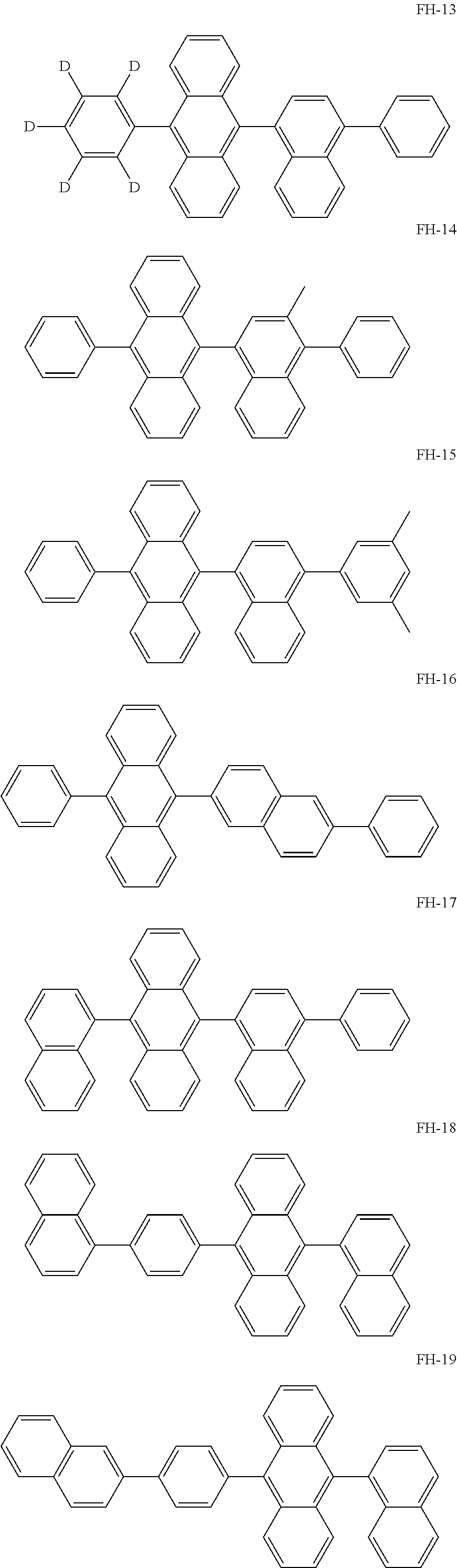


m may be the same or different.


HOMO(eV)=((HOMO(G)×27.212)−0.9899)/1.1206
LUMO(eV)=((LUMO(G)×27.212)−2.0041)/1.385
| TABLE 1 | ||||||
| Material | HOMO[eV] | HOMO − 1[eV] | LUMO[eV] | LUMO + 1[eV] | T1[eV] | S1[eV] |
| FH-18 | −5.57 | −6.08 | −2.70 | −2.31 | 1.71 | 3.17 |
| FH-19 | −5.54 | −6.11 | −2.70 | −2.37 | 1.71 | 3.15 |
| FH-21 | −5.53 | −6.07 | −2.71 | −2.31 | 1.70 | 3.12 |
| FH-29 | −5.53 | −6.11 | −2.70 | −2.30 | 1.70 | 3.12 |
| PH-8 | −5.44 | −5.86 | −2.22 | −2.17 | 2.92 | 3.12 |
| PH-12 | −5.36 | −5.75 | −2.18 | −1.99 | 3.01 | 3.20 |
| PH-13 | −5.47 | −5.90 | −2.37 | −2.16 | 2.91 | 3.13 |
| TABLE 2 | ||||
| Driving Voltage | Current Efficiency | T80 | ||
| (V) | (cd/A) | (hr@10 mA/cm2) | ||
| Example 1 | 6.2 | 5.6 | 85 |
| Example 2 | 5.9 | 50 | 170 |
| Comparative | 6.1 | 4.8 | 49 |
| Example 1 | |||
| Comparative | 6.0 | 37 | 101 |
| Example 2 | |||
Claims (19)


Applications Claiming Priority (3)
| Application Number | Priority Date | Filing Date | Title |
|---|---|---|---|
| CN201611123275 | 2016-12-08 | ||
| CN201611123275.X | 2016-12-08 | ||
| PCT/CN2017/115308 WO2018103744A1 (en) | 2016-12-08 | 2017-12-08 | Mixture, composition and organic electronic device |
Publications (2)
| Publication Number | Publication Date |
|---|---|
| US20200098992A1 US20200098992A1 (en) | 2020-03-26 |
| US10978642B2 true US10978642B2 (en) | 2021-04-13 |
Family
ID=62492240
Family Applications (1)
| Application Number | Title | Priority Date | Filing Date |
|---|---|---|---|
| US16/467,413 Active 2038-01-28 US10978642B2 (en) | 2016-12-08 | 2017-12-08 | Mixture, composition and organic electronic device |
Country Status (4)
| Country | Link |
|---|---|
| US (1) | US10978642B2 (en) |
| EP (1) | EP3553152B1 (en) |
| CN (1) | CN109790461B (en) |
| WO (1) | WO2018103744A1 (en) |
Cited By (2)
| Publication number | Priority date | Publication date | Assignee | Title |
|---|---|---|---|---|
| US11482679B2 (en) * | 2017-05-23 | 2022-10-25 | Kyushu University, National University Corporation | Compound, light-emitting lifetime lengthening agent, use of n-type compound, film and light-emitting device |
| US11515485B2 (en) * | 2018-12-05 | 2022-11-29 | Lg Display Co., Ltd. | Organic light emitting diode and organic light emitting device having the same |
Families Citing this family (8)
| Publication number | Priority date | Publication date | Assignee | Title |
|---|---|---|---|---|
| WO2018114883A1 (en) * | 2016-12-22 | 2018-06-28 | Merck Patent Gmbh | Mixtures comprising at least two organofunctional compounds |
| CN110305150B (en) * | 2019-06-29 | 2022-05-31 | 武汉天马微电子有限公司 | A thermally activated delayed fluorescent material and its application |
| CN112679413B (en) * | 2019-10-18 | 2023-02-07 | 广州华睿光电材料有限公司 | Phosphorescent host material and application thereof |
| US12545690B2 (en) | 2019-10-25 | 2026-02-10 | Universal Display Corporation | Organic electroluminescent materials and devices |
| US12522565B2 (en) | 2019-10-25 | 2026-01-13 | Universal Display Corporation | Organic electroluminescent materials and devices |
| CN114751892A (en) * | 2021-01-10 | 2022-07-15 | 浙江光昊光电科技有限公司 | Organic mixture and application thereof in organic electronic device |
| CN114763475B (en) * | 2021-01-10 | 2025-12-30 | 浙江光昊光电科技有限公司 | An organic mixture and its application in organic electronic devices |
| US12442964B2 (en) * | 2021-04-26 | 2025-10-14 | Meta Platforms Technologies, Llc | Multilayer organic solid thin films having a biaxial refractive index |
Citations (85)
| Publication number | Priority date | Publication date | Assignee | Title |
|---|---|---|---|---|
| US3567450A (en) | 1968-02-20 | 1971-03-02 | Eastman Kodak Co | Photoconductive elements containing substituted triarylamine photoconductors |
| US3615404A (en) | 1968-04-25 | 1971-10-26 | Scott Paper Co | 1 3-phenylenediamine containing photoconductive materials |
| US4720432A (en) | 1987-02-11 | 1988-01-19 | Eastman Kodak Company | Electroluminescent device with organic luminescent medium |
| US4769292A (en) | 1987-03-02 | 1988-09-06 | Eastman Kodak Company | Electroluminescent device with modified thin film luminescent zone |
| US5061569A (en) | 1990-07-26 | 1991-10-29 | Eastman Kodak Company | Electroluminescent device with organic electroluminescent medium |
| US5121029A (en) | 1987-12-11 | 1992-06-09 | Idemitsu Kosan Co., Ltd. | Electroluminescence device having an organic electroluminescent element |
| US5130603A (en) | 1989-03-20 | 1992-07-14 | Idemitsu Kosan Co., Ltd. | Organic electroluminescence device |
| US6020078A (en) | 1998-12-18 | 2000-02-01 | Eastman Kodak Company | Green organic electroluminescent devices |
| WO2000070655A2 (en) | 1999-05-13 | 2000-11-23 | The Trustees Of Princeton University | Very high efficiency organic light emitting devices based on electrophosphorescence |
| WO2001041512A1 (en) | 1999-12-01 | 2001-06-07 | The Trustees Of Princeton University | Complexes of form l2mx as phosphorescent dopants for organic leds |
| US6251531B1 (en) | 1995-02-25 | 2001-06-26 | Toyo Ink Manufacturing Co., Ltd. | Light-emitting material for organic electroluminescence device, and organic electroluminescence device for which the light-emitting material is adapted |
| US20010053462A1 (en) | 2000-05-02 | 2001-12-20 | Masayuki Mishima | Light-emitting device |
| WO2002002714A2 (en) | 2000-06-30 | 2002-01-10 | E.I. Du Pont De Nemours And Company | Electroluminescent iridium compounds with fluorinated phenylpyridines, phenylpyrimidines, and phenylquinolines and devices made with such compounds |
| WO2002015645A1 (en) | 2000-08-11 | 2002-02-21 | The Trustees Of Princeton University | Organometallic compounds and emission-shifting organic electrophosphorescence |
| US6824895B1 (en) | 2003-12-05 | 2004-11-30 | Eastman Kodak Company | Electroluminescent device containing organometallic compound with tridentate ligand |
| US6830828B2 (en) | 1998-09-14 | 2004-12-14 | The Trustees Of Princeton University | Organometallic complexes as phosphorescent emitters in organic LEDs |
| US6835469B2 (en) | 2001-10-17 | 2004-12-28 | The University Of Southern California | Phosphorescent compounds and devices comprising the same |
| CN1583691A (en) | 2004-06-04 | 2005-02-23 | 友达光电股份有限公司 | Anthracene compound and organic electroluminescent device comprising the anthracene compound |
| WO2005019373A2 (en) | 2003-08-19 | 2005-03-03 | Basf Aktiengesellschaft | Transition metal complexes comprising carbene ligands serving as emitters for organic light-emitting diodes (oled's) |
| WO2005033244A1 (en) | 2003-09-29 | 2005-04-14 | Covion Organic Semiconductors Gmbh | Metal complexes |
| US20050258742A1 (en) | 2004-05-18 | 2005-11-24 | Yui-Yi Tsai | Carbene containing metal complexes as OLEDs |
| WO2006000388A1 (en) | 2004-06-26 | 2006-01-05 | Merck Patent Gmbh | Organic electroluminescent device |
| WO2006000389A1 (en) | 2004-06-26 | 2006-01-05 | Merck Patent Gmbh | Compounds for organic electronic devices |
| EP1191613B1 (en) | 2000-09-26 | 2006-03-29 | Canon Kabushiki Kaisha | Luminescence device, display apparatus and metal coordination compound |
| US7029766B2 (en) | 2003-12-05 | 2006-04-18 | Eastman Kodak Company | Organic element for electroluminescent devices |
| WO2006058737A1 (en) | 2004-12-01 | 2006-06-08 | Merck Patent Gmbh | Compounds for organic electronic devices |
| US20060210830A1 (en) | 2005-03-15 | 2006-09-21 | Idemitsu Kosan Co., Ltd. | Aromatic amine derivative and organic electroluminescence device using the same |
| US20060222886A1 (en) | 2005-04-04 | 2006-10-05 | Raymond Kwong | Arylpyrene compounds |
| WO2006122630A1 (en) | 2005-05-20 | 2006-11-23 | Merck Patent Gmbh | Compounds for organic electronic devices |
| US20070087219A1 (en) | 2005-10-19 | 2007-04-19 | Eastman Kodak Company | Electroluminescent device |
| US20070092753A1 (en) | 2005-10-26 | 2007-04-26 | Eastman Kodak Company | Organic element for low voltage electroluminescent devices |
| WO2007065549A1 (en) | 2005-12-08 | 2007-06-14 | Merck Patent Gmbh | Organic electroluminescent devices |
| DE102005058557A1 (en) | 2005-12-08 | 2007-06-14 | Merck Patent Gmbh | Organic electroluminescent device |
| US7250532B2 (en) | 2001-03-16 | 2007-07-31 | Idemitsu Kosan Co., Ltd. | Method for producing aromatic amino compound |
| WO2007095118A2 (en) | 2006-02-10 | 2007-08-23 | Universal Display Corporation | METAL COMPLEXES OF CYCLOMETALLATED IMIDAZO[1,2-f]PHENANTHRIDINE AND DIIMIDAZO[1,2-A:1',2'-C]QUINAZOLINE LIGANDS AND ISOELECTRONIC AND BENZANNULATED ANALOGS THEREOF |
| WO2007115610A1 (en) | 2006-04-01 | 2007-10-18 | Merck Patent Gmbh | Materials for organic electroluminescent devices |
| US20070252517A1 (en) | 2006-04-27 | 2007-11-01 | Eastman Kodak Company | Electroluminescent device including an anthracene derivative |
| WO2007140847A1 (en) | 2006-06-02 | 2007-12-13 | Merck Patent Gmbh | Materials for organic electroluminescent devices |
| WO2008006449A1 (en) | 2006-07-11 | 2008-01-17 | Merck Patent Gmbh | Novel materials for organic electroluminescent devices |
| US20080027220A1 (en) | 2004-07-16 | 2008-01-31 | Merck Patent Gmbh | Metal Complexes |
| JP2008053397A (en) | 2006-08-24 | 2008-03-06 | Ricoh Co Ltd | Semiconductor device and manufacturing method thereof |
| US20080113101A1 (en) | 2006-11-09 | 2008-05-15 | Idemitsu Kosan Co., Ltd. | Organic-electroluminescence-material-containing solution, method for forming thin film of organic electroluminescence material, thin film of organic electroluminescence material and organic electroluminescence device |
| US20090053557A1 (en) * | 2007-08-23 | 2009-02-26 | Spindler Jeffrey P | Stabilized white-emitting oled device |
| US20090061681A1 (en) | 2007-09-05 | 2009-03-05 | Mcmunigal Tom | Electrical receptacle assembly |
| EP1191614B1 (en) | 2000-09-26 | 2009-05-06 | Canon Kabushiki Kaisha | Luminescence device and metal coordination compound therefor |
| US20090134784A1 (en) | 2004-10-21 | 2009-05-28 | Universal Display Corporation | Carbazole-containing materials in phosphorescent light emitting diodes |
| EP1191612B1 (en) | 2000-09-26 | 2009-09-09 | Canon Kabushiki Kaisha | Luminescence device and display apparatus |
| WO2009118087A1 (en) | 2008-03-25 | 2009-10-01 | Merck Patent Gmbh | Metal complexes |
| WO2009146770A2 (en) | 2008-06-05 | 2009-12-10 | Merck Patent Gmbh | Electronic device comprising metal complexes |
| WO2010015307A1 (en) | 2008-08-04 | 2010-02-11 | Merck Patent Gmbh | Electronic devices comprising metal complexes having isonitrile ligands |
| WO2010031485A1 (en) | 2008-09-22 | 2010-03-25 | Merck Patent Gmbh | Materials for organic electroluminescence devices |
| WO2010034125A1 (en) | 2008-09-29 | 2010-04-01 | Toronto Rehabilitation Institute | Hand hygiene compliance system |
| WO2010054731A1 (en) | 2008-11-13 | 2010-05-20 | Merck Patent Gmbh | Materials for organic electroluminescent devices |
| WO2010054728A1 (en) | 2008-11-13 | 2010-05-20 | Merck Patent Gmbh | Materials for organic electroluminescent devices |
| WO2010086089A1 (en) | 2009-02-02 | 2010-08-05 | Merck Patent Gmbh | Metal complexes |
| WO2010099852A1 (en) | 2009-03-02 | 2010-09-10 | Merck Patent Gmbh | Metal complexes having azaborol ligands and electronic device having the same |
| WO2010102709A1 (en) | 2009-03-13 | 2010-09-16 | Merck Patent Gmbh | Materials for organic electroluminescence devices |
| WO2010135519A1 (en) | 2009-05-20 | 2010-11-25 | Universal Display Corporation | Metal complexes with boron-nitrogen heterocycle containing ligands for use in organic light emitting devices |
| WO2011110277A1 (en) | 2010-03-11 | 2011-09-15 | Merck Patent Gmbh | Fibers in therapy and cosmetics |
| WO2011141110A2 (en) | 2010-05-12 | 2011-11-17 | Merck Patent Gmbh | Photo-stabilizing agents |
| WO2011157339A1 (en) | 2010-06-15 | 2011-12-22 | Merck Patent Gmbh | Metal complexes |
| WO2012007087A1 (en) | 2010-07-16 | 2012-01-19 | Merck Patent Gmbh | Metal complexes |
| WO2012007086A1 (en) | 2010-07-16 | 2012-01-19 | Merck Patent Gmbh | Metal complexes |
| WO2012007088A1 (en) | 2010-07-16 | 2012-01-19 | Merck Patent Gmbh | Metal complexes |
| US20120217869A1 (en) | 2011-02-28 | 2012-08-30 | Kyushu University National University Corporation | Delayed fluorescence material and organic electroluminescence device |
| CN102668152A (en) | 2009-12-23 | 2012-09-12 | 默克专利有限公司 | Composition including polymeric binder |
| US20120326141A1 (en) * | 2010-03-06 | 2012-12-27 | Merck Patent Gmbh | Organic electroluminescent device |
| TW201309696A (en) | 2011-07-15 | 2013-03-01 | Univ Kyushu Nat Univ Corp | Delayed fluorescent material and organic electroluminescence element using same |
| TW201309778A (en) | 2011-07-15 | 2013-03-01 | Univ Kyushu Nat Univ Corp | Organic electroluminescence element and compound used therefor |
| CN103026525A (en) | 2010-07-26 | 2013-04-03 | 默克专利有限公司 | Nanocrystals in devices |
| WO2013113349A1 (en) | 2012-01-30 | 2013-08-08 | Merck Patent Gmbh | Nanocrystals on fibers |
| WO2013133359A1 (en) | 2012-03-09 | 2013-09-12 | 国立大学法人九州大学 | Light-emitting material, and organic light-emitting element |
| WO2013154064A1 (en) | 2012-04-09 | 2013-10-17 | 国立大学法人九州大学 | Organic light emitting element, and light emitting material and compound used in same |
| TW201343874A (en) | 2012-04-25 | 2013-11-01 | Univ Kyushu Nat Univ Corp | Luminescence material and organic luminescence device |
| TW201350558A (en) | 2012-05-17 | 2013-12-16 | Univ Kyushu Nat Univ Corp | Compound, luminescence material and organic luminescence device |
| CN103483332A (en) | 2013-09-11 | 2014-01-01 | 中山大学 | Novel piezoluminescence material with thermal activation delayed fluorescence and aggregation-induced emission properties and synthetic method and application of novel piezoluminescence material |
| CN103563117A (en) | 2011-05-27 | 2014-02-05 | 环球展览公司 | Organic light-emitting devices having multi-component emissivie layer |
| WO2015180524A1 (en) | 2014-05-30 | 2015-12-03 | 广州华睿光电材料有限公司 | Organic mixture, composition containing same, organic electronic device and application |
| WO2016036171A1 (en) | 2014-09-04 | 2016-03-10 | Rohm And Haas Electronic Materials Korea Ltd. | A plurality of host materials and organic electroluminescent devices comprising the same |
| US20160093808A1 (en) | 2014-09-29 | 2016-03-31 | Universal Display Corporation | Organic electroluminescent materials and devices |
| US20170309829A1 (en) * | 2015-06-26 | 2017-10-26 | Samsung Sdi Co., Ltd. | Composition for organic optoelectronic element, organic optoelectronic element, and display device |
| US20180076393A1 (en) * | 2016-09-14 | 2018-03-15 | Universal Display Corporation | Organic electroluminescent materials and devices |
| US10454040B2 (en) * | 2012-09-18 | 2019-10-22 | Merck Patent Gmbh | Materials for electronic devices |
| US20200098996A1 (en) * | 2016-12-22 | 2020-03-26 | Merck Patent Gmbh | Mixtures comprising at least two organofunctional compounds |
| US20200176685A1 (en) * | 2018-12-04 | 2020-06-04 | Samsung Sdi Co., Ltd. | Organic optoelectronic device and display device |
Family Cites Families (4)
| Publication number | Priority date | Publication date | Assignee | Title |
|---|---|---|---|---|
| JP2686418B2 (en) | 1994-08-12 | 1997-12-08 | 東洋インキ製造株式会社 | Diarylamine derivative, production method and use thereof |
| EP2534509B1 (en) | 2010-02-10 | 2019-07-24 | 3M Innovative Properties Company | Illumination device having viscoelastic layer |
| KR101948709B1 (en) * | 2015-09-25 | 2019-02-15 | 삼성에스디아이 주식회사 | Composition for organic optoelectric device, organic optoelectric device and display device |
| KR101977163B1 (en) * | 2015-09-25 | 2019-05-10 | 삼성에스디아이 주식회사 | Composition for organic optoelectric device, organic optoelectric device and display device |
-
2017
- 2017-12-08 US US16/467,413 patent/US10978642B2/en active Active
- 2017-12-08 CN CN201780059728.3A patent/CN109790461B/en active Active
- 2017-12-08 WO PCT/CN2017/115308 patent/WO2018103744A1/en not_active Ceased
- 2017-12-08 EP EP17879321.2A patent/EP3553152B1/en active Active
Patent Citations (93)
| Publication number | Priority date | Publication date | Assignee | Title |
|---|---|---|---|---|
| US3567450A (en) | 1968-02-20 | 1971-03-02 | Eastman Kodak Co | Photoconductive elements containing substituted triarylamine photoconductors |
| US3615404A (en) | 1968-04-25 | 1971-10-26 | Scott Paper Co | 1 3-phenylenediamine containing photoconductive materials |
| US4720432A (en) | 1987-02-11 | 1988-01-19 | Eastman Kodak Company | Electroluminescent device with organic luminescent medium |
| US4769292A (en) | 1987-03-02 | 1988-09-06 | Eastman Kodak Company | Electroluminescent device with modified thin film luminescent zone |
| US5121029A (en) | 1987-12-11 | 1992-06-09 | Idemitsu Kosan Co., Ltd. | Electroluminescence device having an organic electroluminescent element |
| US5130603A (en) | 1989-03-20 | 1992-07-14 | Idemitsu Kosan Co., Ltd. | Organic electroluminescence device |
| US5061569A (en) | 1990-07-26 | 1991-10-29 | Eastman Kodak Company | Electroluminescent device with organic electroluminescent medium |
| US6251531B1 (en) | 1995-02-25 | 2001-06-26 | Toyo Ink Manufacturing Co., Ltd. | Light-emitting material for organic electroluminescence device, and organic electroluminescence device for which the light-emitting material is adapted |
| US6830828B2 (en) | 1998-09-14 | 2004-12-14 | The Trustees Of Princeton University | Organometallic complexes as phosphorescent emitters in organic LEDs |
| US6020078A (en) | 1998-12-18 | 2000-02-01 | Eastman Kodak Company | Green organic electroluminescent devices |
| WO2000070655A2 (en) | 1999-05-13 | 2000-11-23 | The Trustees Of Princeton University | Very high efficiency organic light emitting devices based on electrophosphorescence |
| WO2001041512A1 (en) | 1999-12-01 | 2001-06-07 | The Trustees Of Princeton University | Complexes of form l2mx as phosphorescent dopants for organic leds |
| US20010053462A1 (en) | 2000-05-02 | 2001-12-20 | Masayuki Mishima | Light-emitting device |
| WO2002002714A2 (en) | 2000-06-30 | 2002-01-10 | E.I. Du Pont De Nemours And Company | Electroluminescent iridium compounds with fluorinated phenylpyridines, phenylpyrimidines, and phenylquinolines and devices made with such compounds |
| WO2002015645A1 (en) | 2000-08-11 | 2002-02-21 | The Trustees Of Princeton University | Organometallic compounds and emission-shifting organic electrophosphorescence |
| EP1191614B1 (en) | 2000-09-26 | 2009-05-06 | Canon Kabushiki Kaisha | Luminescence device and metal coordination compound therefor |
| EP1191613B1 (en) | 2000-09-26 | 2006-03-29 | Canon Kabushiki Kaisha | Luminescence device, display apparatus and metal coordination compound |
| EP1191612B1 (en) | 2000-09-26 | 2009-09-09 | Canon Kabushiki Kaisha | Luminescence device and display apparatus |
| US7250532B2 (en) | 2001-03-16 | 2007-07-31 | Idemitsu Kosan Co., Ltd. | Method for producing aromatic amino compound |
| US6835469B2 (en) | 2001-10-17 | 2004-12-28 | The University Of Southern California | Phosphorescent compounds and devices comprising the same |
| WO2005019373A2 (en) | 2003-08-19 | 2005-03-03 | Basf Aktiengesellschaft | Transition metal complexes comprising carbene ligands serving as emitters for organic light-emitting diodes (oled's) |
| WO2005033244A1 (en) | 2003-09-29 | 2005-04-14 | Covion Organic Semiconductors Gmbh | Metal complexes |
| US6824895B1 (en) | 2003-12-05 | 2004-11-30 | Eastman Kodak Company | Electroluminescent device containing organometallic compound with tridentate ligand |
| US7029766B2 (en) | 2003-12-05 | 2006-04-18 | Eastman Kodak Company | Organic element for electroluminescent devices |
| US20050258742A1 (en) | 2004-05-18 | 2005-11-24 | Yui-Yi Tsai | Carbene containing metal complexes as OLEDs |
| CN1583691A (en) | 2004-06-04 | 2005-02-23 | 友达光电股份有限公司 | Anthracene compound and organic electroluminescent device comprising the anthracene compound |
| WO2006000389A1 (en) | 2004-06-26 | 2006-01-05 | Merck Patent Gmbh | Compounds for organic electronic devices |
| WO2006000388A1 (en) | 2004-06-26 | 2006-01-05 | Merck Patent Gmbh | Organic electroluminescent device |
| US20080027220A1 (en) | 2004-07-16 | 2008-01-31 | Merck Patent Gmbh | Metal Complexes |
| US20090134784A1 (en) | 2004-10-21 | 2009-05-28 | Universal Display Corporation | Carbazole-containing materials in phosphorescent light emitting diodes |
| WO2006058737A1 (en) | 2004-12-01 | 2006-06-08 | Merck Patent Gmbh | Compounds for organic electronic devices |
| US20060210830A1 (en) | 2005-03-15 | 2006-09-21 | Idemitsu Kosan Co., Ltd. | Aromatic amine derivative and organic electroluminescence device using the same |
| US20060222886A1 (en) | 2005-04-04 | 2006-10-05 | Raymond Kwong | Arylpyrene compounds |
| WO2006122630A1 (en) | 2005-05-20 | 2006-11-23 | Merck Patent Gmbh | Compounds for organic electronic devices |
| US20070087219A1 (en) | 2005-10-19 | 2007-04-19 | Eastman Kodak Company | Electroluminescent device |
| US20070092753A1 (en) | 2005-10-26 | 2007-04-26 | Eastman Kodak Company | Organic element for low voltage electroluminescent devices |
| DE102005058557A1 (en) | 2005-12-08 | 2007-06-14 | Merck Patent Gmbh | Organic electroluminescent device |
| WO2007065549A1 (en) | 2005-12-08 | 2007-06-14 | Merck Patent Gmbh | Organic electroluminescent devices |
| EP1957606A1 (en) | 2005-12-08 | 2008-08-20 | Merck Patent GmbH | Novel materials for organic electroluminiescent devices |
| US20080297037A1 (en) * | 2005-12-08 | 2008-12-04 | Merck Patent Gmbh | Organic Electroluminescent Devices |
| WO2007095118A2 (en) | 2006-02-10 | 2007-08-23 | Universal Display Corporation | METAL COMPLEXES OF CYCLOMETALLATED IMIDAZO[1,2-f]PHENANTHRIDINE AND DIIMIDAZO[1,2-A:1',2'-C]QUINAZOLINE LIGANDS AND ISOELECTRONIC AND BENZANNULATED ANALOGS THEREOF |
| WO2007115610A1 (en) | 2006-04-01 | 2007-10-18 | Merck Patent Gmbh | Materials for organic electroluminescent devices |
| US20070252517A1 (en) | 2006-04-27 | 2007-11-01 | Eastman Kodak Company | Electroluminescent device including an anthracene derivative |
| WO2007140847A1 (en) | 2006-06-02 | 2007-12-13 | Merck Patent Gmbh | Materials for organic electroluminescent devices |
| WO2008006449A1 (en) | 2006-07-11 | 2008-01-17 | Merck Patent Gmbh | Novel materials for organic electroluminescent devices |
| CN101490207A (en) | 2006-07-11 | 2009-07-22 | 默克专利有限公司 | Novel materials for organic electroluminescent devices |
| JP2008053397A (en) | 2006-08-24 | 2008-03-06 | Ricoh Co Ltd | Semiconductor device and manufacturing method thereof |
| US20080113101A1 (en) | 2006-11-09 | 2008-05-15 | Idemitsu Kosan Co., Ltd. | Organic-electroluminescence-material-containing solution, method for forming thin film of organic electroluminescence material, thin film of organic electroluminescence material and organic electroluminescence device |
| US20090053557A1 (en) * | 2007-08-23 | 2009-02-26 | Spindler Jeffrey P | Stabilized white-emitting oled device |
| US20090061681A1 (en) | 2007-09-05 | 2009-03-05 | Mcmunigal Tom | Electrical receptacle assembly |
| WO2009118087A1 (en) | 2008-03-25 | 2009-10-01 | Merck Patent Gmbh | Metal complexes |
| WO2009146770A2 (en) | 2008-06-05 | 2009-12-10 | Merck Patent Gmbh | Electronic device comprising metal complexes |
| WO2010015307A1 (en) | 2008-08-04 | 2010-02-11 | Merck Patent Gmbh | Electronic devices comprising metal complexes having isonitrile ligands |
| WO2010031485A1 (en) | 2008-09-22 | 2010-03-25 | Merck Patent Gmbh | Materials for organic electroluminescence devices |
| WO2010034125A1 (en) | 2008-09-29 | 2010-04-01 | Toronto Rehabilitation Institute | Hand hygiene compliance system |
| WO2010054731A1 (en) | 2008-11-13 | 2010-05-20 | Merck Patent Gmbh | Materials for organic electroluminescent devices |
| WO2010054728A1 (en) | 2008-11-13 | 2010-05-20 | Merck Patent Gmbh | Materials for organic electroluminescent devices |
| WO2010086089A1 (en) | 2009-02-02 | 2010-08-05 | Merck Patent Gmbh | Metal complexes |
| CN102282150A (en) | 2009-02-02 | 2011-12-14 | 默克专利有限公司 | Metal complexes |
| WO2010099852A1 (en) | 2009-03-02 | 2010-09-10 | Merck Patent Gmbh | Metal complexes having azaborol ligands and electronic device having the same |
| US20120004407A1 (en) | 2009-03-02 | 2012-01-05 | Merck Patent Gmbh | Metal complexes having azaborol ligands and electronic device having the same |
| WO2010102709A1 (en) | 2009-03-13 | 2010-09-16 | Merck Patent Gmbh | Materials for organic electroluminescence devices |
| WO2010135519A1 (en) | 2009-05-20 | 2010-11-25 | Universal Display Corporation | Metal complexes with boron-nitrogen heterocycle containing ligands for use in organic light emitting devices |
| CN102668152A (en) | 2009-12-23 | 2012-09-12 | 默克专利有限公司 | Composition including polymeric binder |
| US20120326141A1 (en) * | 2010-03-06 | 2012-12-27 | Merck Patent Gmbh | Organic electroluminescent device |
| WO2011110277A1 (en) | 2010-03-11 | 2011-09-15 | Merck Patent Gmbh | Fibers in therapy and cosmetics |
| WO2011141110A2 (en) | 2010-05-12 | 2011-11-17 | Merck Patent Gmbh | Photo-stabilizing agents |
| WO2011157339A1 (en) | 2010-06-15 | 2011-12-22 | Merck Patent Gmbh | Metal complexes |
| WO2012007086A1 (en) | 2010-07-16 | 2012-01-19 | Merck Patent Gmbh | Metal complexes |
| WO2012007088A1 (en) | 2010-07-16 | 2012-01-19 | Merck Patent Gmbh | Metal complexes |
| WO2012007087A1 (en) | 2010-07-16 | 2012-01-19 | Merck Patent Gmbh | Metal complexes |
| CN103026525A (en) | 2010-07-26 | 2013-04-03 | 默克专利有限公司 | Nanocrystals in devices |
| US20120217869A1 (en) | 2011-02-28 | 2012-08-30 | Kyushu University National University Corporation | Delayed fluorescence material and organic electroluminescence device |
| CN103563117A (en) | 2011-05-27 | 2014-02-05 | 环球展览公司 | Organic light-emitting devices having multi-component emissivie layer |
| US20140197389A1 (en) * | 2011-05-27 | 2014-07-17 | Universal Display Corporation | Oled having multi-component emissive layer |
| TW201309696A (en) | 2011-07-15 | 2013-03-01 | Univ Kyushu Nat Univ Corp | Delayed fluorescent material and organic electroluminescence element using same |
| TW201309778A (en) | 2011-07-15 | 2013-03-01 | Univ Kyushu Nat Univ Corp | Organic electroluminescence element and compound used therefor |
| WO2013113349A1 (en) | 2012-01-30 | 2013-08-08 | Merck Patent Gmbh | Nanocrystals on fibers |
| CN104081553A (en) | 2012-01-30 | 2014-10-01 | 默克专利有限公司 | Nanocrystals on fibers |
| WO2013133359A1 (en) | 2012-03-09 | 2013-09-12 | 国立大学法人九州大学 | Light-emitting material, and organic light-emitting element |
| WO2013154064A1 (en) | 2012-04-09 | 2013-10-17 | 国立大学法人九州大学 | Organic light emitting element, and light emitting material and compound used in same |
| TW201343874A (en) | 2012-04-25 | 2013-11-01 | Univ Kyushu Nat Univ Corp | Luminescence material and organic luminescence device |
| TW201350558A (en) | 2012-05-17 | 2013-12-16 | Univ Kyushu Nat Univ Corp | Compound, luminescence material and organic luminescence device |
| US10454040B2 (en) * | 2012-09-18 | 2019-10-22 | Merck Patent Gmbh | Materials for electronic devices |
| CN103483332A (en) | 2013-09-11 | 2014-01-01 | 中山大学 | Novel piezoluminescence material with thermal activation delayed fluorescence and aggregation-induced emission properties and synthetic method and application of novel piezoluminescence material |
| WO2015180524A1 (en) | 2014-05-30 | 2015-12-03 | 广州华睿光电材料有限公司 | Organic mixture, composition containing same, organic electronic device and application |
| US20170194585A1 (en) * | 2014-05-30 | 2017-07-06 | Guangzhou Chinaray Optoelectronic Materials Ltd. | Organic mixture, formulation and organic electronic device comprising thereof, and their applications |
| WO2016036171A1 (en) | 2014-09-04 | 2016-03-10 | Rohm And Haas Electronic Materials Korea Ltd. | A plurality of host materials and organic electroluminescent devices comprising the same |
| US20160093808A1 (en) | 2014-09-29 | 2016-03-31 | Universal Display Corporation | Organic electroluminescent materials and devices |
| US20170309829A1 (en) * | 2015-06-26 | 2017-10-26 | Samsung Sdi Co., Ltd. | Composition for organic optoelectronic element, organic optoelectronic element, and display device |
| US20180076393A1 (en) * | 2016-09-14 | 2018-03-15 | Universal Display Corporation | Organic electroluminescent materials and devices |
| US20200098996A1 (en) * | 2016-12-22 | 2020-03-26 | Merck Patent Gmbh | Mixtures comprising at least two organofunctional compounds |
| US20200176685A1 (en) * | 2018-12-04 | 2020-06-04 | Samsung Sdi Co., Ltd. | Organic optoelectronic device and display device |
Non-Patent Citations (30)
Cited By (2)
| Publication number | Priority date | Publication date | Assignee | Title |
|---|---|---|---|---|
| US11482679B2 (en) * | 2017-05-23 | 2022-10-25 | Kyushu University, National University Corporation | Compound, light-emitting lifetime lengthening agent, use of n-type compound, film and light-emitting device |
| US11515485B2 (en) * | 2018-12-05 | 2022-11-29 | Lg Display Co., Ltd. | Organic light emitting diode and organic light emitting device having the same |
Also Published As
| Publication number | Publication date |
|---|---|
| EP3553152B1 (en) | 2021-02-17 |
| US20200098992A1 (en) | 2020-03-26 |
| WO2018103744A1 (en) | 2018-06-14 |
| CN109790461B (en) | 2022-08-12 |
| CN109790461A (en) | 2019-05-21 |
| EP3553152A1 (en) | 2019-10-16 |
| EP3553152A4 (en) | 2019-12-18 |
Similar Documents
| Publication | Publication Date | Title |
|---|---|---|
| US10978642B2 (en) | Mixture, composition and organic electronic device | |
| CN109803957B (en) | Triazine Fused Ring Derivatives and Their Applications in Organic Electronic Devices | |
| CN110845501B (en) | Arylamine compound and application thereof in organic electronic device | |
| US10323180B2 (en) | Deuterated organic compound, mixture and composition containing said compound, and organic electronic device | |
| US20190319197A1 (en) | Organic compound, applications thereof, organic mixture, and organic electronic device | |
| US20190378982A1 (en) | Organic mixture, composition, organic electronic device and application | |
| CN110759835B (en) | Perylenequinone organic compound and application thereof | |
| CN110818642B (en) | Heterocyclic arylamine compound and application thereof in organic electronic device | |
| CN107004778B (en) | Organic mixture, composition containing organic mixture, organic electronic device and application | |
| US20170365789A1 (en) | Compound, mixture comprising the same, composition and organic electronic device | |
| US11292875B2 (en) | Cross-linkable polymer based on Diels-Alder reaction and use thereof in organic electronic device | |
| US11594690B2 (en) | Organometallic complex, and polymer, mixture and formulation comprising same, and use thereof in electronic device | |
| US20190378991A1 (en) | Organic mixture, composition, and organic electronic component | |
| US11453745B2 (en) | High polymer, mixture containing same, composition, organic electronic component, and monomer for polymerization | |
| CN110760164B (en) | Organic mixture, composition containing organic mixture, organic electronic device and application | |
| CN111278892B (en) | Polymers, mixtures, compositions containing amide bond groups and uses thereof | |
| US20200185615A1 (en) | Organic chemical compound, organic mixture, and organic electronic component | |
| CN116783159A (en) | Organic compounds and their applications in organic electronic devices | |
| US11404644B2 (en) | Organic functional compounds, mixtures, formulations, organic functional thin films and preparation methods therefor and organic electronic devices | |
| US11672174B2 (en) | Pyrene-triazine derivative and applications thereof in organic electronic component | |
| US11161933B2 (en) | Conjugated polymer and use thereof in organic electronic device | |
| US20200109235A1 (en) | Conjugated polymer and use thereof in organic electronic device | |
| CN105226193B (en) | Electroluminescent device containing fused ring compound and metal organic complex | |
| WO2018099431A1 (en) | Pyrene organic compound, preparation method therefor and application thereof | |
| US20240343715A1 (en) | Organic compounds, mixtures and formulations comprising same, organic electronic devices, and applications of compounds |
Legal Events
| Date | Code | Title | Description |
|---|---|---|---|
| FEPP | Fee payment procedure |
Free format text: ENTITY STATUS SET TO UNDISCOUNTED (ORIGINAL EVENT CODE: BIG.); ENTITY STATUS OF PATENT OWNER: LARGE ENTITY |
|
| AS | Assignment |
Owner name: GUANGZHOU CHINARAY OPTOELECTRONIC MATERIALS LTD., CHINA Free format text: ASSIGNMENT OF ASSIGNORS INTEREST;ASSIGNORS:PAN, JUNYOU;TAN, JIAHUI;SIGNING DATES FROM 20190603 TO 20190604;REEL/FRAME:049417/0434 |
|
| STPP | Information on status: patent application and granting procedure in general |
Free format text: RESPONSE TO NON-FINAL OFFICE ACTION ENTERED AND FORWARDED TO EXAMINER |
|
| STPP | Information on status: patent application and granting procedure in general |
Free format text: PUBLICATIONS -- ISSUE FEE PAYMENT VERIFIED |
|
| STCF | Information on status: patent grant |
Free format text: PATENTED CASE |
|
| MAFP | Maintenance fee payment |
Free format text: PAYMENT OF MAINTENANCE FEE, 4TH YEAR, LARGE ENTITY (ORIGINAL EVENT CODE: M1551); ENTITY STATUS OF PATENT OWNER: LARGE ENTITY Year of fee payment: 4 |