US10965212B2 - Switched-mode power supply with bypass mode - Google Patents
Switched-mode power supply with bypass mode Download PDFInfo
- Publication number
- US10965212B2 US10965212B2 US16/385,214 US201916385214A US10965212B2 US 10965212 B2 US10965212 B2 US 10965212B2 US 201916385214 A US201916385214 A US 201916385214A US 10965212 B2 US10965212 B2 US 10965212B2
- Authority
- US
- United States
- Prior art keywords
- coupled
- output
- transistor
- power supply
- input
- Prior art date
- Legal status (The legal status is an assumption and is not a legal conclusion. Google has not performed a legal analysis and makes no representation as to the accuracy of the status listed.)
- Active
Links
- 230000000737 periodic effect Effects 0.000 claims description 8
- 239000003990 capacitor Substances 0.000 description 4
- 230000004048 modification Effects 0.000 description 4
- 238000012986 modification Methods 0.000 description 4
- 238000000034 method Methods 0.000 description 3
- 230000004075 alteration Effects 0.000 description 2
- 230000008901 benefit Effects 0.000 description 2
- 230000007423 decrease Effects 0.000 description 2
- 230000006872 improvement Effects 0.000 description 2
- 230000000750 progressive effect Effects 0.000 description 2
- 230000008859 change Effects 0.000 description 1
- 230000000630 rising effect Effects 0.000 description 1
- 239000004065 semiconductor Substances 0.000 description 1
- 230000007704 transition Effects 0.000 description 1
Images


Classifications
-
- H—ELECTRICITY
- H02—GENERATION; CONVERSION OR DISTRIBUTION OF ELECTRIC POWER
- H02M—APPARATUS FOR CONVERSION BETWEEN AC AND AC, BETWEEN AC AND DC, OR BETWEEN DC AND DC, AND FOR USE WITH MAINS OR SIMILAR POWER SUPPLY SYSTEMS; CONVERSION OF DC OR AC INPUT POWER INTO SURGE OUTPUT POWER; CONTROL OR REGULATION THEREOF
- H02M3/00—Conversion of DC power input into DC power output
- H02M3/02—Conversion of DC power input into DC power output without intermediate conversion into AC
- H02M3/04—Conversion of DC power input into DC power output without intermediate conversion into AC by static converters
- H02M3/10—Conversion of DC power input into DC power output without intermediate conversion into AC by static converters using discharge tubes with control electrode or semiconductor devices with control electrode
- H02M3/145—Conversion of DC power input into DC power output without intermediate conversion into AC by static converters using discharge tubes with control electrode or semiconductor devices with control electrode using devices of a triode or transistor type requiring continuous application of a control signal
- H02M3/155—Conversion of DC power input into DC power output without intermediate conversion into AC by static converters using discharge tubes with control electrode or semiconductor devices with control electrode using devices of a triode or transistor type requiring continuous application of a control signal using semiconductor devices only
- H02M3/156—Conversion of DC power input into DC power output without intermediate conversion into AC by static converters using discharge tubes with control electrode or semiconductor devices with control electrode using devices of a triode or transistor type requiring continuous application of a control signal using semiconductor devices only with automatic control of output voltage or current, e.g. switching regulators
- H02M3/158—Conversion of DC power input into DC power output without intermediate conversion into AC by static converters using discharge tubes with control electrode or semiconductor devices with control electrode using devices of a triode or transistor type requiring continuous application of a control signal using semiconductor devices only with automatic control of output voltage or current, e.g. switching regulators including plural semiconductor devices as final control devices for a single load
-
- H—ELECTRICITY
- H02—GENERATION; CONVERSION OR DISTRIBUTION OF ELECTRIC POWER
- H02M—APPARATUS FOR CONVERSION BETWEEN AC AND AC, BETWEEN AC AND DC, OR BETWEEN DC AND DC, AND FOR USE WITH MAINS OR SIMILAR POWER SUPPLY SYSTEMS; CONVERSION OF DC OR AC INPUT POWER INTO SURGE OUTPUT POWER; CONTROL OR REGULATION THEREOF
- H02M1/00—Details of apparatus for conversion
- H02M1/0003—Details of control, feedback or regulation circuits
- H02M1/0025—Arrangements for modifying reference values, feedback values or error values in the control loop of a converter
-
- H—ELECTRICITY
- H02—GENERATION; CONVERSION OR DISTRIBUTION OF ELECTRIC POWER
- H02M—APPARATUS FOR CONVERSION BETWEEN AC AND AC, BETWEEN AC AND DC, OR BETWEEN DC AND DC, AND FOR USE WITH MAINS OR SIMILAR POWER SUPPLY SYSTEMS; CONVERSION OF DC OR AC INPUT POWER INTO SURGE OUTPUT POWER; CONTROL OR REGULATION THEREOF
- H02M1/00—Details of apparatus for conversion
- H02M1/0003—Details of control, feedback or regulation circuits
- H02M1/0032—Control circuits allowing low power mode operation, e.g. in standby mode
-
- H—ELECTRICITY
- H02—GENERATION; CONVERSION OR DISTRIBUTION OF ELECTRIC POWER
- H02M—APPARATUS FOR CONVERSION BETWEEN AC AND AC, BETWEEN AC AND DC, OR BETWEEN DC AND DC, AND FOR USE WITH MAINS OR SIMILAR POWER SUPPLY SYSTEMS; CONVERSION OF DC OR AC INPUT POWER INTO SURGE OUTPUT POWER; CONTROL OR REGULATION THEREOF
- H02M1/00—Details of apparatus for conversion
- H02M1/32—Means for protecting converters other than automatic disconnection
-
- H—ELECTRICITY
- H02—GENERATION; CONVERSION OR DISTRIBUTION OF ELECTRIC POWER
- H02M—APPARATUS FOR CONVERSION BETWEEN AC AND AC, BETWEEN AC AND DC, OR BETWEEN DC AND DC, AND FOR USE WITH MAINS OR SIMILAR POWER SUPPLY SYSTEMS; CONVERSION OF DC OR AC INPUT POWER INTO SURGE OUTPUT POWER; CONTROL OR REGULATION THEREOF
- H02M3/00—Conversion of DC power input into DC power output
- H02M3/02—Conversion of DC power input into DC power output without intermediate conversion into AC
- H02M3/04—Conversion of DC power input into DC power output without intermediate conversion into AC by static converters
- H02M3/10—Conversion of DC power input into DC power output without intermediate conversion into AC by static converters using discharge tubes with control electrode or semiconductor devices with control electrode
- H02M3/145—Conversion of DC power input into DC power output without intermediate conversion into AC by static converters using discharge tubes with control electrode or semiconductor devices with control electrode using devices of a triode or transistor type requiring continuous application of a control signal
- H02M3/155—Conversion of DC power input into DC power output without intermediate conversion into AC by static converters using discharge tubes with control electrode or semiconductor devices with control electrode using devices of a triode or transistor type requiring continuous application of a control signal using semiconductor devices only
- H02M3/156—Conversion of DC power input into DC power output without intermediate conversion into AC by static converters using discharge tubes with control electrode or semiconductor devices with control electrode using devices of a triode or transistor type requiring continuous application of a control signal using semiconductor devices only with automatic control of output voltage or current, e.g. switching regulators
-
- Y—GENERAL TAGGING OF NEW TECHNOLOGICAL DEVELOPMENTS; GENERAL TAGGING OF CROSS-SECTIONAL TECHNOLOGIES SPANNING OVER SEVERAL SECTIONS OF THE IPC; TECHNICAL SUBJECTS COVERED BY FORMER USPC CROSS-REFERENCE ART COLLECTIONS [XRACs] AND DIGESTS
- Y02—TECHNOLOGIES OR APPLICATIONS FOR MITIGATION OR ADAPTATION AGAINST CLIMATE CHANGE
- Y02B—CLIMATE CHANGE MITIGATION TECHNOLOGIES RELATED TO BUILDINGS, e.g. HOUSING, HOUSE APPLIANCES OR RELATED END-USER APPLICATIONS
- Y02B70/00—Technologies for an efficient end-user side electric power management and consumption
- Y02B70/10—Technologies improving the efficiency by using switched-mode power supplies [SMPS], i.e. efficient power electronics conversion e.g. power factor correction or reduction of losses in power supplies or efficient standby modes
Definitions
- the present disclosure concerns generally to an electronic system and method, and, in particular embodiments, to switched-mode power supplies.
- Switched-mode power supplies are DC/DC converters which incorporate one or more switching elements. Like other types of power supplies, switched-mode power supplied transfer a power supplied by a source DC to a load, and doing so, modify one of the current or voltage characteristics.
- Some embodiments relate to switched-mode power supplies and their operating modes.
- An embodiment provides a switched-mode power supply wherein the reference voltage of the feedback loop has an adjustable value.
- the power supply is a buck converter, the reference voltage being capable of taking a value greater than or equal to the value of the power supply voltage divided by the closed loop gain of the system.
- the power supply is a boost converter, the reference voltage being capable of taking a value smaller than or equal to the value of the power supply voltage divided by the closed loop gain of the system.
- the power supply comprises first and second series-connected transistors, the first transistor being connected between the ground and a first node and the second transistor being connected between the first node and a node of application of the power supply voltage, the first and second transistors being capable of being controlled by a circuit for generating the control signals of the first and second transistors.
- the power supply comprises a first circuit capable of detecting whether the duty cycle of an input signal of the generation circuit is substantially equal to 100%.
- the power supply comprises a second circuit capable of maintaining the second transistor on if the duty cycle of the input signal of the generation circuit is substantially equal to 100%.
- the second circuit comprises an AND gate.
- the first circuit comprises a counter having its reset input connected to the input signal of the generation circuit.
- the feedback loop is located between the output node of the power supply and a second node.
- the second node is coupled to ground by a first resistor, the second node being coupled to the output node by a second resistor.
- the reference voltage is supplied by a third circuit comprising a resistive feedback loop having an adjustable resistance.
- the reference voltage is supplied by a third circuit comprising a resistive feedback loop having its output coupled to the output of the circuit by a resistive block having an adjustable resistance.
- An embodiment provides a method of using a power supply comprising switching from a first state of the reference voltage of the feedback loop to a second state.
- the power supply is a buck converter
- the reference voltage in the second state is greater than or equal to the power supply voltage divided by the closed loop gain of the system.
- the power supply is a boost converter
- the reference voltage in the second state is smaller than or equal to a power supply voltage divided by the closed loop gain of the system.
- the method comprises: determining, by using a first circuit, whether the duty cycle of an input signal of the circuit for generating the control signals of two transistors is substantially equal to 100%; and turning off the components of the power supply other than a second circuit ensuring the connection between the power supply output and a node of application of the power supply voltage.
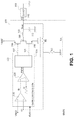
- FIG. 1 is a simplified representation of an example of a switched-mode power supply
- FIG. 2 is a simplified representation of an embodiment of a switched-mode power supply
- FIG. 3 illustrates an operating mode of the switched-mode power supply of FIG. 2 ;
- FIG. 4 is a simplified representation of an embodiment of a switched-mode power supply
- FIGS. 5, 6, and 7 partially show variations of the embodiment of FIG. 2 ;
- FIGS. 8 and 9 partially show variations of the embodiment of FIG. 4 ;
- FIG. 10 is a simplified representation of another embodiment of a switched-mode power supply.
- FIG. 1 is a simplified representation of an example of switched-mode power supply 100 (SMPS) receiving as an input a power supply voltage VBAT and a reference voltage VREF and supplying a voltage Vout to an output node 102 (V 2 ).
- the power supply of FIG. 1 is a buck converter, that is, voltage Vout is smaller than power supply voltage VBAT.
- Output node 102 is coupled to ground by a load 103 (LOAD).
- Load 103 is thus powered by converter 100 .
- Converter 100 comprises two switches 104 and 106 series connected between the node of application of power supply voltage VBAT and the ground.
- switch 104 is an N-channel metal-oxide-semiconductor (MOS) transistor and switch 106 is a P-channel MOS transistor.
- MOS metal-oxide-semiconductor
- the source of transistor 106 is connected to a node 108 and its drain is connected to the node of application of voltage VBAT.
- the source of transistor 104 is connected to ground and its drain is connected to node 108 .
- An inductance no is connected between nodes 108 and 102 .
- Node 102 is further coupled to ground by a capacitor 112 .
- Transistors 104 and 106 are controlled by a control circuit 114 (SMPS CONTROLLER). More particularly, transistor 106 is controlled by an output 107 of control circuit 114 , and transistor 104 is controlled by an output 105 of control circuit 114 .
- Control circuit 114 comprises a comparator 116 , for example, an error amplifier. The inputs of comparator 116 are connected to a node of application of reference voltage VREF and to a node V 1 . The output of comparator 116 supplies a signal Er, representative of the voltage difference between reference voltage VREF and the voltage of node V 1 .
- Node V 1 is coupled to output node 102 by a resistive block RA.
- Power supply 100 thus comprises a resistive feedback loop between output node 102 and node V 1 .
- “Feedback voltage” designates the voltage of node V 1 , that is, the input voltage of the control circuit depending on output voltage Vout.
- Block RA comprises for example two resistors, a resistor R 1 connected between nodes 102 and V 1 and a resistor R 2 connected between node V 1 and the ground.
- Control circuit 114 further comprises a comparator 120 receiving as an input signal Er and a periodic sawtooth signal D. Comparator 120 outputs a pulse-width modulated signal PWM.
- Signal PWM is a periodic binary signal comprising a high state and a low state. The duty cycle of signal PWM is controlled by signal Er.
- the larger the difference between reference voltage VREF and the feedback voltage, that is, signal Er the larger the duty cycle of signal PWM.
- Control circuit 114 further comprises driver 122 for generating the control signals of transistors 104 and 106 . More particularly, when signal PWM is in the high state, driver 122 turns on switch 106 and turns off switch 104 and when signal PWM is in the low state, driver 122 turns off switch 106 and turns on switch 104 .
- the use of a switched-mode power supply such as power supply 100 may be neither cost-effective nor efficient.
- bypass mode It may then be desired for output node 102 of the switched-mode power supply to directly and continuously receive the power supplied by the power source.
- Such an operating mode is called bypass mode. It could be envisaged to simply connect, for example, by using a switch, the source of application of voltage VBAT to node 102 . However, the turning on of this switch may cause a current peak on node 102 . Such a current peak may risk damaging certain elements of power supply 100 , for example, switches connecting two nodes or a power source and a node.
- FIG. 2 is a simplified representation of an embodiment of a switched-mode power supply 200 powering load 103 and receiving power supply voltage VBAT.
- Power supply 200 is, like power supply 100 of FIG. 1 , a buck converter.
- Power supply 200 comprises the elements of power supply 100 .
- power supply 200 comprises control circuit 114 , switches 104 and 106 , inductance 110 , and capacitor 112 .
- the feedback loop is a resistive feedback loop having an adjustable value. More particularly, the feedback loop comprises a resistive block 202 (R), different from resistive block RA of power supply 100 , having at least two resistive states. Like block RA, block R is connected between nodes V 1 and V 2 and comprises resistor R 1 connected between nodes V 1 and V 2 . Node V 1 is further coupled to ground by resistor R 2 in series with a switch 204 . Switch 204 is controlled by a binary signal F. Node V 1 is also coupled to ground by a resistor RH in series with another switch 206 . Switch 206 is controlled by a binary signal F corresponding to the signal inverse to signal F. Switches 204 and 206 are for example MOS transistors.
- Power supply 200 further comprises an AND gate 208 having its inputs connected to output 107 of control circuit 114 and to a node of application of a voltage FB.
- the output signal of gate 208 controls transistor 106 .
- the AND gate may optionally be replaced with a circuit capable of maintaining, on order, transistor 106 on.
- Power supply 200 further comprises a circuit 210 comprising a counter 212 (COUNTER N).
- Counter 212 outputs a signal RFB and is incremented, for example, at each rising edge of a clock signal CLK.
- Clock signal CLK corresponds to the clock signal of control circuit 114 and, in particular, clock signal CLK has the same frequency as input signal D of comparator 120 .
- Reset input R of counter 212 is coupled to the output of comparator 120 and thus receives signal PWM or a signal representative of signal PWM.
- input R is coupled to the output of comparator 120 by an inverter. However, there may be no such inverter. The counter is thus reset each time signal PWM takes the low value.
- FIG. 3 illustrates, in the form of blocks, an operating mode of switched-mode power supply 200 of FIG. 2 .
- the described operating mode corresponds to the passing from a state 300 (SMPS) where load 103 is powered by switched-mode power supply 200 , to a state 320 (BYPASS) in bypass mode, where load 103 is directly powered by the source of application of voltage VBAT, through switch 106 of the converter.
- SMPS state 300
- BYPASS state 320
- the operating mode comprises a step 302 (MODIFY RESISTANCE) during which the resistance of resistive block R is modified, for example, to switch from a first state to a second state.
- the characteristics of the first state are selected so that voltage Vout is smaller than voltage VBAT and the characteristics of the second state are selected so that voltage Vout is equal to voltage VBAT (saturation).
- V out V REF*(1 +R 1 /R 2).
- Reference voltage VREF as well as resistors R 1 and R 2 , are selected so that voltage Vout is smaller than voltage VBAT.
- V out V REF*(1 +R 1 /RH ).
- Resistor RH may be selected to have: V REF*(1 +R 1 /RH ) ⁇ V BAT.
- resistor RH is, in this example, smaller than the value of resistor R 2 .
- the resistor is modified so that the quotient of the resistance between nodes V 1 and V 2 to the resistance between node V 1 and the ground increases.
- Such a state switching of resistive block R causes a progressive increase of voltage V 1 .
- Voltage V 1 then increases to be greater than or equal to power supply voltage VBAT.
- Such an increase comprises no current peak risking damaging components.
- the state switching of resistor block R causes a variation of the duty cycle of signal PWM. More particularly, the more voltage V 1 increases, the more the duty cycle of signal PWM increases, to reach 100% when voltage Vout becomes equal to voltage VBAT.
- counter 212 is reset by signal PWM once per period of clock signal CLK.
- output signal RFB of counter 212 causes the application of voltage FB to an input of gate 208 .
- control circuit 114 and circuit 210 are turned off, and, e.g., the outputs of driver 122 stop switching. This corresponds to step 312 (SWITCH OFF SMPS).
- bypass mode 320 that is, load 103 is directly powered by the node of application of voltage VBAT, that is, constantly via switch 106 , transistor 106 being kept on by voltage FB.
- An advantage of this embodiment is that the increase of voltage Vout has been progressive, in the same way as the increase of voltage V 1 caused by the modification of the resistance of the feedback loop.
- FIG. 4 is a simplified representation of an embodiment of a switched-mode power supply 400 powering load 103 .
- Power supply 400 is a buck converter and comprises elements similar to power supply 200 .
- power supply 400 comprises control circuit 114 , gate 208 , transistors 106 and 104 , inductance 110 , capacitor 112 , and circuit 210 .
- Nodes V 1 and V 2 are coupled by a resistive block 402 .
- Resistive block 402 for example has a fixed resistance value.
- Block 402 is for example similar to resistive block RA of FIG. 1 .
- Power supply 400 further comprises a circuit 404 enabling to modify reference voltage VREF.
- Circuit 404 for example comprises an amplifier circuit having an adjustable gain.
- Another example of circuit 404 comprises a voltage dividing bridge. Two examples of circuit 404 are illustrated in FIGS. 8 and 9 .
- the operating mode of power supply 400 is similar to that described in relation with FIG. 3 , except for step 302 which is replaced with a step during which reference voltage VREF becomes greater than or equal to the power supply voltage divided by the closed loop gain of the system. The other steps remain identical.
- FIG. 5 shows a variation of a portion of the embodiment of FIG. 2 . More particularly, FIG. 5 shows another example of a resistive block R, located between nodes V 1 and V 2 .
- Nodes V 1 and V 2 are, as in the example of FIG. 2 , coupled by a resistor R 3 , for example, having a resistance equal to that of resistor R 1 .
- Node V 1 is, further, coupled to ground by two series-connected resistors R 4 and R 5 .
- Resistor R 5 is connected to ground and resistor R 4 is connected to node V 1 .
- the value of resistance R 4 is for example equal to the value of resistance RH of FIG. 2
- resistor R 5 is for example selected so that the sum of the values of resistances R 4 and R 5 are equal to the value of resistance R 2 .
- Connection node 402 of resistors R 4 and R 5 is further coupled to ground by a switch 405 , for example, a MOS transistor.
- the first state of resistive block R corresponds to a state where switch 405 is off. Node V 1 is thus coupled to ground by a resistor equivalent to R 2 .
- the second state of resistive block R corresponds to a state where switch 405 is on. Node V 1 is thus coupled to ground by resistor R 4 .
- FIG. 6 shows another variation of a portion of the embodiment of FIG. 2 . More particularly, FIG. 6 shows another example of a resistive block R, located between nodes V 1 and V 2 .
- a resistor R 6 for example, having a resistance equal to that of resistor R 1 , is connected between node V 2 and a node 502 .
- a switch 504 and a resistor R 7 are connected in parallel between node 502 and node V 1 .
- node V 1 is coupled to ground by resistor R 8 , for example, having a resistance equal to that of resistor R 2 .
- the first state of resistive block R corresponds to the state where switch 504 is on.
- the resistance between node V 1 and node V 2 is R 6 , as in the first state of block R of FIG. 2 .
- the second state of resistive block R corresponds to the state where switch 504 is off.
- the resistance between nodes V 1 and V 2 is R 6 +R 7 and is thus greater than the resistance between node V 1 and node V 2 of the first state.
- FIG. 7 shows another variation of a portion of the embodiment of FIG. 2 . More particularly, FIG. 7 shows another example of a resistive block R, located between nodes V 1 and V 2 .
- Nodes V 1 and V 2 are connected by a switch 602 , for example, a transistor, in series with a resistor R 9 , for example, having a resistance equal to that of resistor R 1 .
- Nodes V 1 and V 2 are also connected by a switch 604 , for example, a transistor, in series with a resistor R 10 .
- Switch 602 and resistor R 9 are thus in parallel with switch 604 and resistor R 10 .
- Node V 1 is also coupled to ground by resistor R 11 , for example, having a resistance equal to that of resistor R 2 .
- the first state of resistive block R corresponds to the state where switch 602 is on and switch 604 is off. Thus, the resistance between node V 1 and node V 2 is R 9 .
- the second state of resistive block R corresponds to the state when switch 602 is off and switch 604 is on.
- the resistance between node V 1 and node V 2 is R 10 .
- FIGS. 8 and 9 partially show variations of the embodiment of FIG. 4 . More particularly, FIGS. 8 and 9 show examples of circuits 404 .
- the circuits 404 of FIGS. 8 and 9 receive as an input a voltage VREFin, for example substantially constant, and output reference voltage VREF.
- circuit 404 comprises an operational amplifier 406 receiving at its positive input (+) voltage VREFin and outputting voltage VREF.
- the negative input ( ⁇ ) of operational amplifier 406 is coupled to its output by a resistive block 408 (R′) having an adjustable resistance.
- Block 408 for example has a structure similar to a resistive block R such as described in relation with FIG. 2, 5, 6 , or 7 .
- circuit 404 similarly comprises operational amplifier 406 receiving at its positive input (+) voltage VREFin.
- the negative input ( ⁇ ) of operational amplifier 406 is coupled to its output by a resistor Rf 1 , the negative input of operational amplifier 406 being coupled to ground by a resistor Rf 2 .
- the output of the operational amplifier is also coupled to ground by a resistive block having an adjustable resistance. More particularly, the output of the operational amplifier is coupled to ground by four series-connected resistors Rf 3 , Rf 4 , Rf 5 , and Rf 6 . In practice, the series-connected resistors may come by any number.
- Each node connecting two of the four series-connected resistors is coupled to the output of circuit 404 by a switch 410 , 412 , or 414 . Further, the output of the operational amplifier is coupled to the output of circuit 404 by a switch 416 .
- the states of switches 410 , 412 , 414 , and 416 are modified to adjust the value of voltage VREF.
- FIG. 10 is a simplified representation of another embodiment of a switched-mode power supply 700 .
- Power supply 700 is here a boost power supply, that is, output voltage Vout is greater than power supply voltage VBAT.
- Power supply 700 comprises, like power supply 200 of FIG. 2 , the control circuit 114 receiving reference voltage VREF and the voltage of node V 1 .
- Power supply 700 further comprises a resistive block R, such as those described in FIGS. 2, 5, 6, and 7 , between nodes V 1 and V 2 , node V 2 corresponding to the node at which output voltage Vout is available.
- the power supply further comprises transistors 104 and 106 , series-connected between node V 2 and the ground. More particularly, transistor 106 is connected between node V 2 and a node 702 and transistor 104 is connected between node 702 and the ground.
- Transistor 104 is controlled by control circuit 114 .
- Transistor 106 is controlled, as in FIG. 2 , by the output signal of gate 208 , receiving as an input a signal FB and an output signal of control circuit 114 .
- Node 702 is coupled to the node of application of voltage VBAT by inductance no.
- Node V 2 is, as in FIGS. 1 and 2 , coupled to ground by capacitor 112 and by load 103 .
- Power supply 700 further comprises circuit 210 comprising counter 212 .
- Power supply 700 may operate in bypass mode, like the previously-described power supplies, which allows an operation at lower noise.
- bypass mode transistor 106 is kept on, transistor 104 is kept off and control circuit 114 may be turned off.
- the transition between the mode where the load is powered by the switched-mode power supply and the bypass mode is similar to the succession of steps described in relation with FIG. 3 .
- step 302 of modification of resistance R the quotient of the resistance between nodes V 1 and V 2 to the resistance between node V 1 and the ground decreases.
- the characteristics of such a decrease that is, for example, the resistance values, are selected so that the feedback voltage becomes progressively substantially smaller than or equal to the power supply voltage and that output voltage Vout becomes progressively substantially equal to VBAT.
- resistive block R is for example identical to resistive block RA of FIG. 1
- power supply 700 comprises a circuit identical or similar to circuit 404 enabling to modify reference voltage VREF.
- Step 302 is replaced with a step during which reference voltage VREF becomes smaller than or equal to the power supply voltage divided by the closed loop gain of the system. The other steps remain identical.
Landscapes
- Engineering & Computer Science (AREA)
- Power Engineering (AREA)
- Dc-Dc Converters (AREA)
Abstract
Description
Vout=VREF*(1+R1/R2).
Vout=VREF*(1+R1/RH).
VREF*(1+R1/RH)≥VBAT.
Claims (25)
Priority Applications (1)
| Application Number | Priority Date | Filing Date | Title |
|---|---|---|---|
| US17/200,498 US11509223B2 (en) | 2018-04-17 | 2021-03-12 | Switched-mode power supply with bypass mode |
Applications Claiming Priority (4)
| Application Number | Priority Date | Filing Date | Title |
|---|---|---|---|
| FR1853366A FR3080236A1 (en) | 2018-04-17 | 2018-04-17 | SWITCHING POWER SUPPLY |
| FR1853364A FR3080235B1 (en) | 2018-04-17 | 2018-04-17 | SWITCHING POWER SUPPLY |
| FR1853364 | 2018-04-17 | ||
| FR1853366 | 2018-04-17 |
Related Child Applications (1)
| Application Number | Title | Priority Date | Filing Date |
|---|---|---|---|
| US17/200,498 Division US11509223B2 (en) | 2018-04-17 | 2021-03-12 | Switched-mode power supply with bypass mode |
Publications (2)
| Publication Number | Publication Date |
|---|---|
| US20190319540A1 US20190319540A1 (en) | 2019-10-17 |
| US10965212B2 true US10965212B2 (en) | 2021-03-30 |
Family
ID=68162317
Family Applications (2)
| Application Number | Title | Priority Date | Filing Date |
|---|---|---|---|
| US16/385,214 Active US10965212B2 (en) | 2018-04-17 | 2019-04-16 | Switched-mode power supply with bypass mode |
| US17/200,498 Active US11509223B2 (en) | 2018-04-17 | 2021-03-12 | Switched-mode power supply with bypass mode |
Family Applications After (1)
| Application Number | Title | Priority Date | Filing Date |
|---|---|---|---|
| US17/200,498 Active US11509223B2 (en) | 2018-04-17 | 2021-03-12 | Switched-mode power supply with bypass mode |
Country Status (2)
| Country | Link |
|---|---|
| US (2) | US10965212B2 (en) |
| CN (2) | CN110391743B (en) |
Cited By (1)
| Publication number | Priority date | Publication date | Assignee | Title |
|---|---|---|---|---|
| US12088204B2 (en) | 2020-04-29 | 2024-09-10 | Honor Device Co., Ltd. | Power supply circuit |
Families Citing this family (13)
| Publication number | Priority date | Publication date | Assignee | Title |
|---|---|---|---|---|
| US10965212B2 (en) * | 2018-04-17 | 2021-03-30 | STMicroelectronics (Alps) SAS | Switched-mode power supply with bypass mode |
| CN113054847B (en) * | 2019-12-27 | 2023-03-21 | 芯洲科技(北京)股份有限公司 | Direct current conversion circuit and circuit system |
| US11424672B2 (en) | 2020-01-27 | 2022-08-23 | Qualcomm Incorporated | Current limiting for a boost converter |
| CN112350575A (en) * | 2020-09-11 | 2021-02-09 | 苏州浪潮智能科技有限公司 | Buck circuit for dynamically adjusting output voltage and dynamic adjusting method |
| WO2022094830A1 (en) * | 2020-11-05 | 2022-05-12 | Astec International Limited | Control circuits and methods for regulating output voltages |
| US11329562B1 (en) | 2020-11-08 | 2022-05-10 | Elite Semiconductor Microelectronics Technology Inc. | Constant on-time buck converter with improved transient response |
| TWI765407B (en) * | 2020-11-10 | 2022-05-21 | 啟碁科技股份有限公司 | Electronic voltage regulator circuit with dynamic configurable sensing feedback voltage |
| CN114518777B (en) * | 2020-11-19 | 2024-09-13 | 启碁科技股份有限公司 | Voltage regulation circuit with dynamically configurable feedback voltage |
| TWI767482B (en) * | 2020-12-29 | 2022-06-11 | 晶豪科技股份有限公司 | Constant on-time buck converter |
| DE102021126399A1 (en) | 2021-10-12 | 2023-04-13 | WAGO Verwaltungsgesellschaft mit beschränkter Haftung | Process and circuit arrangement for controlling a switched-mode power supply |
| US12341427B2 (en) | 2022-03-15 | 2025-06-24 | Texas Instruments Incorporated | Skip clamp circuit for DC-DC power converters |
| GB2627238B (en) * | 2023-02-16 | 2025-06-11 | Mclaren Applied Ltd | Motor control |
| US12562295B2 (en) * | 2024-01-25 | 2026-02-24 | Texas Instruments Incorporated | Trimming resistor using modulated signal |
Citations (21)
| Publication number | Priority date | Publication date | Assignee | Title |
|---|---|---|---|---|
| US4185251A (en) * | 1978-06-05 | 1980-01-22 | Raytheon Company | Compensated automatic gain control |
| US5627460A (en) * | 1994-12-28 | 1997-05-06 | Unitrode Corporation | DC/DC converter having a bootstrapped high side driver |
| US5919262A (en) | 1994-10-07 | 1999-07-06 | Elonex I.P. Holdings, Ltd. | Variable-voltage CPU voltage regulator |
| US20040032293A1 (en) | 2002-08-13 | 2004-02-19 | Semiconductor Components Industries, Llc. | Circuit and method for a programmable reference voltage |
| US20060176098A1 (en) | 2005-02-10 | 2006-08-10 | Lu Chen | Adaptive frequency compensation for DC-to-DC converter |
| US20070176636A1 (en) * | 2006-01-11 | 2007-08-02 | Jing-Meng Liu | Power supply circuit and control method thereof |
| US20080067987A1 (en) | 2006-09-15 | 2008-03-20 | Chun-Chin Tung | Variable voltage regulating device |
| US20090102440A1 (en) | 2007-10-23 | 2009-04-23 | Advanced Analogic Technologies, Inc. | Buck-Boost Switching Voltage Regulator |
| US20100001703A1 (en) * | 2008-07-07 | 2010-01-07 | Advanced Analogic Technologies, Inc. | Programmable Step-Up Switching Voltage Regulators with Adaptive Power MOSFETs |
| US20130021009A1 (en) * | 2011-07-18 | 2013-01-24 | Waltman Barry F | Power converter apparatus and method with compensation for current limit/current share operation |
| CN103151926A (en) | 2013-04-08 | 2013-06-12 | 成都芯源系统有限公司 | load regulation compensation circuit and switch type voltage conversion circuit |
| US20130169248A1 (en) | 2011-12-31 | 2013-07-04 | Stmicroelectronics (Shenzhen) R&D Co. Ltd. | System and method for controlling dcm-ccm oscillation in a current-controlled switching mode power supply converter |
| US20140009130A1 (en) | 2012-07-08 | 2014-01-09 | R2 Semiconductor, Inc. | Suppressing Oscillations in an Output of a Switched Power Converter |
| US20140062449A1 (en) * | 2012-09-05 | 2014-03-06 | Silicon Works Co., Ltd. | Switching mode converter and method for controlling thereof |
| US20140152284A1 (en) | 2012-12-04 | 2014-06-05 | Rf Micro Devices, Inc. | Regulated switching converter |
| CN104049662A (en) | 2013-03-15 | 2014-09-17 | 台湾积体电路制造股份有限公司 | Voltage regulator |
| US20150180335A1 (en) * | 2013-12-24 | 2015-06-25 | Seiko Instruments Inc. | Switching regulator and electronic apparatus |
| US20150249382A1 (en) | 2012-09-10 | 2015-09-03 | St-Ericsson Sa | Method and Apparatus for Controlling a Start-Up Sequence of a DC/DC Buck Converter |
| CN105305818A (en) | 2014-06-03 | 2016-02-03 | 英飞凌科技股份有限公司 | System and Method for Switched Power Supply Current Sampling |
| US20170147019A1 (en) | 2015-11-23 | 2017-05-25 | Samsung Electronics Co., Ltd. | Circuit and method for generating reference voltage based on temperature coefficient |
| CN210093111U (en) | 2018-04-17 | 2020-02-18 | 意法半导体 (Alps) 有限公司 | Switched mode power supply |
Family Cites Families (5)
| Publication number | Priority date | Publication date | Assignee | Title |
|---|---|---|---|---|
| JP5332248B2 (en) * | 2008-03-18 | 2013-11-06 | 株式会社リコー | Power supply |
| JP5303495B2 (en) * | 2010-03-09 | 2013-10-02 | 矢崎総業株式会社 | Control device for electromagnetic induction load |
| JP6262478B2 (en) * | 2013-09-13 | 2018-01-17 | ローム株式会社 | Power supply circuit and its control circuit, electronic equipment |
| KR102390908B1 (en) * | 2015-05-12 | 2022-04-27 | 삼성전자주식회사 | Power converting circuit and hysteresis buck converter |
| CN107395014B (en) * | 2017-08-04 | 2019-09-03 | 华为技术有限公司 | Power supply circuit, electronic assembly, mobile phone terminal and power supply control method |
-
2019
- 2019-04-16 US US16/385,214 patent/US10965212B2/en active Active
- 2019-04-17 CN CN201910310084.1A patent/CN110391743B/en active Active
- 2019-04-17 CN CN201920525734.XU patent/CN210093111U/en not_active Withdrawn - After Issue
-
2021
- 2021-03-12 US US17/200,498 patent/US11509223B2/en active Active
Patent Citations (22)
| Publication number | Priority date | Publication date | Assignee | Title |
|---|---|---|---|---|
| US4185251A (en) * | 1978-06-05 | 1980-01-22 | Raytheon Company | Compensated automatic gain control |
| US5919262A (en) | 1994-10-07 | 1999-07-06 | Elonex I.P. Holdings, Ltd. | Variable-voltage CPU voltage regulator |
| US5627460A (en) * | 1994-12-28 | 1997-05-06 | Unitrode Corporation | DC/DC converter having a bootstrapped high side driver |
| US20040032293A1 (en) | 2002-08-13 | 2004-02-19 | Semiconductor Components Industries, Llc. | Circuit and method for a programmable reference voltage |
| US20060176098A1 (en) | 2005-02-10 | 2006-08-10 | Lu Chen | Adaptive frequency compensation for DC-to-DC converter |
| US20070176636A1 (en) * | 2006-01-11 | 2007-08-02 | Jing-Meng Liu | Power supply circuit and control method thereof |
| US20080067987A1 (en) | 2006-09-15 | 2008-03-20 | Chun-Chin Tung | Variable voltage regulating device |
| US20090102440A1 (en) | 2007-10-23 | 2009-04-23 | Advanced Analogic Technologies, Inc. | Buck-Boost Switching Voltage Regulator |
| US20100001703A1 (en) * | 2008-07-07 | 2010-01-07 | Advanced Analogic Technologies, Inc. | Programmable Step-Up Switching Voltage Regulators with Adaptive Power MOSFETs |
| US20130021009A1 (en) * | 2011-07-18 | 2013-01-24 | Waltman Barry F | Power converter apparatus and method with compensation for current limit/current share operation |
| US20130169248A1 (en) | 2011-12-31 | 2013-07-04 | Stmicroelectronics (Shenzhen) R&D Co. Ltd. | System and method for controlling dcm-ccm oscillation in a current-controlled switching mode power supply converter |
| US20140009130A1 (en) | 2012-07-08 | 2014-01-09 | R2 Semiconductor, Inc. | Suppressing Oscillations in an Output of a Switched Power Converter |
| US20140062449A1 (en) * | 2012-09-05 | 2014-03-06 | Silicon Works Co., Ltd. | Switching mode converter and method for controlling thereof |
| US20150249382A1 (en) | 2012-09-10 | 2015-09-03 | St-Ericsson Sa | Method and Apparatus for Controlling a Start-Up Sequence of a DC/DC Buck Converter |
| US20140152284A1 (en) | 2012-12-04 | 2014-06-05 | Rf Micro Devices, Inc. | Regulated switching converter |
| CN104049662A (en) | 2013-03-15 | 2014-09-17 | 台湾积体电路制造股份有限公司 | Voltage regulator |
| US20140266118A1 (en) * | 2013-03-15 | 2014-09-18 | Taiwan Semiconductor Manufacturing Company , Ltd. | Voltage regulator |
| CN103151926A (en) | 2013-04-08 | 2013-06-12 | 成都芯源系统有限公司 | load regulation compensation circuit and switch type voltage conversion circuit |
| US20150180335A1 (en) * | 2013-12-24 | 2015-06-25 | Seiko Instruments Inc. | Switching regulator and electronic apparatus |
| CN105305818A (en) | 2014-06-03 | 2016-02-03 | 英飞凌科技股份有限公司 | System and Method for Switched Power Supply Current Sampling |
| US20170147019A1 (en) | 2015-11-23 | 2017-05-25 | Samsung Electronics Co., Ltd. | Circuit and method for generating reference voltage based on temperature coefficient |
| CN210093111U (en) | 2018-04-17 | 2020-02-18 | 意法半导体 (Alps) 有限公司 | Switched mode power supply |
Non-Patent Citations (6)
Cited By (1)
| Publication number | Priority date | Publication date | Assignee | Title |
|---|---|---|---|---|
| US12088204B2 (en) | 2020-04-29 | 2024-09-10 | Honor Device Co., Ltd. | Power supply circuit |
Also Published As
| Publication number | Publication date |
|---|---|
| US20190319540A1 (en) | 2019-10-17 |
| US20210203226A1 (en) | 2021-07-01 |
| CN110391743A (en) | 2019-10-29 |
| CN110391743B (en) | 2021-08-10 |
| CN210093111U (en) | 2020-02-18 |
| US11509223B2 (en) | 2022-11-22 |
Similar Documents
| Publication | Publication Date | Title |
|---|---|---|
| US10965212B2 (en) | Switched-mode power supply with bypass mode | |
| US7276886B2 (en) | Dual buck-boost converter with single inductor | |
| US10164514B2 (en) | Non-audible control circuit for a buck converter in DCM mode | |
| US7034586B2 (en) | Startup circuit for converter with pre-biased load | |
| US9831780B2 (en) | Buck-boost converter and method for controlling buck-boost converter | |
| CN101753020B (en) | Output voltage controller, electronic device, and output voltage control method | |
| US9013165B2 (en) | Switching regulator including a configurable multi-mode PWM controller implementing multiple control schemes | |
| KR100744592B1 (en) | Dc-dc converter, dc-dc converter control circuit, and dc-dc converter control method | |
| US12003181B2 (en) | Buck DC/DC converter, controller thereof and controlling method thereof, and electronic device | |
| KR20170120605A (en) | Multi-level switching regulator circuits and methods with finite state machine control | |
| KR20160022807A (en) | Duty-cycle dependent slope compensation for a current mode switching regulator | |
| US10871810B2 (en) | Power supply system with pulse mode operation | |
| JP2009232493A (en) | Synchronous rectification type dc-dc converter | |
| TWI838215B (en) | Controller and method in controller for switching regulator | |
| KR20150131116A (en) | Systems and methods for 100 percent duty cycle in switching regulators | |
| US8638082B2 (en) | Control circuit for step-down and boost type switching supply circuit and method for switching supply circuit | |
| US20100283440A1 (en) | Power supply device, control circuit and method for controlling power supply device | |
| CN109997301A (en) | Control program for DC-DC electric power converter | |
| US7570033B1 (en) | Apparatus and method for PWM buck-or-boost converter with smooth transition between modes | |
| KR20170125031A (en) | Use of PMOS power switches in combination of switching and linear regulators | |
| US6411068B1 (en) | Self-oscillating switching regulator | |
| CN114930701A (en) | Adjustable power saving mode threshold for switching converters | |
| US7453303B2 (en) | Control circuit for lossless switching converter | |
| US20250023449A1 (en) | Driver circuit comprising a power stage, related half-bridge driver circuit, control circuit for an electronic converter, integrated circuit and method | |
| US20240154529A1 (en) | Boost Converter Having Inactive Load Mode with Low Output Voltage Ripple |
Legal Events
| Date | Code | Title | Description |
|---|---|---|---|
| AS | Assignment |
Owner name: STMICROELECTRONICS (ALPS) SAS, FRANCE Free format text: ASSIGNMENT OF ASSIGNORS INTEREST;ASSIGNOR:ARNO, PATRIK;REEL/FRAME:048893/0773 Effective date: 20190328 |
|
| FEPP | Fee payment procedure |
Free format text: ENTITY STATUS SET TO UNDISCOUNTED (ORIGINAL EVENT CODE: BIG.); ENTITY STATUS OF PATENT OWNER: LARGE ENTITY |
|
| STPP | Information on status: patent application and granting procedure in general |
Free format text: DOCKETED NEW CASE - READY FOR EXAMINATION |
|
| STPP | Information on status: patent application and granting procedure in general |
Free format text: NON FINAL ACTION MAILED |
|
| STPP | Information on status: patent application and granting procedure in general |
Free format text: NON FINAL ACTION MAILED |
|
| STPP | Information on status: patent application and granting procedure in general |
Free format text: NOTICE OF ALLOWANCE MAILED -- APPLICATION RECEIVED IN OFFICE OF PUBLICATIONS |
|
| STPP | Information on status: patent application and granting procedure in general |
Free format text: AWAITING TC RESP., ISSUE FEE NOT PAID |
|
| STPP | Information on status: patent application and granting procedure in general |
Free format text: PUBLICATIONS -- ISSUE FEE PAYMENT VERIFIED |
|
| STCF | Information on status: patent grant |
Free format text: PATENTED CASE |
|
| MAFP | Maintenance fee payment |
Free format text: PAYMENT OF MAINTENANCE FEE, 4TH YEAR, LARGE ENTITY (ORIGINAL EVENT CODE: M1551); ENTITY STATUS OF PATENT OWNER: LARGE ENTITY Year of fee payment: 4 |