US10965007B2 - Antenna module - Google Patents
Antenna module Download PDFInfo
- Publication number
- US10965007B2 US10965007B2 US16/149,440 US201816149440A US10965007B2 US 10965007 B2 US10965007 B2 US 10965007B2 US 201816149440 A US201816149440 A US 201816149440A US 10965007 B2 US10965007 B2 US 10965007B2
- Authority
- US
- United States
- Prior art keywords
- feeder
- substrate
- antenna
- ground
- region
- Prior art date
- Legal status (The legal status is an assumption and is not a legal conclusion. Google has not performed a legal analysis and makes no representation as to the accuracy of the status listed.)
- Active, expires
Links
- 239000000758 substrate Substances 0.000 claims abstract description 123
- 230000005855 radiation Effects 0.000 claims abstract description 107
- 238000004891 communication Methods 0.000 claims description 15
- 238000012545 processing Methods 0.000 claims description 5
- 239000000126 substance Substances 0.000 claims description 4
- 239000010410 layer Substances 0.000 description 74
- 239000004020 conductor Substances 0.000 description 27
- 239000011229 interlayer Substances 0.000 description 11
- 238000000034 method Methods 0.000 description 9
- 239000011241 protective layer Substances 0.000 description 9
- PXHVJJICTQNCMI-UHFFFAOYSA-N Nickel Chemical compound [Ni] PXHVJJICTQNCMI-UHFFFAOYSA-N 0.000 description 7
- 239000000463 material Substances 0.000 description 5
- 238000012986 modification Methods 0.000 description 5
- 230000004048 modification Effects 0.000 description 5
- 229920005989 resin Polymers 0.000 description 5
- 239000011347 resin Substances 0.000 description 5
- 239000011521 glass Substances 0.000 description 4
- ATJFFYVFTNAWJD-UHFFFAOYSA-N Tin Chemical compound [Sn] ATJFFYVFTNAWJD-UHFFFAOYSA-N 0.000 description 3
- 239000010949 copper Substances 0.000 description 3
- 230000007423 decrease Effects 0.000 description 3
- 239000003365 glass fiber Substances 0.000 description 3
- 239000010931 gold Substances 0.000 description 3
- 238000004519 manufacturing process Methods 0.000 description 3
- 229910052759 nickel Inorganic materials 0.000 description 3
- 230000008569 process Effects 0.000 description 3
- 239000010936 titanium Substances 0.000 description 3
- 239000000853 adhesive Substances 0.000 description 2
- 230000001070 adhesive effect Effects 0.000 description 2
- 229910045601 alloy Inorganic materials 0.000 description 2
- 239000000956 alloy Substances 0.000 description 2
- 229910052782 aluminium Inorganic materials 0.000 description 2
- 230000005540 biological transmission Effects 0.000 description 2
- 239000000919 ceramic Substances 0.000 description 2
- 229910052802 copper Inorganic materials 0.000 description 2
- 239000004744 fabric Substances 0.000 description 2
- 229910052737 gold Inorganic materials 0.000 description 2
- 239000011256 inorganic filler Substances 0.000 description 2
- 229910003475 inorganic filler Inorganic materials 0.000 description 2
- 229910052751 metal Inorganic materials 0.000 description 2
- 239000002184 metal Substances 0.000 description 2
- 238000010295 mobile communication Methods 0.000 description 2
- 238000007747 plating Methods 0.000 description 2
- 230000010287 polarization Effects 0.000 description 2
- 229920000642 polymer Polymers 0.000 description 2
- 230000009467 reduction Effects 0.000 description 2
- 229910052709 silver Inorganic materials 0.000 description 2
- 229910000679 solder Inorganic materials 0.000 description 2
- 229910052719 titanium Inorganic materials 0.000 description 2
- JYEUMXHLPRZUAT-UHFFFAOYSA-N 1,2,3-triazine Chemical compound C1=CN=NN=C1 JYEUMXHLPRZUAT-UHFFFAOYSA-N 0.000 description 1
- XQUPVDVFXZDTLT-UHFFFAOYSA-N 1-[4-[[4-(2,5-dioxopyrrol-1-yl)phenyl]methyl]phenyl]pyrrole-2,5-dione Chemical compound O=C1C=CC(=O)N1C(C=C1)=CC=C1CC1=CC=C(N2C(C=CC2=O)=O)C=C1 XQUPVDVFXZDTLT-UHFFFAOYSA-N 0.000 description 1
- RYGMFSIKBFXOCR-UHFFFAOYSA-N Copper Chemical compound [Cu] RYGMFSIKBFXOCR-UHFFFAOYSA-N 0.000 description 1
- 239000004593 Epoxy Substances 0.000 description 1
- 239000004642 Polyimide Substances 0.000 description 1
- BQCADISMDOOEFD-UHFFFAOYSA-N Silver Chemical compound [Ag] BQCADISMDOOEFD-UHFFFAOYSA-N 0.000 description 1
- RTAQQCXQSZGOHL-UHFFFAOYSA-N Titanium Chemical compound [Ti] RTAQQCXQSZGOHL-UHFFFAOYSA-N 0.000 description 1
- XAGFODPZIPBFFR-UHFFFAOYSA-N aluminium Chemical compound [Al] XAGFODPZIPBFFR-UHFFFAOYSA-N 0.000 description 1
- 230000008901 benefit Effects 0.000 description 1
- 230000001413 cellular effect Effects 0.000 description 1
- 239000011162 core material Substances 0.000 description 1
- 230000008878 coupling Effects 0.000 description 1
- 238000010168 coupling process Methods 0.000 description 1
- 238000005859 coupling reaction Methods 0.000 description 1
- 230000001419 dependent effect Effects 0.000 description 1
- 238000013461 design Methods 0.000 description 1
- 239000003822 epoxy resin Substances 0.000 description 1
- 239000010408 film Substances 0.000 description 1
- PCHJSUWPFVWCPO-UHFFFAOYSA-N gold Chemical compound [Au] PCHJSUWPFVWCPO-UHFFFAOYSA-N 0.000 description 1
- 239000011810 insulating material Substances 0.000 description 1
- 230000007774 longterm Effects 0.000 description 1
- 238000005259 measurement Methods 0.000 description 1
- 229910052750 molybdenum Inorganic materials 0.000 description 1
- 239000011368 organic material Substances 0.000 description 1
- 230000000149 penetrating effect Effects 0.000 description 1
- 229910052697 platinum Inorganic materials 0.000 description 1
- 229920003192 poly(bis maleimide) Polymers 0.000 description 1
- 229920001690 polydopamine Polymers 0.000 description 1
- 229920000647 polyepoxide Polymers 0.000 description 1
- 229920001721 polyimide Polymers 0.000 description 1
- -1 region Substances 0.000 description 1
- 238000000926 separation method Methods 0.000 description 1
- 230000035939 shock Effects 0.000 description 1
- 239000004332 silver Substances 0.000 description 1
- 239000010944 silver (metal) Substances 0.000 description 1
- JBQYATWDVHIOAR-UHFFFAOYSA-N tellanylidenegermanium Chemical compound [Te]=[Ge] JBQYATWDVHIOAR-UHFFFAOYSA-N 0.000 description 1
- 238000012360 testing method Methods 0.000 description 1
- 229920005992 thermoplastic resin Polymers 0.000 description 1
- 229920001187 thermosetting polymer Polymers 0.000 description 1
- 239000010409 thin film Substances 0.000 description 1
- 229910052721 tungsten Inorganic materials 0.000 description 1
Images


Classifications
-
- H—ELECTRICITY
- H01—ELECTRIC ELEMENTS
- H01Q—ANTENNAS, i.e. RADIO AERIALS
- H01Q1/00—Details of, or arrangements associated with, antennas
- H01Q1/12—Supports; Mounting means
- H01Q1/22—Supports; Mounting means by structural association with other equipment or articles
- H01Q1/24—Supports; Mounting means by structural association with other equipment or articles with receiving set
- H01Q1/241—Supports; Mounting means by structural association with other equipment or articles with receiving set used in mobile communications, e.g. GSM
- H01Q1/242—Supports; Mounting means by structural association with other equipment or articles with receiving set used in mobile communications, e.g. GSM specially adapted for hand-held use
- H01Q1/243—Supports; Mounting means by structural association with other equipment or articles with receiving set used in mobile communications, e.g. GSM specially adapted for hand-held use with built-in antennas
-
- H—ELECTRICITY
- H01—ELECTRIC ELEMENTS
- H01Q—ANTENNAS, i.e. RADIO AERIALS
- H01Q1/00—Details of, or arrangements associated with, antennas
- H01Q1/12—Supports; Mounting means
- H01Q1/22—Supports; Mounting means by structural association with other equipment or articles
-
- H—ELECTRICITY
- H01—ELECTRIC ELEMENTS
- H01Q—ANTENNAS, i.e. RADIO AERIALS
- H01Q1/00—Details of, or arrangements associated with, antennas
- H01Q1/12—Supports; Mounting means
- H01Q1/22—Supports; Mounting means by structural association with other equipment or articles
- H01Q1/2258—Supports; Mounting means by structural association with other equipment or articles used with computer equipment
- H01Q1/2266—Supports; Mounting means by structural association with other equipment or articles used with computer equipment disposed inside the computer
-
- H—ELECTRICITY
- H01—ELECTRIC ELEMENTS
- H01Q—ANTENNAS, i.e. RADIO AERIALS
- H01Q1/00—Details of, or arrangements associated with, antennas
- H01Q1/12—Supports; Mounting means
- H01Q1/22—Supports; Mounting means by structural association with other equipment or articles
- H01Q1/2283—Supports; Mounting means by structural association with other equipment or articles mounted in or on the surface of a semiconductor substrate as a chip-type antenna or integrated with other components into an IC package
-
- H—ELECTRICITY
- H01—ELECTRIC ELEMENTS
- H01Q—ANTENNAS, i.e. RADIO AERIALS
- H01Q1/00—Details of, or arrangements associated with, antennas
- H01Q1/36—Structural form of radiating elements, e.g. cone, spiral, umbrella; Particular materials used therewith
- H01Q1/38—Structural form of radiating elements, e.g. cone, spiral, umbrella; Particular materials used therewith formed by a conductive layer on an insulating support
-
- H—ELECTRICITY
- H01—ELECTRIC ELEMENTS
- H01Q—ANTENNAS, i.e. RADIO AERIALS
- H01Q1/00—Details of, or arrangements associated with, antennas
- H01Q1/48—Earthing means; Earth screens; Counterpoises
-
- H—ELECTRICITY
- H01—ELECTRIC ELEMENTS
- H01Q—ANTENNAS, i.e. RADIO AERIALS
- H01Q1/00—Details of, or arrangements associated with, antennas
- H01Q1/50—Structural association of antennas with earthing switches, lead-in devices or lightning protectors
-
- H—ELECTRICITY
- H01—ELECTRIC ELEMENTS
- H01Q—ANTENNAS, i.e. RADIO AERIALS
- H01Q1/00—Details of, or arrangements associated with, antennas
- H01Q1/52—Means for reducing coupling between antennas; Means for reducing coupling between an antenna and another structure
- H01Q1/521—Means for reducing coupling between antennas; Means for reducing coupling between an antenna and another structure reducing the coupling between adjacent antennas
- H01Q1/523—Means for reducing coupling between antennas; Means for reducing coupling between an antenna and another structure reducing the coupling between adjacent antennas between antennas of an array
-
- H—ELECTRICITY
- H01—ELECTRIC ELEMENTS
- H01Q—ANTENNAS, i.e. RADIO AERIALS
- H01Q21/00—Antenna arrays or systems
-
- H—ELECTRICITY
- H01—ELECTRIC ELEMENTS
- H01Q—ANTENNAS, i.e. RADIO AERIALS
- H01Q21/00—Antenna arrays or systems
- H01Q21/0006—Particular feeding systems
- H01Q21/0025—Modular arrays
-
- H—ELECTRICITY
- H01—ELECTRIC ELEMENTS
- H01Q—ANTENNAS, i.e. RADIO AERIALS
- H01Q21/00—Antenna arrays or systems
- H01Q21/06—Arrays of individually energised antenna units similarly polarised and spaced apart
- H01Q21/061—Two dimensional planar arrays
- H01Q21/065—Patch antenna array
-
- H—ELECTRICITY
- H01—ELECTRIC ELEMENTS
- H01Q—ANTENNAS, i.e. RADIO AERIALS
- H01Q21/00—Antenna arrays or systems
- H01Q21/28—Combinations of substantially independent non-interacting antenna units or systems
-
- H—ELECTRICITY
- H01—ELECTRIC ELEMENTS
- H01Q—ANTENNAS, i.e. RADIO AERIALS
- H01Q9/00—Electrically-short antennas having dimensions not more than twice the operating wavelength and consisting of conductive active radiating elements
- H01Q9/04—Resonant antennas
- H01Q9/0407—Substantially flat resonant element parallel to ground plane, e.g. patch antenna
- H01Q9/045—Substantially flat resonant element parallel to ground plane, e.g. patch antenna with particular feeding means
- H01Q9/0457—Substantially flat resonant element parallel to ground plane, e.g. patch antenna with particular feeding means electromagnetically coupled to the feed line
Definitions
- the following description relates to an antenna module.
- Enhanced fifth generation (5G) or preparatory 5G communication systems are being developed to meet the demand for increasing wireless data traffic after the deployment of fourth generation (4G) communication systems such as Long Term Evolution (LTE).
- 4G fourth generation
- LTE Long Term Evolution
- 5G communication systems are implemented in higher frequency (mmWave) bands, e.g., 10 GHz to 100 GHz bands, to achieve higher data rates.
- mmWave e.g. 10 GHz to 100 GHz bands
- beam forming large-scale multiple-input multiple-output (MIMO), full dimensional MIMO (FD-MIMO), array antennas, analog beam forming, and large-scale antenna techniques are discussed in 5G communication systems.
- MIMO large-scale multiple-input multiple-output
- FD-MIMO full dimensional MIMO
- array antennas analog beam forming
- large-scale antenna techniques are discussed in 5G communication systems.
- CDMA code-division multiple access
- LAN wireless local area network
- DMB digital media broadcasting
- NFC Near Field Communications
- an antenna module in one general aspect, includes a substrate having a first surface including a ground region and a feeder region; chip antennas mounted on the first surface of the substrate; and at least one patch antenna disposed inside of the substrate or at least partially disposed on a second surface of the substrate.
- the chip antennas include a body portion, a ground portion bonded to a first surface of the body portion, and a radiation portion bonded to a second surface of a body portion.
- the ground portion of each chip antenna is mounted on the ground region and the radiation portion of each chip antenna is mounted on the feeder region.
- the chip antennas may be mounted on the substrate as pairs.
- the first surface of the substrate may include an element mounting portion on which an electronic element is mounted, and the element mounting portion may be disposed inside of the ground region.
- the substrate may include feeder pads disposed in the feeder region, and each of the feeder pads may be bonded to the radiation portion of a respective chip antenna, and the feeder pads may be electrically connected to the electronic element.
- the feeder pads may be arranged in pairs, and a surface area of each of the feeder pads may be less than half of a surface area of a lower surface of the respective radiation portion bonded thereto.
- Each of the chip antennas may be mounted on the first surface of the substrate so as not to overlap the at least one patch antenna along a direction perpendicular to the first surface of the substrate.
- At least two of the feeder pads may be linearly formed and spaced from each other such that end portions face each other on a straight line, feeder vias may be respectively connected to the at least two feeder pads, and the feeder vias may be respectively disposed at the end portions of the feeder pads facing each other.
- a distance between the at least two feeder pads may be 0.2 mm or greater and 0.5 mm or less.
- the feeder region may be disposed along an edge of the substrate.
- the feeder region may include regions spaced apart along an edge of the substrate.
- the feeder region may partially dig into the ground region to reduce a distance between the feeder region and the element mounting portion.
- a distance between the radiation portion and the ground region may be greater than or equal to 0.2 mm and less than or equal to 1.0 mm.
- the chip antennas may be configured for wireless communications in a gigahertz frequency band and may be configured to receive a feeder signal from a signal processing element and radiate the feeder signal to outside, the body portion of each chip antenna may be formed in a hexahedral shape having a dielectric constant and the first surface and the second surface may be opposite surfaces of the body portion, the radiation portion may be formed in a hexahedral shape, and the ground portion may be formed in a hexahedral shape.
- a total width along a long side may be less than or equal to 2 mm, and a ratio of a width of the radiation portion along the long side to a width of the body portion along the long side may be greater than or equal to 0.10.
- the body portion may be a dielectric substance having a dielectric constant of 3.5 or greater and 25 or less.
- a width of the radiation portion and a width of the ground portion may be 50% or less of a width of the body portion.
- the at least one patch antenna may include a feeder electrode disposed inside of the substrate; and a non-feeder electrode disposed to be spaced apart from the feeder electrode by a predetermined distance.
- the substrate may include a ground structure in the form of a container disposed around the at least one patch antenna to accommodate the at least one patch antenna.
- the ground structure may include ground vias disposed along a circumference of the at least one patch antenna.
- an antenna module in another general aspect, includes: a substrate having a surface that includes a ground region and a feeder region; and chip antennas mounted on the surface of the substrate.
- Each of the chip antennas includes a body portion, a ground portion coupled to a first surface of the body portion, and a radiation portion coupled to a second surface of the body portion.
- the ground portion is mounted on the ground region and the radiation portion is disposed outside of the ground region, and a distance between the radiation portion and the ground region is greater than or equal to 0.2 mm and less than or equal to 1 mm.
- the feeder region may include regions spaced apart along an edge of the substrate.
- the chip antennas may be used in wireless communications in a gigahertz frequency band and may be configured to receive a feeder signal from a signal processing element and radiate the feeder signal to outside.
- the body portion of each chip antenna may formed in a hexahedral shape having a dielectric constant and the first surface and the second surface may be opposite surfaces of the body portion.
- the radiation portion may be formed in a hexahedral shape, and the ground portion may be formed in a hexahedral shape.
- an apparatus in another general aspect, includes: an antenna module including a substrate, a chip antenna mounted on a first surface of the substrate, a patch antenna disposed inside of the substrate or at least partially disposed on a second surface of the substrate. A radiation portion the antenna is coupled to a feeder region on the first surface of the substrate and the feeder region is disposed adjacent to an edge of the apparatus.
- the antenna module may be disposed in the apparatus such that the chip antenna is adjacent to a corner of the apparatus.
- the antenna module may include two or more chip antennas mounted on the first surface of the substrate and the two or more chip antennas may be mounted in pairs.
- each of the chip antennas in a pair may be disposed adjacent to each other.
- FIG. 1 is a plan view of an antenna module according to an example.
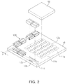
- FIG. 2 is an exploded perspective view of the antenna module shown in FIG. 1 .
- FIG. 3 is a bottom view of the antenna module shown in FIG. 1 .
- FIG. 4 is a cross-sectional view taken along line I-I′ of FIG. 1 .
- FIG. 5 is an enlarged perspective view of the chip antenna shown in FIG. 1 .
- FIG. 6 is a cross-sectional view taken along line Ill l′ of FIG. 5 .
- FIGS. 7 through 10 are perspective views illustrating a chip antenna according to an example.
- FIG. 11 is a perspective view of an antenna module according to an example.
- FIG. 12 is a cross-sectional view of FIG. 11 .
- FIG. 13 is an exploded perspective view of an antenna module according to an example.
- FIG. 14 is a perspective view schematically showing a portable terminal equipped with an antenna module according to an example.
- FIG. 15 is a graph showing the radiation efficiency of the chip antenna shown in FIG. 5 .
- first,” “second,” and “third” may be used herein to describe various members, components, regions, layers, or sections, these members, components, regions, layers, or sections are not to be limited by these terms. Rather, these terms are only used to distinguish one member, component, region, layer, or section from another member, component, region, layer, or section. Thus, a first member, component, region, layer, or section referred to in examples described herein may also be referred to as a second member, component, region, layer, or section without departing from the teachings of the examples.
- spatially relative terms such as “above,” “upper,” “below,” and “lower” may be used herein for ease of description to describe one element's relationship to another element as shown in the figures. Such spatially relative terms are intended to encompass different orientations of the device in use or operation in addition to the orientation depicted in the figures. For example, if the device in the figures is turned over, an element described as being “above” or “upper” relative to another element will then be “below” or “lower” relative to the other element. Thus, the term “above” encompasses both the above and below orientations depending on the spatial orientation of the device.
- the device may also be oriented in other ways (for example, rotated 90 degrees or at other orientations), and the spatially relative terms used herein are to be interpreted accordingly.
- An example of an antenna module described herein may operate in a high frequency domain and operate in a millimeter wave communications band.
- a chip antenna module may operate in a frequency band between 20 GHz and 60 GHz.
- the examples of antenna modules described herein may also be mounted on an electronic device configured to receive or transmit wireless signals.
- a chip antenna may be mounted on a portable telephone, a portable notebook, a drone or the like.
- FIG. 1 is a plan view of an antenna module 1 according to an example.
- FIG. 2 is an exploded perspective view of the antenna module 1 shown in FIG. 1 .
- FIG. 3 is a bottom view of the antenna module 1 shown in FIG. 1 .
- FIG. 4 is a cross-sectional view taken along line I-I′ of FIG. 1 .
- the antenna module 1 includes a substrate 10 , an electronic element 50 , and a chip antenna 100 .
- the substrate 10 may be a circuit board on which a circuit or electronic parts necessary for a wireless antenna is mounted.
- the substrate 10 may be a PCB that accommodates one or more electronic parts therein or one or more electronic parts mounted on a surface.
- the substrate 10 may be provided with a circuit wiring electrically connecting electronic parts.
- the substrate 10 may be a multilayer substrate in which a plurality of insulating layers 17 and a plurality of wiring layers 16 are repeatedly stacked. However, it is also possible to use a double-sided board having wiring layers 16 formed on both sides of one insulating layer 17 .
- a material of the insulating layer 17 is not particularly limited.
- a thermosetting resin such as an epoxy resin, a thermoplastic resin such as polyimide, or a resin impregnated with these resin and a core material such as glass fiber (glass fiber, glass cloth, and glass fabric) together with an inorganic filler
- an insulating material such as a prepreg, an Ajinomoto Build-up Film (ABF), FR-4, or bismaleimide triazine (BT) may be used.
- a photo imagable dielectric (PID) resin may be used.
- the wiring layer 16 electrically connects an electronic element 50 and antennas 90 and 100 . Also, the wiring layer 16 electrically connects the electronic element 50 or the antennas 90 and 100 externally.
- the material of the wiring layer 16 copper (Cu), aluminum (Al), silver (Ag), tin (Sn), gold (Au), nickel (Ni), lead (Pb), titanium (Ti) or a conductive material such as an alloy thereof may be used.
- Interlayer connection conductors 18 for interconnecting the wiring layers 16 to be stacked are arranged inside the insulating layer 17 .
- An insulating protective layer 19 may also be disposed on the surface of the substrate 10 .
- the insulating protective layer 19 is disposed to cover both the insulating layer 17 and the wiring layer 16 on the upper surface and the lower surface of the insulating layer 17 .
- the insulating protective layer 19 protects the wiring layer 16 disposed on the upper surface or the lower surface of the insulating layer 17 .
- the insulating protective layer 19 may have an opening exposing at least a part of the wiring layer 16 .
- the insulating protective layer 19 includes an insulating resin and an inorganic filler, but may not include glass fiber.
- a solder resist may be used as the insulating protective layer 19 , but the disclosure is not limited to such a configuration.
- the substrate 10 various kinds of substrates (for example, a printed circuit board, a flexible substrate, a ceramic substrate, a glass substrate, etc.) well known in the art may also be used.
- substrates for example, a printed circuit board, a flexible substrate, a ceramic substrate, a glass substrate, etc.
- a first surface, an upper surface of the substrate 10 may be divided into an element mounting portion 11 a , a ground region 11 b , and a feeder region 11 c.
- the element mounting portion 11 a is disposed inside of the ground region 11 b as a region in which the electronic element 50 is mounted.
- a plurality of connection pads 12 a to which the electronic element 50 is electrically connected are arranged in the element mounting portion 11 a.
- the ground region 11 b is a region in which a ground layer 16 a is disposed and is disposed to surround the element mounting portion 11 a . Therefore, the element mounting portion 11 a is disposed inside of the ground region 11 b.
- one of the wiring layers 16 of the substrate 10 may be used as the ground layer 16 a . Therefore, the ground layer 16 a may be disposed on the upper surface of the insulating layer 17 or between two stacked insulating layers 17 .
- the element mounting portion 11 a is formed in a rectangular shape. Therefore, the ground region 11 b is disposed to surround the element mounting portion 11 a in the form of a square ring.
- the disclosure is not limited to such a configuration.
- connection pad 12 a of the element mounting portion 11 a is electrically connected to outside or other components through the interlayer connection conductor 18 passing through the insulating layer 17 of the substrate 10 .
- a plurality of ground pads 12 b are formed in the ground region 11 b .
- the ground pad 12 b may be formed by partially opening the insulating protective layer 19 covering the ground layer 16 a . Therefore, in this case, the ground pad 12 b is configured as a part of the ground layer 16 a .
- the disclosure is not limited to such a configuration.
- the ground pad 12 b may be disposed on the upper surface of the insulating layer 17 , and the ground pad 12 b and the ground layer 16 a may be connected through the interlayer connection conductors 18 .
- the ground pad 12 b is disposed to be paired with a feeder pad 12 c . Therefore, the ground pad 12 b is disposed at a position adjacent to the feeder pad 12 c.
- the feeder region 11 c is disposed outside the ground region 11 b .
- the feeder region 11 c is formed outside of two sides formed by the ground region 11 b . Therefore, the feeder region 11 c is disposed along the edge of the substrate 10 .
- the disclosure is not limited to such a configuration.
- a plurality of feeder pads 12 c are disposed in the feeder region 11 c .
- the feeder pad 12 c is disposed on the upper surface of the insulating layer 17 and a radiation portion 130 a of the chip antenna 100 is bonded thereto.
- the feeder pad 12 c is electrically connected to the electronic element 50 and other components via the interlayer connection conductor 18 and the wiring layer 16 that penetrate the insulating layer 17 of the substrate 10 .
- connection pad 12 a , the ground pad 12 b and the feeder pads 12 c are exposed externally in the form of a pad through openings from which the insulating protective layer 19 is removed.
- the feeder pad 12 c is formed to have a smaller area (surface area) than the lower surface (or a bonding surface) of the radiation portion 130 a of the chip antenna 100 .
- the area (surface area) of the feeder pad 12 c may be less than half the area (surface area) of the lower surface (or the bonding surface) of the radiation portion 130 a of the chip antenna 100 .
- the feeder pad 12 c is not bonded to the entire lower surface of the radiation portion 130 a but is bonded to only a part of the lower surface of the radiation portion 130 a.
- the feeder pad 12 c of the present example is formed in a rectangular shape, and the longest side is formed to have a length equal to or greater than a width W 2 of the radiation portion 130 a.
- each two of the feeder pads 12 c are also arranged in pairs. Referring to FIG. 1 , a total of four feeder pads 12 c are each two arranged in pairs. However, the disclosure is not limited to such a configuration. The number of pairs formed by the feeder pads 12 c may be changed according to the size of a module or the like.
- the paired feeder pads 12 c are disposed adjacently to each other. Thus, two chip antennas 100 bonded to the pair of feeder pads 12 c are bonded to the feeder pads 12 c at the end portions of the radiation portions 130 a , respectively.
- the two radiation portions 130 a provided in two adjacent chip antennas 100 are arranged in a line, and are arranged as adjacent as possible at a portion bonded to the feeder pad 12 c.
- the feeder pad 12 c is not limited to the above configuration, and various modifications are possible.
- the feeder pad 12 c may have the same or similar area (surface area) as that of the lower surface of the radiation portion 130 a of the chip antenna 100 . In this case, the reliability of bonding between the chip antenna 100 and the substrate 10 may be improved.
- the feeder pad 12 c is electrically connected to the electronic element 50 via the interlayer connection conductor 18 .
- the interlayer connection conductor 18 extends inside the substrate 10 in a direction perpendicular to the feeder pad 12 c and is connected to the wiring layer 16 inside the substrate 10 .
- a patch antenna 90 is disposed on a second surface, the inner side or the lower surface of the substrate 10 .
- the patch antenna 90 may be configured by the wiring layer 16 provided on the substrate 10 .
- the disclosure is not limited to such a configuration.
- the patch antenna 90 includes a feeder portion 91 including a feeder electrode 92 and a non-feeder electrode 94 .
- the patch antenna 90 includes a plurality of feeder portions 91 dispersedly arranged on the second surface side of the substrate 10 .
- four feeder portions 91 are provided, but the disclosure is not limited to such a configuration.
- the patch antenna 90 is configured such that a part (e.g., a non-feeder electrode) of the patch antenna 90 is disposed on the second surface of the substrate 10 .
- a part e.g., a non-feeder electrode
- the disclosure is not limited to such a configuration, and various configurations are possible, such as disposing the entire patch antenna 90 inside the substrate 10 .
- the feeder electrode 92 is a metal layer having a flat plate shape and is configured as one conductor plate.
- the feeder electrode 92 may have a polygonal structure and is formed in a rectangular shape in the present example. However, various configurations are possible such as the feeder electrode 92 may be formed in a circular shape.
- the feeder electrode 92 may be connected to the electronic element 50 through the interlayer connection conductor 18 .
- the interlayer connection conductor 18 may be connected to the electronic element 50 by penetrating a second ground layer 97 b.
- the non-feeder electrode 94 is disposed spaced by a certain distance from the feeder electrode 92 and is formed as a single flat conductive plate.
- the non-feeder electrode 94 has the same or similar area (surface area) as the feeder electrode 92 .
- the non-feeder electrode 94 may be formed to have a larger area (surface area) than the feeder electrode 92 and disposed to face the entire feeder electrode 92 .
- the non-feeder electrode 94 is disposed on the surface side of the substrate 10 and functions as a director. Thus, the non-feeder electrode 94 may be disposed on the wiring layer 16 disposed at the lowermost portion of the substrate 10 . In this case, the non-feeder electrode 94 is protected by the insulating protective layer 19 disposed on the lower surface of the insulating layer 17 .
- the substrate 10 of the present example also includes a ground structure 95 .
- the ground structure 95 is disposed around the feeder portion 91 and configured in the form of a container accommodating the feeder portion 91 therein.
- the ground structure 95 includes a first ground layer 97 a , a second ground layer 97 b , and a ground via 18 a.
- the first ground layer 97 a is disposed on the same plane as the non-feeder electrode 94 and is disposed around the non-feeder electrode 94 in such a manner as to surround the non-feeder electrode 94 .
- the first ground layer 97 a is spaced apart from the non-feeder electrode 94 by a certain distance.
- the second ground layer 97 b is disposed in a wiring layer 16 different from the first ground layer 97 a .
- the second ground layer 97 b may be disposed between the feeder electrode 92 and the first surface of the substrate 10 .
- the feeder electrode 92 is disposed between the non-feeder electrode 94 and the second ground layer 97 b.
- the second ground layer 97 b may be entirely disposed on the corresponding wiring layer 16 and may be partially removed only in a portion in which the interlayer connection conductor 18 connected to the feeder electrode 92 is disposed.
- the ground via 18 a is an interlayer connection conductor that electrically connects the first ground layer 97 a and the second ground layer 97 b and is arranged as a plurality of ground vias in such a manner as to surround the feeder portion 91 along the circumference of the feeder portion 91 .
- the ground vias 18 a are arranged in a single row.
- various configurations are possible, such as the ground vias 18 a being arranged in a plurality of rows.
- the feeder portion 91 is disposed in the ground structure 95 formed in the shape of the container by the first ground layer 97 a , the second ground layer 97 b , and the ground via 18 a .
- the plurality of ground vias 18 a arranged in a line define side surfaces in the shape of the container.
- Each of the feeder portions 91 of the present example is disposed in the shape of the container. Therefore, the interference between the feeder portions 91 is blocked by the ground structure 95 .
- noise transmitted in the horizontal direction of the substrate 10 may be blocked by the side surface in the shape of the container configured by the plurality of ground vias 18 a.
- the feeder portion 91 is isolated from the adjacent other feeder portions 91 . Further, since the ground structure 95 in the shape of the container serves as a reflector, the radiation characteristic of the patch antenna 90 may be enhanced.
- the feeder portion 91 of the patch antenna 90 emits a radio signal in the thickness direction (e.g., the lower direction) of the substrate 10 .
- the first ground layer 97 a and the second ground layer 97 b in the present example are not disposed in a region facing the feeder region ( 11 c in FIG. 2 ) defined on the first surface of the substrate 10 . This is for the purpose of minimizing interference between the radio signal radiated from the chip antenna and the ground structure 95 , but is not limited thereto.
- the patch antenna 90 includes the feeder electrode 92 and the non-feeder electrode 94 .
- the patch antenna 90 may be configured to include only the feeder electrode 92 .
- the electronic element 50 is mounted on the element mounting portion 11 a of the substrate 10 .
- the electronic element 50 may be bonded to a connection pad 12 a of the element mounting portion 11 a via a conductive adhesive.
- one electronic element 50 is mounted on the element mounting portion 11 a .
- a plurality of electronic elements 50 may be mounted on the element mounting portion 11 a.
- the electronic element 50 includes at least one active element, and may include, for example, a signal processing element applying a feeder signal to the radiation portion 130 a of the antenna.
- the electronic element 50 may also include a passive element.
- the chip antenna 100 is used in wireless communications in a gigahertz frequency band and is mounted on the substrate 10 to receive a feeder signal from the electronic element 50 and radiate it externally.
- the chip antenna 100 is formed in a hexahedral shape as a whole and has both ends connected to the feeder pad 12 c and the ground pad 12 b of the substrate 10 respectively via a conductive adhesive such as solder and mounted on the substrate 10 .
- FIG. 5 is an enlarged perspective view of the chip antenna 100 shown in FIG. 1 .
- FIG. 6 is a cross-sectional view taken along line I-I′ of FIG. 5 .
- the chip antenna 100 includes a body portion 120 , a radiation portion 130 a , and a ground portion 130 b.
- the body portion 120 has a hexahedral shape and is formed of a dielectric substance.
- the body portion 120 may be formed of a polymer having a dielectric constant or a ceramic sintered body.
- the chip antenna 100 according to the present example is a chip antenna used in a 3 GHz to 30 GHz band.
- a wavelength A of the electromagnetic wave from 3 GHz to 30 GHz is 100 mm to 0.75 mm, and the length of the antenna is theoretically ⁇ , ⁇ /2, and ⁇ /4. Therefore, the length of a radiation antenna should be approximately 50 mm to 25 mm. However, when the body portion 120 is formed of a material having a dielectric constant higher than that of air, the length thereof may be remarkably reduced.
- the chip antenna 100 of the present example configures the body portion 120 formed of a material having a dielectric constant of 3.5 to 25.
- the maximum length of the chip antenna 100 may be manufactured within a range of 0.5 to 2 mm.
- the dielectric constant of the body portion 120 is less than 3.5, a distance between the radiation portion 130 a and the ground portion 130 b must be increased in order for the chip antenna 100 to operate normally.
- the chip antenna 100 is measured to function normally in the 3 GHz ⁇ 30 GHz band only at the maximum width W of 2 mm or more.
- the overall size of the chip antenna 100 is increased, it is difficult to mount the chip antenna 100 on a thin portable device.
- the length of the longest side of the chip antenna 100 of the present example is 2 mm or less in consideration of the wavelength length and the mounting size.
- the chip antenna 100 according to the present example may have a length of the longest side of 0.5 to 2 mm.
- the size of the chip antenna 100 should be reduced to 0.3 mm or less. In this case, the performance of the antenna is measured to be rather degraded.
- the body portion 120 of the chip antenna 100 according to the present example is formed of a dielectric having a dielectric constant of 3.5 or more and 25 or less.
- the radiation portion 130 a is coupled to a first surface of the body portion 120 .
- the ground portion 130 b is coupled to a second surface of the body portion 120 .
- the first surface and the second surface refer to two surfaces facing each other in the body portion 120 formed as a hexahedron.
- the width W 1 of the body portion 120 is defined as a distance between the first surface and the second surface.
- a direction toward the second surface from the first surface of the body portion 120 (or a direction from the second surface toward the first surface of the body portion 120 ) is defined as a width direction of the body portion 120 or the chip antenna 100 .
- the widths W 2 and W 3 of the radiation portion 130 a and the ground portion 130 b are defined as distances in the width direction of the chip antenna 100 .
- the width W 2 of the radiation portion 130 a means the shortest distance from a bonding surface of the radiation portion 130 a bonded to the first surface of the body portion 120 to an opposite surface of the bonding surface
- the width W 3 of the first portion 130 b means the shortest distance from a bonding surface of the ground portion 130 b bonded to the second surface of the body portion 120 to an opposite surface of the bonding surface.
- the radiation portion 130 a is in contact with only one of the six surfaces of the body portion 120 and is coupled to the body portion 120 .
- the ground portion 130 b is in contact with only one of the six surfaces of the body portion 120 and is coupled to the body portion 120 .
- the radiation portion 130 a and the ground portion 130 b are not disposed on surfaces other than the first and second surfaces of the body portion 120 , but are arranged parallel to each other with the body portion 120 interposed therebetween.
- a radiation portion and a ground portion are arranged in the form of a thin film on a lower surface of the body portion.
- a distance between the radiation portion and the ground portion is small and thus the radiation portion and the ground portion are close to each other, a loss due to inductance occurs.
- accurate capacitance may not be predicted, and it is difficult to adjust a resonance point, which makes tuning of the impedance difficult.
- the radiation portion 130 a and the ground portion 130 b are formed in a block shape and are coupled to a first surface and a second surface of the body portion 120 , respectively.
- the radiation portion 130 a and the ground portion 130 b are each formed in a hexahedral shape, and one surface of the hexahedron is bonded to each of a first surface and a second surface of the body portion 120 .
- the chip antenna 100 of the present disclosure has capacitance due to a dielectric substance (for example, a body portion) between the radiation portion 130 a and the ground portion 130 b , it is possible to design a coupling antenna or to adjust a resonance frequency by using the capacitance.
- a dielectric substance for example, a body portion
- the radiation portion 130 a and the ground portion 130 b may be formed of the same material.
- the radiation portion 130 a and the ground portion 130 b may be formed to have the same shape and the same structure. In this case, the radiation portion 130 a and the ground portion 130 b may be classified according to a type of a pad to be bonded when mounted on the substrate 10 .
- a portion of the substrate 10 bonded to the feeder pad 12 c of the substrate 10 may function as the radiation portion 130 a
- a portion of the substrate 10 bonded to the ground pad 12 b may function as the ground portion 130 b
- the disclosure is not limited to such a configuration.
- the radiation portion 130 a and the ground portion 130 b include a first conductor 131 and a second conductor 132 .
- the first conductor 131 is a conductor directly bonded to the body portion 120 and is formed in a block shape.
- the second conductor 132 is formed in the form of a layer along a surface of the first conductor 131 .
- the first conductor 131 is formed on one surface of the body portion 120 through a printing process or a plating process and may be formed of one kind or two or more kinds of alloy selected from the group consisting of Ag, Au, Cu, Al, Pt, Ti, Mo, Ni, and W.
- the first conductor 131 may be also formed of a conductive paste or a conductive epoxy in which an organic material such as a polymer or a glass is contained in metal.
- the second conductor 132 may be formed on the surface of the first conductor 131 through a plating process.
- the second conductor 132 may be formed by sequentially stacking a nickel (Ni) layer and a tin (Sn) layer, or by sequentially stacking a zinc (Zn) layer and a tin (Sn) layer.
- a thickness t 2 of the radiation portion 130 a and the ground portion 130 b is formed to be greater than a thickness t 1 of the body portion 120 .
- a length d 2 of the radiation portion 130 a and the ground portion 130 b is also greater than a length d 1 of the body portion 120 .
- the first conductor 131 is formed to have the same thickness and the same length as the thickness t 1 and length d 1 of the body portion 120 .
- the radiation portion 130 a and the ground portion 130 b are formed to be longer than the body portion 120 by virtue of the second conductor 132 formed on the surface of the first conductor 131 .
- FIG. 15 is a graph showing the radiation efficiency of a chip antenna shown in FIG. 5 , wherein the widths W 2 and W 3 of the radiation portion 130 a and the ground portion 130 b are increased in a 28 GHz band, and a reflection loss S 11 of the chip antenna is measured.
- the chip antenna used for measurement is measured by fixing the width W 1 of the body portion 120 of 1 mm, the thickness t 2 of the radiation portion 130 a and the ground portion 130 b of 0.6 mm, and the length d 2 of 1.3 mm, and varying only the widths W 2 and W 3 .
- the reflection loss S 11 of the chip antenna according to the example decreases as the widths W 2 and W 3 of the radiation portion 130 a and the ground portion 130 b increase. It is measured that the reflection loss S 11 decreases at a high reduction rate in a section where the widths W 2 and W 3 of the radiation portion 130 a and the ground portion 130 b are less than or equal to 100 ⁇ m and the reflection loss S 11 decreases at a relatively low reduction rate in a section where the widths W 2 and W 3 exceed 100 ⁇ m.
- the width W 1 of the body portion 120 is 1 mm in the example
- the width W 2 of the radiation portion 130 a and the width W 3 of the ground portion 130 b are defined to be equal to or more than 100 ⁇ m.
- the chip antenna according to the example satisfies Equation 1 below with respect to the width W 1 of the body portion 120 and the width W 2 of the radiation portion 130 a.
- the maximum widths W 2 and W 3 of the radiation portion 130 a and the ground portion 130 b are defined as 50% or less of the width W 1 of the body portion 120 .
- the maximum length of the chip antenna according to the present example is 2 mm
- the maximum width of the radiation portion 130 a or the ground portion 130 b may be defined as 500 ⁇ m.
- the disclosure is not limited to such a configuration, and the maximum width may be changed when the widths of the radiation portion 130 a and the ground portion 130 b are different from each other.
- the chip antenna according to the examples may be used in a high frequency band equal to or more than 3 GHz less than or equal to 30 GHz and may have a long side having a size less than or equal to 2 mm and may be easily mounted on a thin portable device.
- the radiation portion 130 a and the ground portion 130 b are in contact with only one surface of the body portion 120 , it is easy to tune the resonance frequency, and the antenna radiation efficiency may be maximized by adjusting the antenna volume.
- the chip antenna according to the disclosure is not limited to the above-described configuration, and various configurations are possible.
- FIGS. 7 through 10 are perspective views illustrating a chip antenna according to other examples.
- FIGS. 7 through 9 show chip antennas of various modifications of a shape of the ground portion 130 b .
- the chip antenna shown in FIG. 7 two ground portions 130 b are disposed apart from each other. Accordingly, an empty space is provided between the two ground portions 130 b , and the overall size (length) of the ground portion 130 b is formed to be smaller than the radiation portion 130 a.
- the ground portion 130 b has a length of about half of the radiation portion 130 a , and is disposed at a position inclined to one side on a second surface of the body portion 120 .
- the ground portion 130 b is less than half the length of the radiation portion 130 a , and is centered on the second surface of the body portion 120 .
- the present disclosure is not limited thereto.
- the radiation portion 130 a may be used by modifying a shape of the radiation portion 130 a instead of the ground portion 130 b.
- the ground portion 130 b has a larger volume than the radiation portion 130 a .
- the width W 3 of the ground portion 130 b is formed to be twice as large as the width W 2 of the radiation portion 130 a .
- the width W 2 of the radiation portion 130 a may be greater than the width W 3 of the ground portion 130 b by 50 ⁇ m or more.
- the disclosure is not limited to such a configuration.
- the antenna module according to the examples radiates horizontal polarization using a chip antenna and radiates vertical polarization using a patch antenna. That is, the chip antennas are disposed in a position adjacent to an edge of a substrate to radiate radio waves in a direction (e.g., a planar direction) horizontal to the substrate, and the patch antenna is disposed on a second surface of the substrate to radiate radio waves in a direction (e.g., a thickness direction) vertical to the substrate. Therefore, the radiation efficiency of the radio waves may be increased.
- the patch antenna is disposed on the second surface of the substrate in the examples, various modifications are possible such as the patch antenna being disposed on the first surface of the substrate, and an element mounting portion and the chip antennas being disposed on the second surface of the substrate.
- the two chip antennas 100 are paired and bonded to the two feeder pads 12 c , respectively.
- the two radiation portions 130 a are arranged to be as adjacent as possible to each other at a portion bonded to the feeder pad 12 c , and thus the two chip antennas 100 are a structure of a dipole antenna.
- a distance at which the two chip antennas 100 are spaced apart may be defined as 0.2 mm to 0.5 mm.
- the distance is less than 0.2 mm, interference may occur between the two chip antennas 100 .
- functions of the two chip antennas 100 as the dipole antenna may be degraded.
- the dipole antenna may also be considered to configure the dipole antenna with circuit wiring by using the wiring layer 16 of the substrate 10 instead of the chip antenna 100 .
- the length of the radiation portion 130 a should be a half wavelength of the corresponding frequency, if the dipole antenna is formed by using the wiring layer 16 of the substrate 10 , an area of the substrate 10 occupied by the dipole antenna is relatively large.
- a wavelength is reduced by a dielectric constant of the body portion 120 . Therefore, when the chip antenna 100 is used as in the examples, a distance (P of FIG. 2 ) between the radiation portion 130 a and the ground region 11 b may be reduced through a dielectric constant (e.g. 10 or more) of the body portion 120 . Thus, the area in which the feeder region 11 c or the chip antenna 100 is mounted on the substrate 10 may be minimized.
- a feeder line of the dipole antenna should be spaced by 1 mm or more from a ground region.
- the distance P between the radiation portion 130 a and the ground region 11 b may be designed to be 1 mm or less.
- the size of the feeder region 11 c may be reduced, as compared with the case of using the dipole antenna, and thus the overall size of the antenna module may be minimized.
- the resonance frequency of the chip antenna 100 may be changed. Therefore, in the examples, the radiation portion 130 a of the chip antenna 100 and the ground region 11 b of the substrate 10 may be spaced apart from each other by a range equal to or more than 0.2 mm and less than or equal to 1 mm.
- the chip antenna 100 is disposed at a position not facing the patch antenna along the vertical direction of the substrate 10 .
- the position where the chip antenna 100 does not face the patch antenna along the vertical direction of the substrate 10 means a position where the chip antenna 100 is disposed not to overlap with the patch antenna when the chip antenna 100 is projected on the second surface of the substrate 10 in the vertical direction of the substrate 10 .
- the chip antenna 100 is also disposed not to face the ground structure 95 .
- the present disclosure is not limited thereto, and the chip antenna may be disposed to partially face the ground structure 95 .
- the antenna module according to the present example minimizes the interference between the chip antenna 100 and the patch antenna 90 .
- FIG. 11 is a perspective view of an antenna module according to another example.
- FIG. 12 is a cross-sectional view of FIG. 11 and shows a cross section corresponding to FIG. 4 .
- the antenna module according to the present example includes the substrate 10 , the electronic element 50 , and the chip antenna 100 .
- the electronic element 50 and the chip antenna 100 are similar to those of the above-described examples, and thus detailed descriptions thereof are omitted.
- the substrate 10 of the present example is similar to the above-described example and has a difference in the shape of the ground region 11 b and the feeder region 11 c disposed on a first surface, an upper surface of the substrate 10 .
- the ground region 11 b is disposed on the first surface of the substrate 10 to cover the entire region other than the element mounting portion 11 a .
- the feeder region 11 c is disposed such that the feeder region 11 c partially digs into the ground region 11 b to reduce the width of the ground region 11 b .
- the width of the ground region 11 b means the length of a ground region disposed between the element mounting portion 11 a and the feeder region 11 c.
- the feeder region 11 c is not formed in a continuous linear shape, but is configured such that a plurality of regions are spaced apart along the edge of the substrate 10 .
- the contour of the ground region 11 b is disposed adjacent to the contour of the substrate 10 at a portion where the feeder region 11 c is not disposed.
- the contour of the ground region 11 b may be arranged in the same manner as the contour of the substrate 10 .
- the resonance frequency of the chip antenna 100 may be changed when the distance P between the radiation portion 130 a of the chip antenna 100 and the ground region 11 b is less than 0.2 mm. Therefore, the distance P between the radiation portion 130 a of the chip antenna and the ground region 11 b of the substrate 10 is defined to be 0.2 mm or more. In order to minimize the size of the antenna module, the distance P between the radiation portion 130 a and the ground region 11 b of the substrate 10 may be defined as 1 mm or less.
- the ground region 11 b is also located on a third surface (a surface where the radiation portion and the ground region are both visible) of the chip antenna 100 , the third surface of the chip antenna 100 and the ground region 11 b are also spaced apart in the range equal to or more than 0.2 mm and less than or equal to 1 mm.
- the size of the feeder region 11 c in the present example is defined corresponding to the size of the chip antenna 100 .
- the patch antenna 90 is not dependent on the size or shape of the feeder region 11 c . Therefore, the patch antenna 90 of the present example may be disposed irrespective of the position of the feeder region 11 c.
- the antenna module according to the present example may minimize the size of the feeder region 11 c and reduce the overall size of the antenna module.
- FIG. 13 is an exploded perspective view of an antenna module according to another example.
- the antenna module according to the present example is configured to be similar to an antenna substrate shown in FIG. 2 , and has a difference in the structure of the feeder pad 12 c.
- the feeder pad 12 c of the present example is formed to have the same or similar area (surface area) as that of a lower surface of the radiation portion 130 a of the chip antenna 100 .
- the area (surface area) of the feeder pad 12 c may be in the range of 80% to 120% of the area (surface area) of the lower surface of the radiation portion 130 a of the chip antenna 100 .
- the disclosure is not limited to such a configuration.
- a pair of two feeder pads 12 c are linearly formed and are spaced apart such that end portions face each other on a straight line.
- the area (surface area) of the feeder pad 12 c is configured to be similar to the area of the lower surface of the radiation portion 130 a of the chip antenna 100 , the reliability of bonding between the chip antenna 100 and the substrate 10 may be increased.
- the interlayer connection conductors 18 b (hereinafter, feeder vias) connected to the feeder pads 12 c in the present example are respectively disposed at the end portions of the feeder pads 12 c .
- the feeder via 18 b extends into the substrate 10 in a direction perpendicular to the feeder pad 12 c and is connected to the wiring layer 16 inside the substrate 10 .
- Two feeder pads 12 c are arranged in pairs. Therefore, two feeder vias 18 b connected to the feeder pads 12 c are also arranged in pairs.
- the pair of two feeder vias 18 b are disposed at the end portions at which the pair of two feeder pads 12 c face each other.
- the feeder vias 18 b may be arranged as close as possible.
- a distance between the two feeder vias 18 b may be the same as or similar to the distance between the pair of two feeder pads 12 c.
- FIG. 14 is a perspective view schematically showing a portable terminal 200 equipped with antenna modules 1 of the examples.
- the antenna modules 1 are disposed at corners of the portable terminal 200 .
- the antenna modules 1 are disposed such that the chip antenna 100 is adjacent to the corners of the portable terminal 200 .
- the antenna modules 1 are disposed at all of four corners of the portable terminal 200 .
- the arrangement structure of the antenna modules 1 may be variously modified, such as when an internal space of the portable terminal 200 is insufficient, only two antenna modules 1 are arranged in a diagonal direction of the portable terminal 200 .
- the antenna modules 1 are coupled to the portable terminal 200 such that a feeder region is disposed adjacent to the edge of the portable terminal 200 . Accordingly, radio waves radiated through a chip antenna of the antenna module 1 are radiated toward the outside of the portable terminal 200 in the surface direction of the portable terminal 200 . Radio waves radiated through a patch antenna of the antenna module 1 are radiated in the thickness direction of the portable terminal 200 .
- an antenna module of the present disclosure uses a chip antenna instead of a wiring type dipole antenna, and thus the module size may be minimized. Also, the transmission/reception efficiency may be improved.
Landscapes
- Engineering & Computer Science (AREA)
- Computer Networks & Wireless Communication (AREA)
- Physics & Mathematics (AREA)
- Electromagnetism (AREA)
- Microelectronics & Electronic Packaging (AREA)
- Computer Hardware Design (AREA)
- General Engineering & Computer Science (AREA)
- Waveguide Aerials (AREA)
- Details Of Aerials (AREA)
Abstract
Description
W2/W1≥1/10 (Equation 1)
Claims (25)
Priority Applications (1)
| Application Number | Priority Date | Filing Date | Title |
|---|---|---|---|
| US17/177,512 US11637362B2 (en) | 2017-12-14 | 2021-02-17 | Antenna module |
Applications Claiming Priority (4)
| Application Number | Priority Date | Filing Date | Title |
|---|---|---|---|
| KR20170172322 | 2017-12-14 | ||
| KR10-2017-0172322 | 2017-12-14 | ||
| KR1020180061995A KR102520432B1 (en) | 2017-12-14 | 2018-05-30 | Antenna module |
| KR10-2018-0061995 | 2018-05-30 |
Related Child Applications (1)
| Application Number | Title | Priority Date | Filing Date |
|---|---|---|---|
| US17/177,512 Continuation US11637362B2 (en) | 2017-12-14 | 2021-02-17 | Antenna module |
Publications (2)
| Publication Number | Publication Date |
|---|---|
| US20190190120A1 US20190190120A1 (en) | 2019-06-20 |
| US10965007B2 true US10965007B2 (en) | 2021-03-30 |
Family
ID=66816396
Family Applications (2)
| Application Number | Title | Priority Date | Filing Date |
|---|---|---|---|
| US16/149,440 Active 2039-05-22 US10965007B2 (en) | 2017-12-14 | 2018-10-02 | Antenna module |
| US17/177,512 Active 2039-01-02 US11637362B2 (en) | 2017-12-14 | 2021-02-17 | Antenna module |
Family Applications After (1)
| Application Number | Title | Priority Date | Filing Date |
|---|---|---|---|
| US17/177,512 Active 2039-01-02 US11637362B2 (en) | 2017-12-14 | 2021-02-17 | Antenna module |
Country Status (2)
| Country | Link |
|---|---|
| US (2) | US10965007B2 (en) |
| CN (1) | CN109962334A (en) |
Cited By (1)
| Publication number | Priority date | Publication date | Assignee | Title |
|---|---|---|---|---|
| US11018418B2 (en) * | 2018-01-31 | 2021-05-25 | Samsung Electro-Mechanics Co., Ltd. | Chip antenna and chip antenna module including the same |
Families Citing this family (9)
| Publication number | Priority date | Publication date | Assignee | Title |
|---|---|---|---|---|
| KR102607538B1 (en) * | 2019-08-08 | 2023-11-28 | 삼성전기주식회사 | Antenna apparatus |
| KR102603106B1 (en) * | 2019-09-04 | 2023-11-15 | 삼성전기주식회사 | Array antenna |
| US11133578B2 (en) * | 2019-09-06 | 2021-09-28 | Nxp B.V. | Semiconductor device package comprising an encapsulated and conductively shielded semiconductor device die that provides an antenna feed to a waveguide |
| US11916007B2 (en) * | 2019-10-23 | 2024-02-27 | Infineon Technologies Ag | Semiconductor device with embedded flexible circuit |
| CN113206372B (en) | 2020-01-31 | 2025-06-24 | 沐风电子科技(广州)有限公司 | Array antenna device and manufacturing method thereof and electronic equipment |
| US12142856B2 (en) * | 2020-07-08 | 2024-11-12 | Samsung Electro-Mechanics Co., Ltd. | Multilayer dielectric resonator antenna and antenna module |
| TWI789877B (en) * | 2021-08-19 | 2023-01-11 | 特崴光波導股份有限公司 | Antenna structure |
| CN116031629A (en) * | 2021-10-25 | 2023-04-28 | 深南电路股份有限公司 | Antenna module, preparation method of antenna module and terminal |
| US12126071B2 (en) * | 2022-03-01 | 2024-10-22 | Qualcomm Incorporated | Multi-directional antenna modules employing a surface-mount antenna(s) to support antenna pattern multi-directionality, and related fabrication methods |
Citations (8)
| Publication number | Priority date | Publication date | Assignee | Title |
|---|---|---|---|---|
| JP2000232315A (en) | 1999-02-08 | 2000-08-22 | Murata Mfg Co Ltd | Anttena system and radio equipment mounting the same |
| US20090040120A1 (en) * | 2006-09-20 | 2009-02-12 | Murata Manufacturing Co., Ltd. | Antenna structure and radio communication device using the same |
| WO2009110679A1 (en) | 2008-03-06 | 2009-09-11 | 주식회사 감마누 | Board-shaped wideband dual polarization antenna |
| US20110102289A1 (en) * | 2009-11-05 | 2011-05-05 | Leem Jihun | Portable terminal |
| US8570234B2 (en) | 2010-05-31 | 2013-10-29 | Inpaq Technology Co., Ltd. | Assembly of chip antenna and circuit board |
| WO2014129754A1 (en) | 2013-02-20 | 2014-08-28 | 엘에스전선 주식회사 | Dipole antenna |
| US20150070228A1 (en) * | 2013-09-11 | 2015-03-12 | International Business Machines Corporation | Antenna-in-package structures with broadside and end-fire radiations |
| US20180048075A1 (en) * | 2016-08-10 | 2018-02-15 | Samsung Electronics Co., Ltd. | Antenna device and electronic device including the same |
Family Cites Families (6)
| Publication number | Priority date | Publication date | Assignee | Title |
|---|---|---|---|---|
| FI118748B (en) * | 2004-06-28 | 2008-02-29 | Pulse Finland Oy | Chip antenna |
| KR100638726B1 (en) * | 2005-02-25 | 2006-10-30 | 삼성전기주식회사 | Antenna module and electronic device having same |
| JP4384102B2 (en) | 2005-09-13 | 2009-12-16 | 株式会社東芝 | Portable radio device and antenna device |
| KR100930618B1 (en) * | 2009-02-09 | 2009-12-09 | (주)파트론 | Built-in chip antenna structure in the form of a double parallel plate |
| CN102959797A (en) * | 2010-07-16 | 2013-03-06 | 株式会社村田制作所 | Antenna device |
| CN202905935U (en) * | 2012-11-16 | 2013-04-24 | 成都成电电子信息技术工程有限公司 | Small high-performance chip antenna |
-
2018
- 2018-10-02 US US16/149,440 patent/US10965007B2/en active Active
- 2018-12-03 CN CN201811465059.2A patent/CN109962334A/en active Pending
-
2021
- 2021-02-17 US US17/177,512 patent/US11637362B2/en active Active
Patent Citations (9)
| Publication number | Priority date | Publication date | Assignee | Title |
|---|---|---|---|---|
| JP2000232315A (en) | 1999-02-08 | 2000-08-22 | Murata Mfg Co Ltd | Anttena system and radio equipment mounting the same |
| US20090040120A1 (en) * | 2006-09-20 | 2009-02-12 | Murata Manufacturing Co., Ltd. | Antenna structure and radio communication device using the same |
| WO2009110679A1 (en) | 2008-03-06 | 2009-09-11 | 주식회사 감마누 | Board-shaped wideband dual polarization antenna |
| US20110043424A1 (en) | 2008-03-06 | 2011-02-24 | Gamma Nu, Inc. | Board-shaped wideband dual polarization antenna |
| US20110102289A1 (en) * | 2009-11-05 | 2011-05-05 | Leem Jihun | Portable terminal |
| US8570234B2 (en) | 2010-05-31 | 2013-10-29 | Inpaq Technology Co., Ltd. | Assembly of chip antenna and circuit board |
| WO2014129754A1 (en) | 2013-02-20 | 2014-08-28 | 엘에스전선 주식회사 | Dipole antenna |
| US20150070228A1 (en) * | 2013-09-11 | 2015-03-12 | International Business Machines Corporation | Antenna-in-package structures with broadside and end-fire radiations |
| US20180048075A1 (en) * | 2016-08-10 | 2018-02-15 | Samsung Electronics Co., Ltd. | Antenna device and electronic device including the same |
Cited By (1)
| Publication number | Priority date | Publication date | Assignee | Title |
|---|---|---|---|---|
| US11018418B2 (en) * | 2018-01-31 | 2021-05-25 | Samsung Electro-Mechanics Co., Ltd. | Chip antenna and chip antenna module including the same |
Also Published As
| Publication number | Publication date |
|---|---|
| US20190190120A1 (en) | 2019-06-20 |
| US11637362B2 (en) | 2023-04-25 |
| US20210175612A1 (en) | 2021-06-10 |
| CN109962334A (en) | 2019-07-02 |
Similar Documents
| Publication | Publication Date | Title |
|---|---|---|
| US11637362B2 (en) | Antenna module | |
| US11211689B2 (en) | Chip antenna | |
| US10938091B1 (en) | Chip antenna | |
| US11069954B2 (en) | Chip antenna | |
| US10978785B2 (en) | Chip antenna module | |
| US10965004B2 (en) | Chip antenna module | |
| KR102382241B1 (en) | Chip antenna and chip antenna module having the same | |
| US11431097B2 (en) | Chip antenna module | |
| US11139551B2 (en) | Chip antenna module | |
| US11050154B2 (en) | Chip antenna | |
| KR102565122B1 (en) | Chip antenna module | |
| KR102520432B1 (en) | Antenna module | |
| KR102500007B1 (en) | Chip antenna module | |
| KR20190093103A (en) | Chip antenna and chip antenna module having the same |
Legal Events
| Date | Code | Title | Description |
|---|---|---|---|
| AS | Assignment |
Owner name: SAMSUNG ELECTRO-MECHANICS CO., LTD., KOREA, REPUBL Free format text: ASSIGNMENT OF ASSIGNORS INTEREST;ASSIGNORS:KIM, JAE YEONG;AN, SUNG YONG;CHOI, CHANG HAK;REEL/FRAME:047036/0649 Effective date: 20181001 Owner name: SAMSUNG ELECTRO-MECHANICS CO., LTD., KOREA, REPUBLIC OF Free format text: ASSIGNMENT OF ASSIGNORS INTEREST;ASSIGNORS:KIM, JAE YEONG;AN, SUNG YONG;CHOI, CHANG HAK;REEL/FRAME:047036/0649 Effective date: 20181001 |
|
| FEPP | Fee payment procedure |
Free format text: ENTITY STATUS SET TO UNDISCOUNTED (ORIGINAL EVENT CODE: BIG.); ENTITY STATUS OF PATENT OWNER: LARGE ENTITY |
|
| STPP | Information on status: patent application and granting procedure in general |
Free format text: DOCKETED NEW CASE - READY FOR EXAMINATION |
|
| STPP | Information on status: patent application and granting procedure in general |
Free format text: NON FINAL ACTION MAILED |
|
| STPP | Information on status: patent application and granting procedure in general |
Free format text: RESPONSE TO NON-FINAL OFFICE ACTION ENTERED AND FORWARDED TO EXAMINER |
|
| STPP | Information on status: patent application and granting procedure in general |
Free format text: PUBLICATIONS -- ISSUE FEE PAYMENT VERIFIED |
|
| STCF | Information on status: patent grant |
Free format text: PATENTED CASE |
|
| MAFP | Maintenance fee payment |
Free format text: PAYMENT OF MAINTENANCE FEE, 4TH YEAR, LARGE ENTITY (ORIGINAL EVENT CODE: M1551); ENTITY STATUS OF PATENT OWNER: LARGE ENTITY Year of fee payment: 4 |