US10964730B2 - Non-contact measurement of a stress in a film on a substrate - Google Patents
Non-contact measurement of a stress in a film on a substrate Download PDFInfo
- Publication number
- US10964730B2 US10964730B2 US16/741,628 US202016741628A US10964730B2 US 10964730 B2 US10964730 B2 US 10964730B2 US 202016741628 A US202016741628 A US 202016741628A US 10964730 B2 US10964730 B2 US 10964730B2
- Authority
- US
- United States
- Prior art keywords
- substrate
- thin
- topography data
- film
- stress
- Prior art date
- Legal status (The legal status is an assumption and is not a legal conclusion. Google has not performed a legal analysis and makes no representation as to the accuracy of the status listed.)
- Active
Links
Images


Classifications
-
- H—ELECTRICITY
- H10—SEMICONDUCTOR DEVICES; ELECTRIC SOLID-STATE DEVICES NOT OTHERWISE PROVIDED FOR
- H10D—INORGANIC ELECTRIC SEMICONDUCTOR DEVICES
- H10D86/00—Integrated devices formed in or on insulating or conducting substrates, e.g. formed in silicon-on-insulator [SOI] substrates or on stainless steel or glass substrates
- H10D86/01—Manufacture or treatment
- H10D86/021—Manufacture or treatment of multiple TFTs
- H10D86/0212—Manufacture or treatment of multiple TFTs comprising manufacture, treatment or coating of substrates
-
- H01L27/1262—
-
- G—PHYSICS
- G01—MEASURING; TESTING
- G01B—MEASURING LENGTH, THICKNESS OR SIMILAR LINEAR DIMENSIONS; MEASURING ANGLES; MEASURING AREAS; MEASURING IRREGULARITIES OF SURFACES OR CONTOURS
- G01B11/00—Measuring arrangements characterised by the use of optical techniques
- G01B11/02—Measuring arrangements characterised by the use of optical techniques for measuring length, width or thickness
- G01B11/06—Measuring arrangements characterised by the use of optical techniques for measuring length, width or thickness for measuring thickness ; e.g. of sheet material
- G01B11/0608—Height gauges
-
- G—PHYSICS
- G01—MEASURING; TESTING
- G01B—MEASURING LENGTH, THICKNESS OR SIMILAR LINEAR DIMENSIONS; MEASURING ANGLES; MEASURING AREAS; MEASURING IRREGULARITIES OF SURFACES OR CONTOURS
- G01B11/00—Measuring arrangements characterised by the use of optical techniques
- G01B11/16—Measuring arrangements characterised by the use of optical techniques for measuring the deformation in a solid, e.g. optical strain gauge
-
- G—PHYSICS
- G01—MEASURING; TESTING
- G01B—MEASURING LENGTH, THICKNESS OR SIMILAR LINEAR DIMENSIONS; MEASURING ANGLES; MEASURING AREAS; MEASURING IRREGULARITIES OF SURFACES OR CONTOURS
- G01B11/00—Measuring arrangements characterised by the use of optical techniques
- G01B11/24—Measuring arrangements characterised by the use of optical techniques for measuring contours or curvatures
-
- G—PHYSICS
- G01—MEASURING; TESTING
- G01B—MEASURING LENGTH, THICKNESS OR SIMILAR LINEAR DIMENSIONS; MEASURING ANGLES; MEASURING AREAS; MEASURING IRREGULARITIES OF SURFACES OR CONTOURS
- G01B11/00—Measuring arrangements characterised by the use of optical techniques
- G01B11/30—Measuring arrangements characterised by the use of optical techniques for measuring roughness or irregularity of surfaces
-
- G—PHYSICS
- G01—MEASURING; TESTING
- G01L—MEASURING FORCE, STRESS, TORQUE, WORK, MECHANICAL POWER, MECHANICAL EFFICIENCY, OR FLUID PRESSURE
- G01L1/00—Measuring force or stress, in general
- G01L1/24—Measuring force or stress, in general by measuring variations of optical properties of material when it is stressed, e.g. by photoelastic stress analysis using infrared, visible light, ultraviolet
-
- G—PHYSICS
- G01—MEASURING; TESTING
- G01M—TESTING STATIC OR DYNAMIC BALANCE OF MACHINES OR STRUCTURES; TESTING OF STRUCTURES OR APPARATUS, NOT OTHERWISE PROVIDED FOR
- G01M11/00—Testing of optical apparatus; Testing structures by optical methods not otherwise provided for
- G01M11/08—Testing mechanical properties
- G01M11/081—Testing mechanical properties by using a contact-less detection method, i.e. with a camera
-
- G—PHYSICS
- G01—MEASURING; TESTING
- G01R—MEASURING ELECTRIC VARIABLES; MEASURING MAGNETIC VARIABLES
- G01R31/00—Arrangements for testing electric properties; Arrangements for locating electric faults; Arrangements for electrical testing characterised by what is being tested not provided for elsewhere
- G01R31/26—Testing of individual semiconductor devices
- G01R31/2648—Characterising semiconductor materials
-
- H01L21/16—
-
- H—ELECTRICITY
- H01—ELECTRIC ELEMENTS
- H01L—SEMICONDUCTOR DEVICES NOT COVERED BY CLASS H10
- H01L21/00—Processes or apparatus adapted for the manufacture or treatment of semiconductor or solid state devices or of parts thereof
- H01L21/02—Manufacture or treatment of semiconductor devices or of parts thereof
- H01L21/04—Manufacture or treatment of semiconductor devices or of parts thereof the devices having potential barriers, e.g. a PN junction, depletion layer or carrier concentration layer
- H01L21/48—Manufacture or treatment of parts, e.g. containers, prior to assembly of the devices, using processes not provided for in a single one of the groups H01L21/18 - H01L21/326 or H10D48/04 - H10D48/07
- H01L21/4803—Insulating or insulated parts, e.g. mountings, containers, diamond heatsinks
- H01L21/481—Insulating layers on insulating parts, with or without metallisation
-
- H—ELECTRICITY
- H01—ELECTRIC ELEMENTS
- H01L—SEMICONDUCTOR DEVICES NOT COVERED BY CLASS H10
- H01L22/00—Testing or measuring during manufacture or treatment; Reliability measurements, i.e. testing of parts without further processing to modify the parts as such; Structural arrangements therefor
- H01L22/10—Measuring as part of the manufacturing process
- H01L22/12—Measuring as part of the manufacturing process for structural parameters, e.g. thickness, line width, refractive index, temperature, warp, bond strength, defects, optical inspection, electrical measurement of structural dimensions, metallurgic measurement of diffusions
-
- H—ELECTRICITY
- H01—ELECTRIC ELEMENTS
- H01L—SEMICONDUCTOR DEVICES NOT COVERED BY CLASS H10
- H01L22/00—Testing or measuring during manufacture or treatment; Reliability measurements, i.e. testing of parts without further processing to modify the parts as such; Structural arrangements therefor
- H01L22/10—Measuring as part of the manufacturing process
- H01L22/14—Measuring as part of the manufacturing process for electrical parameters, e.g. resistance, deep-levels, CV, diffusions by electrical means
-
- H01L27/1225—
-
- H01L29/786—
-
- H—ELECTRICITY
- H10—SEMICONDUCTOR DEVICES; ELECTRIC SOLID-STATE DEVICES NOT OTHERWISE PROVIDED FOR
- H10D—INORGANIC ELECTRIC SEMICONDUCTOR DEVICES
- H10D30/00—Field-effect transistors [FET]
- H10D30/60—Insulated-gate field-effect transistors [IGFET]
- H10D30/67—Thin-film transistors [TFT]
-
- H—ELECTRICITY
- H10—SEMICONDUCTOR DEVICES; ELECTRIC SOLID-STATE DEVICES NOT OTHERWISE PROVIDED FOR
- H10D—INORGANIC ELECTRIC SEMICONDUCTOR DEVICES
- H10D48/00—Individual devices not covered by groups H10D1/00 - H10D44/00
- H10D48/01—Manufacture or treatment
- H10D48/07—Manufacture or treatment of devices having bodies comprising cuprous oxide [Cu2O] or cuprous iodide [CuI]
-
- H—ELECTRICITY
- H10—SEMICONDUCTOR DEVICES; ELECTRIC SOLID-STATE DEVICES NOT OTHERWISE PROVIDED FOR
- H10D—INORGANIC ELECTRIC SEMICONDUCTOR DEVICES
- H10D86/00—Integrated devices formed in or on insulating or conducting substrates, e.g. formed in silicon-on-insulator [SOI] substrates or on stainless steel or glass substrates
- H10D86/40—Integrated devices formed in or on insulating or conducting substrates, e.g. formed in silicon-on-insulator [SOI] substrates or on stainless steel or glass substrates characterised by multiple TFTs
- H10D86/421—Integrated devices formed in or on insulating or conducting substrates, e.g. formed in silicon-on-insulator [SOI] substrates or on stainless steel or glass substrates characterised by multiple TFTs having a particular composition, shape or crystalline structure of the active layer
- H10D86/423—Integrated devices formed in or on insulating or conducting substrates, e.g. formed in silicon-on-insulator [SOI] substrates or on stainless steel or glass substrates characterised by multiple TFTs having a particular composition, shape or crystalline structure of the active layer comprising semiconductor materials not belonging to the Group IV, e.g. InGaZnO
-
- H—ELECTRICITY
- H10—SEMICONDUCTOR DEVICES; ELECTRIC SOLID-STATE DEVICES NOT OTHERWISE PROVIDED FOR
- H10D—INORGANIC ELECTRIC SEMICONDUCTOR DEVICES
- H10D86/00—Integrated devices formed in or on insulating or conducting substrates, e.g. formed in silicon-on-insulator [SOI] substrates or on stainless steel or glass substrates
- H10D86/40—Integrated devices formed in or on insulating or conducting substrates, e.g. formed in silicon-on-insulator [SOI] substrates or on stainless steel or glass substrates characterised by multiple TFTs
- H10D86/60—Integrated devices formed in or on insulating or conducting substrates, e.g. formed in silicon-on-insulator [SOI] substrates or on stainless steel or glass substrates characterised by multiple TFTs wherein the TFTs are in active matrices
-
- H10P74/203—
-
- H10P74/207—
-
- H10W99/00—
-
- H—ELECTRICITY
- H01—ELECTRIC ELEMENTS
- H01L—SEMICONDUCTOR DEVICES NOT COVERED BY CLASS H10
- H01L2924/00—Indexing scheme for arrangements or methods for connecting or disconnecting semiconductor or solid-state bodies as covered by H01L24/00
- H01L2924/0001—Technical content checked by a classifier
- H01L2924/0002—Not covered by any one of groups H01L24/00, H01L24/00 and H01L2224/00
Definitions
- This disclosure generally relates to non-contact measurement of a stress in a film on a substrate.
- Substrates having one or more layers of one or more thin-film material deposited thereupon may be used in many applications in the field of electronics.
- the thickness of such thin-film may range from about a few hundred angstroms to several micrometers.
- mechanical stress may develop in the thin-film.
- Mechanical stress developed in the thin-film can be either compressive or tensile.
- a substrate having the thin-film deposited on top development of compressive stress in the thin-film may cause the substrate to bow in a concave direction while development of tensile stress in the thin-film may cause the substrate to bow in a convex direction.
- compressive as well as tensile stresses developed in the thin-film may cause a surface of the substrate to deviate from planarity.
- Mechanical stress in thin-films is a potential cause of the substrate failure due to delamination and cracking of thin-films.
- a method for non-contact measurement of stress in a thin-film deposited on a substrate may include measuring first topography data of a substrate having a thin-film deposited thereupon. The method may also include comparing the first topography data with second topography data of the substrate that is measured prior to thin-film deposition. The method may further include obtaining a vertical displacement of the substrate based on the comparison between the first topography data and the second topography data. The method may also include detecting a stress value in the thin-film deposited on the substrate based on a fourth-order polynomial equation and the vertical displacement.
- the first topography data and the second topography data may include at least a curvature of the substrate having the thin-film deposited thereupon and a curvature of the substrate prior to the thin-film deposition.
- each of the first topography data and the second topography data may correspond to at least one predefined discrete point on the substrate.
- the method may include modelling a shape of the substrate prior to the thin-film deposition and a shape of the substrate having the thin-film deposited thereupon.
- the method may also include using the fourth-order polynomial equation and using a fitting procedure to determine stress of the thin-film by fitting polynomial parameters in the fourth-order polynomial equation.
- the method may include modelling a difference in a vertical position of the substrate at the at least one predefined discrete point on the substrate prior to the thin-film deposition and a vertical position of the substrate at the at least one predefined discrete point on the substrate after the thin-film deposition on the substrate.
- the method may also include using the modeled difference to detect stress in the thin-film.
- points of the at least one predefined discrete point may correspond to a region at about a center of the substrate and a further region of the substrate.
- the further region may be away from the center of the substrate.
- the fourth-order polynomial equation may include a first polynomial equation corresponding to a center region of the substrate, the center region being proximate to a center of symmetry of the substrate, and a second polynomial equation corresponding to a further region of the substrate, the further region being away from the center region of the substrate.
- the substrate may be supported from below by a first edge defining element and a second edge defining element separated by a predefined separating value.
- the first and second edge defining elements may be positioned symmetrically with respect to an axis of the substrate.
- the substrate may be supported from below by at least two parallel rows including a series of linearly placed edge defining elements.
- the series of linearly placed edge defining elements of each of the two parallel rows may be positioned symmetrically with respect to an axis of the substrate.
- an apparatus for non-contact based measurement of stress in a thin-film deposited on a substrate may include a topography measurement unit configured to determine topography data of a substrate.
- the apparatus may also include a processor configured to compare first topography data of the substrate having a thin-film deposited thereupon with second topography data of the substrate that is measured prior to the thin-film deposition.
- the processor may also be configured to obtain a vertical displacement of the substrate based on the comparison between the first topography data and the second topography data.
- the processor may also be configured to detect a stress value in the thin-film deposited on the substrate based on a fourth-order polynomial equation and the vertical displacement.
- an apparatus for non-contact based measurement of stress in a thin-film deposited on a substrate may include multiple LED panels configured to emit a beam of light towards a surface of a substrate.
- the multiple LED panels may be arranged to include an opening at about a center of the multiple LED panels to allow flow of filtered air above the surface of the substrate.
- the apparatus may include multiple cameras configured to capture a reflected beam of light that includes at least a portion of the emitted beam as reflected from the surface of the substrate.
- the apparatus may also include a detector unit to determine topography data of the substrate prior to a thin-film deposition and after the thin-film deposition on the substrate.
- the apparatus may further include a processor.
- the detector unit may be configured to detect a change in an optical path of the reflected beam of light to determine topography data of the substrate.
- FIG. 1 illustrates a method of non-contact based measurement of stress in a thin-film deposited on a substrate, in accordance with an embodiment of the present disclosure
- FIG. 2 illustrates a method of non-contact based measurement of stress in a thin-film deposited on a substrate, in accordance with an embodiment of the present disclosure
- FIG. 3 illustrates a method of non-contact based measurement of stress in a thin-film deposited on a substrate, in accordance with an embodiment of the present disclosure
- FIG. 4 illustrates a glass panel supported on two edge defining elements, in accordance with an embodiment of the present disclosure
- FIG. 5 illustrates an apparatus for non-contact based measurement of stress in a thin-film deposited on a substrate, in accordance with an embodiment of the present disclosure
- FIG. 6 illustrates an apparatus to determine a topography data of the substrate, in accordance with an embodiment of the present disclosure
- FIG. 7 illustrates a flat glass panel undergoing topography measurement, in accordance with an embodiment of the present disclosure
- FIG. 8 illustrates a bent glass panel undergoing topography measurement, in accordance with an embodiment of the present disclosure
- FIG. 9 illustrates a combined effect of the reflected beam of the surface of the flat glass panel and bent glass panel, in accordance with an embodiment of the present disclosure thin-film
- FIG. 10 illustrates measurement of an angle of incoming light from the surface of a glass panel, in accordance with an embodiment of the present disclosure
- FIG. 11 illustrates a glass panel supported on two parallel rows including a series of linearly placed edge defining elements, in accordance with an embodiment of the present disclosure
- FIG. 12 illustrates a graph representing vertical displacements in a substrate for various values of intrinsic stress in a thin-film deposited on the substrate, in accordance with an embodiment of the present disclosure.
- FIG. 13 illustrates a graph representing vertical displacements in the center and edges of the substrate, for various values of intrinsic stress in a thin-film deposited on the substrate, in accordance with an embodiment of the present disclosure.
- the present disclosure is directed to methods of detecting stress in a thin-film deposited on a substrate.
- a method for non-contact measurement of stress in a thin-film deposited on a substrate based on fourth-order polynomial equations is provided.
- the fourth-order polynomial equations as provided in the present disclosure may be applicable to measurement of stress in thin-film deposited on glass panels and may be considered an approximate solution for measurement of stress in a thin-film deposited on large glass panels. Based on the measured shape of the thin-film deposited glass panel, a fitting procedure may be applied to the fourth-order polynomial equations to detect the value of stress.
- the present disclosure also provides an apparatus including a topography measuring unit to measure the stress in a thin-film deposited on a glass panel.
- the fourth-order polynomial equations as provided in the present disclosure may include polynomial parameters that may describe the shape of the substrate.
- the values for these polynomial parameters may be determined by optimizing total potential energy acting upon the substrate.
- the values for these polynomial parameters also referred to as coefficients in this disclosure, may be used to calculate shape of the substrate for different values of stress.
- a fitting procedure can be applied to determine stress in a substrate having thin film deposited thereupon based on the shape of substrate under test, and the shapes thus calculated, using the fourth order polynomial equations.
- the shape thus calculated may also be referred to as a modelled shape in this disclosure.
- FIG. 1 illustrates a method 100 of non-contact measurement of stress in a thin-film deposited on a substrate, in accordance with one embodiment.
- the substrate on which the method 100 is applicable may be a glass panel.
- the method 100 may begin at step 101 , measuring first topography data of a substrate having a thin-film deposited thereupon.
- the first topography data may be measured by one or more devices including, but not limited to, interferometers, laser scanners, and techniques includes but not limited to, triangulation probes.
- the method 100 may include step 102 , comparing the first topography data as obtained in step 101 , with second topography data of the substrate that is measured prior to the thin-film deposition.
- the second topography data of the substrate may be measured prior to the thin film deposition on the substrate, using a similar technique that is used later for measuring the first topography data of the substrate.
- the second topography data of the substrate may be measured prior to the thin film deposition on the substrate, using one or more known techniques.
- the first topography data may include the measured curvature of the substrate having the thin-film deposited thereupon.
- the second topography data may include the measured curvature of the substrate prior to the thin-film deposition.
- the method 100 may include step 103 , obtaining a vertical displacement of the substrate based on the comparison between the first topography data and the second topography data in step 102 .
- the vertical displacement of the substrate or the out-of-plane displacement of the substrate may be a result from an intrinsic stress in the thin-film formed upon the substrate.
- the out-of-plane displacements in the substrate may occur in any or both of the two principal x-y directions within a horizontal plane lying in the substrate, and also along a third principal direction perpendicular to said plane.
- a substrate including vertical displacement as explained herein shall be referred to as a ‘bent substrate’ hereafter in this disclosure.
- the method 100 may include step 104 , detecting a stress value in the thin-film deposited on the substrate based on one or more fourth-order polynomial equations and the vertical displacement obtained in step 103 .
- the fourth-order polynomial equations provided in the present disclosure may represent the vertical displacements in the substrate within the two principal directions within a plane lying within the substrate and along the third principal direction perpendicular to said plane. The fourth order polynomial equations shall be explained in detail in the foregoing description.
- FIG. 2 illustrates a method 200 of determining stress in the thin-film on the substrate, wherein the first topography data and the second topography data include a corresponding curvature of the substrate.
- the method 200 may include step 201 , modelling a shape of the substrate prior to the thin-film deposition, using fourth-order polynomial equations that may correspond to different regions as detailed below.
- a fourth-order polynomial equation includes polynomial parameters which may be determined to calculate, or model, a shape of the substrate.
- the method 200 may include step 202 , modelling a shape of the substrate having the thin-film deposited thereupon, using the fourth-order polynomial equations as used in step 201 .
- the method 200 may include step 203 , using a fitting-procedure to determine stress in the thin-film by fitting polynomial parameters in the fourth-order polynomial equations, used in step 201 and step 202 .
- the polynomial parameter is a predicted curvature of the substrate.
- the curvature of the substrate, as obtained from the measured topography, may be compared with curvature, as predicted from the fourth-order polynomial equations. Further, based on the compared results, a deviation between the measured curvature and the predicted curvature may be obtained.
- the fitting-procedure the deviation between the measured curvature and the predicted curvature is optimized to obtain a value of a measured stress.
- the fitting procedure used is a mean square fit or robust fit.
- the curvature of the substrate may include a vertical displacement at one or more prescribed positions on the substrate.
- the one or more prescribed positions may be used to define respective discrete points on the substrate.
- each of the first topography data and the second topography data may correspond to at least one predefined discrete point on the substrate.
- the first topography data and the second topography data may represent a vertical position of the prescribed points.
- the vertical position may be a position with respect to edge defining elements S 1 and S 2 , on which the substrate may be supported, as explained later in the specification in relation to FIG. 4 .
- the predefined discrete points may correspond to either a region at about a center of the substrate or a further region of the substrate.
- the further region may be away from the center region of the substrate.
- the center region can be a region proximate to a center of symmetry of the substrate.
- the further region can be a region proximate to the edges of the substrate.
- FIG. 3 illustrates a method 300 of determining stress in the thin-film on the substrate, wherein the first topography data and the second topography data corresponds to at least one predefined discrete point on the substrate.
- the method 300 may include step 301 , measuring a first vertical position of a predefined discrete point of the substrate, prior to the thin-film deposition.
- the method 300 may include step 302 , measuring a second vertical position of the predefined discrete point of the substrate having the thin-film deposited thereupon. The first vertical position and the second vertical position as measured may be in relation to a particular predefined discrete point.
- the method 300 may include step 303 , modelling a difference in the first vertical position and the second vertical position of the predefined discrete point of the substrate using a fourth-order polynomial equation.
- the method 300 may include step 304 , using the modeled difference to determine stress in the thin-film. The stress may be determined using a similar fitting-procedure as disclosed above.
- the present disclosure provides a first fourth-order polynomial equation corresponding to the center region of the substrate, and a second fourth-order polynomial equation corresponding to the further region of the substrate.
- the fourth-order polynomials may be determined for and correspond to other regions on the substrate.
- the fourth-order polynomial equations may include coefficients determined by optimizing a total potential energy action upon the substrate having the thin film deposited thereupon. Further, the method 100 comprises of predicting a curvature of the substrate using the determined coefficients.
- FIG. 4 illustrates a structure of a flat glass panel 1 , having a width W, supported from below by a first edge defining element S 1 and second edge defining element S 2 .
- the two edge defining elements S 1 and S 2 are separated by a distance 2 a , the distance a being measured from the axis of symmetry of the flat glass panel 1 .
- the following analytical equations are based on symmetry of the substrate, e.g., glass panel 1 , as shown in FIG. 4 .
- the shape of the substrate including vertical displacements is described by a function w(x), wherein w(x) is an even function.
- the fourth-order polynomial equations are based on the symmetry of the substrate as illustrated in FIG. 1 .
- the polynomial that may correspond to the center region the coefficients for the x ⁇ circumflex over ( ) ⁇ 1 or x ⁇ circumflex over ( ) ⁇ 3 terms may be zero.
- a first region I corresponding to a center region is considered.
- the center region of the substrate lies between the two support points ‘ ⁇ a’ and ‘a’, referring the FIG. 4 .
- w 1 (x) is an even function representing the shape of the substrate, and where Q 2 , Q 0 are unknown coefficients which will be found when optimizing free energy of the glass.
- the glass panel may also be divided into a second region II.
- the second region II may be a region further from the center region of the substrate from the support points to the edge of the glass panel.
- w 2 (x) is an even function representing the shape of the substrate from the point a to the edge of the glass pane.
- the shape of the substrate may thus be described as:
- w ⁇ ( x ) w 1 ⁇ ( x ) for ⁇ ⁇ 0 ⁇ x ⁇ a w 2 ⁇ ( x ) for ⁇ ⁇ x > a
- the function w(x) and the derivative of the function w(x) are identical to each other.
- the potential energy stored in the bent substrate plate per unit area is given by:
- EY Young's modulus
- h glass plate thickness
- ⁇ is the Poisson's ratio
- g free fall acceleration having usual value 9.8 m/s2
- h the glass plate thickness
- ⁇ substrate plate density. It would be apparent to those skilled in the art that the density of the thin-film has been neglected which is usually justifiable approximation. However it may be included by substituting ⁇ h by surface density of the thin-film coated glass substrate.
- the elastic energy density stored in a bent film is:
- E film Film ⁇ d 2 ⁇ w ⁇ ( x ) dx 2 ⁇ ⁇
- ⁇ ⁇ Film - ( h 2 ) ⁇ ⁇ ⁇ ⁇ t , ( Equation ⁇ ⁇ 6 )
- tensile intrinsic stress in the thin-film ⁇ has positive and t is thickness of thin-film. In some instances it may be assumed that the stress value ⁇ does not change as a result of bending.
- Equation 8 By substituting Equation 7, and later Equations 6, 5, 4 into Equation 8 we can express E TOT as a function of w(x), and
- E TOT 2 ⁇ ⁇ 0 W ⁇ / ⁇ 2 ⁇ E ⁇ ( w , d 2 ⁇ w dx 2 ) ⁇ dx ⁇
- E TOT 2 ⁇ [ ⁇ 0 a ⁇ E ⁇ ( w , d 2 ⁇ w dx 2 ) ⁇ dx + ⁇ a W ⁇ / ⁇ 2 ⁇ E ⁇ ( w , d 2 ⁇ w dx 2 ) ⁇ dx ]
- Equation 1 ⁇ ( Q 0 ,Q 2 ,T 1 ,T 2 ,T 3 )
- ⁇ (Q 0 , Q 2 , T 1 , T 2 , T 3 ) is an algebraic function of its arguments. It should be noted that ⁇ (Q 0 , Q 2 , T 1 , T 2 , T 3 ) does not depend on T 0 since it can be defined in terms of Q 0 , Q 2 as shown in Equation 3.
- Coefficients R and K may be measurements of strength of various components of potential energy.
- Equation 2 we can derive an explicit formula for T 0 :
- the explicit analytical formulas of Q 0 , Q 2 , T 1 , T 2 , T 3 enable us to calculate shape of the glass plate for given film and substrate parameters. Further, once fitting-procedure is applied, as disclosed above, the intrinsic stress value may be determined at least by analytical equation 6, as disclosed above.
- FIG. 4 may include any number of other components that may not be explicitly illustrated or described.
- FIG. 5 illustrates a system 500 for non-contact based measurement of stress in a thin-film deposited on a substrate.
- the system 500 may include a topography measurement unit 501 and a computing system 502 .
- the topography measurement unit 501 may be configured to determine topography data of a substrate, prior to the thin-film deposition and after the thin-film deposition on the substrate, and communicate the determined topography data to the computing system 502 .
- the topography measurement unit 501 may include one or more known devices to measure topography data of the substrate.
- the topography measurement unit 501 may include, but not limited to, interferometers, laser scanners and triangulation probes.
- the topography measurement unit 501 may include an apparatus 600 , as shown in FIG. 6 . FIG. 6 shall be explained in the next section.
- the computing system 502 may be configured to detect a stress value in the thin-film deposited on the substrate in accordance with the methods as disclosed in FIGS. 1, 2, and 3 .
- the system 500 as disclosed herein may provide real-time monitoring of stress as developed in a thin-film-deposited on the substrate.
- the computing system 502 may be further coupled to a display unit (not shown) for displaying results of data as processed according to the present disclosure.
- the results of the computing system 502 may be used to control the thin-film deposition process on the substrate.
- the computing system 502 may include a processor 550 , a memory 552 , and data storage 554 .
- the processor 550 , the memory 552 , and the data storage 554 may be communicatively coupled.
- the processor 550 may include any suitable special-purpose or general-purpose computer, computing entity, or processing device including various computer hardware or software modules and may be configured to execute instructions stored on any applicable computer-readable storage media.
- the processor 550 may include a microprocessor, a microcontroller, a digital signal processor (DSP), an application-specific integrated circuit (ASIC), a Field-Programmable Gate Array (FPGA), or any other digital or analog circuitry configured to interpret and/or to execute program instructions and/or to process data.
- the processor 550 may include any number of processors configured to, individually or collectively, perform or direct performance of any number of operations described in the present disclosure. Additionally, one or more of the processors may be present on one or more different electronic devices, such as different servers.
- the processor 550 may be configured to interpret and/or execute program instructions and/or process data stored in the memory 552 , the data storage 554 , or the memory 552 and the data storage 554 . In some embodiments, the processor 550 may fetch program instructions from the data storage 554 and load the program instructions in the memory 552 . After the program instructions are loaded into memory 552 , the processor 550 may execute the program instructions.
- the memory 552 and the data storage 554 may include computer-readable storage media for carrying or having computer-executable instructions or data structures stored thereon.
- Such computer-readable storage media may include any available media that may be accessed by a general-purpose or special-purpose computer, such as the processor 550 .
- Such computer-readable storage media may include tangible or non-transitory computer-readable storage media including Random Access Memory (RAM), Read-Only Memory (ROM), Electrically Erasable Programmable Read-Only Memory (EEPROM), Compact Disc Read-Only Memory (CD-ROM) or other optical disk storage, magnetic disk storage or other magnetic storage devices, flash memory devices (e.g., solid state memory devices), or any other storage medium which may be used to carry or store particular program code in the form of computer-executable instructions or data structures and which may be accessed by a general-purpose or special-purpose computer. Combinations of the above may also be included within the scope of computer-readable storage media.
- Computer-executable instructions may include, for example, instructions and data configured to cause the processor 550 to perform a certain operation or group of operations.
- system 500 may include any number of other components that may not be explicitly illustrated or described.
- FIG. 6 illustrates an example apparatus 600 which may be used to measure the first topography data and the second topography data of the substrate, based on a triangulation probe technique.
- a similar technique to measure a shape of the glass panel 1 as described in Finot Et. Al in J. Appl. Phys, volume 81, page 3457 (1997), may be applied by the apparatus 600 disclosed herein.
- the apparatus 600 may include a modification to the apparatus as disclosed in Finot to incorporate a provision for clean-room applications. Details of such modification shall become apparent through the foregoing disclosure.
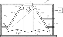
- the apparatus 600 may include a fan and a filter unit 640 , a set of cameras 601 , an array of LED (light emitting diodes) positioned on, or behind LED panels 602 , supporting bars 603 supporting the LED panels, a tool frame 605 to which the supporting bars 603 are attached. Further, the glass panel 1 may reside on edge defining elements S 1 and S 2 . Edge defining elements S 1 and S 2 may be attached to the tool frame 605 .
- the LED panels 602 may be configured to emit a beam of light towards a surface of the glass panel 1 . As illustrated in FIG. 6 , the LED panels 602 are arranged in a slanted manner, to include an opening at about a center for allowing flow of filtered air above the surface of the glass panel 1 . Further, the filtered air 641 may enter an enclosure defined by the tool frame 605 as indicated by an arrow pointing towards the glass panel 1 . Thus, the arrangement illustrated in FIG. 6 may allow the flow of filtered air applicable for clean-room applications.
- the cameras 601 may be configured to capture a reflected beam of light that includes at least a portion of the emitted beam as reflected from a surface of the glass plate 1 . Although two cameras 601 are shown in FIG. 1 , a single camera 601 may also be used in some of the embodiments of the present disclosure.
- the apparatus 600 may include a detector unit 606 configured to detect topography data of the substrate prior to a thin-film deposition and after the thin-film deposition on the substrate.
- the detector unit 606 may be configured to detect a change in optical path of the reflected beam of light to determine topography data of the substrate.
- the LED panel 602 may be used to direct the emitted beam to the surface of the glass panel 1 .
- the reflected emitted beam is distorted and thereby the reflected beam acquires an optical path difference or phase change associated with the curvature of the surface of the glass panel 1 , under measurement.
- the pinhole camera 601 may capture each point within the illuminated area on the surface of the glass panel. Thus, the curvature information at any point along any direction within the illuminated area can be obtained.
- FIG. 7 illustrates a flat glass panel 1 undergoing topography measurement by the apparatus 600 , illustrated in FIG. 6 .
- pinhole camera 601 receives a reflected beam.
- the reflected beam emanates from a point P on the flat glass panel 1 , the point P corresponds to LED A from the LED panel 602 which can otherwise be treated as emanating from a virtual image A′.
- the pinhole camera 601 is configured to capture the reflected beam, which is supposedly making an angle ⁇ with respect to an imaginary normal line corresponding to the pinhole camera.
- FIG. 8 illustrates a bent glass panel 1 undergoing topography measurement by the apparatus 600 , illustrated in FIG. 6 .
- pinhole camera 601 receives a reflected beam. Because the glass panel 1 is bent, the reflected beam emanates from a point Q on the surface of the bent glass panel which corresponds to LED A from the LED panel 602 . Similar to FIG. 7 the pinhole camera 601 is configured to capture the reflected beam which is supposedly making an angle ⁇ with respect to an imaginary normal line corresponding to the pinhole camera.
- FIG. 9 shows the reflected beams as emanating from the glass panel 1 when flat and when bent.
- the reflected beam emanates from a point P on the flat glass panel (which can otherwise be treated as emanating from a virtual image A′) and when the glass panel 1 is bent, the reflected beam emanates from a point Q on the bent glass panel (which can otherwise be treated as emanating from a virtual image A′′).
- the reflected beam makes an angle ⁇ when the reflection is from a flat glass panel and makes an angle different ⁇ ( ⁇ in this case) when the reflection is from a bent glass panel.
- a difference between the angles ⁇ and ⁇ may be used to derive a vertical displacement as undergone by the glass panel because of the thin-film deposition. For example, more is the vertical displacement; more will be the value of a difference between the angles ⁇ and ⁇ .
- angles ⁇ and ⁇ may be used to derive an extent of bend in the glass panel, which may be contributed for example by the radius of curvature as developed in the glass panel because of the stress developed in the thin-film deposited thereupon.
- more is the radius of curvature as developed in the glass panel more will be the value of a difference between the angles ⁇ and ⁇ .
- the detector 606 may detect the topography of the glass panel 1 based on the vertical displacement as derived from a difference between the angles ⁇ and ⁇ .
- FIG. 12 illustrates another arrangement of support of a bent glass panel 1 .
- the bent glass panel 1 is supported from below by two parallel rows R 1 and R 2 .
- the row R 1 may include a series of linearly placed edge defining elements S 1 .
- the row R 2 may include a series of linearly placed edge defining elements S 2 .
- the series of the edge defining elements S 1 from row R 1 and the series of edge defining elements S 2 from row R 2 may be positioned symmetrically with respect to an axis of the glass panel, similar to the positioning of edge defining elements S 1 and S 2 , as shown in FIG. 4 .
- the glass panel may be supported by several such rows R 1 and R 2 , each including a series of linearly placed edge defining elements and the several parallel rows being positioned symmetrically with respect to an axis of the glass panel.
- the support arrangement of the substrate as illustrated in FIG. 12 may help allow easier access of robot-end effectors to the substrate thus placed.
- the robot-end effectors may include effector prongs that can easily insert between the rows of linearly placed edge defining elements.
- an intrinsic stress of ⁇ 500 MPa (dashed line), 0 MPa (solid line) and +500 MPa (chain line) had developed at different prescribed points of the substrate having a vertical displacement as shown in FIGS.
- a graph illustrated in FIG. 13 illustrates the values of intrinsic stress developed in the thin-film deposited on the glass panel for different values of vertical displacement in the center region of the glass panel and regions near the edges of the glass panel.
- the graph as illustrated in FIG. 13 represents the values of intrinsic stress along the x-axis of the graph, assuming that the glass panel is positioned on a support arrangement as illustrated in FIG. 4 . Further, the graph represents the values for the vertical displacements of the glass panel along the y-axis of the graph.
- module or “component” may refer to specific hardware implementations configured to perform the actions of the module or component and/or software objects or software routines that may be stored on and/or executed by general purpose hardware (e.g., computer-readable media, processing devices, etc.) of the computing system.
- general purpose hardware e.g., computer-readable media, processing devices, etc.
- the different components, modules, engines, and services described in the present disclosure may be implemented as objects or processes that execute on the computing system (e.g., as separate threads). While some of the system and methods described in the present disclosure are generally described as being implemented in software (stored on and/or executed by general purpose hardware), specific hardware implementations or a combination of software and specific hardware implementations are also possible and contemplated.
- a “computing entity” may be any computing system as previously defined in the present disclosure, or any module or combination of modulates running on a computing system.
- any disjunctive word or phrase presenting two or more alternative terms, whether in the description, claims, or drawings, should be understood to contemplate the possibilities of including one of the terms, either of the terms, or both terms.
- the phrase “A or B” should be understood to include the possibilities of “A” or “B” or “A and B.”
Landscapes
- Physics & Mathematics (AREA)
- General Physics & Mathematics (AREA)
- Engineering & Computer Science (AREA)
- Manufacturing & Machinery (AREA)
- Computer Hardware Design (AREA)
- Microelectronics & Electronic Packaging (AREA)
- Power Engineering (AREA)
- Chemical & Material Sciences (AREA)
- Analytical Chemistry (AREA)
- Condensed Matter Physics & Semiconductors (AREA)
- Length Measuring Devices By Optical Means (AREA)
Abstract
Description
w 1(x)=(x−a)(x+a)(Q 2 x 2 +Q 0) for x≥0, x≤a (Equation 1)
w 2(x)=(x−a)(T 0 +T 1(x−a)1 +T 2(x−a)2 +T 3(x−a)3) for x≥a (Equation 2)
may be continuous at each point in general and at x=a in particular. The continuity of
at x=a implies:
T 0=2a(Q 2 a 2 +Q 0) (Equation 3)
where Plate=EY*h 3/(24(1−ν2)),
E gravity=Grav w(x) (Equation 5)
E=E elasticplate +E gravity +E film (Equation 7)
E TOT=2∫0 W/2 Edx (Equation 8)
E TOT=ƒ(Q 0 ,Q 2 ,T 1 ,T 2 ,T 3)
or
T 0 =R[+a([−(W 2−4Wa+2a 2+8K)/32])]
Claims (11)
Priority Applications (1)
| Application Number | Priority Date | Filing Date | Title |
|---|---|---|---|
| US16/741,628 US10964730B2 (en) | 2017-04-20 | 2020-01-13 | Non-contact measurement of a stress in a film on a substrate |
Applications Claiming Priority (3)
| Application Number | Priority Date | Filing Date | Title |
|---|---|---|---|
| US201762487857P | 2017-04-20 | 2017-04-20 | |
| US15/722,645 US10553623B2 (en) | 2017-04-20 | 2017-10-02 | Non-contact measurement of a stress in a film on a substrate |
| US16/741,628 US10964730B2 (en) | 2017-04-20 | 2020-01-13 | Non-contact measurement of a stress in a film on a substrate |
Related Parent Applications (1)
| Application Number | Title | Priority Date | Filing Date |
|---|---|---|---|
| US15/722,645 Division US10553623B2 (en) | 2017-04-20 | 2017-10-02 | Non-contact measurement of a stress in a film on a substrate |
Publications (2)
| Publication Number | Publication Date |
|---|---|
| US20200152783A1 US20200152783A1 (en) | 2020-05-14 |
| US10964730B2 true US10964730B2 (en) | 2021-03-30 |
Family
ID=63854161
Family Applications (2)
| Application Number | Title | Priority Date | Filing Date |
|---|---|---|---|
| US15/722,645 Active US10553623B2 (en) | 2017-04-20 | 2017-10-02 | Non-contact measurement of a stress in a film on a substrate |
| US16/741,628 Active US10964730B2 (en) | 2017-04-20 | 2020-01-13 | Non-contact measurement of a stress in a film on a substrate |
Family Applications Before (1)
| Application Number | Title | Priority Date | Filing Date |
|---|---|---|---|
| US15/722,645 Active US10553623B2 (en) | 2017-04-20 | 2017-10-02 | Non-contact measurement of a stress in a film on a substrate |
Country Status (1)
| Country | Link |
|---|---|
| US (2) | US10553623B2 (en) |
Families Citing this family (5)
| Publication number | Priority date | Publication date | Assignee | Title |
|---|---|---|---|---|
| KR102499831B1 (en) * | 2016-05-23 | 2023-02-14 | 코닝 인코포레이티드 | Method of predicting gravity-free shape of glass sheet and method of managing quality of a glass sheet based on gravity-free shape |
| CN109580058B (en) * | 2019-01-23 | 2021-03-09 | 福建省安元光学科技有限公司 | Method for judging stress of die product by utilizing surface roughness of coating |
| US11804410B2 (en) * | 2019-08-29 | 2023-10-31 | Taiwan Semiconductor Manufacturing Co., Ltd. | Thin-film non-uniform stress evaluation |
| WO2021096865A2 (en) * | 2019-11-12 | 2021-05-20 | Applied Materials, Inc. | Systems and methods for controlling non-uniformity |
| CN117393451B (en) * | 2023-12-07 | 2024-03-26 | 无锡卓海科技股份有限公司 | Method and system for measuring average curvature radius of wafer surface |
Citations (5)
| Publication number | Priority date | Publication date | Assignee | Title |
|---|---|---|---|---|
| US20030106378A1 (en) | 2001-05-25 | 2003-06-12 | Antonios Giannakopoulos | Determining large deformations and stresses of layered and graded structures to include effects of body forces |
| US20130068034A1 (en) * | 2010-06-02 | 2013-03-21 | Sigma Koki Co., Ltd. | Micromaterial strain measurement apparatus and method therefor techinical field |
| US20150226542A1 (en) | 2014-02-07 | 2015-08-13 | Luceo Co., Ltd. | Strain inspection apparatus |
| US20150276616A1 (en) | 2014-03-25 | 2015-10-01 | Kla-Tencor Corporation | Variable image field curvature for object inspection |
| US20180246006A1 (en) | 2017-02-27 | 2018-08-30 | Pile Dynamics, Inc. | Non-Contact Strain Measurement System And Method For Using The Same |
-
2017
- 2017-10-02 US US15/722,645 patent/US10553623B2/en active Active
-
2020
- 2020-01-13 US US16/741,628 patent/US10964730B2/en active Active
Patent Citations (5)
| Publication number | Priority date | Publication date | Assignee | Title |
|---|---|---|---|---|
| US20030106378A1 (en) | 2001-05-25 | 2003-06-12 | Antonios Giannakopoulos | Determining large deformations and stresses of layered and graded structures to include effects of body forces |
| US20130068034A1 (en) * | 2010-06-02 | 2013-03-21 | Sigma Koki Co., Ltd. | Micromaterial strain measurement apparatus and method therefor techinical field |
| US20150226542A1 (en) | 2014-02-07 | 2015-08-13 | Luceo Co., Ltd. | Strain inspection apparatus |
| US20150276616A1 (en) | 2014-03-25 | 2015-10-01 | Kla-Tencor Corporation | Variable image field curvature for object inspection |
| US20180246006A1 (en) | 2017-02-27 | 2018-08-30 | Pile Dynamics, Inc. | Non-Contact Strain Measurement System And Method For Using The Same |
Non-Patent Citations (1)
| Title |
|---|
| U.S. Appl. No. 15/722,645, filed Oct. 2, 2017. |
Also Published As
| Publication number | Publication date |
|---|---|
| US20200152783A1 (en) | 2020-05-14 |
| US10553623B2 (en) | 2020-02-04 |
| US20180308971A1 (en) | 2018-10-25 |
Similar Documents
| Publication | Publication Date | Title |
|---|---|---|
| US10964730B2 (en) | Non-contact measurement of a stress in a film on a substrate | |
| US6781702B2 (en) | Determining large deformations and stresses of layered and graded structures to include effects of body forces | |
| US9709473B2 (en) | Method and apparatus for measuring dynamic panel stiffness of outer panel for automobile parts | |
| CN104160241B (en) | Phase distribution analysis method, device and program of fringe image using high-dimensional luminance information | |
| TW201234516A (en) | Apparatus, device and method for determining alignment errors | |
| JP2010513925A (en) | A method for automatically and quantitatively analyzing the distortion of molded glass for vehicles using reflected optical images. | |
| WO2004013572A1 (en) | Curved shape inspection method and device | |
| CN107490428A (en) | Vibration visualization element, vibration measurement system and vibration measuring method | |
| JP4924426B2 (en) | Shape inspection method and apparatus | |
| US20150323313A1 (en) | Stress analysis of semiconductor wafers | |
| JPWO2019097578A1 (en) | Displacement component detection device, displacement component detection method, and program | |
| CN111735392A (en) | Flexible display panel and flattening degree test method thereof | |
| JP2003065755A (en) | Measuring method of displacement of tunnel shape | |
| CN110864649B (en) | A method for determining compensation value and determining flatness of optical module | |
| Slota et al. | The sensitivity of a photogrammetric method in formability analysis | |
| Djuzhev et al. | Non-destructive method of surface mapping to improve accuracy of mechanical stresses measurements | |
| US10718607B2 (en) | Determining geometric characteristics of reflective surfaces | |
| Toyoshi | Residual displacement and residual strain measurement for steel frame under seismic load by integrated dot centroid tracking method | |
| JP2516570B2 (en) | Reflector surface accuracy evaluation device for reflector antenna | |
| JP4848263B2 (en) | Plate member inspection device | |
| Iwasa | Experimental verification on simplified estimation method for envelope curve of wrinkled membrane surface distortions | |
| CN120352247B (en) | Testing method, device, equipment and storage medium for collaborative collection of material deformation | |
| JP5813524B2 (en) | Measuring device and method of measuring outer shape of reinforcing bar | |
| CN103471505B (en) | The detection method of via hole and pick-up unit | |
| WO2025245075A1 (en) | System and method for measuring oscillations and characterizing surface geometry of reflective surfaces by reflecting light onto an image capture screen |
Legal Events
| Date | Code | Title | Description |
|---|---|---|---|
| FEPP | Fee payment procedure |
Free format text: ENTITY STATUS SET TO UNDISCOUNTED (ORIGINAL EVENT CODE: BIG.); ENTITY STATUS OF PATENT OWNER: SMALL ENTITY |
|
| FEPP | Fee payment procedure |
Free format text: ENTITY STATUS SET TO SMALL (ORIGINAL EVENT CODE: SMAL); ENTITY STATUS OF PATENT OWNER: SMALL ENTITY |
|
| STPP | Information on status: patent application and granting procedure in general |
Free format text: NON FINAL ACTION MAILED |
|
| STPP | Information on status: patent application and granting procedure in general |
Free format text: PUBLICATIONS -- ISSUE FEE PAYMENT VERIFIED |
|
| STCF | Information on status: patent grant |
Free format text: PATENTED CASE |
|
| MAFP | Maintenance fee payment |
Free format text: PAYMENT OF MAINTENANCE FEE, 4TH YR, SMALL ENTITY (ORIGINAL EVENT CODE: M2551); ENTITY STATUS OF PATENT OWNER: SMALL ENTITY Year of fee payment: 4 |