US10962837B2 - Display device - Google Patents
Display device Download PDFInfo
- Publication number
- US10962837B2 US10962837B2 US15/808,247 US201715808247A US10962837B2 US 10962837 B2 US10962837 B2 US 10962837B2 US 201715808247 A US201715808247 A US 201715808247A US 10962837 B2 US10962837 B2 US 10962837B2
- Authority
- US
- United States
- Prior art keywords
- substrate
- color conversion
- disposed
- display panel
- layer
- Prior art date
- Legal status (The legal status is an assumption and is not a legal conclusion. Google has not performed a legal analysis and makes no representation as to the accuracy of the status listed.)
- Active
Links
Images


Classifications
-
- G—PHYSICS
- G02—OPTICS
- G02F—OPTICAL DEVICES OR ARRANGEMENTS FOR THE CONTROL OF LIGHT BY MODIFICATION OF THE OPTICAL PROPERTIES OF THE MEDIA OF THE ELEMENTS INVOLVED THEREIN; NON-LINEAR OPTICS; FREQUENCY-CHANGING OF LIGHT; OPTICAL LOGIC ELEMENTS; OPTICAL ANALOGUE/DIGITAL CONVERTERS
- G02F1/00—Devices or arrangements for the control of the intensity, colour, phase, polarisation or direction of light arriving from an independent light source, e.g. switching, gating or modulating; Non-linear optics
- G02F1/01—Devices or arrangements for the control of the intensity, colour, phase, polarisation or direction of light arriving from an independent light source, e.g. switching, gating or modulating; Non-linear optics for the control of the intensity, phase, polarisation or colour
- G02F1/13—Devices or arrangements for the control of the intensity, colour, phase, polarisation or direction of light arriving from an independent light source, e.g. switching, gating or modulating; Non-linear optics for the control of the intensity, phase, polarisation or colour based on liquid crystals, e.g. single liquid crystal display cells
- G02F1/133—Constructional arrangements; Operation of liquid crystal cells; Circuit arrangements
- G02F1/1333—Constructional arrangements; Manufacturing methods
- G02F1/1335—Structural association of cells with optical devices, e.g. polarisers or reflectors
- G02F1/133509—Filters, e.g. light shielding masks
- G02F1/133514—Colour filters
-
- G—PHYSICS
- G02—OPTICS
- G02F—OPTICAL DEVICES OR ARRANGEMENTS FOR THE CONTROL OF LIGHT BY MODIFICATION OF THE OPTICAL PROPERTIES OF THE MEDIA OF THE ELEMENTS INVOLVED THEREIN; NON-LINEAR OPTICS; FREQUENCY-CHANGING OF LIGHT; OPTICAL LOGIC ELEMENTS; OPTICAL ANALOGUE/DIGITAL CONVERTERS
- G02F1/00—Devices or arrangements for the control of the intensity, colour, phase, polarisation or direction of light arriving from an independent light source, e.g. switching, gating or modulating; Non-linear optics
- G02F1/01—Devices or arrangements for the control of the intensity, colour, phase, polarisation or direction of light arriving from an independent light source, e.g. switching, gating or modulating; Non-linear optics for the control of the intensity, phase, polarisation or colour
- G02F1/13—Devices or arrangements for the control of the intensity, colour, phase, polarisation or direction of light arriving from an independent light source, e.g. switching, gating or modulating; Non-linear optics for the control of the intensity, phase, polarisation or colour based on liquid crystals, e.g. single liquid crystal display cells
- G02F1/133—Constructional arrangements; Operation of liquid crystal cells; Circuit arrangements
- G02F1/1333—Constructional arrangements; Manufacturing methods
- G02F1/1335—Structural association of cells with optical devices, e.g. polarisers or reflectors
- G02F1/1336—Illuminating devices
- G02F1/133617—Illumination with ultraviolet light; Luminescent elements or materials associated to the cell
-
- G—PHYSICS
- G02—OPTICS
- G02F—OPTICAL DEVICES OR ARRANGEMENTS FOR THE CONTROL OF LIGHT BY MODIFICATION OF THE OPTICAL PROPERTIES OF THE MEDIA OF THE ELEMENTS INVOLVED THEREIN; NON-LINEAR OPTICS; FREQUENCY-CHANGING OF LIGHT; OPTICAL LOGIC ELEMENTS; OPTICAL ANALOGUE/DIGITAL CONVERTERS
- G02F1/00—Devices or arrangements for the control of the intensity, colour, phase, polarisation or direction of light arriving from an independent light source, e.g. switching, gating or modulating; Non-linear optics
- G02F1/01—Devices or arrangements for the control of the intensity, colour, phase, polarisation or direction of light arriving from an independent light source, e.g. switching, gating or modulating; Non-linear optics for the control of the intensity, phase, polarisation or colour
- G02F1/13—Devices or arrangements for the control of the intensity, colour, phase, polarisation or direction of light arriving from an independent light source, e.g. switching, gating or modulating; Non-linear optics for the control of the intensity, phase, polarisation or colour based on liquid crystals, e.g. single liquid crystal display cells
- G02F1/133—Constructional arrangements; Operation of liquid crystal cells; Circuit arrangements
- G02F1/1333—Constructional arrangements; Manufacturing methods
- G02F1/1335—Structural association of cells with optical devices, e.g. polarisers or reflectors
- G02F1/1336—Illuminating devices
- G02F1/133621—Illuminating devices providing coloured light
-
- G—PHYSICS
- G02—OPTICS
- G02F—OPTICAL DEVICES OR ARRANGEMENTS FOR THE CONTROL OF LIGHT BY MODIFICATION OF THE OPTICAL PROPERTIES OF THE MEDIA OF THE ELEMENTS INVOLVED THEREIN; NON-LINEAR OPTICS; FREQUENCY-CHANGING OF LIGHT; OPTICAL LOGIC ELEMENTS; OPTICAL ANALOGUE/DIGITAL CONVERTERS
- G02F1/00—Devices or arrangements for the control of the intensity, colour, phase, polarisation or direction of light arriving from an independent light source, e.g. switching, gating or modulating; Non-linear optics
- G02F1/01—Devices or arrangements for the control of the intensity, colour, phase, polarisation or direction of light arriving from an independent light source, e.g. switching, gating or modulating; Non-linear optics for the control of the intensity, phase, polarisation or colour
- G02F1/13—Devices or arrangements for the control of the intensity, colour, phase, polarisation or direction of light arriving from an independent light source, e.g. switching, gating or modulating; Non-linear optics for the control of the intensity, phase, polarisation or colour based on liquid crystals, e.g. single liquid crystal display cells
- G02F1/133—Constructional arrangements; Operation of liquid crystal cells; Circuit arrangements
- G02F1/1333—Constructional arrangements; Manufacturing methods
- G02F1/133305—Flexible substrates, e.g. plastics, organic film
-
- G—PHYSICS
- G02—OPTICS
- G02F—OPTICAL DEVICES OR ARRANGEMENTS FOR THE CONTROL OF LIGHT BY MODIFICATION OF THE OPTICAL PROPERTIES OF THE MEDIA OF THE ELEMENTS INVOLVED THEREIN; NON-LINEAR OPTICS; FREQUENCY-CHANGING OF LIGHT; OPTICAL LOGIC ELEMENTS; OPTICAL ANALOGUE/DIGITAL CONVERTERS
- G02F1/00—Devices or arrangements for the control of the intensity, colour, phase, polarisation or direction of light arriving from an independent light source, e.g. switching, gating or modulating; Non-linear optics
- G02F1/01—Devices or arrangements for the control of the intensity, colour, phase, polarisation or direction of light arriving from an independent light source, e.g. switching, gating or modulating; Non-linear optics for the control of the intensity, phase, polarisation or colour
- G02F1/13—Devices or arrangements for the control of the intensity, colour, phase, polarisation or direction of light arriving from an independent light source, e.g. switching, gating or modulating; Non-linear optics for the control of the intensity, phase, polarisation or colour based on liquid crystals, e.g. single liquid crystal display cells
- G02F1/133—Constructional arrangements; Operation of liquid crystal cells; Circuit arrangements
- G02F1/1333—Constructional arrangements; Manufacturing methods
- G02F1/1335—Structural association of cells with optical devices, e.g. polarisers or reflectors
- G02F1/133528—Polarisers
-
- G—PHYSICS
- G02—OPTICS
- G02F—OPTICAL DEVICES OR ARRANGEMENTS FOR THE CONTROL OF LIGHT BY MODIFICATION OF THE OPTICAL PROPERTIES OF THE MEDIA OF THE ELEMENTS INVOLVED THEREIN; NON-LINEAR OPTICS; FREQUENCY-CHANGING OF LIGHT; OPTICAL LOGIC ELEMENTS; OPTICAL ANALOGUE/DIGITAL CONVERTERS
- G02F1/00—Devices or arrangements for the control of the intensity, colour, phase, polarisation or direction of light arriving from an independent light source, e.g. switching, gating or modulating; Non-linear optics
- G02F1/01—Devices or arrangements for the control of the intensity, colour, phase, polarisation or direction of light arriving from an independent light source, e.g. switching, gating or modulating; Non-linear optics for the control of the intensity, phase, polarisation or colour
- G02F1/13—Devices or arrangements for the control of the intensity, colour, phase, polarisation or direction of light arriving from an independent light source, e.g. switching, gating or modulating; Non-linear optics for the control of the intensity, phase, polarisation or colour based on liquid crystals, e.g. single liquid crystal display cells
- G02F1/133—Constructional arrangements; Operation of liquid crystal cells; Circuit arrangements
- G02F1/136—Liquid crystal cells structurally associated with a semi-conducting layer or substrate, e.g. cells forming part of an integrated circuit
- G02F1/1362—Active matrix addressed cells
- G02F1/1368—Active matrix addressed cells in which the switching element is a three-electrode device
-
- H01L27/1218—
-
- H01L27/1222—
-
- H—ELECTRICITY
- H10—SEMICONDUCTOR DEVICES; ELECTRIC SOLID-STATE DEVICES NOT OTHERWISE PROVIDED FOR
- H10D—INORGANIC ELECTRIC SEMICONDUCTOR DEVICES
- H10D86/00—Integrated devices formed in or on insulating or conducting substrates, e.g. formed in silicon-on-insulator [SOI] substrates or on stainless steel or glass substrates
- H10D86/40—Integrated devices formed in or on insulating or conducting substrates, e.g. formed in silicon-on-insulator [SOI] substrates or on stainless steel or glass substrates characterised by multiple TFTs
- H10D86/411—Integrated devices formed in or on insulating or conducting substrates, e.g. formed in silicon-on-insulator [SOI] substrates or on stainless steel or glass substrates characterised by multiple TFTs characterised by materials, geometry or structure of the substrates
-
- H—ELECTRICITY
- H10—SEMICONDUCTOR DEVICES; ELECTRIC SOLID-STATE DEVICES NOT OTHERWISE PROVIDED FOR
- H10D—INORGANIC ELECTRIC SEMICONDUCTOR DEVICES
- H10D86/00—Integrated devices formed in or on insulating or conducting substrates, e.g. formed in silicon-on-insulator [SOI] substrates or on stainless steel or glass substrates
- H10D86/40—Integrated devices formed in or on insulating or conducting substrates, e.g. formed in silicon-on-insulator [SOI] substrates or on stainless steel or glass substrates characterised by multiple TFTs
- H10D86/421—Integrated devices formed in or on insulating or conducting substrates, e.g. formed in silicon-on-insulator [SOI] substrates or on stainless steel or glass substrates characterised by multiple TFTs having a particular composition, shape or crystalline structure of the active layer
-
- H—ELECTRICITY
- H10—SEMICONDUCTOR DEVICES; ELECTRIC SOLID-STATE DEVICES NOT OTHERWISE PROVIDED FOR
- H10D—INORGANIC ELECTRIC SEMICONDUCTOR DEVICES
- H10D86/00—Integrated devices formed in or on insulating or conducting substrates, e.g. formed in silicon-on-insulator [SOI] substrates or on stainless steel or glass substrates
- H10D86/40—Integrated devices formed in or on insulating or conducting substrates, e.g. formed in silicon-on-insulator [SOI] substrates or on stainless steel or glass substrates characterised by multiple TFTs
- H10D86/60—Integrated devices formed in or on insulating or conducting substrates, e.g. formed in silicon-on-insulator [SOI] substrates or on stainless steel or glass substrates characterised by multiple TFTs wherein the TFTs are in active matrices
-
- G—PHYSICS
- G02—OPTICS
- G02F—OPTICAL DEVICES OR ARRANGEMENTS FOR THE CONTROL OF LIGHT BY MODIFICATION OF THE OPTICAL PROPERTIES OF THE MEDIA OF THE ELEMENTS INVOLVED THEREIN; NON-LINEAR OPTICS; FREQUENCY-CHANGING OF LIGHT; OPTICAL LOGIC ELEMENTS; OPTICAL ANALOGUE/DIGITAL CONVERTERS
- G02F1/00—Devices or arrangements for the control of the intensity, colour, phase, polarisation or direction of light arriving from an independent light source, e.g. switching, gating or modulating; Non-linear optics
- G02F1/01—Devices or arrangements for the control of the intensity, colour, phase, polarisation or direction of light arriving from an independent light source, e.g. switching, gating or modulating; Non-linear optics for the control of the intensity, phase, polarisation or colour
- G02F1/13—Devices or arrangements for the control of the intensity, colour, phase, polarisation or direction of light arriving from an independent light source, e.g. switching, gating or modulating; Non-linear optics for the control of the intensity, phase, polarisation or colour based on liquid crystals, e.g. single liquid crystal display cells
- G02F1/133—Constructional arrangements; Operation of liquid crystal cells; Circuit arrangements
- G02F1/1333—Constructional arrangements; Manufacturing methods
- G02F1/133302—Rigid substrates, e.g. inorganic substrates
-
- G—PHYSICS
- G02—OPTICS
- G02F—OPTICAL DEVICES OR ARRANGEMENTS FOR THE CONTROL OF LIGHT BY MODIFICATION OF THE OPTICAL PROPERTIES OF THE MEDIA OF THE ELEMENTS INVOLVED THEREIN; NON-LINEAR OPTICS; FREQUENCY-CHANGING OF LIGHT; OPTICAL LOGIC ELEMENTS; OPTICAL ANALOGUE/DIGITAL CONVERTERS
- G02F1/00—Devices or arrangements for the control of the intensity, colour, phase, polarisation or direction of light arriving from an independent light source, e.g. switching, gating or modulating; Non-linear optics
- G02F1/01—Devices or arrangements for the control of the intensity, colour, phase, polarisation or direction of light arriving from an independent light source, e.g. switching, gating or modulating; Non-linear optics for the control of the intensity, phase, polarisation or colour
- G02F1/13—Devices or arrangements for the control of the intensity, colour, phase, polarisation or direction of light arriving from an independent light source, e.g. switching, gating or modulating; Non-linear optics for the control of the intensity, phase, polarisation or colour based on liquid crystals, e.g. single liquid crystal display cells
- G02F1/133—Constructional arrangements; Operation of liquid crystal cells; Circuit arrangements
- G02F1/1333—Constructional arrangements; Manufacturing methods
- G02F1/133368—Cells having two substrates with different characteristics, e.g. different thickness or material
-
- G—PHYSICS
- G02—OPTICS
- G02F—OPTICAL DEVICES OR ARRANGEMENTS FOR THE CONTROL OF LIGHT BY MODIFICATION OF THE OPTICAL PROPERTIES OF THE MEDIA OF THE ELEMENTS INVOLVED THEREIN; NON-LINEAR OPTICS; FREQUENCY-CHANGING OF LIGHT; OPTICAL LOGIC ELEMENTS; OPTICAL ANALOGUE/DIGITAL CONVERTERS
- G02F1/00—Devices or arrangements for the control of the intensity, colour, phase, polarisation or direction of light arriving from an independent light source, e.g. switching, gating or modulating; Non-linear optics
- G02F1/01—Devices or arrangements for the control of the intensity, colour, phase, polarisation or direction of light arriving from an independent light source, e.g. switching, gating or modulating; Non-linear optics for the control of the intensity, phase, polarisation or colour
- G02F1/13—Devices or arrangements for the control of the intensity, colour, phase, polarisation or direction of light arriving from an independent light source, e.g. switching, gating or modulating; Non-linear optics for the control of the intensity, phase, polarisation or colour based on liquid crystals, e.g. single liquid crystal display cells
- G02F1/133—Constructional arrangements; Operation of liquid crystal cells; Circuit arrangements
- G02F1/1333—Constructional arrangements; Manufacturing methods
- G02F1/1335—Structural association of cells with optical devices, e.g. polarisers or reflectors
- G02F1/133509—Filters, e.g. light shielding masks
- G02F1/133514—Colour filters
- G02F1/133519—Overcoatings
-
- G—PHYSICS
- G02—OPTICS
- G02F—OPTICAL DEVICES OR ARRANGEMENTS FOR THE CONTROL OF LIGHT BY MODIFICATION OF THE OPTICAL PROPERTIES OF THE MEDIA OF THE ELEMENTS INVOLVED THEREIN; NON-LINEAR OPTICS; FREQUENCY-CHANGING OF LIGHT; OPTICAL LOGIC ELEMENTS; OPTICAL ANALOGUE/DIGITAL CONVERTERS
- G02F1/00—Devices or arrangements for the control of the intensity, colour, phase, polarisation or direction of light arriving from an independent light source, e.g. switching, gating or modulating; Non-linear optics
- G02F1/01—Devices or arrangements for the control of the intensity, colour, phase, polarisation or direction of light arriving from an independent light source, e.g. switching, gating or modulating; Non-linear optics for the control of the intensity, phase, polarisation or colour
- G02F1/13—Devices or arrangements for the control of the intensity, colour, phase, polarisation or direction of light arriving from an independent light source, e.g. switching, gating or modulating; Non-linear optics for the control of the intensity, phase, polarisation or colour based on liquid crystals, e.g. single liquid crystal display cells
- G02F1/133—Constructional arrangements; Operation of liquid crystal cells; Circuit arrangements
- G02F1/1333—Constructional arrangements; Manufacturing methods
- G02F1/1335—Structural association of cells with optical devices, e.g. polarisers or reflectors
- G02F1/1336—Illuminating devices
- G02F1/133614—Illuminating devices using photoluminescence, e.g. phosphors illuminated by UV or blue light
-
- G—PHYSICS
- G02—OPTICS
- G02F—OPTICAL DEVICES OR ARRANGEMENTS FOR THE CONTROL OF LIGHT BY MODIFICATION OF THE OPTICAL PROPERTIES OF THE MEDIA OF THE ELEMENTS INVOLVED THEREIN; NON-LINEAR OPTICS; FREQUENCY-CHANGING OF LIGHT; OPTICAL LOGIC ELEMENTS; OPTICAL ANALOGUE/DIGITAL CONVERTERS
- G02F1/00—Devices or arrangements for the control of the intensity, colour, phase, polarisation or direction of light arriving from an independent light source, e.g. switching, gating or modulating; Non-linear optics
- G02F1/01—Devices or arrangements for the control of the intensity, colour, phase, polarisation or direction of light arriving from an independent light source, e.g. switching, gating or modulating; Non-linear optics for the control of the intensity, phase, polarisation or colour
- G02F1/13—Devices or arrangements for the control of the intensity, colour, phase, polarisation or direction of light arriving from an independent light source, e.g. switching, gating or modulating; Non-linear optics for the control of the intensity, phase, polarisation or colour based on liquid crystals, e.g. single liquid crystal display cells
- G02F1/133—Constructional arrangements; Operation of liquid crystal cells; Circuit arrangements
- G02F1/1333—Constructional arrangements; Manufacturing methods
- G02F1/1335—Structural association of cells with optical devices, e.g. polarisers or reflectors
- G02F1/1336—Illuminating devices
- G02F1/133624—Illuminating devices characterised by their spectral emissions
-
- G02F2001/133302—
-
- G02F2001/133368—
-
- G02F2001/133519—
-
- G02F2001/133614—
-
- G—PHYSICS
- G02—OPTICS
- G02F—OPTICAL DEVICES OR ARRANGEMENTS FOR THE CONTROL OF LIGHT BY MODIFICATION OF THE OPTICAL PROPERTIES OF THE MEDIA OF THE ELEMENTS INVOLVED THEREIN; NON-LINEAR OPTICS; FREQUENCY-CHANGING OF LIGHT; OPTICAL LOGIC ELEMENTS; OPTICAL ANALOGUE/DIGITAL CONVERTERS
- G02F2201/00—Constructional arrangements not provided for in groups G02F1/00 - G02F7/00
- G02F2201/12—Constructional arrangements not provided for in groups G02F1/00 - G02F7/00 electrode
- G02F2201/123—Constructional arrangements not provided for in groups G02F1/00 - G02F7/00 electrode pixel
-
- G—PHYSICS
- G02—OPTICS
- G02F—OPTICAL DEVICES OR ARRANGEMENTS FOR THE CONTROL OF LIGHT BY MODIFICATION OF THE OPTICAL PROPERTIES OF THE MEDIA OF THE ELEMENTS INVOLVED THEREIN; NON-LINEAR OPTICS; FREQUENCY-CHANGING OF LIGHT; OPTICAL LOGIC ELEMENTS; OPTICAL ANALOGUE/DIGITAL CONVERTERS
- G02F2201/00—Constructional arrangements not provided for in groups G02F1/00 - G02F7/00
- G02F2201/56—Substrates having a particular shape, e.g. non-rectangular
-
- G—PHYSICS
- G02—OPTICS
- G02F—OPTICAL DEVICES OR ARRANGEMENTS FOR THE CONTROL OF LIGHT BY MODIFICATION OF THE OPTICAL PROPERTIES OF THE MEDIA OF THE ELEMENTS INVOLVED THEREIN; NON-LINEAR OPTICS; FREQUENCY-CHANGING OF LIGHT; OPTICAL LOGIC ELEMENTS; OPTICAL ANALOGUE/DIGITAL CONVERTERS
- G02F2202/00—Materials and properties
- G02F2202/36—Micro- or nanomaterials
Definitions
- the present inventive concept provides a display device improved with improved color reproducibility and having a thin thickness. Also, a curved display device is provided.
- One of the first substrate and the second substrate disposed close to the color conversion panel may have a thickness less than that of the other substrate disposed far away from the color conversion panel.
- the first display panel may be disposed between the liquid crystal layer and the color conversion panel.
- a light unit disposed at a rear surface of the display panel, a first polarizer disposed between the display panel and the color conversion panel, and a second polarizer disposed between the display panel and the light unit may be further included.
- a light unit disposed at a rear surface of the display panel, a first polarizer disposed between the first substrate and the liquid crystal layer, and a second polarizer disposed between the display panel and the light unit may be further included.
- the display device may be a curved display device.
- the second substrate may be disposed between the color conversion panel and the liquid crystal layer, and the second substrate may be one of a glass substrate and a plastic substrate.
- the thickness of the glass substrate may be greater than about 0.03 mm and less than about 0.07 mm.
- a display device includes: a color conversion panel; and a display panel overlapping the color conversion panel, wherein the color conversion panel includes a color conversion layer including a nano-crystalline semiconductor and a transmission layer, the display panel includes a first display panel including a first substrate and a thin film transistor disposed on the first substrate, a second display panel including a second substrate and overlapping the first display panel, and a liquid crystal layer disposed between the first display panel and the second display panel, and the first display panel is disposed between the liquid crystal layer and the color conversion panel.
- a display device includes a color conversion panel; and a display panel overlapping the color conversion panel, wherein the color conversion panel includes a color conversion layer including a nano-crystalline semiconductor and a transmission layer, the display panel includes a first substrate where on which a thin film transistor is located, and a thin film encapsulation layer overlapping the first substrate, wherein the thickness of one of the first substrate and the thin film encapsulation layer disposed close to the color conversion panel is about 0.07 mm or less.
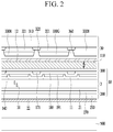
- FIG. 5 is a top plan view of a display device according to an exemplary embodiment of the present inventive concept.
- a thickness of the first substrate 110 is thin, a length of a path of the light passing through the liquid crystal layer 3 , the first display panel 100 and the color conversion panel 30 may be reduced.
- the present specification describes an exemplary embodiment in which the blue light cutting filter 321 disposed at the region emitting the red light and the blue light cutting filter 321 disposed at the region emitting the green light are separated.
- the blue light cutting filter 321 disposed at the region emitting the red light and the blue light cutting filter 321 positioned at the region emitting the green light may be connected to each other.
- the blue light cutting filter 321 may have an opening overlapping the transmission layer 330 B.
- the green phosphor may contain one of yttrium aluminum garnet (YAG), (Ca, Sr, Ba)2SiO4, SrGa2S4, BAM, ⁇ -SiAlON, ⁇ -SiAlON, Ca3Sc2Si3O12, Tb3Al5O12, BaSiO4, CaAlSiON, and (Sr(1-x)Bax)Si2O2N2, but the present disclosure is not limited thereto.
- the green color conversion layer 330 G may include at least one kind of green phosphor. In this case, the x may be any number between 0 and 1.
- the Group III-V compound may be selected from a two-element compound selected from GaN, GaP, GaAs, GaSb, AlN, AlP, AlAs, AlSb, InN, InP, InAs, InSb, and a mixture thereof, a three-element compound selected from GaNP, GaNAs, GaNSb, GaPAs, GaPSb, AlNP, AlNAs, AlNSb, AlPAs, AlPSb, InNP, InNAs, InNSb, InPAs, InPSb, and a mixture thereof, and a four-element compound selected from GaAlNAs, GaAlNSb, GaAlPAs, GaAlPSb, GaInNP, GaInNAs, GaInNSb, GaInPAs, GaInPSb, GaAlNP, InAlNP, InAlNAs, InAlNSb, InAlPAs, InAlPSb, and a mixture thereof.
- the quantum dots may have a full width at half maximum (FWHM) of a light-emitting wavelength spectrum of about 45 nm or less, preferably about 40 nm or less, and more preferably about 30 nm or less, such that the color purity and the color reproducibility may be improved. Also, the light emitted through these quantum dots is emitted in all directions, thereby the light viewing angle may be improved.
- FWHM full width at half maximum
- the above-described light blocking member 320 , red color conversion layer 330 R, green color conversion layer 330 G, and transmission layer 330 B may include a photosensitive resin as one example, and may be formed by a photolithography process. Also, they may be formed through a printing process. In this case, the light blocking member 320 , the red color conversion layer 330 R, the green color conversion layer 330 G, and the transmission layer 330 B may be another material other than the photosensitive resin.
- the present specification describes the color conversion layer, the transmission layer, and the light blocking member that are formed by the photolithography process or the printing process, however it is not limited thereto.
- the display device may be a curved display device that is curved in one direction.
- the first display panel 100 which includes the pixel electrode 191 may be attached to the color conversion panel 30 .
- a misalignment between the color conversion panel 30 and the first display panel 100 may be prevented and color mixture may be controlled.
- the first substrate 110 disposed adjacent to the color conversion panel 30 is thin, a light path toward the color conversion panel 30 through the liquid crystal layer 3 may also be shortened. Accordingly, the color mixture between the color conversion layer and the transmission layer adjacent to each other may be prevented.
- the second display panel 200 is disposed between the liquid crystal layer 3 and the light unit 500 .
- the second substrate 210 included in the second display panel 200 overlaps and is separated from the first substrate 110 .
- the common electrode 270 may be disposed between the second substrate 210 and the liquid crystal layer 3
- the second alignment layer 21 may be disposed between the common electrode 270 and the liquid crystal layer 3 .
- the display panel 10 includes a first display panel 100 , a second display panel 200 overlapping the first display panel 100 , and a liquid crystal layer 3 disposed between the first display panel 100 and the second display panel 200 .
- the first display panel 100 may be disposed between the light unit 500 and the liquid crystal layer 3
- the second display panel 200 may be disposed between the color conversion panel 30 and the liquid crystal layer 3 .
- the second substrate 210 may be the glass substrate or the plastic substrate.
- the thickness t of the first substrate 110 may be greater than about 0.03 mm and less than about 0.07 mm.
- the second substrate 210 may be provided by etching the glass substrate having a thicker thickness than the above-described range, or by providing the glass substrate itself having a thickness of the above-described range.
- the common electrode 270 may be disposed between the second substrate 210 and the liquid crystal layer 3
- the second alignment layer 21 may be disposed between the common electrode 270 and the liquid crystal layer 3 .
- Ohmic contacts 163 and 165 are disposed on the first semiconductor layer 154 a and the second semiconductor layer 154 b .
- the ohmic contacts may be omitted depending on an exemplary embodiment.
- the first drain electrode 175 a and the second drain electrode 175 b are separated from each other and are separated from the data line 171 and the driving voltage line 172 .
- a passivation layer 180 is disposed on the data conductors 171 , 172 , 173 a , 173 b , 175 a , and 175 b and the exposed semiconductor layers 154 a and 154 b.
- Contact holes 185 a and 185 b for respectively exposing the first drain electrode 175 a and the second drain electrode 175 b are positioned in the passivation layer 180
- a contact hole 184 for exposing the second gate electrode 124 b is positioned in the passivation layer 180 and the gate insulating layer 140 .
- a pixel electrode 191 and a connecting member 85 are disposed on the passivation layer 180 .
- the pixel electrode 191 is physically and electrically connected to the second drain electrode 175 b through the contact hole 185 b
- the connecting member 85 is connected with the second gate electrode 124 b and the first drain electrode 175 a through the contact holes 184 and 185 a.
- the first gate electrode 124 a connected to the gate line 121 , the first source electrode 173 a connected to the data line 171 , and the first drain electrode 175 a form a switching thin film transistor (TFT) Qs along with the first semiconductor layer 154 a , and the channel of the switching thin film transistor Qs is formed in the first semiconductor layer 154 a between the first source electrode 173 a and the first drain electrode 175 a.
- TFT switching thin film transistor
- This emissive display device may emit the light upward and downward with respect to the first substrate 110 to display the image, and the exemplary embodiment in which the light is emitted upward with respect to the first substrate 110 is described according to an exemplary embodiment of the present invention.
- the present disclosure has described an embodiment in which the thin film encapsulation layer 400 is adjacent to the color conversion panel 30 and the first substrate 110 is spaced from the color conversion panel 30 , it is also possible that the first substrate 110 is adjacent to the color conversion panel 30 and the thin film encapsulation layer 400 is spaced from the color conversion panel 30 as shown in FIG. 7 .
- the description of the thin film encapsulation layer 400 described with reference to FIGS. 5 and 6 can be applied to the first substrate 110 .
Landscapes
- Physics & Mathematics (AREA)
- Nonlinear Science (AREA)
- Chemical & Material Sciences (AREA)
- Crystallography & Structural Chemistry (AREA)
- Mathematical Physics (AREA)
- General Physics & Mathematics (AREA)
- Optics & Photonics (AREA)
- Engineering & Computer Science (AREA)
- Microelectronics & Electronic Packaging (AREA)
- Liquid Crystal (AREA)
- Devices For Indicating Variable Information By Combining Individual Elements (AREA)
Abstract
Description
Claims (19)
Priority Applications (1)
| Application Number | Priority Date | Filing Date | Title |
|---|---|---|---|
| US17/191,754 US11243435B2 (en) | 2016-11-18 | 2021-03-04 | Display device |
Applications Claiming Priority (2)
| Application Number | Priority Date | Filing Date | Title |
|---|---|---|---|
| KR10-2016-0153903 | 2016-11-18 | ||
| KR1020160153903A KR102730912B1 (en) | 2016-11-18 | 2016-11-18 | Display device |
Related Child Applications (1)
| Application Number | Title | Priority Date | Filing Date |
|---|---|---|---|
| US17/191,754 Continuation US11243435B2 (en) | 2016-11-18 | 2021-03-04 | Display device |
Publications (2)
| Publication Number | Publication Date |
|---|---|
| US20180143497A1 US20180143497A1 (en) | 2018-05-24 |
| US10962837B2 true US10962837B2 (en) | 2021-03-30 |
Family
ID=62147611
Family Applications (2)
| Application Number | Title | Priority Date | Filing Date |
|---|---|---|---|
| US15/808,247 Active US10962837B2 (en) | 2016-11-18 | 2017-11-09 | Display device |
| US17/191,754 Active US11243435B2 (en) | 2016-11-18 | 2021-03-04 | Display device |
Family Applications After (1)
| Application Number | Title | Priority Date | Filing Date |
|---|---|---|---|
| US17/191,754 Active US11243435B2 (en) | 2016-11-18 | 2021-03-04 | Display device |
Country Status (3)
| Country | Link |
|---|---|
| US (2) | US10962837B2 (en) |
| KR (1) | KR102730912B1 (en) |
| CN (1) | CN108072993A (en) |
Families Citing this family (9)
| Publication number | Priority date | Publication date | Assignee | Title |
|---|---|---|---|---|
| KR102521100B1 (en) * | 2018-01-08 | 2023-04-14 | 삼성디스플레이 주식회사 | Display device |
| CN108628038B (en) * | 2018-06-28 | 2021-02-26 | 京东方科技集团股份有限公司 | Light-emitting transistor and light-emitting method thereof, array substrate and display device |
| KR102333769B1 (en) * | 2018-06-29 | 2021-12-01 | 삼성디스플레이 주식회사 | Display device |
| TWI698678B (en) * | 2019-04-09 | 2020-07-11 | 友達光電股份有限公司 | Display device |
| KR20210142031A (en) * | 2020-05-14 | 2021-11-24 | 삼성디스플레이 주식회사 | Display apparatus |
| US12197080B2 (en) | 2020-06-30 | 2025-01-14 | Harman International Industries, Incorporated | Vehicle quantum dot display system and method |
| KR102845502B1 (en) * | 2020-07-14 | 2025-08-13 | 삼성디스플레이 주식회사 | Display panel |
| KR20220072959A (en) | 2020-11-25 | 2022-06-03 | 삼성디스플레이 주식회사 | Display apparatus |
| CN112670326A (en) * | 2020-12-23 | 2021-04-16 | 武汉华星光电半导体显示技术有限公司 | Display panel and display device |
Citations (9)
| Publication number | Priority date | Publication date | Assignee | Title |
|---|---|---|---|---|
| US20050140839A1 (en) * | 2003-12-30 | 2005-06-30 | Hyung Ki Hong | Liquid crystal display device |
| US20070165170A1 (en) * | 2005-12-26 | 2007-07-19 | Koichi Fukuda | Liquid crystal display and display |
| US20130242228A1 (en) * | 2012-03-15 | 2013-09-19 | Samsung Display Co., Ltd. | Liquid crystal display and manufacturing method thereof |
| US20140043566A1 (en) * | 2012-08-09 | 2014-02-13 | Samsung Display Co., Ltd. | Display device with increased optical efficiency |
| US20140192294A1 (en) * | 2013-01-07 | 2014-07-10 | Innolux Corporation | Patterned color conversion film and display device using the same |
| US20150198844A1 (en) * | 2014-01-10 | 2015-07-16 | Apple Inc. | Display with Column Spacer Structures |
| US20150286097A1 (en) * | 2014-04-03 | 2015-10-08 | Samsung Display Co., Ltd. | Display device including a color conversion layer |
| US20150378193A1 (en) * | 2014-06-30 | 2015-12-31 | Samsung Display Co., Ltd. | Curved display device and method of manufacturing the same |
| US20160231615A1 (en) | 2015-02-06 | 2016-08-11 | Samsung Display Co., Ltd. | Photosensitive resin composition and a display panel including the same |
Family Cites Families (13)
| Publication number | Priority date | Publication date | Assignee | Title |
|---|---|---|---|---|
| JP2007025621A (en) | 2005-06-15 | 2007-02-01 | Seiko Instruments Inc | Color display unit |
| CN1881034A (en) * | 2005-06-15 | 2006-12-20 | 精工电子有限公司 | Color display unit |
| JP2008107510A (en) | 2006-10-25 | 2008-05-08 | Nitto Denko Corp | Display element substrate and manufacturing method thereof |
| JP2009134275A (en) * | 2007-11-02 | 2009-06-18 | Sony Corp | Color liquid crystal display device assembly and light conversion device |
| CN101680968A (en) * | 2008-03-21 | 2010-03-24 | 木本股份有限公司 | Optical film, laminate, and touch panel |
| KR20100037283A (en) * | 2008-10-01 | 2010-04-09 | 삼성전자주식회사 | Liquid crystal display and manufacturing method of the same |
| EP2410374A1 (en) | 2009-03-19 | 2012-01-25 | Sharp Kabushiki Kaisha | Display panel and display device |
| JP5706271B2 (en) | 2011-08-24 | 2015-04-22 | 日東電工株式会社 | Method for producing transparent conductive film |
| KR20150028608A (en) * | 2013-09-06 | 2015-03-16 | 삼성디스플레이 주식회사 | Display panel |
| DE102014227002A1 (en) * | 2014-01-10 | 2015-07-16 | Apple Inc. | Display with column spacer structures |
| KR102174381B1 (en) * | 2014-04-03 | 2020-11-05 | 삼성디스플레이 주식회사 | Display device |
| KR102239112B1 (en) * | 2014-07-30 | 2021-04-13 | 삼성디스플레이 주식회사 | Display device |
| KR102243483B1 (en) * | 2014-11-11 | 2021-04-22 | 삼성디스플레이 주식회사 | Display |
-
2016
- 2016-11-18 KR KR1020160153903A patent/KR102730912B1/en active Active
-
2017
- 2017-11-09 US US15/808,247 patent/US10962837B2/en active Active
- 2017-11-16 CN CN201711137475.5A patent/CN108072993A/en active Pending
-
2021
- 2021-03-04 US US17/191,754 patent/US11243435B2/en active Active
Patent Citations (9)
| Publication number | Priority date | Publication date | Assignee | Title |
|---|---|---|---|---|
| US20050140839A1 (en) * | 2003-12-30 | 2005-06-30 | Hyung Ki Hong | Liquid crystal display device |
| US20070165170A1 (en) * | 2005-12-26 | 2007-07-19 | Koichi Fukuda | Liquid crystal display and display |
| US20130242228A1 (en) * | 2012-03-15 | 2013-09-19 | Samsung Display Co., Ltd. | Liquid crystal display and manufacturing method thereof |
| US20140043566A1 (en) * | 2012-08-09 | 2014-02-13 | Samsung Display Co., Ltd. | Display device with increased optical efficiency |
| US20140192294A1 (en) * | 2013-01-07 | 2014-07-10 | Innolux Corporation | Patterned color conversion film and display device using the same |
| US20150198844A1 (en) * | 2014-01-10 | 2015-07-16 | Apple Inc. | Display with Column Spacer Structures |
| US20150286097A1 (en) * | 2014-04-03 | 2015-10-08 | Samsung Display Co., Ltd. | Display device including a color conversion layer |
| US20150378193A1 (en) * | 2014-06-30 | 2015-12-31 | Samsung Display Co., Ltd. | Curved display device and method of manufacturing the same |
| US20160231615A1 (en) | 2015-02-06 | 2016-08-11 | Samsung Display Co., Ltd. | Photosensitive resin composition and a display panel including the same |
Also Published As
| Publication number | Publication date |
|---|---|
| KR20180056443A (en) | 2018-05-29 |
| KR102730912B1 (en) | 2024-11-15 |
| US11243435B2 (en) | 2022-02-08 |
| CN108072993A (en) | 2018-05-25 |
| US20180143497A1 (en) | 2018-05-24 |
| US20210191199A1 (en) | 2021-06-24 |
Similar Documents
| Publication | Publication Date | Title |
|---|---|---|
| US11187942B2 (en) | Color conversion panel and display device including the same | |
| US12353091B2 (en) | Display device having improved light emission and color reproducibility | |
| US11608944B2 (en) | Color conversion panel and display device including color conversion panel | |
| US11243435B2 (en) | Display device | |
| US9989806B2 (en) | Color conversion panel and display device including the same | |
| US11048029B2 (en) | Color conversion panel, manufacturing method of the same, and display device including the same | |
| US9952740B1 (en) | Color conversion panel, display device including the same, and method of manufacturing color conversion panel | |
| US11073718B2 (en) | Color conversion panel having blue light cutting filter and display device including the same | |
| US10379395B2 (en) | Color conversion panel and display device including the same | |
| US20180314107A1 (en) | Color conversion panel and display device including the same | |
| CN109001932A (en) | Show equipment | |
| US11067844B2 (en) | Color conversion panel and display device including the same | |
| US20190064600A1 (en) | Color conversion display panel and display device including the same |
Legal Events
| Date | Code | Title | Description |
|---|---|---|---|
| FEPP | Fee payment procedure |
Free format text: ENTITY STATUS SET TO UNDISCOUNTED (ORIGINAL EVENT CODE: BIG.); ENTITY STATUS OF PATENT OWNER: LARGE ENTITY |
|
| AS | Assignment |
Owner name: SAMSUNG DISPLAY CO., LTD., KOREA, REPUBLIC OF Free format text: ASSIGNMENT OF ASSIGNORS INTEREST;ASSIGNORS:KIM, DUK-SUNG;KWON, JUNG HYUN;KIM, DONG-YOON;REEL/FRAME:044104/0473 Effective date: 20170414 |
|
| STPP | Information on status: patent application and granting procedure in general |
Free format text: RESPONSE TO NON-FINAL OFFICE ACTION ENTERED AND FORWARDED TO EXAMINER |
|
| STPP | Information on status: patent application and granting procedure in general |
Free format text: FINAL REJECTION MAILED |
|
| STPP | Information on status: patent application and granting procedure in general |
Free format text: DOCKETED NEW CASE - READY FOR EXAMINATION |
|
| STPP | Information on status: patent application and granting procedure in general |
Free format text: NON FINAL ACTION MAILED |
|
| STPP | Information on status: patent application and granting procedure in general |
Free format text: FINAL REJECTION MAILED |
|
| STPP | Information on status: patent application and granting procedure in general |
Free format text: ADVISORY ACTION MAILED |
|
| STPP | Information on status: patent application and granting procedure in general |
Free format text: DOCKETED NEW CASE - READY FOR EXAMINATION |
|
| STPP | Information on status: patent application and granting procedure in general |
Free format text: PUBLICATIONS -- ISSUE FEE PAYMENT VERIFIED |
|
| STCF | Information on status: patent grant |
Free format text: PATENTED CASE |
|
| MAFP | Maintenance fee payment |
Free format text: PAYMENT OF MAINTENANCE FEE, 4TH YEAR, LARGE ENTITY (ORIGINAL EVENT CODE: M1551); ENTITY STATUS OF PATENT OWNER: LARGE ENTITY Year of fee payment: 4 |