US10951115B2 - Switching regulator - Google Patents
Switching regulator Download PDFInfo
- Publication number
- US10951115B2 US10951115B2 US16/255,319 US201916255319A US10951115B2 US 10951115 B2 US10951115 B2 US 10951115B2 US 201916255319 A US201916255319 A US 201916255319A US 10951115 B2 US10951115 B2 US 10951115B2
- Authority
- US
- United States
- Prior art keywords
- voltage
- output
- current
- switching regulator
- generation circuit
- Prior art date
- Legal status (The legal status is an assumption and is not a legal conclusion. Google has not performed a legal analysis and makes no representation as to the accuracy of the status listed.)
- Active, expires
Links
- 230000007274 generation of a signal involved in cell-cell signaling Effects 0.000 claims abstract description 18
- 239000003990 capacitor Substances 0.000 claims description 23
- 238000010586 diagram Methods 0.000 description 22
- 230000000630 rising effect Effects 0.000 description 12
- 238000000034 method Methods 0.000 description 7
- 238000001514 detection method Methods 0.000 description 5
- 230000001052 transient effect Effects 0.000 description 5
- 230000009467 reduction Effects 0.000 description 4
- 230000008901 benefit Effects 0.000 description 3
- 230000008859 change Effects 0.000 description 3
- 238000003708 edge detection Methods 0.000 description 3
- 239000000446 fuel Substances 0.000 description 3
- 238000012986 modification Methods 0.000 description 3
- 230000004048 modification Effects 0.000 description 3
- 230000004044 response Effects 0.000 description 3
- 230000006641 stabilisation Effects 0.000 description 3
- 238000011105 stabilization Methods 0.000 description 3
- 230000015556 catabolic process Effects 0.000 description 2
- 244000145845 chattering Species 0.000 description 2
- 230000000694 effects Effects 0.000 description 2
- 230000004043 responsiveness Effects 0.000 description 2
- 239000004065 semiconductor Substances 0.000 description 2
- 230000003466 anti-cipated effect Effects 0.000 description 1
- 238000005516 engineering process Methods 0.000 description 1
- 230000010354 integration Effects 0.000 description 1
- 239000000463 material Substances 0.000 description 1
- 230000003071 parasitic effect Effects 0.000 description 1
- 230000008569 process Effects 0.000 description 1
- 238000010992 reflux Methods 0.000 description 1
- 230000000087 stabilizing effect Effects 0.000 description 1
- 230000001629 suppression Effects 0.000 description 1
Images


Classifications
-
- H—ELECTRICITY
- H02—GENERATION; CONVERSION OR DISTRIBUTION OF ELECTRIC POWER
- H02M—APPARATUS FOR CONVERSION BETWEEN AC AND AC, BETWEEN AC AND DC, OR BETWEEN DC AND DC, AND FOR USE WITH MAINS OR SIMILAR POWER SUPPLY SYSTEMS; CONVERSION OF DC OR AC INPUT POWER INTO SURGE OUTPUT POWER; CONTROL OR REGULATION THEREOF
- H02M3/00—Conversion of DC power input into DC power output
- H02M3/02—Conversion of DC power input into DC power output without intermediate conversion into AC
- H02M3/04—Conversion of DC power input into DC power output without intermediate conversion into AC by static converters
- H02M3/10—Conversion of DC power input into DC power output without intermediate conversion into AC by static converters using discharge tubes with control electrode or semiconductor devices with control electrode
- H02M3/145—Conversion of DC power input into DC power output without intermediate conversion into AC by static converters using discharge tubes with control electrode or semiconductor devices with control electrode using devices of a triode or transistor type requiring continuous application of a control signal
- H02M3/155—Conversion of DC power input into DC power output without intermediate conversion into AC by static converters using discharge tubes with control electrode or semiconductor devices with control electrode using devices of a triode or transistor type requiring continuous application of a control signal using semiconductor devices only
-
- H—ELECTRICITY
- H02—GENERATION; CONVERSION OR DISTRIBUTION OF ELECTRIC POWER
- H02M—APPARATUS FOR CONVERSION BETWEEN AC AND AC, BETWEEN AC AND DC, OR BETWEEN DC AND DC, AND FOR USE WITH MAINS OR SIMILAR POWER SUPPLY SYSTEMS; CONVERSION OF DC OR AC INPUT POWER INTO SURGE OUTPUT POWER; CONTROL OR REGULATION THEREOF
- H02M1/00—Details of apparatus for conversion
- H02M1/14—Arrangements for reducing ripples from DC input or output
-
- H—ELECTRICITY
- H02—GENERATION; CONVERSION OR DISTRIBUTION OF ELECTRIC POWER
- H02M—APPARATUS FOR CONVERSION BETWEEN AC AND AC, BETWEEN AC AND DC, OR BETWEEN DC AND DC, AND FOR USE WITH MAINS OR SIMILAR POWER SUPPLY SYSTEMS; CONVERSION OF DC OR AC INPUT POWER INTO SURGE OUTPUT POWER; CONTROL OR REGULATION THEREOF
- H02M1/00—Details of apparatus for conversion
- H02M1/08—Circuits specially adapted for the generation of control voltages for semiconductor devices incorporated in static converters
-
- H—ELECTRICITY
- H02—GENERATION; CONVERSION OR DISTRIBUTION OF ELECTRIC POWER
- H02M—APPARATUS FOR CONVERSION BETWEEN AC AND AC, BETWEEN AC AND DC, OR BETWEEN DC AND DC, AND FOR USE WITH MAINS OR SIMILAR POWER SUPPLY SYSTEMS; CONVERSION OF DC OR AC INPUT POWER INTO SURGE OUTPUT POWER; CONTROL OR REGULATION THEREOF
- H02M3/00—Conversion of DC power input into DC power output
- H02M3/02—Conversion of DC power input into DC power output without intermediate conversion into AC
- H02M3/04—Conversion of DC power input into DC power output without intermediate conversion into AC by static converters
- H02M3/10—Conversion of DC power input into DC power output without intermediate conversion into AC by static converters using discharge tubes with control electrode or semiconductor devices with control electrode
- H02M3/145—Conversion of DC power input into DC power output without intermediate conversion into AC by static converters using discharge tubes with control electrode or semiconductor devices with control electrode using devices of a triode or transistor type requiring continuous application of a control signal
- H02M3/155—Conversion of DC power input into DC power output without intermediate conversion into AC by static converters using discharge tubes with control electrode or semiconductor devices with control electrode using devices of a triode or transistor type requiring continuous application of a control signal using semiconductor devices only
- H02M3/156—Conversion of DC power input into DC power output without intermediate conversion into AC by static converters using discharge tubes with control electrode or semiconductor devices with control electrode using devices of a triode or transistor type requiring continuous application of a control signal using semiconductor devices only with automatic control of output voltage or current, e.g. switching regulators
-
- H—ELECTRICITY
- H03—ELECTRONIC CIRCUITRY
- H03F—AMPLIFIERS
- H03F3/00—Amplifiers with only discharge tubes or only semiconductor devices as amplifying elements
- H03F3/45—Differential amplifiers
- H03F3/45071—Differential amplifiers with semiconductor devices only
- H03F3/45076—Differential amplifiers with semiconductor devices only characterised by the way of implementation of the active amplifying circuit in the differential amplifier
- H03F3/45475—Differential amplifiers with semiconductor devices only characterised by the way of implementation of the active amplifying circuit in the differential amplifier using IC blocks as the active amplifying circuit
Definitions
- the present disclosure relates to a hysteretic switching regulator that converts an input DC voltage to an output DC voltage.
- a switching regulator is often used as a power supply device for converting an input DC voltage from a battery or the like to a stabilization-controlled output DC voltage.
- a technique called hysteresis control which achieves superior transient response characteristics, is known as a control method of the switching regulator (see Japanese Unexamined Patent Application Publication No. 2007-89278, for example).
- the hysteresis control is a self-excitation method of keeping an output DC voltage within a hysteresis width set by a hysteresis comparison circuit, and does not include a feedback system that uses a general error amplifier.
- a transient response time is limited only by a delay time of the hysteresis comparison circuit and a drive circuit of a switch device.
- the hysteresis width is provided on the side of a reference voltage with which the output DC voltage is compared, and thus, a hysteresis width at the output DC voltage, or in other words, an output ripple voltage, is reduced.
- Such a hysteresis-controlled switching regulator is capable of swiftly responding to a sudden change in a load and of stabilizing the output DC voltage, and is used mainly as a CPU power supply for a portable terminal appliance, a personal computer (PC), or a server.
- PC personal computer
- a server a server
- a vehicle-mounted microcomputer power supply takes a 12V vehicle-mounted battery as an input source, for example, and a wide input voltage range from a low voltage of about 6V to about 16V is required for a battery voltage to cope with a drop in the voltage caused by supply of a large current at the time of start of an engine.
- the vehicle-mounted microcomputer power supply is required to be capable of suppressing or controlling fluctuations in switching frequency so as to avoid interference with radio frequency.
- the hysteresis width has to be adjusted to suppress fluctuations in the switching frequency caused by the input DC voltage.
- suppression of frequency fluctuations, including fluctuations in the output DC voltage is difficult to control because control is complicated.
- the present disclosure has its object to provide a switching regulator adopting hysteresis control which achieves superior high-speed responsiveness, the switching regulator being capable of suppressing fluctuations in switching frequency with respect to a wide input/output voltage range.
- a switching regulator includes a switch device that is connected between an input terminal to which an input DC voltage is applied, and an output terminal from which an output DC voltage is output, and that is turned on and off according to a drive signal; a hysteresis generation circuit to which the input DC voltage and the output DC voltage are applied, and that generates an output current according to the input DC voltage and the output DC voltage; a reference voltage generation circuit that generates a reference voltage having a gradient proportional to the output current; and a drive signal generation circuit that generates the drive signal by comparing the output DC voltage with the reference voltage.
- the switching regulator may thereby dynamically cope with a change in a wide input/output voltage range. For example, stable operation may be performed even in case of a voltage reduction which is temporarily caused by an increase in a load on a battery during driving of a motor or the like, or in case of an overvoltage which is transiently caused when a battery comes off due to some factor during operation of an engine.
- the drive signal generation circuit may include a comparator that compares the output DC voltage with the reference voltage, a timer circuit that measures a time length that is proportional to the output DC voltage and inversely proportional to the input DC voltage, from when an output signal of the comparator is inverted, and a switch control circuit that generates the drive signal that turns on the switch device in a period from when the output signal of the comparator is inverted to when the time length elapses.
- an on time of the switch device is appropriately adjusted with respect to fluctuations in the input DC voltage and the output DC voltage, and thus, fluctuations in the switching cycle may be suppressed.
- the hysteresis generation circuit may include a current multiplier that generates, in an off period of the switch device, the output current that is proportional to ratio value (Vi/(Vi ⁇ Vo)) of input DC voltage Vi and difference (Vi ⁇ Vo) between input DC voltage Vi and output DC voltage Vo.
- the hysteresis generation circuit may further include a capacitor that is charged with an output current of the current multiplier, and a switch that discharges a voltage of the capacitor according to the drive signal.
- the reference voltage generation circuit may include a reference voltage source, a first resistor that is connected to the reference voltage source, and a voltage current converter that converts the voltage of the capacitor of the hysteresis generation circuit into a current, and that supplies the current to the first resistor.
- the current multiplier of the hysteresis generation circuit may further generate, in an on period of the switch device, the output current that is proportional to ratio value (Vi/Vo) of input DC voltage Vi and output DC voltage Vo.
- the switch control circuit may generate the drive signal that turns on the switch device during a period from when an output signal of the comparator is inverted, to a later one of (1) when a time length elapses at the timer circuit, and (2) when the output signal of the comparator is inverted again, and with the hysteresis generation circuit, the output current of the multiplier in a first on period from when the output signal is inverted to when the time length elapses may be higher than the output current of the multiplier in a second on period from when the time length elapses to when the output signal of the comparator is inverted again.
- the switching regulator may further include an amplifier that amplifies and converts a differential voltage between a voltage of the reference voltage source and the output DC voltage into a current, where an output current of the amplifier is supplied to the first resistor of the reference voltage generation circuit.
- an offset voltage that is caused before and after reset of the switch may be cancelled, and fluctuations in the output voltage may be suppressed.
- the switching regulator may include a voltage current converter that amplifies and converts a differential voltage between a voltage of the reference voltage source and the output DC voltage into a current, and that includes a first current output terminal and a second current output terminal that output currents of different polarities, and a second resistor that is connected between the output terminal of the switching regulator and a second input terminal of the comparator of the drive signal generation circuit, and the switching regulator may be configured to supply a current from the first current output terminal of the voltage current converter to the first resistor, and to supply a current from the second current output terminal of the voltage current converter to the second resistor.
- the amplitude of the reference voltage may be reduced without reducing the offset voltage that is caused before and after reset of the switch, and insufficiency in an input dynamic range caused by reduction in a power supply voltage may be overcome.
- the reference voltage generation circuit may include a second resistor that is connected between the output terminal of the switching regulator and a second input terminal of the comparator of the drive signal generation circuit, the voltage current converter may include a first current output terminal and a second current output terminal that output currents of different polarities, and the switching regulator may be configured to supply a current from the first current output terminal of the voltage current converter to the first resistor, and to supply a current from the second current output terminal of the voltage current converter to the second resistor.
- stable operation may be realized even in a case where an input dynamic range of the comparator is reduced, by reducing a voltage amplitude of the reference voltage. This is particularly advantageous in the case of low-voltage operation.
- the switching regulator may be partly or wholly implemented as an integrated circuit.
- the switching regulator may be for being mounted on a vehicle.
- a switching regulator that swiftly copes with wide fluctuations in input/output voltage may be provided.
- FIG. 1 is a configuration diagram of a switching regulator according to Embodiment 1;
- FIG. 2 is a timing chart showing an operation of the switching regulator according to Embodiment 1;
- FIG. 3 is a configuration diagram of a timer circuit according to Embodiment 1;
- FIG. 4 is a timing chart showing an operation of the timer circuit according to Embodiment 1;
- FIG. 5 is a configuration diagram of a motor control system according to Embodiment 1;
- FIG. 6 is a configuration diagram of a switching regulator according to Embodiment 2.
- FIG. 7 is a timing chart showing an operation of the switching regulator according to Embodiment 2.
- FIG. 8 is a timing chart showing an operation of the switching regulator according to Embodiment 2.
- FIG. 9 is a diagram for describing an operation of the switching regulator according to Embodiment 2.
- FIG. 10 is a configuration diagram of a current multiplier according to Embodiment 2.
- FIG. 11 is a timing chart showing control signals for the current multiplier according to Embodiment 2.
- FIG. 12 is a timing chart showing an operation of the switching regulator according to Embodiment 2;
- FIG. 13 is a timing chart showing an operation of the switching regulator according to Embodiment 2;
- FIG. 14 is a configuration diagram of a switching regulator according to Embodiment 3.
- FIG. 15 is a timing chart showing an operation of the switching regulator according to Embodiment 3.
- FIG. 16 is a timing chart showing an operation of the switching regulator according to Embodiment 3.
- FIG. 17 is a configuration diagram of a switching regulator according to a variation of Embodiment 3.
- FIG. 18 is a timing chart showing an operation of the switching regulator according to the variation of Embodiment 3;
- FIG. 19 is a configuration diagram of a switching regulator according to Embodiment 4.
- FIG. 20 is a timing chart showing an operation of the switching regulator according to Embodiment 4.
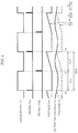
- FIG. 21 is a diagram showing an example of an integrated circuit of the switching regulator according to Embodiment 1.
- FIG. 1 is a configuration diagram of switching regulator 100 according to Embodiment 1, and input DC voltage Vi input to input terminal from DC voltage source 101 is stepped down and converted to output DC voltage Vo, and is supplied to load 102 from an output terminal. Additionally, a number is not assigned to the input terminal and the output terminal, and respective voltages Vi, Vo are assigned instead.
- Switching regulator 100 includes switch device 103 , diode 104 , inductor 105 , output capacitor 106 , and control circuit 107 .
- switch device 103 One end of switch device 103 is connected to input terminal Vi, and a cathode of diode 104 and one end of inductor 105 are connected to the other end.
- Inductor 105 is connected between switch device 103 and load 102 .
- An anode of diode 104 is grounded, and the other end of inductor 105 is connected to output terminal Vo.
- Output capacitor 106 is connected to output terminal Vo, in parallel with load 102 .
- Input DC voltage Vi is intermittently at high frequency due to switch device 103 , which is repeatedly turned on/off by drive signal Dr from control circuit 107 , and is smoothed by inductor 105 and output capacitor 106 , and output DC voltage Vo is thereby supplied to load 102 .
- switch device 103 When switch device 103 is in an off state, diode 104 forms a path allowing a reflux current of inductor 105 to flow to the output, and diode 104 is thus referred to also as a freewheeling diode.
- Switching regulator 100 having such a configuration is of a step-down type, and output DC voltage Vo is lower than input DC voltage Vi.
- TSW switching cycle of switch device 103
- Ton an on time as Ton
- a relationship between input DC voltage Vi and output DC voltage Vo of the step-down switching regulator is expressed by the following (Equation 1).
- Vo D ⁇ Vi (Equation 1)
- Control circuit 107 includes drive signal generation circuit 111 , hysteresis generation circuit 112 , and reference voltage generation circuit 113 .
- Drive signal generation circuit 111 includes comparator 131 , timer circuit 132 , and switch control circuit 133 , and receives application of input DC voltage Vi and output DC voltage Vo, and of reference voltage Vr from reference voltage generation circuit 113 , and generates drive signal Dr.
- Comparator 131 compares output DC voltage Vo with reference voltage Vr, and outputs output signal Vco indicating the comparison result.
- Timer circuit 132 measures a time length according to input DC voltage Vi and output DC voltage Vo, from inversion of output signal Vco, and outputs signal Vtim.
- Switch control circuit 133 generates drive signal Dr that turns on switch device 103 during a period from inversion of output signal Vco to rising of signal Vtim.
- Hysteresis generation circuit 112 includes current multiplier 141 , capacitor 142 , and switch 143 .
- Current multiplier 141 generates output current Iout according to input DC voltage Vi and output DC voltage Vo.
- Capacitor 142 is connected in parallel with an output terminal of current multiplier 141 , and is charged with output current Tout of current multiplier 141 .
- a charging voltage of capacitor 142 is given as voltage Vcr.
- Switch 143 is connected in parallel with capacitor 142 , and is turned on/off according to drive signal Dr. Switch 143 is turned on during a period when switch device 103 is turned on by drive signal Dr, and voltage Vcr of capacitor 142 is thereby reset to a GND level.
- Reference voltage generation circuit 113 includes reference voltage source 151 , resistor 152 , and voltage current converter 153 , and generates reference voltage Vr (pseudo ripple voltage) having a gradient proportional to output current Tout of current multiplier 141 .
- Reference voltage source 151 outputs stable DC voltage Vr 0 .
- Resistor 152 is connected between reference voltage source 151 and an input terminal of comparator 131 of drive signal generation circuit 111 .
- Voltage current converter 153 outputs a current that is proportional to voltage Vcr from hysteresis generation circuit 112 , and supplies the current to reference voltage source 151 through resistor 152 .
- FIG. 2 is a timing chart showing an operation of switching regulator 100 , and shows drive signal Dr, signal Vco, signal Vtim, reference voltage Vr, and output DC voltage Vo.
- timer circuit 132 measures on time Ton from time t 0 .
- T on TSW ⁇ Vo/Vi (Equation 2)
- timer circuit 132 measures on time Ton, which is proportional to output DC voltage Vo and inversely proportional to input DC voltage Vi, after output signal Vco is inverted.
- FIG. 3 is a diagram showing an example configuration of timer circuit 132 .
- Timer circuit 132 shown in FIG. 3 includes voltage current converter 161 , switch 162 , capacitor 163 , comparator 164 , and edge detection circuit 165 .
- Voltage current converter 161 outputs a current that is proportional to input DC voltage Vi.
- Capacitor 163 is connected to an output terminal of voltage current converter 161 , and generates voltage V 1 by being charged with the current from voltage current converter 161 .
- Switch 162 is connected in parallel with capacitor 163 , and on/off of switch 162 is controlled according to signal Vco.
- Comparator 164 compares output DC voltage Vo with voltage V 1 , and outputs signal V 2 indicating the comparison result.
- Edge detection circuit 165 detects a rising edge of signal V 2 , and generates signal Vtim indicating the detection result.
- FIG. 4 is a timing chart showing an operation of timer circuit 132 , and shows drive signal Dr, signal Vco, voltage V 1 and output DC voltage Vo, signal V 2 , and signal Vtim.
- signal Vco rises, and switch 162 is turned on and voltage V 1 is reset to the GND level.
- Signal Vco is a one-shot pulse, and thus, switch 162 is immediately turned off after resetting of voltage V 1 .
- capacitor 163 is charged with the current from voltage current converter 161 , and voltage V 1 rises.
- the current from voltage current converter 161 is proportional to input DC voltage Vi, and a rising speed of voltage V 1 is also proportional to input DC voltage Vi.
- output signal V 2 of comparator 164 rises, and edge detection circuit 165 raises one-shot pulse signal Vtim when detecting rising of signal V 2 .
- Rising of signal Vco to rising of signal Vtim corresponds to on time Ton. That is, up to charging of output DC voltage Vo at the rising speed proportional to input DC voltage Vi is on time Ton, and thus, on time Ton is inversely proportional to input DC voltage Vi and proportional to output DC voltage Vo (Ton ⁇ Vo/Vi).
- switch control circuit 133 When signal Vtim rises at time t 1 , which is after a lapse of on time Ton from time t 0 , switch control circuit 133 causes drive signal Dr to fall, and places switch device 103 in an off state.
- Switch 143 which is in an on state in the on period (t 0 to t 1 ) of drive signal Dr is placed in an off state at the time of fall of drive signal Dr at time t 1 .
- Capacitor 142 is thereby charged with output current Iout of current multiplier 141 , and voltage Vcr which is reset to the GND level starts to rise.
- Voltage current converter 153 outputs a current that is proportional to rising voltage Vcr, a voltage drop occurs at resistor 152 , and reference voltage Vr starts to rise from voltage Vr 0 .
- switch device 103 repeats a switching operation at switching cycle TSW, which is a sum of on time Ton and off time Toff.
- Amplitude ⁇ Vr of reference voltage Vr is constant ⁇ , as given by the following (Equation 5).
- both switching cycle TSW and amplitude ⁇ Vr of reference voltage Vr may be made constant regardless of input DC voltage Vi and output DC voltage Vo. If fluctuations in switching cycle TSW is suppressed, interference with radio frequency may be suppressed for vehicle-mounting usage in particular. If fluctuations in amplitude ⁇ Vr of reference voltage Vr is suppressed, a margin may be secured with respect to an input dynamic range of comparator 131 , for example. That is, switching regulator 100 may cover a wide range of input/output voltage.
- various electronic devices such as a semiconductor and a capacitor, configuring the system are increased in size to achieve a high breakdown voltage. Accordingly, to enable use of an electronic device with a 12V battery, a power supply device which steps down 48V to 12V becomes necessary.
- FIG. 5 is a diagram showing an example configuration of motor control system 200 according to the present embodiment.
- Motor control system 200 includes switching regulator 201 that steps down high voltage V 0 of about 48V to medium voltage V 1 of about 12V, switching regulator 202 that steps down voltage V 1 to voltage V 2 of about 6V, and switching regulator 203 that steps down voltage V 2 to low voltage V 3 of about 1.25V.
- Switching regulators 201 to 203 have a same configuration as switching regulator 100 in FIG. 1 .
- Battery 204 supplies voltage V 0 of about 48V to input terminal Vi of switching regulator 201 and power supply terminal Vi of motor 205 .
- Output voltage V 1 of switching regulator 201 is supplied to input terminal Vi of switching regulator 202 and pre-driver power supply terminal Vp of the motor.
- Output voltage V 2 of switching regulator 202 is supplied to input terminal Vi of switching regulator 203 and input terminal Vi of regulator 206 that supplies power for a low breakdown voltage device.
- Output voltage V 3 of switching regulator 203 is supplied to CPU power supply terminal VCC of motor control microcomputer 207 .
- switching regulator 201 has to perform stabilization control on output voltage V 1 with respect to such transient fluctuations in the input voltage.
- Regulator 206 is a power supply for a device which is sensitive to noise, such as a sensor, and thus, a low drop-out (LDO) regulator is used.
- LDO low drop-out
- a switching regulator with small fluctuations in output voltage, with respect to load fluctuations is desired as switching regulator 202 as a power supply for regulator 206 .
- a hysteresis control method which achieves high-speed responsiveness is particularly effective with respect to sudden load fluctuations.
- Microcomputer 207 has to be able to perform sophisticated arithmetic computations at a high speed in order to achieve a high-level safety function and lower fuel consumption, and thus, a high-performance CPU is installed. Processes at a fine rule level, with low parasitic capacitance, are used for such a CPU so as to accelerate an operation clock.
- a CPU is a CPU that operates at a power supply voltage of around 1V, and an allowable power supply voltage fluctuation range is extremely small at about 2.5%.
- current consumption in an operation mode of the CPU is high, and thus, a current sharply fluctuates at a time of switching from a standby mode to the operation mode. Accordingly, switching regulator 203 which is capable of swiftly responding to sharp load fluctuations, and which achieves small output voltage fluctuations is desired.
- switching regulator 100 As described above, by using switching regulator 100 according to the present embodiment, the following requirements may be satisfied: (1) to cope with a wide range of input voltage; and (2) to swiftly respond to load transient fluctuations (for example, about 2.5%). Moreover, fluctuations in the switching cycle may be suppressed, and occurrence of interference with radio frequency caused by fluctuations in a switching frequency (switching noise interference) may be suppressed.
- reference voltage Vr is changed only during an off period of drive signal Dr.
- a configuration for changing reference voltage Vr also in an on period, in addition to the off period of drive signal Dr, will be described. Additionally, in the following, differences from Embodiment 1 described above will be mainly described, and a redundant description will be omitted.
- FIG. 6 shows a configuration of switching regulator 100 A according to the present embodiment.
- a configuration of control circuit 107 A is different from that of control circuit 107 in FIG. 1 in that control circuit 107 A includes reset pulse generation circuit 124 .
- hysteresis generation circuit 112 A is different from that of hysteresis generation circuit 112 in that hysteresis generation circuit 112 A includes voltage source 144 and signal generation circuit 145 , and with respect to a function of current multiplier 141 A.
- Voltage source 144 is connected in series with switch 143 , and outputs voltage Er.
- Signal generation circuit 145 generates signal ON 1 , signal ON 2 and the like to be input to current multiplier 141 A.
- FIG. 7 is a timing chart showing an operation of switching regulator 100 A.
- Reset pulse generation circuit 124 generates reset pulse Vrst at a time of rising of drive signal Dr.
- Switch 143 is thereby temporarily turned on, and voltage Vcr of capacitor 142 is reset to voltage Er. Then, when switch 143 is turned off, voltage Vcr is reduced according to a current that is output from current multiplier 141 A.
- hysteresis generation circuit 112 A controls gradient ⁇ Von/ ⁇ T of voltage Vcr (i.e., gradient of reference voltage Vr) in an on period in a manner expressed by the following (Equation 6), with ⁇ as a proportionality constant. Additionally, the gradient indicated below is an absolute value of gradient.
- ⁇ V on/ ⁇ T ( ⁇ / TSW ) ⁇ ( Vi/Vo ) (Equation 6)
- output current Iout of current multiplier 141 A is a sink current that is proportional to Vi/Vo, and voltage Vcr (reference voltage Vr) is reduced at a gradient proportional to Vi/Vo.
- Amplitude ⁇ Vr of reference voltage Vr is constant and is equal to a proportionality constant ⁇ , as given by the above-described (Equation 2) and (Equation 6) and the following (Equation 7).
- amplitude ⁇ Vr takes a constant value regardless of input DC voltage Vi and output DC voltage Vo. Accordingly, as in Embodiment 1, the control circuit may cope with wide fluctuations in input DC voltage Vi and output DC voltage Vo.
- output current Tout of current multiplier 141 A is proportional to Vi/(Vi ⁇ Vo), and voltage Vcr (reference voltage Vr) rises at gradient ⁇ V/ ⁇ T proportional to Vi/(Vi ⁇ Vo) as expressed by (Equation 8), where ⁇ is given as a proportionality constant.
- ⁇ V/ ⁇ T ( ⁇ / TSW ) ⁇ Vi /( Vi ⁇ Vo ) (Equation 8)
- Amplitude ⁇ Vr of reference voltage Vr in the off period is constant, and is equal to proportionality constant ⁇ , as given by the above-described (Equation 3) and (Equation 8) and the following (Equation 9).
- switch device 103 repeats a switching operation at switching cycle TSW, which is a sum of on time Ton and off time Toff.
- Reference voltage Vr in (Equation 10) returns to voltage Vr 0 by a reset pulse at a rise of signal Vco. If reference voltage Vr becomes higher than voltage Vr 0 before reset, there is no offset voltage with respect to reference voltage Vr of comparator 131 before and after reset, and chattering occurs, thereby causing instability. Accordingly, constants ⁇ , ⁇ are set to be ⁇ > ⁇ .
- reference voltage Vr changes also in the on period, and thus, a pulse width of signal Vco which becomes high when reference voltage Vr is at or higher than output DC voltage Vo changes.
- the timing chart in FIG. 7 is a case where a high period of signal Vco is short, and output DC voltage Vo becomes higher than reference voltage Vr and signal Vco drops before on time Ton is measured by timer circuit 132 .
- the timing chart in FIG. 8 is a case where the high period of signal Vco is long, and signal Vco drops after on time Ton is measured.
- time t 0 to t 1 corresponding to Ton is referred to as a first on period, and the time is given as Ton 1 .
- Time t 1 to t 3 when signal Vco drops after a lapse of on time Ton 1 is referred to as a second on period, and the time is given as Ton 2 .
- Switch control circuit 133 generates drive signal Dr that turns on switch device 103 during a period from when reference voltage Vr reaches or exceeds output DC voltage Vo and output signal Vco rises, to a later one of (1) rising of signal Vtim after a lapse of on time Ton 1 , and (2) dropping of signal Vco after output DC voltage Vo becomes higher than reference voltage Vr.
- hysteresis generation circuit 112 A controls gradient ⁇ Von 2 / ⁇ T of voltage Vcr (i.e., gradient of reference voltage Vr) in the second on period in a manner expressed by the following (Equation 11), with ⁇ as a proportionality constant.
- ⁇ V on2/ ⁇ T ( ⁇ / TSW ) ⁇ ( Vi/Vo ) (Equation 11)
- constant ⁇ is set smaller than constant ⁇ . That is, output current Iout of current multiplier 141 A in the first on period is higher than output current Iout of current multiplier 141 A in the second on period, and the gradient of reference voltage Vr in the first on period is greater than the gradient of reference voltage Vr in the second on period. The amplitude of reference voltage Vr may thereby be prevented from becoming great even when the on period is long.
- a solid line indicates reference voltage Vr in a case where the gradient in the second on period is smaller than the gradient in the first on period
- a dotted line indicates reference voltage Vr in a case where the gradient in the second on period is the same as the gradient in the first on period.
- reference voltage Vr is more reduced as the on period becomes longer, and as a result, the amplitude of reference voltage Vr becomes great.
- the gradient in the second on period is made smaller than the gradient in the first on period, an increase in the amplitude may be suppressed.
- FIG. 10 is a circuit configuration diagram of current multiplier 141 A
- FIG. 11 is a timing chart of control signals that are input to current multiplier 141 A.
- Signal ON, signal ON 1 , signal ON 2 , and signal OFF shown in FIG. 11 are generated from signal Vco and signal Vtim by signal generation circuit 145 .
- Signal ON is a signal that reaches a high level in an on period (including the first on period and the second on period).
- Signal ON 1 is a signal that reaches a high level in the first on period.
- Signal ON 2 is a signal that reaches a high level in the second on period.
- Signal OFF is an inverted signal of signal ON, and is a signal that reaches a high level in the off period.
- current multiplier 141 A includes current source circuits 171 , 172 and 173 , multiplier 174 , and output current mirror circuit 175 .
- IVi is a current that is proportional to input DC voltage Vi
- Ivo is a current that is proportional to output DC voltage Vo.
- 2Ivo is a current that is twice Ivo
- Ia is a constant direct current.
- I(QN) Is ⁇ exp ⁇ VBE(QN)/(kT) ⁇ , and thus, relationships of the following (Equation 17) and (Equation 18) are established.
- I ( Q 1) ⁇ I ( Q 2) Is ⁇ exp ⁇ VBE ( Q 1)/ kT ⁇ Is ⁇ exp( VBE ( Q 2)/ kT ) (Equation 17)
- I ( Q 3) ⁇ I ( Q 4) Is ⁇ exp ⁇ VBE ( Q 3)/ kT ⁇ Is ⁇ exp( VBE ( Q 4)/ kT ) (Equation 18)
- I(Q 4 ), I(Q 3 ) are approximated in a manner expressed by the following (Equation 21) by using hFE>>1 of NPN.
- I ( Q 4) I 4
- I ( Q 3) ⁇ I 3 (Equation 21)
- output current Iout of current multiplier 141 A in the on period is proportional to Vi/Vo.
- output current Iout of current multiplier 141 A in the off period is proportional to (1 ⁇ Vo/Vi).
- a mirror ratio of output current mirror circuit 175 is set to ( ⁇ > ⁇ ). Accordingly, output current Iout in the second on period is lower than output current Iout in the first on period.
- FIG. 12 is a diagram which is the timing chart in FIG. 7 according to Embodiment 2, to which offset voltage Vof is added.
- An influence of offset voltage Vof on ratio Vo/Vi between input DC voltage Vi and output DC voltage Vo will be described with respect to a case where Vo/Vi is high, for example.
- FIG. 13 is a diagram which is the timing chart in FIG. 8 according to Embodiment 2, to which offset voltage Vof is added, and shows a case where signal Vco drops after a lapse of on time Ton.
- the amplitude of voltage Vr increases also during second on period Ton 2 after a lapse of on time Ton, and thus, offset voltage Vof is increased and output DC voltage Vo is reduced compared to a case where Vo/Vi is small.
- FIG. 14 is a diagram showing a configuration of switching regulator 100 B according to Embodiment 3. With switching regulator 100 B shown in FIG. 14 , a configuration of control circuit 107 B is different from that of control circuit 107 A shown in FIG. 6 , and correction circuit 114 that corrects output DC voltage Vo is provided.
- Correction circuit 114 is configured by amplifier 181 , which is a differential voltage input current amplifying/output device.
- Amplifier 181 compares output DC voltage Vo with voltage Vr 0 of reference voltage source 151 , and amplifies and generates an output current that is according to voltage difference (Vr 0 ⁇ Vo).
- An output of amplifier 181 is connected to resistor 152 and a positive input terminal of comparator 131 , and an output current of amplifier 181 flows through resistor 152 .
- FIG. 15 is a timing chart for switching regulator 100 B according to the present embodiment.
- output DC voltage Vo becomes higher than reference voltage Vr and Vco is dropped before a lapse of on time Ton measured by timer circuit 132 .
- FIG. 16 is a diagram showing a case where signal Vco drops after a lapse of on time Ton. Also in this case, correction circuit 114 compares output DC voltage Vo with voltage Vr 0 , which is an output voltage of reference voltage source 151 , and causes an output current to flow through resistor 152 . An operating point of reference voltage Vr is thereby corrected to cause the voltages to be approximately equal to each other, and offset voltage Vof is cancelled. As a result, fluctuations in the offset voltage caused by input/output voltage ratio Vo/Vi are eliminated.
- FIG. 17 is a configuration diagram of switching regulator 100 C according to a variation of the present embodiment.
- Switching regulator 100 C shown in FIG. 17 is different from switching regulator 100 B shown in FIG. 14 , with a configuration of correction circuit 114 C included in control circuit 107 C being different from the configuration of correction circuit 114 included in control circuit 107 B.
- Correction circuit 114 C includes amplifier 181 and resistor 182 .
- Resistor 182 is connected between output terminal Vo of switching regulator 100 C and a negative input terminal of comparator 131 of the drive signal generation circuit.
- output DC voltage Vo is applied to a positive input terminal
- a negative input terminal is connected to reference voltage source 151
- an output terminal is connected to a connection point of resistor 182 and the negative input terminal of comparator 131 .
- FIG. 18 is a timing chart for switching regulator 100 C shown in FIG. 17 . If output voltage correction is not performed, reference voltage Vr and output DC voltage Vo become equal to each other at time t 2 , and an output signal of comparator 131 is inverted. At this time, because reference voltage (in the drawing, voltage of resistor 152 ) Vr is reset to voltage Vr 0 of reference voltage source 151 . Because voltage Vr is set to be inevitably lower than voltage Vr 0 , offset voltage Vof is caused for output DC voltage Vo with respect to voltage Vr 0 .
- a voltage at the positive input terminal of amplifier 181 of correction circuit 114 C is reduced by offset voltage Vof, and amplifier 181 of correction circuit 114 C outputs a current in a negative direction.
- Voltage Va at the negative input terminal of comparator 131 is reduced, by the negative current, from output DC voltage Vo by the amount of voltage drop at resistor 182 .
- Output DC voltage Vo is thus controlled in a direction of rising.
- an operating point of voltage Vr is corrected by correction circuit 114 or 114 C to thereby reduce fluctuations in the output voltage caused by fluctuations in the input voltage.
- FIG. 19 is a configuration diagram of switching regulator 100 D according to Embodiment 4.
- switching regulator 100 D shown in FIG. 19 a configuration of reference voltage generation circuit 113 D included in control circuit 107 D is different from that of reference voltage generation circuit 113 included in control circuit 107 A shown in FIG. 6 , and also, voltage current converter 153 D of a differential current output type and resistor 182 are provided.
- Resistor 182 shown in FIG. 19 is connected between an output terminal where output DC voltage Vo is output, and a negative input terminal of comparator 131 .
- Output voltage Vcr of current multiplier 141 A is applied to an input terminal of voltage current converter 153 D.
- Voltage current converter 153 D outputs a current that is proportional to ⁇ . Vcr to a positive output terminal, and outputs a current that is proportional to ⁇ . Vcr to a negative output terminal.
- Positive output current Ivr+ of voltage current converter 153 D is supplied to a connection point of a positive input terminal of comparator 131 and resistor 152
- negative output current Ivr ⁇ is supplied to a connection point of the negative input terminal of comparator 131 and resistor 182 .
- FIG. 20 is a timing chart for switching regulator 100 D according to the present embodiment.
- positive input voltage Vr of comparator 131 is reset to voltage Vr 0
- negative input voltage Va is reset to output DC voltage Vo.
- an input differential voltage amplitude of comparator 131 may be reduced to half by reducing an output current of voltage current converter 153 to half, but in this case, differential voltage ⁇ Vh 1 between reference voltage Vr of comparator 131 at the time of detection and reference voltage Vr after reset is also reduced to half.
- Embodiment 4 a differential voltage between the time of detection and after reset of positive input voltage Vr is reduced to half, and a differential voltage between the time of detection and after reset of negative input voltage Va is reduced to half, but comparator 131 detects a positive/negative input voltage difference, and thus voltage difference ⁇ Vh 2 between the time of detection and after reset is the same as in Embodiment 2.
- a voltage amplitude of reference voltage Vr is reduced such that stable operation may be performed even if an input dynamic range of comparator 131 is reduced. Accordingly, the configuration of the present embodiment is advantageous especially in the case of low-voltage operation.
- switching regulators 100 , 100 A, 100 B, 100 C, and 100 D are wholly or partly implemented as an LSI, which is an integrated circuit. These may be separate individual chips, or may be partly or wholly contained on one chip.
- switch device 103 , diode 104 , and control circuit 107 may be contained on one chip.
- One chip is advantageous in that the system may be miniaturized due to reduction in the number of components.
- switch device 103 and diode 104 are heat sources. Accordingly, it is important to optimize the configuration according to use.
- FIG. 21 shows an example of switching regulator 100 according to Embodiment 1, but the same thing applies also to switching regulator 100 A according to Embodiment 2, switching regulators 100 B, 100 C according to Embodiment 3, and switching regulator 100 D according to Embodiment 4.
- the means for circuit integration is not limited to an LSI, and implementation by a dedicated circuit or a general-purpose processor is also possible.
- a field programmable gate array (FPGA), which is programmable after the LSI is manufactured, or a reconfigurable processor in which connections and settings of circuit cells within the LSI are reconfigurable may also be used.
- the circuit configurations shown in the circuit diagrams described above are merely examples, and the present disclosure is not limited to the circuit configurations described above. That is, a circuit which is capable of realizing characteristic functions of the present disclosure, in the same manner as with the circuit configurations described above, is also included in the present disclosure.
- the present disclosure includes an element to which an element such as a switching element (transistor), a resistive element, or a capacitance element is connected in series or in parallel, so long as the same functions as those of the circuit configurations described above can be realized.
- connection in the embodiments described above is not limited to a case where two terminals (nodes) are directly connected, but also includes a case where the two terminals (nodes) are connected via an element, so long as the same functions can be realized.
- a logic level represented by high/low or a switching state represented by on/off is presented as an example to specifically describe the present disclosure, and an equivalent effect may be obtained by different combinations of exemplified logic levels or switching states.
- the configurations of the above-described logic circuit are presented as examples to specifically describe the present disclosure, and an equivalent input/output relationship may be realized by a logic circuit having a different configuration.
- An n-type, a p-type, and the like of the transistor and the like are used as examples to specifically describe the present disclosure, and the present disclosure is not limited thereto.
- circuit blocks in the block diagrams and the like are merely examples, and a plurality of functional blocks may be implemented in one functional block, or one functional block may be divided into a plurality of blocks, or a part of the functions may be moved to a different functional block.
- MOS transistor or bipolar transistor the type of transistor described above (MOS transistor or bipolar transistor) is merely an example, and a different type of transistor may also be used.
- the present disclosure may be applied to a switching regulator, and is especially useful for a switching regulator of a vehicle-mounted microcomputer power supply.
Landscapes
- Engineering & Computer Science (AREA)
- Power Engineering (AREA)
- Dc-Dc Converters (AREA)
Abstract
Description
Vo=D·Vi (Equation 1)
Ton=TSW·Vo/Vi (Equation 2)
Toff=TSW−Ton=TSW·(1−Vo/Vi) (Equation 3)
ΔV/ΔT=(α/TSW)·(Vi/(Vi−Vo)) (Equation 4)
ΔVon/ΔT=(α/TSW)·(Vi/Vo) (Equation 6)
ΔV/ΔT=(γ/TSW)−Vi/(Vi−Vo) (Equation 8)
Vr=Vr0−α+γ (Equation 10)
ΔVon2/ΔT=(β/TSW)·(Vi/Vo) (Equation 11)
I1=Ivo+Ia, I2=IVi−Ia, I3=−Ivo (Equation 12)
I1=IVi+Ia−IVo, I2=IVi−Ia, I3=IVo−IVi (Equation 13)
I(Q3)+I(Q1)=I1, I(Q2)=I(Q1)+I2 (Equation 14)
∴I(Q2)=−I(Q3)+I1+I2 (Equation 15)
VBE(Q1)+VBE(Q2)=VBE(Q3)+VBE(Q4) (Equation 16)
I(Q1)×I(Q2)=Is·exp{VBE(Q1)/kT}×Is·exp(VBE(Q2)/kT) (Equation 17)
I(Q3)×I(Q4)=Is·exp{VBE(Q3)/kT}×Is·exp(VBE(Q4)/kT) (Equation 18)
I(Q4)=I(Q1)×I(Q2)/I(Q3) (Equation 19)
I(Q4)=(−I(Q3)+I1)·(−I(Q3)+I1+I2)/I(Q3) (Equation 20)
I(Q4)=I4, I(Q3)=−I3 (Equation 21)
I4=−(I3+I1)·(I3+I1+I2)/I3 (Equation 22)
I4=−(−Ivo+Ivo+Ia)·(−Ivo+Ivo+Ia+Ivi−Ia)/(−Ivo)=Ia·(Ivi/Ivo) (Equation 23)
Iout∝Vi/Vo∝(1/Ton) (Equation 24)
I4=−(Ia)·(Ivi)/(Ivo−Ivi)=Ia/(1−Ivo/Ivi) (Equation 25)
Iout∝1(1−Vo/Vi)∝(1/Toff) (Equation 26)
ΔVr2=Va−Vr=−(Vr0−Vo)+Vcr·Ton (Equation 27)
Claims (13)
Applications Claiming Priority (4)
| Application Number | Priority Date | Filing Date | Title |
|---|---|---|---|
| JP2016-150342 | 2016-07-29 | ||
| JP2016150342 | 2016-07-29 | ||
| JPJP2016-150342 | 2016-07-29 | ||
| PCT/JP2017/026421 WO2018021172A1 (en) | 2016-07-29 | 2017-07-21 | Switching regulator |
Related Parent Applications (1)
| Application Number | Title | Priority Date | Filing Date |
|---|---|---|---|
| PCT/JP2017/026421 Continuation WO2018021172A1 (en) | 2016-07-29 | 2017-07-21 | Switching regulator |
Publications (2)
| Publication Number | Publication Date |
|---|---|
| US20190157973A1 US20190157973A1 (en) | 2019-05-23 |
| US10951115B2 true US10951115B2 (en) | 2021-03-16 |
Family
ID=61017065
Family Applications (1)
| Application Number | Title | Priority Date | Filing Date |
|---|---|---|---|
| US16/255,319 Active 2038-03-30 US10951115B2 (en) | 2016-07-29 | 2019-01-23 | Switching regulator |
Country Status (4)
| Country | Link |
|---|---|
| US (1) | US10951115B2 (en) |
| JP (1) | JP6964585B2 (en) |
| CN (1) | CN109478847B (en) |
| WO (1) | WO2018021172A1 (en) |
Families Citing this family (4)
| Publication number | Priority date | Publication date | Assignee | Title |
|---|---|---|---|---|
| TWI750357B (en) * | 2018-03-23 | 2021-12-21 | 力智電子股份有限公司 | Current mirror calibration circuit and current mirror calibration method |
| CN115191080A (en) * | 2020-04-01 | 2022-10-14 | 德州仪器公司 | Constant ripple injection circuit for switching converter |
| JP7568586B2 (en) * | 2021-06-16 | 2024-10-16 | 株式会社Tmeic | DC/DC conversion device |
| TWI842128B (en) * | 2022-10-14 | 2024-05-11 | 立錡科技股份有限公司 | Switching regulator and operation clock signal generator circuit and control method thereof |
Citations (4)
| Publication number | Priority date | Publication date | Assignee | Title |
|---|---|---|---|---|
| US20070063685A1 (en) | 2005-09-21 | 2007-03-22 | Takuya Ishii | DC-DC converter |
| US7279875B2 (en) * | 2005-06-16 | 2007-10-09 | Ge Gan | High switching frequency DC-DC converter with fast response time |
| US20120025919A1 (en) | 2010-07-28 | 2012-02-02 | Active-Semi, Inc. | Synchronization of multiple high frequency switching power converters in an integrated circuit |
| US8138739B1 (en) | 2008-10-03 | 2012-03-20 | Fairchild Semiconductor Corporation | Circuits and methods for improving transient response of hysteretic DC-DC converters |
Family Cites Families (4)
| Publication number | Priority date | Publication date | Assignee | Title |
|---|---|---|---|---|
| CN102097934A (en) * | 2011-02-25 | 2011-06-15 | 浙江大学 | Hysteresis mode buck DC/DC (direct current/direct current) switch converter |
| US8704587B2 (en) * | 2012-07-23 | 2014-04-22 | Freescale Semiconductor, Inc. | Configurable multistage charge pump using a supply detect scheme |
| CN103036432B (en) * | 2012-12-07 | 2015-02-25 | 上海电力学院 | Pulse width modulation (PWM) hysteresis control method based on ripple |
| US20160204702A1 (en) * | 2015-01-08 | 2016-07-14 | Broadcom Corporation | Low Output Ripple Adaptive Switching Voltage Regulator |
-
2017
- 2017-07-21 JP JP2018529840A patent/JP6964585B2/en active Active
- 2017-07-21 CN CN201780045514.0A patent/CN109478847B/en active Active
- 2017-07-21 WO PCT/JP2017/026421 patent/WO2018021172A1/en not_active Ceased
-
2019
- 2019-01-23 US US16/255,319 patent/US10951115B2/en active Active
Patent Citations (6)
| Publication number | Priority date | Publication date | Assignee | Title |
|---|---|---|---|---|
| US7279875B2 (en) * | 2005-06-16 | 2007-10-09 | Ge Gan | High switching frequency DC-DC converter with fast response time |
| US20070063685A1 (en) | 2005-09-21 | 2007-03-22 | Takuya Ishii | DC-DC converter |
| JP2007089278A (en) | 2005-09-21 | 2007-04-05 | Matsushita Electric Ind Co Ltd | DC-DC converter |
| US8138739B1 (en) | 2008-10-03 | 2012-03-20 | Fairchild Semiconductor Corporation | Circuits and methods for improving transient response of hysteretic DC-DC converters |
| US20120025919A1 (en) | 2010-07-28 | 2012-02-02 | Active-Semi, Inc. | Synchronization of multiple high frequency switching power converters in an integrated circuit |
| US8164391B2 (en) * | 2010-07-28 | 2012-04-24 | Active-Semi, Inc. | Synchronization of multiple high frequency switching power converters in an integrated circuit |
Non-Patent Citations (1)
| Title |
|---|
| International Search Report and Written Opinion issued in International Patent Application No. PCT/JP2017/026421, dated Aug. 15, 2017; with partial English translation. |
Also Published As
| Publication number | Publication date |
|---|---|
| CN109478847A (en) | 2019-03-15 |
| WO2018021172A1 (en) | 2018-02-01 |
| US20190157973A1 (en) | 2019-05-23 |
| CN109478847B (en) | 2021-02-26 |
| JP6964585B2 (en) | 2021-11-10 |
| JPWO2018021172A1 (en) | 2019-05-09 |
Similar Documents
| Publication | Publication Date | Title |
|---|---|---|
| US10951115B2 (en) | Switching regulator | |
| JP2021518061A (en) | Low quiescent current load switch | |
| US8933682B2 (en) | Bandgap voltage reference circuit | |
| JP2006053898A (en) | Overcurrent protection circuit and voltage generation circuit and electronic equipment using it | |
| JP2012088987A (en) | Semiconductor integrated circuit for regulators | |
| WO2006016456A1 (en) | Circuit protection method, protection circuit and power supply device using the protection circuit | |
| JP2013012000A (en) | Semiconductor integrated circuit for regulator | |
| US9606556B2 (en) | Semiconductor integrated circuit for regulator | |
| US10591941B2 (en) | Low dropout regulator with wide input supply voltage | |
| KR102225712B1 (en) | Voltage regulator | |
| US20080265856A1 (en) | Constant-voltage power circuit | |
| US20220011800A1 (en) | Asynchronous Non-Linear Control of Digital Linear Voltage Regulator | |
| JP2017134743A (en) | Regulator circuit | |
| US20210165437A1 (en) | Asynchronous Non-Linear Control of Digital Linear Voltage Regulator | |
| TWI672572B (en) | Voltage Regulator | |
| Rincon-Mora et al. | Study and design of low drop-out regulators | |
| US7495504B2 (en) | Reference voltage generation circuit | |
| JP2020166648A (en) | Reference voltage generation circuit and semiconductor device | |
| JP2018102023A (en) | Overcurrent detection circuit, semiconductor device, and power supply device | |
| US11342737B2 (en) | Short-circuit-protected low-dropout linear regulator | |
| JP3833440B2 (en) | Voltage generation circuit, voltage regulator, and portable terminal device using them | |
| US20240272665A1 (en) | Low-dropout regulator and operation method | |
| US20250103077A1 (en) | Control Circuitry For Parallel-Operating Voltage Regulators | |
| JP2009093446A (en) | Voltage control circuit | |
| JP2013196497A (en) | Voltage regulator |
Legal Events
| Date | Code | Title | Description |
|---|---|---|---|
| FEPP | Fee payment procedure |
Free format text: ENTITY STATUS SET TO UNDISCOUNTED (ORIGINAL EVENT CODE: BIG.); ENTITY STATUS OF PATENT OWNER: LARGE ENTITY |
|
| STPP | Information on status: patent application and granting procedure in general |
Free format text: DOCKETED NEW CASE - READY FOR EXAMINATION |
|
| AS | Assignment |
Owner name: PANASONIC INTELLECTUAL PROPERTY MANAGEMENT CO., LT Free format text: ASSIGNMENT OF ASSIGNORS INTEREST;ASSIGNORS:MIHASHI, TETSUYA;ISHIYAMA, JUNJI;REEL/FRAME:049673/0791 Effective date: 20181225 Owner name: PANASONIC INTELLECTUAL PROPERTY MANAGEMENT CO., LTD., JAPAN Free format text: ASSIGNMENT OF ASSIGNORS INTEREST;ASSIGNORS:MIHASHI, TETSUYA;ISHIYAMA, JUNJI;REEL/FRAME:049673/0791 Effective date: 20181225 |
|
| AS | Assignment |
Owner name: PANASONIC SEMICONDUCTOR SOLUTIONS CO., LTD., JAPAN Free format text: ASSIGNMENT OF ASSIGNORS INTEREST;ASSIGNOR:PANASONIC INTELLECTUAL PROPERTY MANAGEMENT CO., LTD.;REEL/FRAME:052755/0870 Effective date: 20200521 |
|
| STCF | Information on status: patent grant |
Free format text: PATENTED CASE |
|
| AS | Assignment |
Owner name: NUVOTON TECHNOLOGY CORPORATION JAPAN, JAPAN Free format text: CHANGE OF NAME;ASSIGNOR:PANASONIC SEMICONDUCTOR SOLUTIONS CO., LTD.;REEL/FRAME:056245/0395 Effective date: 20201125 |
|
| MAFP | Maintenance fee payment |
Free format text: PAYMENT OF MAINTENANCE FEE, 4TH YEAR, LARGE ENTITY (ORIGINAL EVENT CODE: M1551); ENTITY STATUS OF PATENT OWNER: LARGE ENTITY Year of fee payment: 4 |