US10936119B2 - Self capacitance sensing based on tangent of phase shift of drive signal - Google Patents
Self capacitance sensing based on tangent of phase shift of drive signal Download PDFInfo
- Publication number
- US10936119B2 US10936119B2 US16/788,417 US202016788417A US10936119B2 US 10936119 B2 US10936119 B2 US 10936119B2 US 202016788417 A US202016788417 A US 202016788417A US 10936119 B2 US10936119 B2 US 10936119B2
- Authority
- US
- United States
- Prior art keywords
- samples
- voltage
- tangent
- phase shift
- conductive line
- Prior art date
- Legal status (The legal status is an assumption and is not a legal conclusion. Google has not performed a legal analysis and makes no representation as to the accuracy of the status listed.)
- Active
Links
Images


Classifications
-
- G—PHYSICS
- G06—COMPUTING OR CALCULATING; COUNTING
- G06F—ELECTRIC DIGITAL DATA PROCESSING
- G06F3/00—Input arrangements for transferring data to be processed into a form capable of being handled by the computer; Output arrangements for transferring data from processing unit to output unit, e.g. interface arrangements
- G06F3/01—Input arrangements or combined input and output arrangements for interaction between user and computer
- G06F3/03—Arrangements for converting the position or the displacement of a member into a coded form
- G06F3/041—Digitisers, e.g. for touch screens or touch pads, characterised by the transducing means
- G06F3/0416—Control or interface arrangements specially adapted for digitisers
- G06F3/04166—Details of scanning methods, e.g. sampling time, grouping of sub areas or time sharing with display driving
- G06F3/041662—Details of scanning methods, e.g. sampling time, grouping of sub areas or time sharing with display driving using alternate mutual and self-capacitive scanning
-
- G—PHYSICS
- G06—COMPUTING OR CALCULATING; COUNTING
- G06F—ELECTRIC DIGITAL DATA PROCESSING
- G06F3/00—Input arrangements for transferring data to be processed into a form capable of being handled by the computer; Output arrangements for transferring data from processing unit to output unit, e.g. interface arrangements
- G06F3/01—Input arrangements or combined input and output arrangements for interaction between user and computer
- G06F3/03—Arrangements for converting the position or the displacement of a member into a coded form
- G06F3/041—Digitisers, e.g. for touch screens or touch pads, characterised by the transducing means
- G06F3/044—Digitisers, e.g. for touch screens or touch pads, characterised by the transducing means by capacitive means
- G06F3/0446—Digitisers, e.g. for touch screens or touch pads, characterised by the transducing means by capacitive means using a grid-like structure of electrodes in at least two directions, e.g. using row and column electrodes
-
- G—PHYSICS
- G06—COMPUTING OR CALCULATING; COUNTING
- G06F—ELECTRIC DIGITAL DATA PROCESSING
- G06F3/00—Input arrangements for transferring data to be processed into a form capable of being handled by the computer; Output arrangements for transferring data from processing unit to output unit, e.g. interface arrangements
- G06F3/01—Input arrangements or combined input and output arrangements for interaction between user and computer
- G06F3/03—Arrangements for converting the position or the displacement of a member into a coded form
- G06F3/041—Digitisers, e.g. for touch screens or touch pads, characterised by the transducing means
- G06F3/0416—Control or interface arrangements specially adapted for digitisers
- G06F3/04166—Details of scanning methods, e.g. sampling time, grouping of sub areas or time sharing with display driving
-
- G—PHYSICS
- G06—COMPUTING OR CALCULATING; COUNTING
- G06F—ELECTRIC DIGITAL DATA PROCESSING
- G06F3/00—Input arrangements for transferring data to be processed into a form capable of being handled by the computer; Output arrangements for transferring data from processing unit to output unit, e.g. interface arrangements
- G06F3/01—Input arrangements or combined input and output arrangements for interaction between user and computer
- G06F3/03—Arrangements for converting the position or the displacement of a member into a coded form
- G06F3/041—Digitisers, e.g. for touch screens or touch pads, characterised by the transducing means
- G06F3/044—Digitisers, e.g. for touch screens or touch pads, characterised by the transducing means by capacitive means
Definitions
- This disclosure is directed to the field of self capacitance sensing and, in particular, to hardware and techniques for operating that hardware without the use of switched capacitor circuits.
- Touch screen devices are prevalent in today's computing environment. Portable computers, desktop computers, tablets, smart phones, and smartwatches typically employ a touch screen to gain user input for navigation and control of these devices. Thus, discerning the intent of the user via touch inputs is an important feature of a touch screen device.
- Touch screens typically operate based on capacitive touch sensing, and include a patterned array of conductive features.
- the patterned array of conductive features may include sets of lines, conductive pads, overlapping structures, interleaved structures, diamond structures, lattice structures, and the like.
- Two common capacitive touch sensing techniques or modes that may be performed on touch screens are mutual capacitance sensing and self capacitance sensing.
- a drive signal is applied to a subset of the lines referred to as drive lines, and capacitance values are measured at a subset of the lines referred to as sense lines, with it being understood that the sense lines cross the drive lines in a spaced apart fashion therefrom. Each crossing of drive line and sense line forms a capacitive node.
- the output of mutual capacitance sensing is a two-dimensional matrix of values, with one value for each capacitive node (crossing between drive line and sense line).
- the signal to noise ratio when measuring a single capacitive node is low. Therefore, the sensitivity of mutual touch sensing is not ideal for some situations.
- the drive signal is applied to every line, regardless of orientation. Bringing a finger or conductive stylus near the surface of the touch screen changes the local electric field, increasing the capacitance between the drive line or sense line of interest and ground (the “self capacitance”) in this instance.
- the self capacitance since all lines are driven, the capacitance change can only be measured on a per line basis as opposed to a per capacitive node basis. Therefore, the output of self capacitance sensing is two one dimensional arrays of values, with one value for each line.
- the signal to noise ratio when measuring an entire line is higher than when measuring a single capacitive node, and therefore self capacitance sensing allows for more precise measurements, albeit with an inability to resolve touches by more than a single finger accurately.
- a first aspect is directed to a touch screen controller including driving circuitry coupled to a conductive line through a resistance and configured to drive that conductive line with a driving signal forced through the resistance at a drive frequency, and sensing circuitry coupled to that conductive line and configured to sense a voltage at that conductive line, the voltage being a function of a capacitance seen by that conductive line.
- Analog to digital conversion circuitry is coupled to the sensing circuitry and configured to sample the sensed voltage at a sampling frequency to produce samples.
- Processing circuitry is coupled to the analog to digital conversion circuitry and configured to directly calculate a tangent of a phase shift of the voltage due to the resistance and the capacitance from the samples and determine a self touch value for that conductive line as a function of the tangent of the phase shift of the voltage.
- the sampling frequency may be greater than the drive frequency.
- the sampling frequency may be fixed.
- the processing circuitry may be configured to directly calculate the tangent of the phase shift of the voltage by performing a Fast Fourier Transform (FFT) as a function of the drive frequency to determine real and imaginary components of a signal represented by the samples, and determining the tangent of the phase shift of the voltage as a ratio of the real component of the signal represented by the samples to the imaginary component of the signal represented by the samples.
- FFT Fast Fourier Transform
- the processing circuitry may be configured to directly calculate the tangent of the phase shift of the voltage by multiplying the samples by a real multiplier and by an imaginary multiplier, summing the samples after multiplication to produce the signal represented by the samples, determining real and imaginary components of the signal represented by the samples, and determining the tangent of the phase shift of the voltage as the ratio of the real and imaginary components of the signal represented by the samples.
- the processing circuitry may perform the FFT by calculating the signal S represented by the samples at the drive frequency K as:
- the processing circuitry may perform the FFT by calculating the signal S represented by the samples at the drive frequency K as:
- the method includes driving a plurality of conductive lines with a drive signal forced through a resistance at a drive frequency. For each of the plurality of conductive lines, during a single self sensing frame, the method includes sampling a voltage at that conductive line at a sampling frequency to produce samples, the voltage being a function of a capacitance seen by that conductive line, directly calculating a tangent of a phase shift of the voltage due to the resistance and capacitance from the samples, and determining a self touch value for that conductive line during the self sensing frame as a function of the tangent of the phase shift of the voltage.
- the sampling frequency may be greater than the drive frequency.
- the sampling frequency may be fixed.
- the tangent of the phase shift of the voltage may be directly calculated by performing a Fast Fourier Transform (FFT) as a function of the drive frequency to determine real and imaginary components of a signal represented by the samples, and calculating the tangent of the phase shift of the voltage as a ratio of the real component of the signal represented by the samples to the imaginary component of the signal represented by the samples.
- FFT Fast Fourier Transform
- the tangent of the phase shift of the voltage may be determined by multiplying the samples by a real multiplier and by an imaginary multiplier, summing the samples after multiplication to produce the signal represented by the samples, determining real and imaginary components of the signal represented by the samples, and calculating the tangent of the phase shift of the voltage as the ratio of the real and imaginary components of the signal represented by the samples.
- Performing the FFT may include calculating the signal S represented by the samples at the drive frequency K as:
- Performing the FFT may include calculating the signal S represented by the samples at the drive frequency K as:
- a touch screen controller including driving circuitry coupled to a conductive line and configured to drive that conductive line, and sensing circuitry coupled to that conductive line and configured to sense a voltage at that conductive line, the voltage being a function of a capacitance seen by that conductive line.
- the touch screen controller also includes analog to digital conversion circuitry coupled to the sensing circuitry and configured to sample the sensed voltage to produce samples, and processing circuitry configured to determine a self touch value for that conductive line as a function of a tangent of a phase shift of the voltage.
- the processing circuitry may be configured to directly calculate the tangent of the phase shift of the voltage by performing a Fast Fourier Transform (FFT) to determine real and imaginary components of a signal represented by the samples, and determining the tangent of the phase shift of the voltage as a ratio of the real component of the signal represented by the samples to the imaginary component of the signal represented by the samples.
- FFT Fast Fourier Transform
- the processing circuitry may be configured to directly calculate the tangent of the phase shift of the voltage by multiplying the samples by a real multiplier and by an imaginary multiplier, summing the samples after multiplication to produce the signal represented by the samples, determining real and imaginary components of the signal represented by the samples, and determining the tangent of the phase shift of the voltage as the ratio of the real and imaginary components of the signal represented by the samples.
- the method includes driving conductive lines with a drive signal.
- the method also includes, for each of the conductive lines, during a single touch sensing frame, sampling a voltage at that conductive line to produce samples, the voltage being a function of a capacitance seen by that conductive line, directly calculating a tangent of a phase shift of the voltage due to the capacitance from the samples, and determining a touch value for that conductive line during the single touch sensing frame as a function of the tangent of the phase shift of the voltage.
- the tangent of the phase shift of the voltage may be directly calculated by performing a Fast Fourier Transform (FFT) to determine real and imaginary components of a signal represented by the samples, and calculating the tangent of the phase shift of the voltage as a ratio of the real component of the signal represented by the samples to the imaginary component of the signal represented by the samples.
- FFT Fast Fourier Transform
- the tangent of the phase shift of the voltage may be determined by multiplying the samples by a real multiplier and by an imaginary multiplier, summing the samples after multiplication to produce the signal represented by the samples, and calculating the tangent of the phase shift of the voltage as the ratio of the real and imaginary components of the signal represented by the samples.
- FIG. 1 is a block diagram of a touch screen device disclosed herein.
- FIG. 2 is a cross sectional view of the touch screen of the touch screen device of FIG. 1 .
- FIG. 3 is a diagram of the conductive columns and lines of the touch screen of FIGS. 1-2 .
- FIG. 4 is a flowchart of a method of operating the touch screen device of FIG. 1 for self capacitance sensing.
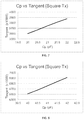
- FIG. 5 is a first graph of capacitance value of the capacitance of the RC circuit of FIG. 1 versus the tangent of a phase shift of the voltage across the RC circuit for a sine wave drive signal, in an ideal case.
- FIG. 6 is a second graph of capacitance value of the capacitance of the RC circuit of FIG. 1 versus the tangent of a phase shift of the voltage across the RC circuit for a sine wave drive signal, in an ideal case.
- FIG. 7 is a first graph of capacitance value of the capacitance of the RC circuit of FIG. 1 versus the tangent of a phase shift of the voltage across the RC circuit for a square wave drive signal, in an ideal case.
- FIG. 8 is a second graph of capacitance value of the capacitance of the RC circuit of FIG. 1 versus the tangent of a phase shift of the voltage across the RC circuit for a square wave drive signal, in an ideal case.
- FIG. 9 is a first graph of capacitance value of the capacitance of the RC circuit of FIG. 1 versus the tangent of a phase shift of the voltage across the RC circuit for a sine wave drive signal, in a real case.
- FIG. 10 is a second graph of capacitance value of the capacitance of the RC circuit of FIG. 1 versus the tangent of a phase shift of the voltage across the RC circuit for a sine wave drive signal, in a real case.
- FIG. 11 is a first graph of capacitance value of the capacitance of the RC circuit of FIG. 1 versus the tangent of a phase shift of the voltage across the RC circuit for a square wave drive signal, in a real case.
- FIG. 12 is a second graph of capacitance value of the capacitance of the RC circuit of FIG. 1 versus the tangent of a phase shift of the voltage across the RC circuit for a square wave drive signal, in a real case.
- FIG. 1 is a functional block diagram of a touch screen device 100 according to an embodiment as disclosed herein.
- the touch screen device 100 may be a smartphone, tablet, portable computer, smartwatch, wearable, or other device.
- the touch screen device 100 includes a tactile input surface, such as a touch screen display 110 , coupled to a touch screen controller 120 , which in turn is coupled to a system on a chip (SOC) 130 .
- SOC system on a chip
- the touch screen display 110 is designed to receive touch inputs from a user through a user's fingers or a stylus.
- the touch screen display 110 includes a display layer 113 and a touch sensing layer 111 (shown in FIG. 2 ) on the display layer 113 or spaced apart therefrom by another layer (not shown).
- the touch sensing layer 111 is comprised of parallel conductive rows (Rx) crossed by parallel conductive columns (Cy) (shown in FIG. 3 ). This crossing is in a spaced apart fashion such that the conductive rows do not make physical contact with the conductive columns.
- FIG. 1 for simplicity, but one conductive line, row R 1 , is shown. Also note that but one instance of drive circuitry 121 , resistance R, amplifier 125 , and ADC 122 are shown are shown for simplicity. However, note that, in actuality, the touch screen 110 in FIG. 1 contains any number of conductive rows and columns, as shown in the touch sensing layer 111 of FIG. 3 . Also note that, in actuality, for each instance of a conductive row and conductive column, there may be a drive circuitry, resistance, amplifier, and ADC.
- each conductive row and each conductive column has its own drive circuitry, resistance, amplifier, and ADC, or two or more rows (or two or more columns) may share a drive circuitry, resistance, amplifier, and ADC using a switching matrix (not shown).
- Drive circuitry 121 under control of processing circuitry 124 , generates a periodic drive signal (square wave or sine wave) and passes it to the conductive row R 1 through a resistance R.
- a capacitance C is formed between the conductive row R 1 and ground, and that this capacitance C changes based on proximity of a user's finger or a stylus to the conductive row R 1 .
- resistance R and capacitance C therefore form an RC circuit
- amplifier 125 is coupled to conductive row R 1 to receive input from the center tap of the RC circuit formed by resistance R and capacitance C.
- Amplifier 125 is directly electrically coupled to row R 1 , and amplifies and preprocesses the signal at row R 1 .
- Analog to digital converter (ADC) 122 receives the signal from the amplifier 125 and digitizes that signal. Note that the sampling frequency of the ADC 122 is greater than the frequency of the drive signal.
- Processing circuitry 124 receives the digitized signal from the ADC 122 , and from that digitized signal calculates a self capacitance strength value (referred to hereinafter simply as a strength value) for row R 1 during each sampling cycle. Calculated strength values are directly passed to SOC 130 by the processing circuitry 124 , or the processing circuitry 124 determines coordinates of a touch to the touch screen 110 from all the strength values calculated during each sampling cycle (keeping in mind that while only a single row R 1 was shown in FIG. 1 , in actuality there are many rows and columns in the touch screen 110 , and a single strength value for each row and for each column are determined during each sampling cycle) and passes the coordinates to the SOC 130 . From the received data (whether it be strength values or a coordinate or coordinates), the SOC 130 then takes action.
- a self capacitance strength value referred to hereinafter simply as a strength value
- Step 201 is comprised of sub-steps 202 , 204 , 206 , and 208 , which are performed for each conductive row and each conductive column of the touch screen 110 during a single sampling cycle.
- the ADC 122 samples a conductive line (e.g., R 1 ) a given number of times at a sampling frequency Fs that is higher than the frequency of the periodic drive sign to produce an input sample array (Block 202 ). Then, a Fast Fourier Transform (FFT) is performed on the input sample array to produce output in a complex form (Block 204 ).
- FFT Fast Fourier Transform
- the FFT of the signal across the RC circuit can be represented mathematically as:
- ⁇ n 0 N ⁇ s ⁇ ( n ) * ( cos ⁇ ( 2 ⁇ ⁇ ⁇ k ⁇ n N ) - j * sin ⁇ ( 2 ⁇ ⁇ ⁇ k ⁇ n N ) )
- resulting terms containing the cosine multiplier are real components of the signal across the RC circuit and that terms containing the sine multiplier are imaginary components of the signal across the RC circuit.
- the tangent of the phase shift of the signal across the RC circuit can be calculated as a ratio of a sum of the real components of S(k) to a sum of the imaginary components of S(k) (Block 206 ). Mathematically, this can be represented as:
- tan ⁇ ( ⁇ ⁇ ⁇ phase ) sum ⁇ ⁇ of ⁇ ⁇ real ⁇ ⁇ components ⁇ ⁇ of ⁇ ⁇ S ⁇ ( k ) sum ⁇ ⁇ of ⁇ ⁇ imaginary ⁇ ⁇ components ⁇ ⁇ of ⁇ ⁇ S ⁇ ( k ) Therefore, at this point, since the tangent of the phase shift of the signal across the RC circuit is known, since the frequency f is known, and since the resistance R is known, the value of capacitance C during the sampling cycle can be calculated as:
- Block 208 From the calculated value of the capacitance C, a capacitance change resulting from the touch or proximity of the finger or stylus to the touch screen 110 can be determined, and from that change, a strength value for the conductive row or conductive column under evaluation can then be determined (Block 208 ). Note that Blocks 202 , 204 , 206 , and 208 are repeated once for each conductive row and conductive column during the sampling cycle so as to produce a strength value for each conductive row and each conductive column.
- a self capacitance touch coordinate can be calculated (Block 203 ), and the SOC 130 can execute instructions based on this touch coordinate (Block 205 ). Note that these instructions can be to launch an application, alter operation of an application, provide input to an application, to change some aspect of the user interface, etc.
- This design of the touch screen controller 120 coupled with the operation of the touch screen controller 120 represents an advancement in touch screen technology and, in particular, an advancement in self capacitance sensing technology.
- prior art designs there is but one single data point per conductive line per sampling cycle, with the result being that the working range of such designs must be large or that such designs utilize a compensation circuit.
- prior art designs require performance of a self tuning process.
- the touch screen controller 120 in operation acquires sufficient data points per conductive line per sampling cycle to enable FFT analysis, yielding more accurate results, and eliminating the need for a large working range, the use of compensation circuits, and the need for a self tuning process.
- These improvements therefore represent a substantial improvement in touch screen and self capacitance sensing, and allow for greater accuracy. This greater accuracy in turn improves the user interface experience of the touch screen device 100 utilizing the touch screen controller 120 , rendering the touch screen device 100 particularly commercially desirable.
- steps described in the flowchart 200 can be considered to be rules that, when followed, enable the determination of self capacitance touch values without the use of switched capacitor circuits, which was previously not possible.
- FIGS. 5-8 Graphs of the value of the change in capacitance (with the change noted as Cp) versus the value of the tangent of the phase shift of the signal in an ideal case are shown in FIGS. 5-8 .
- FIG. 5 the outcome of performing of steps 204 and 206 , when the drive signal is a 250 kHz sine wave, when C has a starting value of 20 pF, and when R has a value of 10 k ⁇ , is shown in an ideal case.
- FIG. 6 the outcome of performing of steps 204 and 206 , when the drive signal is a 250 kHz sine wave, when C has a starting value of 40 pF, and when R has a value of 10 k ⁇ , is shown in an ideal case. Note that, as predicted by the mathematical expressions described above, the change in tangent with linear to the change in capacitance C (with the change noted as Cp). Thus, the techniques described herein are validated.
- FIG. 7 the outcome of performing of steps 204 and 206 , when the drive signal is a 250 kHz square wave, when C has a starting value of 20 pF, and when R has a value of 10 k ⁇ , is shown in an ideal case.
- FIG. 8 the outcome of performing of steps 204 and 206 , when the drive signal is a 250 kHz square wave, when C has a starting value of 40 pF, and when R has a value of 10 k ⁇ , is shown in an ideal case. Note that linearity is not affected by the use of a square wave as a drive signal, and that there is only a slight effect on the slope of the line as Cp changes.
- FIG. 9 the outcome of performing of steps 204 and 206 , when the drive signal is a 250 kHz sine wave, when C has a starting value of 20 pF, and when R has a value of 10 k ⁇ , is shown in a real world case.
- FIG. 10 the outcome of performing of steps 204 and 206 , when the drive signal is a 250 kHz sine wave, when C has a starting value of 40 pF, and when R has a value of 10 k ⁇ , is shown in a real world case. Note that, once again, some degree of non-linearity is introduced to the line by quantization error in the digital processing performed, but it is not sufficient to render the results inaccurate or not useful.
- FIG. 11 the outcome of performing of steps 204 and 206 , when the drive signal is a 250 kHz square wave, when C has a starting value of 20 pF, and when R has a value of 10 k ⁇ , is shown in a real world case.
- FIG. 12 the outcome of performing of steps 204 and 206 , when the drive signal is a 250 kHz square wave, when C has a starting value of 40 pF, and when R has a value of 10 k ⁇ , is shown in a real world case. Note that, some degree of non-linearity is introduced to the line by quantization error in the digital processing performed, but it is not sufficient to render the results inaccurate or not useful.
Landscapes
- Engineering & Computer Science (AREA)
- General Engineering & Computer Science (AREA)
- Theoretical Computer Science (AREA)
- Human Computer Interaction (AREA)
- Physics & Mathematics (AREA)
- General Physics & Mathematics (AREA)
- Position Input By Displaying (AREA)
Abstract
Description
with the real component comprised of resulting expressions involving cos and the imagine component comprised of resulting expressing involving sin.
tan(Δphase)=2πf(C 1 −C 0).
with the real component comprised of resulting expressions involving cos and the imagine component comprised of resulting expressing involving sin.
tan(Δphase)=2πf(C 1 −C 0).
tan(Δphase)=2πf(C 1 −C 0)
with C1−C0 representing the change in capacitance to C resulting from the touch or proximity of the finger or stylus.
where k is equal to the frequency of the drive signal.
Therefore, at this point, since the tangent of the phase shift of the signal across the RC circuit is known, since the frequency f is known, and since the resistance R is known, the value of capacitance C during the sampling cycle can be calculated as:
Claims (22)
tan(Δphase)=2πf(C 1 −C 0),
tan(Δphase)=2πf(C 1 −C 0),
Priority Applications (2)
| Application Number | Priority Date | Filing Date | Title |
|---|---|---|---|
| US16/788,417 US10936119B2 (en) | 2019-03-05 | 2020-02-12 | Self capacitance sensing based on tangent of phase shift of drive signal |
| CN202010144918.9A CN111665977B (en) | 2019-03-05 | 2020-03-04 | Self-capacitance sensing based on tangent of phase shift of drive signal |
Applications Claiming Priority (2)
| Application Number | Priority Date | Filing Date | Title |
|---|---|---|---|
| US201962813862P | 2019-03-05 | 2019-03-05 | |
| US16/788,417 US10936119B2 (en) | 2019-03-05 | 2020-02-12 | Self capacitance sensing based on tangent of phase shift of drive signal |
Publications (2)
| Publication Number | Publication Date |
|---|---|
| US20200285384A1 US20200285384A1 (en) | 2020-09-10 |
| US10936119B2 true US10936119B2 (en) | 2021-03-02 |
Family
ID=72334958
Family Applications (1)
| Application Number | Title | Priority Date | Filing Date |
|---|---|---|---|
| US16/788,417 Active US10936119B2 (en) | 2019-03-05 | 2020-02-12 | Self capacitance sensing based on tangent of phase shift of drive signal |
Country Status (2)
| Country | Link |
|---|---|
| US (1) | US10936119B2 (en) |
| CN (1) | CN111665977B (en) |
Citations (8)
| Publication number | Priority date | Publication date | Assignee | Title |
|---|---|---|---|---|
| US20140327644A1 (en) * | 2013-05-06 | 2014-11-06 | Rishi Mohindra | Papr optimized ofdm touch engine with tone spaced windowed demodulation |
| US9489093B2 (en) * | 2013-07-19 | 2016-11-08 | Texas Instruments Incorporated | Capacitive sensing apparatus and methods |
| US20170199022A1 (en) * | 2014-07-03 | 2017-07-13 | Auckland Uniservices Limited | External coupling sensor |
| US20170343386A1 (en) | 2016-05-30 | 2017-11-30 | Synaptics Incorporated | Touch sensing circuit and semiconductor device |
| US20170371444A9 (en) * | 2014-06-06 | 2017-12-28 | Shenzhen GOODIX Technology Co., Ltd. | Self-capacitance touch detection circuit |
| US20180074641A1 (en) * | 2016-08-10 | 2018-03-15 | Synaptics Incorporated | Touch detection circuit, touch detection program and touch detection method |
| CN108107273A (en) | 2017-12-20 | 2018-06-01 | 苏州华兴源创电子科技有限公司 | The device and test method of a kind of testing capacitor and resistance value |
| US20180329563A1 (en) * | 2017-05-15 | 2018-11-15 | Sang-hyun Han | Touch system and touch sensing controller and stylus pen employed therein |
Family Cites Families (5)
| Publication number | Priority date | Publication date | Assignee | Title |
|---|---|---|---|---|
| US7812827B2 (en) * | 2007-01-03 | 2010-10-12 | Apple Inc. | Simultaneous sensing arrangement |
| US9069405B2 (en) * | 2009-07-28 | 2015-06-30 | Cypress Semiconductor Corporation | Dynamic mode switching for fast touch response |
| US8890841B2 (en) * | 2013-03-13 | 2014-11-18 | 3M Innovative Properties Company | Capacitive-based touch apparatus and method therefor, with reduced interference |
| US9891773B2 (en) * | 2015-12-17 | 2018-02-13 | Synaptics Incorporated | Detecting hover distance with a capacitive sensor |
| US10088965B2 (en) * | 2016-12-16 | 2018-10-02 | Stmicroelectronics Asia Pacific Pte Ltd | Reduction of noise in touch data samples via sampling during porch time of Vsync and Hsync signals |
-
2020
- 2020-02-12 US US16/788,417 patent/US10936119B2/en active Active
- 2020-03-04 CN CN202010144918.9A patent/CN111665977B/en active Active
Patent Citations (8)
| Publication number | Priority date | Publication date | Assignee | Title |
|---|---|---|---|---|
| US20140327644A1 (en) * | 2013-05-06 | 2014-11-06 | Rishi Mohindra | Papr optimized ofdm touch engine with tone spaced windowed demodulation |
| US9489093B2 (en) * | 2013-07-19 | 2016-11-08 | Texas Instruments Incorporated | Capacitive sensing apparatus and methods |
| US20170371444A9 (en) * | 2014-06-06 | 2017-12-28 | Shenzhen GOODIX Technology Co., Ltd. | Self-capacitance touch detection circuit |
| US20170199022A1 (en) * | 2014-07-03 | 2017-07-13 | Auckland Uniservices Limited | External coupling sensor |
| US20170343386A1 (en) | 2016-05-30 | 2017-11-30 | Synaptics Incorporated | Touch sensing circuit and semiconductor device |
| US20180074641A1 (en) * | 2016-08-10 | 2018-03-15 | Synaptics Incorporated | Touch detection circuit, touch detection program and touch detection method |
| US20180329563A1 (en) * | 2017-05-15 | 2018-11-15 | Sang-hyun Han | Touch system and touch sensing controller and stylus pen employed therein |
| CN108107273A (en) | 2017-12-20 | 2018-06-01 | 苏州华兴源创电子科技有限公司 | The device and test method of a kind of testing capacitor and resistance value |
Non-Patent Citations (2)
| Title |
|---|
| Madaan, Pushek et al: "Capacitive Sensing Made Easy, Part 1: An Introduction to Different Capacitive Sensing Technologies," Cypress Perform, Published in EE Times Name (http://www.eetimes.com); Apr. 2012, 8 pages. |
| ROJ, Jerzy et al: "Method of Measurement of Capacitance and Dielectric Loss Factor Using Artificial Neural Networks," Measurement Science Review, vol. 15, No. 3, 2015, pp. 127-131. |
Also Published As
| Publication number | Publication date |
|---|---|
| CN111665977A (en) | 2020-09-15 |
| US20200285384A1 (en) | 2020-09-10 |
| CN111665977B (en) | 2023-06-09 |
Similar Documents
| Publication | Publication Date | Title |
|---|---|---|
| US10599268B2 (en) | Touchscreen panel signal processing | |
| EP0777875B1 (en) | Object position detector with edge motion feature | |
| US8674958B1 (en) | Method and apparatus for accurate coordinate calculation of objects in touch applications | |
| US9235305B2 (en) | Coordinate position detection apparatus | |
| KR101740757B1 (en) | Multi-touch touch device with multiple drive frequencies and maximum likelihood estimation | |
| US9606663B2 (en) | Multiple stimulation phase determination | |
| US9921668B1 (en) | Touch panel controller integrated with host processor for dynamic baseline image update | |
| US10175807B2 (en) | Support of narrow tip styluses on touch screen devices | |
| US20140240280A1 (en) | Touch panel sensor having dual-mode capacitive sensing for detecting an object | |
| CN103109252A (en) | Methods and systems for pointing device using acoustic impediography | |
| CN103392162A (en) | Capacitive Touch Sensing Architecture | |
| US20220164057A1 (en) | Detecting the angle of a touch screen mounted passive dial | |
| CN111381729A (en) | Touch point positioning method and device of capacitive touch screen | |
| CN106030463A (en) | Determining touch locations and forces thereto on touch and force sensing surface | |
| US9086769B2 (en) | High resolution non-ghosted gestures | |
| US10936119B2 (en) | Self capacitance sensing based on tangent of phase shift of drive signal | |
| CN108227977B (en) | Parallel analysis of different sampling rates in a touchscreen controller | |
| US9791487B2 (en) | Method and device for measuring signals | |
| CN113900541A (en) | Signal processing method, signal processing device, touch panel and electronic equipment | |
| US10481723B2 (en) | Hover rejection through dynamic thresholding | |
| Baharav et al. | Capacitive touch sensing: signal and image processing algorithms | |
| US11182011B2 (en) | Touch surface with hybrid touch detection | |
| Li et al. | A touch prediction and window sensing strategy for low-power and low-cost capacitive multitouch screen systems | |
| US11003294B1 (en) | Techniques for using a touch screen to perform ear detection using emulated self capacitance sensing | |
| US11550428B1 (en) | Multi-tone waveform generator |
Legal Events
| Date | Code | Title | Description |
|---|---|---|---|
| FEPP | Fee payment procedure |
Free format text: ENTITY STATUS SET TO UNDISCOUNTED (ORIGINAL EVENT CODE: BIG.); ENTITY STATUS OF PATENT OWNER: LARGE ENTITY |
|
| STPP | Information on status: patent application and granting procedure in general |
Free format text: NOTICE OF ALLOWANCE MAILED -- APPLICATION RECEIVED IN OFFICE OF PUBLICATIONS |
|
| STPP | Information on status: patent application and granting procedure in general |
Free format text: NOTICE OF ALLOWANCE MAILED -- APPLICATION RECEIVED IN OFFICE OF PUBLICATIONS |
|
| STCF | Information on status: patent grant |
Free format text: PATENTED CASE |
|
| AS | Assignment |
Owner name: STMICROELECTRONICS INTERNATIONAL N.V., SWITZERLAND Free format text: ASSIGNMENT OF ASSIGNORS INTEREST;ASSIGNOR:STMICROELECTRONICS ASIA PACIFIC PTE LTD;REEL/FRAME:068434/0191 Effective date: 20240628 |
|
| MAFP | Maintenance fee payment |
Free format text: PAYMENT OF MAINTENANCE FEE, 4TH YEAR, LARGE ENTITY (ORIGINAL EVENT CODE: M1551); ENTITY STATUS OF PATENT OWNER: LARGE ENTITY Year of fee payment: 4 |