US10924066B2 - Offset voltage trimming for operational amplifiers - Google Patents
Offset voltage trimming for operational amplifiers Download PDFInfo
- Publication number
- US10924066B2 US10924066B2 US16/530,192 US201916530192A US10924066B2 US 10924066 B2 US10924066 B2 US 10924066B2 US 201916530192 A US201916530192 A US 201916530192A US 10924066 B2 US10924066 B2 US 10924066B2
- Authority
- US
- United States
- Prior art keywords
- differential pair
- transistors
- temperature
- operational amplifier
- voltage
- Prior art date
- Legal status (The legal status is an assumption and is not a legal conclusion. Google has not performed a legal analysis and makes no representation as to the accuracy of the status listed.)
- Active, expires
Links
Images


Classifications
-
- H—ELECTRICITY
- H03—ELECTRONIC CIRCUITRY
- H03F—AMPLIFIERS
- H03F3/00—Amplifiers with only discharge tubes or only semiconductor devices as amplifying elements
- H03F3/45—Differential amplifiers
- H03F3/45071—Differential amplifiers with semiconductor devices only
- H03F3/45076—Differential amplifiers with semiconductor devices only characterised by the way of implementation of the active amplifying circuit in the differential amplifier
- H03F3/45179—Differential amplifiers with semiconductor devices only characterised by the way of implementation of the active amplifying circuit in the differential amplifier using MOSFET transistors as the active amplifying circuit
- H03F3/45183—Long tailed pairs
- H03F3/45192—Folded cascode stages
-
- H—ELECTRICITY
- H03—ELECTRONIC CIRCUITRY
- H03F—AMPLIFIERS
- H03F1/00—Details of amplifiers with only discharge tubes, only semiconductor devices or only unspecified devices as amplifying elements
- H03F1/30—Modifications of amplifiers to reduce influence of variations of temperature or supply voltage or other physical parameters
- H03F1/301—Modifications of amplifiers to reduce influence of variations of temperature or supply voltage or other physical parameters in MOSFET amplifiers
-
- H—ELECTRICITY
- H03—ELECTRONIC CIRCUITRY
- H03F—AMPLIFIERS
- H03F3/00—Amplifiers with only discharge tubes or only semiconductor devices as amplifying elements
- H03F3/45—Differential amplifiers
- H03F3/45071—Differential amplifiers with semiconductor devices only
- H03F3/45479—Differential amplifiers with semiconductor devices only characterised by the way of common mode signal rejection
- H03F3/45632—Differential amplifiers with semiconductor devices only characterised by the way of common mode signal rejection in differential amplifiers with FET transistors as the active amplifying circuit
- H03F3/45744—Differential amplifiers with semiconductor devices only characterised by the way of common mode signal rejection in differential amplifiers with FET transistors as the active amplifying circuit by offset reduction
- H03F3/45766—Differential amplifiers with semiconductor devices only characterised by the way of common mode signal rejection in differential amplifiers with FET transistors as the active amplifying circuit by offset reduction by using balancing means
-
- H—ELECTRICITY
- H03—ELECTRONIC CIRCUITRY
- H03F—AMPLIFIERS
- H03F2200/00—Indexing scheme relating to amplifiers
- H03F2200/375—Circuitry to compensate the offset being present in an amplifier
-
- H—ELECTRICITY
- H03—ELECTRONIC CIRCUITRY
- H03F—AMPLIFIERS
- H03F2200/00—Indexing scheme relating to amplifiers
- H03F2200/447—Indexing scheme relating to amplifiers the amplifier being protected to temperature influence
-
- H—ELECTRICITY
- H03—ELECTRONIC CIRCUITRY
- H03F—AMPLIFIERS
- H03F2200/00—Indexing scheme relating to amplifiers
- H03F2200/453—Controlling being realised by adding a replica circuit or by using one among multiple identical circuits as a replica circuit
-
- H—ELECTRICITY
- H03—ELECTRONIC CIRCUITRY
- H03F—AMPLIFIERS
- H03F2203/00—Indexing scheme relating to amplifiers with only discharge tubes or only semiconductor devices as amplifying elements covered by H03F3/00
- H03F2203/45—Indexing scheme relating to differential amplifiers
- H03F2203/45542—Indexing scheme relating to differential amplifiers the IC comprising bias stabilisation means, e.g. DC level stabilisation, and temperature coefficient dependent control, e.g. by DC level shifting
Definitions
- the present disclosure relates to offset voltage (V OS ) correction (i.e., trimming) for an operational amplifier and, more specifically, to a circuit and method that provides a trimmed offset voltage that has a variation with temperature (i.e., temperature coefficient) that is unchanged by the process of trimming.
- V OS offset voltage
- temperature coefficient i.e., temperature coefficient
- An operational amplifier including a metal oxide semiconductor (i.e., MOS) transistor differential input stage may have an offset voltage (i.e., voltage offset, V OS ) in a range comparable to millivolt (i.e., mV).
- V OS voltage offset
- High performance applications may require a V OS that is comparable to a microvolt (i.e., ⁇ V) and that has a low V OS temperature coefficient (i.e., T C ). Adjusting the circuit in the factory to reduce V OS (i.e., trimming) is a suitable way to meet these requirements.
- complementary input pairs of transistors may be used for different input voltages.
- a first input differential pair of transistors e.g., p-type
- a second input differential pair of transistors e.g., n-type
- the present disclosure generally describes an operational amplifier.
- the operational amplifier includes a first differential pair of pMOS transistors that are biased by a first bias current (Ibias_p).
- the first bias current includes a first portion (Ict_p) that is constant with temperature and a second portion (Iptat_p) that is proportional to temperature.
- the ratio of the first and second portions generates a first transconductance (g m ) of the first differential pair (pMOS pair) that is substantially constant for temperatures over a range.
- the operational amplifier also includes a second differential pair of nMOS transistors that are biased by a second bias current (Ibias_n).
- the second bias current includes a first portion (Ict_n) that is constant with temperature and a second portion (Iptat_n) that is proportional to temperature.
- the ratio of the first and second portions provides a second transconductance (g m ) of the second differential pair that is substantially constant for temperatures over the range.
- the operational amplifier further includes comparators that activate either the first differential pair or the second differential pair based on an input voltage (i.e., input common mode voltage, V CM ). The input of the operational amplifier is coupled to the activated differential pair of transistors.
- the operational amplifier can further include a first trimming circuit that includes a first current source to generate a first trim current.
- the first trimming circuit can be configured (e.g., by adjusting/switching the first current source) to trim the first bias current through one of the pMOS transistors in the first differential pair (of pMOS transistors).
- the trimming corrects (i.e. adjusts towards zero volts) a first voltage offset (V OS ) of the first differential pair.
- the operational amplifier can further include a second trimming circuit that includes a second current source to generate a second trim current.
- the second trimming circuit can be configured (e.g., by adjusting/switching the second current source) to trim the second bias current through one of the nMOS transistors in the second differential pair (of nMOS transistors).
- the trimming corrects (i.e. adjusts towards zero volts) a second voltage offset (V OS ) of the second differential pair.
- the first trim current may be constant with temperature to provide a first voltage offset that has a first temperature coefficient that is substantially the same before and after the trimming.
- the second trim current may be constant with temperature to provide a second voltage offset that has a second temperature coefficient that is substantially the same before and after the trimming.
- the present disclosure generally describes a method for reducing an offset voltage in an operational amplifier.
- the method includes applying a first bias current to a first differential pair of transistors.
- the first bias current includes a first portion that is constant with temperature and a second portion that is proportional to absolute temperature, and a ratio of the first and the second portions is selected so that a first transconductance of the first differential pair is substantially constant for temperatures over a range.
- the method further includes generating a first trim current to trim the first bias current through one of the transistors in the first differential pair to reduce a first voltage offset of the first differential pair of transistors towards zero volts.
- the method also includes applying a second bias current to a second differential pair of transistors.
- the second bias current includes a first portion that is constant with temperature and a second portion that is proportional to absolute temperature, and a ratio of the first and the second portions is selected so that a second transconductance of the second differential pair is substantially constant for temperatures over the range.
- the method further includes generating a second trim current to trim the second bias current through one of the transistors in the second differential pair to reduce a second voltage offset of the second differential pair of transistors towards zero volts.
- the present disclosure generally describes a rail-to-rail operational amplifier.
- the rail-to-rail operational amplifier includes a first differential pair of p-type transistor configured to be biased by a first bias current (i.e., activated by a first bias current).
- the rail-to-rail operational amplifier also includes a first trimming circuit that is coupled to the first differential pair of p-type transistors and that is configured to trim the first bias current through one of the p-type transistors in the pair of p-type transistors to adjust a first offset voltage towards zero volts.
- the rail-to-rail operational amplifier also includes a second differential pair of n-type transistors configured to be biased by a second bias current (i.e., activated by a second bias current).
- the rail-to-rail operational amplifier also includes a second trimming circuit that is coupled to the second differential pair of n-type transistors and that is configured to trim the second bias current through one of the n-type transistors in the pair of n-type transistors to adjust a second offset voltage towards zero volts.
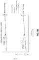
- FIG. 1 schematically depicts a portion of an operational amplifier and three possible approaches for reducing a voltage offset.
- FIG. 2 schematically depicts an operational amplifier according to an embodiment of the present disclosure.
- FIG. 3 is a graph illustrating the variation of transconductance versus temperature for a range of possible proportional to absolute temperature (PTAT) current percentages of the bias current.
- PTAT proportional to absolute temperature
- FIG. 4A is a graph illustrating the voltage offset (V OS ) of the operational amplifier for a range of input voltages (V CM ) before a trimming process.
- FIG. 4B is a graph illustrating the voltage offset (V OS ) of the operational amplifier for a range of input voltages (V CM ) after a trimming process.
- FIG. 6 schematically depicts details of circuit portions for input pair and trimming sources activation and for bias control for constant (ct) current sources of the operational amplifier shown in FIG. 2 .
- FIG. 7 schematically depicts details of circuit portions for input pair activation and bias control for PTAT current sources of the operational amplifier shown in FIG. 2 .
- the present disclosure describes an operational amplifier having two input stages.
- An input of the operational amplifier may be coupled to either of the two input stages.
- the particular input stage that the input is coupled to may be determined based on a comparison of a common-mode input voltage (V CM ) to a threshold (i.e., reference) voltage (V REF ).
- V CM common-mode input voltage
- V REF threshold voltage
- Each input stage includes a pair of transistors arranged as a differential pair (i.e., differential amplifier).
- the first differential pair may include two p-type (i.e., p-channel) metal oxide semiconductor field effect transistors (i.e., pMOS) and may be coupled to the input for a range of relatively low voltages (e.g., V CM ⁇ V REF ).
- the second differential pair may include two n-type (i.e., n-channel) metal oxide semiconductor field effect transistors (i.e., nMOS) and may be coupled to the input for a range of relatively high voltages (e.g., V CM >V REF ).
- Each differential pair is biased by a biasing current at the source terminals of the transistors, which are coupled together.
- the two gate terminals of the selected differential pair are attached to the differential input terminals (IN+, IN ⁇ ) of the operational amplifier.
- the (differential) output of the differential pair is at the drain terminals of the differential pair.
- V OS input offset voltage
- mV millivolt
- ⁇ V microvolt
- Reducing the V OS of an operational amplifier (i.e., opamp) to a voltage in the ⁇ V range may be accomplished by adjusting (i.e., trimming) the current through one of the transistors of the differential pair to compensate for the small differences.
- the trimming may be performed at the time of fabrication (i.e., factory adjusted). For example, each differential pair may be trimmed for a particular input voltage (V CM ) and for a particular temperature (e.g., at 25 degrees Celsius (C)). Because the operation of each transistor in each differential pair varies with temperature, the V OS for each differential pair will have some variation with temperature. This variation is known as the temperature coefficient of the V OS .
- the trimming does not affect (e.g., change) the temperature coefficient (T C ) of the V OS .
- the operational amplifier may accommodate a range of input voltages (V CM ) over which the differential pair changes (i.e., the input pairs function consecutively with respect to V CM ), a V OS with a small overall variation (e.g., around zero volts) with V CM at a particular temperature (e.g., 25 deg. C.) is desirable.
- Trimming an input differential pair of an opamp may be accomplished in different ways. Three approaches are illustrated in FIG. 1 .
- a trim resistor (Rtrim) is used to adjust the bias of the input differential pair of transistors 10 (M 1 , M 2 ). This approach is lossy and the trim resistor could add noise and variation with temperature.
- an auxiliary differential pair 15 (M 1 trim , M 2 trim ) is added to introduce an offset voltage that cancels the V OS of the input differential pair. This approach suffers from complexity and variation.
- the bias current through each transistor (M 1 , M 2 ) is controlled by a current source (Itrim 1 , Itrim 2 ). V OS may be adjusted by adjusting the current difference between the current sources (Itrim 1 , Itrim 2 ).
- the present disclosure describes circuits and methods based on the third approach 3 .
- the disclosure describes circuits and methods to reduce the V OS of an operational amplifier. Additionally, the circuits and methods disclosed accommodate the need to independently adjust the V OS for two input differential pairs (i.e. pMOS and nMOS) that are usually used in rail-to-rail input operational amplifiers.
- FIG. 2 schematically depicts a rail-to-rail operational amplifier according to an embodiment of the present disclosure.
- V CM input voltage
- the first input pair 25 includes pMOS transistors and is used for relatively low V CM .
- the second input pair 30 includes nMOS devices and is used for relatively high V CM .
- a midrange of V CM that is between a relatively low range of V CM and a relatively high range of V CM is defined. In the midrange of V CM , either the first input pair or the second input pair may be used.
- the first input pair 25 and the second input pair 30 each have a V OS that is different and uncorrelated from the other.
- the complementary input pairs 20 can be biased (i.e., turned ON) to function one at a time based on V CM .
- the reason for the input pair selection is to keep the transconductance (gm) of the first gain stage (i.e., the first input pair or the second input pair) of the operational amplifier as constant as possible over the entire V CM range.
- the transition between the first input pair 25 and the second input pair 30 can occur at an input voltage within (e.g., at approximately the middle of) the V CM range where either the first or the second pair functions properly.
- the transition for each pair can be accomplished by using a V CM comparator that compares the input voltage, V CM , to a reference voltage, V REF .
- the constant gm bias control block (i.e., circuit) 35 may include one or more V CM comparators.
- the constant gm bias control circuit 35 may include a first circuit portion having a first comparator 60 corresponding to the constant with temperature portion of the bias current of the input pairs 20 (i.e., Ict_p 61 and Ict_n 71 ). Details of a possible implementation of the first circuit portion are shown in FIG. 6 .
- the constant gm bias control circuit 35 may include a second circuit portion having a second comparator 80 corresponding to the proportional to absolute temperature portion of the bias currents of the input pairs 20 (i.e., Iptat_p 83 and Iptat_n 93 ). Details of a possible implementation of the second circuit portion are shown in FIG. 7 .
- Comparators 60 and 80 have identical inputs (i.e., V REF on one side and V CM on the other) and function in tandem, keeping a constant ratio between PTAT (i.e., ptat) and CT (i.e., ct) portions of the bias currents for the input pairs 20 over the entire input voltage (V CM ) range.
- each complementary input pair is biased with a combination of two currents: one current is proportional to absolute temperature (i.e. ptat) and one current is constant with temperature (i.e., ct).
- the first input pair 25 is biased by a ptat current, Iptat_p, determined by the bias P_ptat voltage and by a constant CT current, Ict_p, determined by the bias_P_ct voltage.
- the second input pair 30 is biased by a ptat current, Iptat_n, determined by the bias_N_ptat voltage and by a constant (CT) current, Ict_n, determined by the bias_N_ct voltage.
- CT constant
- the PTAT currents are subtracted from the signal paths (i.e., out_P ⁇ , out_P+ and out_N ⁇ , out_N+) through a first current source 81 and a second current source 82 (having current determined by a bias_P_ext_ptat voltage) for the first input pair 25 and through a third current source 91 and a fourth current source 92 (having current determined by bias_N_ext_ptat voltage) for the second input pair 30 .
- a first current source 81 and a second current source 82 having current determined by a bias_P_ext_ptat voltage
- bias_N_ext_ptat voltage bias_N_ext_ptat voltage
- All subsequent stages are biased with constant currents only (e.g., the PTAT currents are subtracted from the signal paths to subsequent sections). In this way, the total current of the operational amplifier can have a minimum variation with temperature and the total current consumption can be kept to a minimum.
- each pair can be trimmed with a trim current from a current source.
- the trim current for the first input pair 25 is Itrim_ct_p and the trim current for the second input pair 30 is Itrim_ct_n.
- the trim current for each input pair is constant (i.e., ct) with temperature and can be added to either side (i.e., each transistor) of the input pair to account for both positive and negative offsets.
- the selection of which side to add the current to may be accomplished using switching devices (i.e., switches) 40 .
- T C of a V OS after trimming i.e., T c_trim
- T c_trim trim trim
- each input pair is designed to operate in a subthreshold region.
- each input pair is biased using a bias current (I BIAS ) that is a weighted sum of a PTAT (i.e., temperature dependent) current and a CT (i.e. temperature independent) current to make the transconductance (g m ) for each input pair constant over temperature.
- I BIAS bias current
- g m transconductance
- the input pair may be trimmed using a current source (I TRIM ) that is constant over temperature to obtain a V TRIM that is constant over temperature and that does not affect the T C of V OS .
- I TRIM current source
- I BIAS (i.e., from equation (2)) may be derived from a bandgap-like structure that includes two bipolar transistors and that has an output current equal to ⁇ V BE /R, which can be written as (V T ⁇ ln(z))/R, where z is a multiplication factor between the areas of the emitters of the two bipolar transistors in the bandgap structure.
- the careful control of I BIAS allows for the temperature dependent variable (i.e., the thermal voltage, V T ) to be canceled out of the equation for transconductance (g m ), and what remains is independent of temperature.
- V TRIM can be made constant with temperature by trimming using a current (I TRIM ) that is constant with temperature.
- Trimming can include making the initial V OS offset temperature drift (i.e., temperature coefficient (T C ) as small as possible by biasing an input pair in a weak inversion operating region (i.e. subthreshold region).
- the trimming further includes using a bias current that is predominantly PTAT to make the transconductance of input pair constant with temperature.
- the V OS can be adjusted using a trim current that is constant with temperature to obtain a trimmed V OS that has a thermal coefficient that is relatively unchanged from its initial (i.e., untrimmed) value.
- the first input pair 25 may be biased using a predominantly PTAT sum current (i.e., Iptat_p+Ict_p) and trimmed with a constant trim current, Itrim_ct_p.
- the bias current may be divided in equal parts (i.e., (Iptat_p)/2+(Ict_p)/2) for each transistor in the pair. Further, the current Iptat_p/2 is subtracted from the signal path and Ict_p/2 is passed on to the next amplifier stage.
- the second pair 30 may be biased using a predominantly PTAT sum current (i.e. Iptat_n+Ict_n) and trimmed with a constant trim current, Itrim_ct_n.
- the bias current may be divided in equal parts (i.e., (Iptat_n)/2+(Ict_n)/2) for each transistor in the pair. Further, the current Iptat_n/2 is subtracted from the signal path and Ict_n/2 is passed on to the next amplifier stage.
- I BIAS (m) ⁇ I PTAT +(1 ⁇ m) ⁇ I CONST ).
- FIG. 3 illustrates gm on the y-axis versus temperature on the x-axis for a variety of percentages 45 calculated by Iptat/(I BIAS ) %, where I BIAS is a mathematical combination of I PTAT and I CONST .
- the percentages 45 can vary between approximately 91% and 4% with increasing percentages shown by the arrow in the legend to the right of the graph.
- the variation of gm with temperature may be adjusted.
- a bias current may be determined for which gm is substantially constant over a range of temperatures (e.g., ⁇ 40 to 125 degrees Celsius).
- the transconductance at point P can be approximately 2.05 milli-seimens (mS) at a temperature of approximately 35° C.
- the transconductance can vary between, for example, approximately 1.65 mS (at high temperatures) and approximately 2.55 mS (at low temperatures).
- FIG. 4A is a graph illustrating the voltage offset (V OS ) of the operational amplifier in FIG. 2 for a range of input voltages (V CM ) before trimming.
- the supply voltage is 5.5V.
- the V OS shown in FIG. 4A varies.
- V OS may vary by ⁇ 180 ⁇ V and 650 ⁇ V over a V CM range of 0 to 5.5V.
- V REF reference voltage
- Each of the data lines can be plotted for various temperatures ranging from approximately ⁇ 50 degrees (deg) Celsius (C) to 150 deg C. (as shown in the legend to the right of the graph with increasing temperature being illustrated by the arrow).
- the change in V OS between traces at a particular input voltage (V CM ) is described by the temperature coefficient (T C ) at the particular V CM .
- FIG. 4B is a graph illustrating the voltage offset (V OS ) of the operational amplifier in FIG. 2 for a range of input voltages (V CM ) after trimming.
- V OS voltage offset
- V OS for each input differential pair has been generally reduced (e.g., from approximately 600 ⁇ V to less than 50 ⁇ V), and the trimming reduces the overall variation (i.e., ⁇ V OS > ⁇ V OS_trim ) of V OS over a range (e.g., 0-5.5V) of V CM .
- the data is plotted for various temperatures (e.g., ranging from ⁇ 50 deg C. to 150 deg C.), as shown in the legend to the right of the graph, which corresponds with the legend in FIG. 4A .
- the trimming may correct (i.e., reduced towards zero volts, made approximately zero volts, etc.) a V OS at a particular temperature.
- V OS may be closest to zero for most of the range of input voltages (V CM ) at a particular temperature (e.g., 25 deg C.).
- V CM input voltages
- the trimming for each input differential pair is performed independently and may result in different and unrelated I TRIM values for each.
- the arrangement of the different temperature curves is the same before and after trimming, suggesting that T C is unchanged. This is verified in the following figures.
- FIG. 5A which is based on data from FIGS. 4A and 4B , is a graph illustrating values of the V OS (e.g., ⁇ 160 ⁇ V to 6 ⁇ V for pMOS and ⁇ 65 ⁇ V to 84 ⁇ V for pMOS Trim) for a range of temperatures (e.g., ⁇ 50 to 150 deg C.).
- V DD can be, for example, 5.5V
- V CM can be, for example, 2.8V.
- V OS can be trimmed from about, for example, ⁇ 85 ⁇ V to about ⁇ 6 ⁇ V at 25 deg C.
- Additional linear curve fit lines i.e. Linear (pMOS) and Linear (pMOS) Trim
- pMOS Linear
- pMOS Trim Linear
- the variation (i.e., slope) of V OS versus temperature (i.e., the temperature coefficient) is not significantly changed by the trimming.
- the T C before trimming can be about 0.85 while the T C after trimming can be about 0.77 (i.e., a change that is less than 10%).
- FIG. 5B which is based on data from FIGS. 4A and 4B , is a graph illustrating the V OS (e.g., 584 ⁇ V to 627 ⁇ V for nMOS and ⁇ 32 ⁇ V to 57 ⁇ V for nMOS Trim) for a range of temperatures (i.e., ⁇ 50 to 150 deg C.).
- Vdd can be, for example, 5.5V
- Vcm can be, for example, 4.9V.
- V OS before (i.e., nMOS) and after (i.e., nMOS Trim) a trimming.
- Additional linear curve fit lines i.e. Linear (nMOS) and Linear (nMOS) Trim
- nMOS Linear
- nMOS Trim Linear
- the variation (i.e., slope) of V OS versus temperature (i.e., the temperature coefficient) is not significantly changed by the trimming.
- the T C before trimming can be about 0.24 while the T C after trimming can be about 0.43.
- FIG. 6 schematically depicts details of circuit portions for the input pair and trimming sources activation and for bias control for CT current courses.
- the V CM comparator 60 the pMOS input trim sources 65 and constant bias current source (Ict_p) 61 , the nMOS input trim sources 70 , and the constant bias current source (Ict_n) 71 are shown.
- the pMOS input trim sources 65 and the nMOS input trim sources 70 are included in a trimming circuit for the operational amplifier.
- a first input of the V CM comparator is connected to a reference voltage (V REF ) that is chosen from within a range of possible V CM .
- V REF reference voltage
- a second input of the V CM comparator is made with a pair of MOS devices (P 6 , P 7 ) that are controlled by both inputs of the operational amplifier.
- the same V CM comparator that controls the bias of the input pairs i.e., the portion of the bias that is constant with temperature
- FIGS. 2 and 6 This feature is shown in FIGS. 2 and 6 , where a Pcom node is the bias node for the pMOS input pair and an outP ⁇ node and an out P+ node are nodes used for offset correction of this pair. It can be observed that both the bias current and the trim currents are controlled by the same input of the V CM comparator (i.e., the input driven by the amplifier's inputs).
- the pMOS input trim sources 65 operate as a current source that provides a constant trim current for the pMOS complementary 25 pair, as shown in FIG. 2 (i.e., the current source 65 providing Itrim_ct_p).
- the nMOS input trim sources 70 operate as a current source that provides a constant trim current for the nMOS complementary pair 30 , as shown in FIG. 2 (i.e., the current source 70 providing Itrim_ct_n).
- FIG. 7 schematically depicts details of circuit portions for bias control for PTAT current sources of the operational amplifier shown in FIG. 2 .
- the circuit portions shown in FIG. 7 uses a V CM comparator 80 of the constant gm bias control circuit 35 to steer the PTAT current.
- the PTAT current is significantly higher than the constant current generated by the circuit shown in FIG. 6 , and it will only be used to bias the input pairs, keeping the gm of the devices constant across temperature. This is necessary in order to trim with a constant voltage across temperature and thus limit the degradation of the temperature coefficient of the offset.
- the transistors N 2 and N 5 shown in FIG. 7 , can operate as a current sources, each providing half of current, Iptat_p.
- transistor N 2 when configured as shown in FIG. 7 , can operate as a current source 81 sinking (Iptat_p)/2 from the first input pair 25 .
- transistor N 5 when configured as shown in FIG. 7 , can operate as a current source 82 sinking (Iptat_p)/2 from the first input pair 25 .
- the transistors P 8 and P 10 shown in FIG. 7 , can operate as current sources, each providing half of current, Iptat_n.
- transistor P 8 when configured as shown in FIG. 7 , can operate as a current source 91 sourcing (Iptat_n)/2 to the second input pair 30 .
- transistor P 10 when configured as shown in FIG. 7 , can operate as a current source 92 sourcing (Iptat_n)/2 to the second input pair 30 .
- Some implementations may be implemented using various semiconductor processing and/or packaging techniques. Some implementations may be implemented using various types of semiconductor processing techniques associated with semiconductor substrates including, but not limited to, for example, Silicon (Si), Gallium Arsenide (GaAs), Gallium Nitride (GaN), Silicon Carbide (SiC) and/or so forth.
- semiconductor substrates including, but not limited to, for example, Silicon (Si), Gallium Arsenide (GaAs), Gallium Nitride (GaN), Silicon Carbide (SiC) and/or so forth.
Landscapes
- Engineering & Computer Science (AREA)
- Power Engineering (AREA)
- Amplifiers (AREA)
Abstract
Description
Claims (19)
Priority Applications (2)
| Application Number | Priority Date | Filing Date | Title |
|---|---|---|---|
| US16/530,192 US10924066B2 (en) | 2018-10-11 | 2019-08-02 | Offset voltage trimming for operational amplifiers |
| CN201910956072.6A CN111049486B (en) | 2018-10-11 | 2019-10-10 | Offset voltage trimming for operational amplifiers |
Applications Claiming Priority (2)
| Application Number | Priority Date | Filing Date | Title |
|---|---|---|---|
| US201862744449P | 2018-10-11 | 2018-10-11 | |
| US16/530,192 US10924066B2 (en) | 2018-10-11 | 2019-08-02 | Offset voltage trimming for operational amplifiers |
Publications (2)
| Publication Number | Publication Date |
|---|---|
| US20200119698A1 US20200119698A1 (en) | 2020-04-16 |
| US10924066B2 true US10924066B2 (en) | 2021-02-16 |
Family
ID=70160799
Family Applications (1)
| Application Number | Title | Priority Date | Filing Date |
|---|---|---|---|
| US16/530,192 Active 2039-08-27 US10924066B2 (en) | 2018-10-11 | 2019-08-02 | Offset voltage trimming for operational amplifiers |
Country Status (2)
| Country | Link |
|---|---|
| US (1) | US10924066B2 (en) |
| CN (1) | CN111049486B (en) |
Cited By (2)
| Publication number | Priority date | Publication date | Assignee | Title |
|---|---|---|---|---|
| US11929769B2 (en) | 2021-05-28 | 2024-03-12 | Skyworks Solutions, Inc. | Power amplifier trimming based on coefficients for digital pre-distortion |
| US20250088158A1 (en) * | 2023-09-12 | 2025-03-13 | ZJW Microelectronics North America Inc. | Input stage circuit for an operational amplifier with enhanced input offset voltage trimming capabilities |
Families Citing this family (5)
| Publication number | Priority date | Publication date | Assignee | Title |
|---|---|---|---|---|
| US12328102B2 (en) | 2022-04-28 | 2025-06-10 | Texas Instruments Incorporated | Methods and apparatus to improve performance of amplifiers |
| US20230353096A1 (en) * | 2022-04-28 | 2023-11-02 | Texas Instruments Incorporated | Methods and apparatus to improve performance specifications of amplifiers |
| CN115733447B (en) * | 2022-11-16 | 2024-05-03 | 北京无线电测量研究所 | Rail-to-rail operational amplifier with temperature compensation |
| CN116805859B (en) * | 2023-08-28 | 2023-11-07 | 江苏润石科技有限公司 | Operational amplifier offset voltage regulation circuit and method |
| US20250076442A1 (en) * | 2023-08-31 | 2025-03-06 | Texas Instruments Incorporated | Anisotropic magnetoresistance sensor circuit with adjustable offset trim |
Citations (3)
| Publication number | Priority date | Publication date | Assignee | Title |
|---|---|---|---|---|
| US6614302B2 (en) * | 2001-03-12 | 2003-09-02 | Rohm Co., Ltd. | CMOS operational amplifier circuit |
| US6696894B1 (en) | 2002-06-12 | 2004-02-24 | Analog Devices, Inc. | Operational amplifier with independent input offset trim for high and low common mode input voltages |
| US7170347B1 (en) | 2003-11-17 | 2007-01-30 | National Semiconductor Corporation | Offset trim circuit and method for a constant-transconductance rail-to-rail CMOS input circuit |
Family Cites Families (9)
| Publication number | Priority date | Publication date | Assignee | Title |
|---|---|---|---|---|
| JP2000075942A (en) * | 1998-08-27 | 2000-03-14 | Mitsumi Electric Co Ltd | Offset voltage trimming circuit |
| US6614305B1 (en) * | 2002-02-19 | 2003-09-02 | Texas Instruments Incorporated | Method and circuit for trimming offset and temperature drift for operational amplifiers and voltage references |
| US7109697B1 (en) * | 2005-06-29 | 2006-09-19 | Texas Instruments Incorporated | Temperature-independent amplifier offset trim circuit |
| JP2010283713A (en) * | 2009-06-08 | 2010-12-16 | Sanyo Electric Co Ltd | Offset cancel circuit |
| US8026761B2 (en) * | 2010-01-26 | 2011-09-27 | Microchip Technology Incorporated | Instrumentation amplifier calibration method, system and apparatus |
| US20120139638A1 (en) * | 2010-12-03 | 2012-06-07 | Rambus Inc. | Methods and Circuits for Controlling Amplifier Gain Over Process, Voltage, and Temperature |
| US9246479B2 (en) * | 2014-01-20 | 2016-01-26 | Via Technologies, Inc. | Low-offset bandgap circuit and offset-cancelling circuit therein |
| US9742397B2 (en) * | 2015-11-30 | 2017-08-22 | Silicon Laboratories Inc. | Apparatus for offset correction in electronic circuitry and associated methods |
| IT201700014710A1 (en) * | 2017-02-10 | 2018-08-10 | St Microelectronics Srl | VOLTAGE TRIANGULAR WAVE VOLTAGE GENERATOR AND RELATIVE D-CLASS AMPLIFIER CIRCUIT |
-
2019
- 2019-08-02 US US16/530,192 patent/US10924066B2/en active Active
- 2019-10-10 CN CN201910956072.6A patent/CN111049486B/en active Active
Patent Citations (3)
| Publication number | Priority date | Publication date | Assignee | Title |
|---|---|---|---|---|
| US6614302B2 (en) * | 2001-03-12 | 2003-09-02 | Rohm Co., Ltd. | CMOS operational amplifier circuit |
| US6696894B1 (en) | 2002-06-12 | 2004-02-24 | Analog Devices, Inc. | Operational amplifier with independent input offset trim for high and low common mode input voltages |
| US7170347B1 (en) | 2003-11-17 | 2007-01-30 | National Semiconductor Corporation | Offset trim circuit and method for a constant-transconductance rail-to-rail CMOS input circuit |
Cited By (3)
| Publication number | Priority date | Publication date | Assignee | Title |
|---|---|---|---|---|
| US11929769B2 (en) | 2021-05-28 | 2024-03-12 | Skyworks Solutions, Inc. | Power amplifier trimming based on coefficients for digital pre-distortion |
| US12316357B2 (en) | 2021-05-28 | 2025-05-27 | Skyworks Solutions, Inc. | Power amplifier trimming based on coefficients for digital pre-distortion |
| US20250088158A1 (en) * | 2023-09-12 | 2025-03-13 | ZJW Microelectronics North America Inc. | Input stage circuit for an operational amplifier with enhanced input offset voltage trimming capabilities |
Also Published As
| Publication number | Publication date |
|---|---|
| CN111049486A (en) | 2020-04-21 |
| CN111049486B (en) | 2024-03-01 |
| US20200119698A1 (en) | 2020-04-16 |
Similar Documents
| Publication | Publication Date | Title |
|---|---|---|
| US10924066B2 (en) | Offset voltage trimming for operational amplifiers | |
| US9582021B1 (en) | Bandgap reference circuit with curvature compensation | |
| US9891650B2 (en) | Current generation circuit, and bandgap reference circuit and semiconductor device including the same | |
| US8476967B2 (en) | Constant current circuit and reference voltage circuit | |
| US9310825B2 (en) | Stable voltage reference circuits with compensation for non-negligible input current and methods thereof | |
| US9742397B2 (en) | Apparatus for offset correction in electronic circuitry and associated methods | |
| US8471634B2 (en) | Method and apparatus of common mode compensation for voltage controlled delay circuits | |
| JP4676885B2 (en) | Bias circuit | |
| US20160274617A1 (en) | Bandgap circuit | |
| US7446607B2 (en) | Regulated cascode circuit, an amplifier including the same, and method of regulating a cascode circuit | |
| US10992288B2 (en) | Oscillator device | |
| KR20070019966A (en) | Temperature Compensation Transistor Device and Temperature Compensation Method | |
| US20210286394A1 (en) | Current reference circuit with current mirror devices having dynamic body biasing | |
| US9740232B2 (en) | Current mirror with tunable mirror ratio | |
| US10574200B2 (en) | Transconductance amplifier | |
| US10778148B1 (en) | Gain and sensitivity in a Gilbert switch stage | |
| US7109794B2 (en) | Differential gain stage for low voltage supply | |
| US20030169111A1 (en) | Operational amplifier input stage and method | |
| US7865543B2 (en) | Offset compensation for rail-to-rail avereraging circuit | |
| US20110121888A1 (en) | Leakage current compensation | |
| JP7453562B2 (en) | Differential amplifier circuits, receiving circuits, and semiconductor integrated circuits | |
| JPH0744254A (en) | Cmos constant current source circuit | |
| US20250147536A1 (en) | Voltage reference circuit, integrated circuit, and method for generating a reference voltage | |
| US12547195B2 (en) | Pole frequency tracking in load compensated amplifiers | |
| WO2022170335A1 (en) | Precision operational amplifier with a floating input stage |
Legal Events
| Date | Code | Title | Description |
|---|---|---|---|
| AS | Assignment |
Owner name: SEMICONDUCTOR COMPONENTS INDUSTRIES, LLC, ARIZONA Free format text: ASSIGNMENT OF ASSIGNORS INTEREST;ASSIGNORS:PURDILA, ANCA;PASOI, CONSTANTIN;REEL/FRAME:049942/0811 Effective date: 20190802 |
|
| FEPP | Fee payment procedure |
Free format text: ENTITY STATUS SET TO UNDISCOUNTED (ORIGINAL EVENT CODE: BIG.); ENTITY STATUS OF PATENT OWNER: LARGE ENTITY |
|
| AS | Assignment |
Owner name: DEUTSCHE BANK AG NEW YORK BRANCH, AS COLLATERAL AGENT, NEW YORK Free format text: SECURITY INTEREST;ASSIGNOR:SEMICONDUCTOR COMPONENTS INDUSTRIES, LLC;REEL/FRAME:051145/0062 Effective date: 20191015 |
|
| AS | Assignment |
Owner name: DEUTSCHE BANK AG NEW YORK BRANCH, AS COLLATERAL AGENT, NEW YORK Free format text: CORRECTIVE ASSIGNMENT TO CORRECT THE EXCLUSION OF FAIRCHILD SEMICONDUCTOR CORPORATION OF CONVEYING PARTY PREVIOUSLY RECORDED ON REEL 051145 FRAME 0062. ASSIGNOR(S) HEREBY CONFIRMS THE SECURITY INTEREST;ASSIGNORS:SEMICONDUCTOR COMPONENTS INDUSTRIES, LLC;FAIRCHILD SEMICONDUCTOR CORPORATION;REEL/FRAME:051170/0781 Effective date: 20191015 |
|
| STPP | Information on status: patent application and granting procedure in general |
Free format text: NOTICE OF ALLOWANCE MAILED -- APPLICATION RECEIVED IN OFFICE OF PUBLICATIONS |
|
| STCF | Information on status: patent grant |
Free format text: PATENTED CASE |
|
| AS | Assignment |
Owner name: FAIRCHILD SEMICONDUCTOR CORPORATION, ARIZONA Free format text: RELEASE OF SECURITY INTEREST IN PATENTS RECORDED AT REEL 051145, FRAME 0062;ASSIGNOR:DEUTSCHE BANK AG NEW YORK BRANCH, AS COLLATERAL AGENT;REEL/FRAME:064079/0474 Effective date: 20230622 Owner name: SEMICONDUCTOR COMPONENTS INDUSTRIES, LLC, ARIZONA Free format text: RELEASE OF SECURITY INTEREST IN PATENTS RECORDED AT REEL 051145, FRAME 0062;ASSIGNOR:DEUTSCHE BANK AG NEW YORK BRANCH, AS COLLATERAL AGENT;REEL/FRAME:064079/0474 Effective date: 20230622 |
|
| MAFP | Maintenance fee payment |
Free format text: PAYMENT OF MAINTENANCE FEE, 4TH YEAR, LARGE ENTITY (ORIGINAL EVENT CODE: M1551); ENTITY STATUS OF PATENT OWNER: LARGE ENTITY Year of fee payment: 4 |