US10916396B2 - Load controller and load control method - Google Patents
Load controller and load control method Download PDFInfo
- Publication number
- US10916396B2 US10916396B2 US16/039,420 US201816039420A US10916396B2 US 10916396 B2 US10916396 B2 US 10916396B2 US 201816039420 A US201816039420 A US 201816039420A US 10916396 B2 US10916396 B2 US 10916396B2
- Authority
- US
- United States
- Prior art keywords
- switches
- parallel
- load
- control unit
- current
- Prior art date
- Legal status (The legal status is an assumption and is not a legal conclusion. Google has not performed a legal analysis and makes no representation as to the accuracy of the status listed.)
- Active, expires
Links
Images


Classifications
-
- H—ELECTRICITY
- H01—ELECTRIC ELEMENTS
- H01H—ELECTRIC SWITCHES; RELAYS; SELECTORS; EMERGENCY PROTECTIVE DEVICES
- H01H47/00—Circuit arrangements not adapted to a particular application of the relay and designed to obtain desired operating characteristics or to provide energising current
- H01H47/002—Monitoring or fail-safe circuits
-
- H—ELECTRICITY
- H02—GENERATION; CONVERSION OR DISTRIBUTION OF ELECTRIC POWER
- H02H—EMERGENCY PROTECTIVE CIRCUIT ARRANGEMENTS
- H02H5/00—Emergency protective circuit arrangements for automatic disconnection directly responsive to an undesired change from normal non-electric working conditions with or without subsequent reconnection
- H02H5/04—Emergency protective circuit arrangements for automatic disconnection directly responsive to an undesired change from normal non-electric working conditions with or without subsequent reconnection responsive to abnormal temperature
- H02H5/041—Emergency protective circuit arrangements for automatic disconnection directly responsive to an undesired change from normal non-electric working conditions with or without subsequent reconnection responsive to abnormal temperature additionally responsive to excess current
-
- H—ELECTRICITY
- H03—ELECTRONIC CIRCUITRY
- H03K—PULSE TECHNIQUE
- H03K17/00—Electronic switching or gating, i.e. not by contact-making and –breaking
- H03K17/12—Modifications for increasing the maximum permissible switched current
-
- B—PERFORMING OPERATIONS; TRANSPORTING
- B60—VEHICLES IN GENERAL
- B60R—VEHICLES, VEHICLE FITTINGS, OR VEHICLE PARTS, NOT OTHERWISE PROVIDED FOR
- B60R16/00—Electric or fluid circuits specially adapted for vehicles and not otherwise provided for; Arrangement of elements of electric or fluid circuits specially adapted for vehicles and not otherwise provided for
- B60R16/02—Electric or fluid circuits specially adapted for vehicles and not otherwise provided for; Arrangement of elements of electric or fluid circuits specially adapted for vehicles and not otherwise provided for electric constitutive elements
- B60R16/03—Electric or fluid circuits specially adapted for vehicles and not otherwise provided for; Arrangement of elements of electric or fluid circuits specially adapted for vehicles and not otherwise provided for electric constitutive elements for supply of electrical power to vehicle subsystems or for
-
- G—PHYSICS
- G01—MEASURING; TESTING
- G01K—MEASURING TEMPERATURE; MEASURING QUANTITY OF HEAT; THERMALLY-SENSITIVE ELEMENTS NOT OTHERWISE PROVIDED FOR
- G01K7/00—Measuring temperature based on the use of electric or magnetic elements directly sensitive to heat ; Power supply therefor, e.g. using thermoelectric elements
-
- H—ELECTRICITY
- H02—GENERATION; CONVERSION OR DISTRIBUTION OF ELECTRIC POWER
- H02H—EMERGENCY PROTECTIVE CIRCUIT ARRANGEMENTS
- H02H5/00—Emergency protective circuit arrangements for automatic disconnection directly responsive to an undesired change from normal non-electric working conditions with or without subsequent reconnection
- H02H5/04—Emergency protective circuit arrangements for automatic disconnection directly responsive to an undesired change from normal non-electric working conditions with or without subsequent reconnection responsive to abnormal temperature
- H02H5/047—Emergency protective circuit arrangements for automatic disconnection directly responsive to an undesired change from normal non-electric working conditions with or without subsequent reconnection responsive to abnormal temperature using a temperature responsive switch
-
- H—ELECTRICITY
- H03—ELECTRONIC CIRCUITRY
- H03K—PULSE TECHNIQUE
- H03K17/00—Electronic switching or gating, i.e. not by contact-making and –breaking
- H03K17/08—Modifications for protecting switching circuit against overcurrent or overvoltage
- H03K17/082—Modifications for protecting switching circuit against overcurrent or overvoltage by feedback from the output to the control circuit
-
- H—ELECTRICITY
- H03—ELECTRONIC CIRCUITRY
- H03K—PULSE TECHNIQUE
- H03K17/00—Electronic switching or gating, i.e. not by contact-making and –breaking
- H03K17/08—Modifications for protecting switching circuit against overcurrent or overvoltage
- H03K2017/0806—Modifications for protecting switching circuit against overcurrent or overvoltage against excessive temperature
Definitions
- the present invention relates to a load controller and a load control method.
- a load driving device described in WO 2009/148122 A has been proposed.
- this load driving device one semiconductor relay is directly connected to one load to control power source to the load.
- the current distribution system described in JP 2001-523610 A has been proposed.
- the current distribution system described above has a socket that controls a switch that distributes power source to an actuator. All basic programs necessary for a plurality of sockets are stored in the socket.
- identification numbers are provided in the plurality of sockets, and the socket is configured to select and execute only a basic program corresponding to the identification number out of all the basic programs.
- identification information needs to be set in the socket in order to allow the socket to select a necessary program among all the basic programs. Therefore, there is a problem that work of setting identification information in the socket needs to be done in advance, which is troublesome.
- a power source protective device described in JP 2009-130994 A has been proposed.
- the power source protective device turns off the semiconductor switch in which the upper limit value has been exceeded. Semiconductor switches in which the upper limit value is not exceeded are not turned off.
- a switch through which a high current flows is first turned off due to excess of the current over the upper limit value. Then the current headed for the first turned-off parallel switch is additionally applied to the remaining parallel switch that is still on. Therefore, the remaining parallel switch is also turned off due to the excess over the upper limit value.
- a current including the additional current caused from the previously turned-off parallel switch flows in the subsequently turned-off parallel switch, abnormal heat generation and resistance deterioration cannot be suppressed sufficiently.
- the present invention has been made in view of the above background, and a first object of the present invention is to provide a load controller and a load control method which do not require replacement in response to a change in load.
- a third object of the present invention is to provide a load controller and a load control method capable of suppressing abnormal heat generation and resistance degradation.
- a load controller includes a plurality of switches provided between a power source and a load; a current detection unit configured to detect a current flowing through each of the plurality of switches; and a first adjustment unit configured to adjust number of the switches connected in series to a same load and connected in parallel to each other, based on a detection result of the current detection unit.
- the load controller may further include a plurality of output terminals to which loads are respectively connected; and a switching section configured to switch by arbitrarily selecting a connecting destination of the plurality of switches from among the plurality of output terminals (i.e., select to which output terminals the switches are connected to), wherein the first adjustment unit may control the switching section to adjust the number of the switches.
- the load controller may further include a PWM control unit configured to start a PWM control of the plurality of switches when the current flowing through each of the plurality of switches or sum of currents flowing through the plurality of switches exceeds a threshold value.
- a PWM control unit configured to start a PWM control of the plurality of switches when the current flowing through each of the plurality of switches or sum of currents flowing through the plurality of switches exceeds a threshold value.
- the PWM control unit may output pulses having a same duty to the plurality of parallel-connected switches connected in series to the same load and connected in parallel to each other among the plurality of switches so as to control on/off of the plurality of parallel-connected switches
- the load controller may further include a second adjustment unit configured to shift a phase of the pulses to be output to the plurality of parallel-connected switches such that the currents are constant when the plurality of parallel-connected switches are on.
- the load controller may further include: a PWM control unit configured to output pulses having a same duty to the plurality of parallel-connected switches connected in series to the same load and connected in parallel to each other among the plurality of switches so as to control on/off of the plurality of parallel-connected switches; and a second adjustment unit configured to shift a phase of the pulses to be output to the plurality of parallel-connected switches such that the currents are constant when the plurality of parallel-connected switches are on.
- a PWM control unit configured to output pulses having a same duty to the plurality of parallel-connected switches connected in series to the same load and connected in parallel to each other among the plurality of switches so as to control on/off of the plurality of parallel-connected switches
- a second adjustment unit configured to shift a phase of the pulses to be output to the plurality of parallel-connected switches such that the currents are constant when the plurality of parallel-connected switches are on.
- a method for controlling a load includes detecting a current flowing through each of a plurality of switches provided between a power source and a load; and adjusting number of the switches connected in series to a same load and connected in parallel to each other according to a detection result.
- a control system includes a load control unit that controls power source to a load, and an execution unit that causes the load control unit to execute only a program corresponding to the load control unit among a plurality of programs, and the load control unit detects a current flowing in the load, and the execution unit selects a program corresponding to a current value detected by the load control unit or corresponding to a value related to the current value out of the plurality of programs and causes the load control unit to execute the program.
- the load control unit may detect a voltage applied to the load, and the execution unit may select a program corresponding to the power consumption obtained from the detected current value and voltage value.
- the execution unit may include a writing device that writes a program in the load control unit, and the writing device may write the selected program to the load control unit.
- the load control unit may be connected to a wire harness having a connector attached to its one end, and the writing device may be connected to the connector.
- a writing device for writing a program in a load control unit that controls power source to a load is characterized by having a receiving unit that receives a current value of the current flowing in the load control unit, and a writing unit that selects a program corresponding to the received current value or corresponding to the value related to the received current value among the plurality of programs and writes the selected program in the load control unit.
- a load controller is characterized by having a plurality of parallel switches connected in series to the same load and connected in parallel to each other and turning on and off power supply to the same load, an abnormality detection unit that detects abnormality of each of the plurality of parallel switches, and a control unit that turns off all of the plurality of parallel switches when an abnormality is detected in any one of the plurality of parallel switches.
- the abnormality detection unit may detect the abnormality if even one of the temperature of the parallel switch, the current flowing through the parallel switch, and the power supplied to the parallel switch is equal to or higher than a threshold value.
- a load control method is characterized by having steps of detecting an abnormality in each of a plurality of parallel switches connected in series to the same load and connected in parallel to each other and turning on and off power supply to the same load, and turning off all of the plurality of parallel switches when an abnormality is detected in any one of the plurality of parallel switches.
- the number of switches connected in parallel can be increased to cope with the change. Therefore, it is unnecessary to change the switch to one allowing a high current, so that no replacement is necessary.
- FIG. 1 is a diagram showing a first embodiment of a load controller of the present invention
- FIG. 2 is a flowchart showing a selection processing procedure of a microcomputer shown in FIG. 2 ;
- FIG. 3 is a diagram in which a writing device is connected to the load controller shown in FIG. 1 ;
- FIG. 4 is an explanatory diagram for describing an operation in the selection processing of the microcomputer shown in FIG. 1 ;
- FIG. 5 is an explanatory diagram for describing the operation in the selection processing of the microcomputer shown in FIG. 1 ;
- FIG. 6 is an explanatory diagram for describing the operation in the selection processing of the microcomputer shown in FIG. 1 ;
- FIG. 7 is a time chart of currents when a semiconductor relay fails
- FIG. 8 is a flowchart showing a first overcurrent suppression processing of the microcomputer shown in FIG. 1 ;
- FIG. 9 is a time chart of the currents when the power source voltage increases.
- FIG. 10 is a flowchart showing a second overcurrent suppression processing of the microcomputer shown in FIG. 1 ;
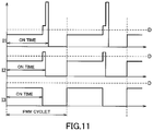
- FIG. 11 is a time chart of the currents when the off-timings of semiconductor relays are deviated
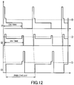
- FIG. 12 is a time chart of the currents when on/off timings of the semiconductor relays are deviated
- FIG. 13 is a time chart of the currents when on/off timings of the semiconductor relays accord with each other;
- FIG. 14 is a diagram showing a second embodiment of a writing system as a control system of the present invention.
- FIG. 15 is a diagram showing a state in which the load control unit shown in FIG. 14 is attached to a wire harness;
- FIG. 16 is a block diagram showing a configuration of a load control unit shown in FIG. 14 ;
- FIG. 17 is a flowchart showing a processing procedure of the load control unit and the writing device shown in FIG. 14 ;
- FIG. 18 is a diagram showing an embodiment of a load controller of the present invention.
- FIG. 19 is a diagram showing details of an IPD shown in FIG. 18 ;
- FIG. 20 is a functional block diagram of a control unit shown in FIG. 18 ;
- FIG. 21 is a flowchart showing a protection processing procedure of the control unit shown in FIG. 18 ;
- FIG. 22 is a time chart of the heat quantity of each of the semiconductor relays connected in parallel in the conventional example
- FIG. 23 is a time chart of the heat quantity of each of the parallel-connected semiconductor relays in the present embodiment shown in FIG. 18 ;
- FIG. 24 is a diagram showing a state in which a writing device is connected to the load controller shown in FIG. 18 ;
- FIG. 25 is an exemplary reference table for the writing system of FIG. 14 .
- FIG. 1 is a diagram showing the first embodiment of the load controller according to the present invention.
- a load controller 1 of the present invention is a device that controls power supply to a load such as a lamp mounted on a vehicle, namely a passenger car for example.
- the load controller 1 is provided with a power source terminal T 1 , a ground terminal T 2 , a communication terminal T 3 and a plurality of output terminals T 41 to T 44 which are constituted by terminal fittings. Further, the load controller 1 includes semiconductor relays CH 1 to CH 4 as a plurality of switches, a switching unit 11 as the switching section, a power source IC 12 , a communication IC 13 , a microcomputer 14 .
- the semiconductor relays CH 1 to CH 4 may be simply referred to as semiconductor relays CH.
- the present invention is not limited to this.
- the number of the semiconductor relays CH may be two or more.
- the power source terminal T 1 is a terminal to which power is supplied.
- the ground terminal T 2 is a terminal to which a ground is supplied.
- the communication terminal T 3 is a terminal through which a communication signal is input/output.
- the plurality of output terminals T 41 to T 44 are connected to loads 31 and 32 (hereinafter also simply referred to as “loads 3 ”) and are terminals for power output.
- the power source terminal T 1 and the plurality of output terminals T 41 to T 44 are connected by a power source line L 1 .
- the power source line L 1 has a plurality of branches on the output terminal T 41 to T 44 side.
- the plurality of semiconductor relays CH 1 to CH 4 are respectively provided on branch lines L 11 to L 14 branched from the power source line L 1 .
- the semiconductor relays CH 1 to CH 4 are turned on, power is output from the connected output terminals T 41 to T 44 and is supplied to the loads 31 and 32 connected to the output terminals T 41 to T 44 .
- each of the semiconductor relays CH 1 to CH 4 has a function as a current detection unit.
- the semiconductor relays CH 1 to CH 4 detect currents flowing in themselves and output the detected currents to the microcomputer 14 .
- the switching unit 11 is provided between the plurality of semiconductor relays CH 1 to CH 4 and the plurality of output terminals T 41 to T 44 .
- the switching unit 11 is composed of a switch (not shown), and a connecting destination of the plurality of semiconductor relays CH 1 to CH 4 can be arbitrarily selected and switched from among the plurality of output terminals T 41 to T 44 .
- the power source IC 12 converts the power supply input from the power source terminal T 1 and the ground terminal T 2 into the operation power supply of the microcomputer 14 and supplies the converted power supply to the microcomputer 14 .
- the communication IC 13 is an IC for communicating with a device (master ECU, another load controller, writing device, etc.) having another communication function provided outside the load controller 1 .
- the microcomputer 14 is configured to include a central processing unit (CPU) having memories such as a random access memory (RAM) and a read only memory (ROM), and controls the entire load controller 1 .
- CPU central processing unit
- RAM random access memory
- ROM read only memory
- the microcomputer 14 is connected to each of the semiconductor relays CH 1 to CH 4 and controls the power supply to a load 3 owing to communication with the master ECU and by turning on and off the semiconductor relays CH 1 to CH 4 . Further, the microcomputer 14 is connected to the switching unit 11 , and controls the switching unit 11 based on currents flowing through the semiconductor relays CH 1 to CH 4 .
- FIG. 2 is a flowchart showing a selection processing procedure of the microcomputer 14 that selects the connecting destination of the semiconductor relays CH 1 to CH 4 from among the plurality of output terminals T 41 to T 44 .
- the microcomputer 14 functions as a first adjustment unit.
- the microcomputer 14 executes selection processing shown in FIG. 2 .
- the user implements change (including addition) of the loads 31 and 32 connected to the load controller 1 , and then connects the writing device 2 to the load controller 1 . This is done for the purpose of writing a control program for the changed loads 31 and 32 in the load controller 1 .
- the microcomputer 14 controls the switching unit 11 to connect the output terminals T 41 to T 44 and the semiconductor relays CH 1 to CH 4 on a one to one basis (step S 1 ) as shown in FIG. 4 .
- the microcomputer 14 takes in currents I 1 to I 4 detected by the respective semiconductor relays CH 1 to CH 4 (step S 2 ) and determines whether any one current exceeding a threshold value A among the current I 1 to I 4 is present (step S 3 ).
- step S 3 When none of the currents I 1 to I 4 exceeding the threshold value A is present (N in step S 3 ), the microcomputer 14 transmits a message to the writing device 2 that the connection has been normally performed (step S 4 ), and terminates the processing.
- the writing device 2 Upon receiving the message that the connection has been performed normally, the writing device 2 transmits the control program of the connected load 3 to the load controller 1 .
- the load controller 1 writes the transmitted control program in a memory such as a ROM.
- step S 3 when any one of the currents I 1 to I 4 exceeding the threshold value A is present (Y in step S 3 ), the microcomputer 14 determines whether there is a current value 0 among the currents I 1 to I 4 (step S 5 ). When there is no current value 0 (N in step S 5 ), the microcomputer 14 determines that there is no semiconductor relay CH to which the load 3 is not connected, and transmits information on a connection error of the load 3 to the writing device 2 (step S 6 ), then ending the processing.
- step S 5 When there is a current value 0 (Y in step S 5 ), the microcomputer 14 controls the switching unit 11 so that one of the semiconductor relays CH having no current flow is connected to the output terminals T 41 to T 44 connected with the semiconductor relay CH through which a current exceeding the threshold value A flows (step S 7 ), and returns the processing to step S 2 .
- the microcomputer 14 transmits a message to the writing device 2 that the connection is normal in the state shown in FIG. 4 .
- the microcomputer 14 connects the semiconductor relay CH 3 to the output terminal T 42 so as to connect the semiconductor relay CH 3 to the semiconductor relay CH 2 in parallel (step S 7 ).
- the semiconductor relay CH 3 is one of the semiconductor relays CH in which no current was flowing (no load was connected). As a result, the current flowing through the load 32 branches to the semiconductor relays CH 2 and CH 3 , so that the current I 2 decreases.
- the microcomputer 14 transmits a message that the connection is normal to the writing device 2 in the state shown in FIG. 5 .
- the microcomputer 14 connects the semiconductor relay CH 4 to the output terminal T 42 and connect the relay in parallel to the semiconductor relays CH 2 and CH 3 as shown in FIG. 6 (step S 7 ).
- the microcomputer 14 transmits a message that the connection is normal to the writing device 2 in the state shown in FIG. 6 .
- the microcomputer 14 can adjust the number of semiconductor relays CH 1 to CH 4 connected to the same load 32 in series and connected to each other in parallel, in accordance with the detection results of the semiconductor relays CH 1 to CH 4 as shown in FIGS. 4 to 6 .
- the number of semiconductor relays CH 1 to CH 4 connected in parallel is increased by utilizing the semiconductor relays CH 3 and CH 4 to which the load 32 is not connected so that the microcomputer 14 can cope with the situation. Therefore, it is unnecessary to change the semiconductor relays CH 1 to CH 4 (i.e., the load controller 1 ) themselves to those allowing a high current.
- the switching unit 11 can arbitrarily select the connecting destinations of the plurality of semiconductor relays CH 1 to CH 4 for switching from among the plurality of output terminals T 41 to T 44 . Then, the microcomputer 14 controls the switching unit 11 to adjust the number of semiconductor relays CH 1 to CH 4 connected in parallel. Thereby, the number of semiconductor relays CH 1 to CH 4 connected in parallel can be adjusted with a simple configuration.
- the first overcurrent suppression processing and the second overcurrent suppression processing of the above-described load controller 1 will be described with reference to FIGS. 7 to 10 .
- the user connects the master ECU mounted on the vehicle to the communication terminal T 3 .
- the microcomputer 14 operates according to the written control program and turns on and off the semiconductor relays CH 1 to CH 4 according to an on/off command from the master ECU. In the normal state, the microcomputer 14 always keeps the semiconductor relays CH 1 to CH 4 on when receiving the on-command.
- the microcomputer 14 executes the first overcurrent suppression processing and the second overcurrent suppression processing in parallel.
- the microcomputer 14 functions as a PWM control unit, and switches from the always-on state of the semiconductor relays CH 1 to CH 4 to the PWM control that outputs pulses with a constant cycle according to the on-command.
- the semiconductor relays CH 1 to CH 3 are now assumed to be connected to the same load 3 (the same output terminal among T 41 to T 44 ) and to be connected in parallel with each other. Further, it is assumed that another semiconductor relay is not connected to the semiconductor relay CH 4 in parallel.
- the microcomputer 14 takes in the currents I 1 to I 4 detected by the respective semiconductor relays CH 1 to CH 4 (step S 10 ) and determines whether any one of the currents I 1 to I 4 exceeding a threshold value B is present (step S 11 ). While none of the currents I 1 to I 4 exceeds the threshold value B (N in step S 11 ), the microcomputer 14 returns to step S 10 and the always-on control is continued.
- the microcomputer 14 determines whether the semiconductor relays CH 1 to CH 4 through which the currents I 1 to I 4 exceeding the threshold value B flows are the parallel-connected semiconductor relays (step S 12 ).
- the “parallel-connected semiconductor relays” refers to ones constituting a plurality of semiconductor relays connected to the same load 3 and connected in parallel with each other. As shown in FIG. 7 , when the semiconductor relay CH 3 breaks down, the currents I 2 and I 3 flowing through the semiconductor relays CH 1 and CH 2 exceed the threshold value B. Since the semiconductor relays CH 2 and CH 3 are connected in parallel, the microcomputer 14 determines that the relays are parallel-connected semiconductor relays in step S 12 (Y in step S 12 ).
- the microcomputer 14 calculates the average value or the maximum value of the currents I 1 to I 3 of the parallel-connected semiconductor relays CH 1 to CH 3 (step S 13 ).
- the microcomputer 14 calculates the on-duty of the semiconductor relays CH 1 to CH 3 so that the currents I 1 to I 3 will be equal to or less than the threshold value B (step S 14 ).
- the microcomputer 14 starts the PWM control to turn on/off the parallel-connected semiconductor relays CH 1 to CH 3 with the duty calculated in step S 14 (step S 15 ), and ends the processing.
- the microcomputer 14 determines that the relays are not parallel-connected semiconductor relays in step S 12 (N in step S 12 ). Thereafter, the microcomputer 14 calculates the on-duty of the semiconductor relay CH 4 so that the current I 4 is equal to or less than the threshold value B (step S 16 ). Thereafter, the microcomputer 14 starts PWM control for turning on and off the semiconductor relay CH 4 with the duty calculated in step S 16 (step S 17 ), and ends the processing.
- the microcomputer 19 takes in the currents I 1 to I 4 detected by the respective semiconductor relays CH 1 to CH 4 (step S 20 ) and then calculates the sum of the currents I 1 to I 4 (step S 21 ). When the calculated sum is equal to or less than a threshold value C (N in step S 22 ), the microcomputer 19 returns to step S 20 again.
- step S 22 when the sum exceeds the threshold value C (Y in step S 22 ), the microcomputer 14 calculates the on-duty of all the semiconductor relays CH 1 to CH 4 in which the sum will not exceed the threshold value C (step S 23 ). Thereafter, the microcomputer 14 starts the PWM control for turning on and off all the semiconductor relays CH 1 to CH 4 with the duty calculated in step S 23 (step S 24 ), and ends the processing.
- the semiconductor relays CH 1 to CH 4 are switched from always-on state to PWM control state, and the currents I 1 to I 4 decrease, so that the sum does not exceed the threshold value C as shown in FIG. 9 . This can inhibit overcurrent from flowing through the semiconductor relays CH 1 to CH 4 .
- the microcomputer 14 simultaneously outputs pulses of the same duty to the semiconductor relays CH connected to the same load 3 and connected in parallel to turn the relays on and off.
- the semiconductor relays CH 1 to CH 3 cannot be turned on and off at the same time due to their different characteristics.
- the timing for the turning-off may be delayed in the order of the semiconductor relays CH 3 , CH 2 , and CH 1 . In this case, a large current is allowed to flow through the semiconductor relay CH 1 that has been turned off last at every cycle of the PWM control.
- the timing for turning-on may be delayed in the order of the semiconductor relays CH 1 , CH 2 , and CH 3 . In this case, a large current is allowed to flow also through the semiconductor relay CH 1 which is turned on first at every cycle of the PWM control.
- the microcomputer 14 when executing the PWM control, the microcomputer 14 functions as a second adjustment unit, and deviates the phases of the on/off signals output to the parallel-connected semiconductor relays CH 1 to CH 3 from each other, thereby enabling the semiconductor relays CH 1 to CH 3 to be turned on and off at the same time.
- the microcomputer 14 detects currents flowing through the semiconductor relays CH 1 to CH 3 .
- the microcomputer 14 delays the on-signals to the semiconductor relays CH 1 and CH 2 through which the currents I 1 and I 2 exceeding a threshold value D flow at the timing of on by a predetermined phase for example, with respect to an on-signal to the semiconductor relay CH 3 through which the current I 3 equal to or less than the threshold value D flows.
- the microcomputer 14 repeatedly performs this operation until the currents I 1 to I 3 at the on-timing become equal to or less than the threshold value D.
- the microcomputer 14 advances, the off-signals to the semiconductor relays CH 1 and CH 2 through which the currents I 1 and I 2 exceeding the threshold value D flow at the timing of off by a predetermined phase with respect to the off-signal to the semiconductor relay CH 3 through which the current I 3 equal to or less than the threshold value D flows.
- the microcomputer 14 repeatedly performs this operation until the currents I 1 to I 3 at the off-timing all become equal to or less than the threshold value.
- the microcomputer 14 can turn on and off the semiconductor relays CH 1 to CH 3 at the same time as shown in FIG. 13 .
- the microcomputer 14 shifts the phases of the pulses output to the parallel-connected semiconductor relays CH 1 to CH 3 so that the currents I 1 to I 3 when the parallel-connected semiconductor relays CH 1 to CH 3 are on become constant. This can suppress the overcurrent caused by the on/off time lag of the semiconductor relays CH 1 to CH 3 .
- the microcomputer 14 when the currents I 1 to I 4 flowing through the semiconductor relays CH 1 to CH 4 exceed the threshold value B or the sum of the currents I 1 to I 4 exceeds the threshold value C, the microcomputer 14 switches from the always-on state to PWM control state, but the manner is not limited to this.
- the microcomputer 14 may always perform PWM control so as to reset the duty when the currents I 1 to I 4 flowing through the semiconductor relays CH 1 to CH 4 exceed the threshold value B or the sum of the currents I 1 to I 4 exceeds the threshold value C.
- the semiconductor relays CH 1 to CH 4 are provided with the current detection function, but the manner is not limited thereto.
- a current detection unit for detecting the currents I 1 to I 4 may be provided separately from the semiconductor relays CH 1 to CH 4 .
- the number of the semiconductor relays CH 1 to CH 4 is equal to the number of the output terminals T 41 to T 44 , but the number is not limited thereto.
- the number of the semiconductor relays CH 1 to CH 4 may be larger than the number of the output terminals T 41 to T 44 .
- FIG. 14 is a diagram showing an embodiment of a writing system as a control system of the present invention.
- FIG. 15 is a diagram showing a state in which the load control unit shown in FIG. 14 is attached to the wire harness.
- FIG. 16 is a block diagram showing the configuration of the load control unit shown in FIG. 14 .
- FIG. 25 shows an exemplary reference table for the writing system.
- a writing system 100 of the present invention is a system for writing a program in a load control unit 110 that controls a load 102 mounted on a vehicle such as a passenger car.
- the plurality of load control units 110 are connected by bus-connection using a wire harness 103 composed of a communication line L 101 , ground line L 102 and power source line L 103 .
- the plurality of load control units 110 are communicably connected to each other by the above-mentioned communication line L 101 .
- a connector 104 is attached to an end of the wire harness 103 described above.
- the connector 104 is constituted by terminal fittings attached to the ends of the communication line L 101 , the ground line L 102 and the power source line L 103 , and a housing accommodating these terminal fittings (none of which are shown). Not only a connector attached to an electric junction box mounted on the vehicle, an end of another wire harness, or the like, but also the writing device 120 can be detachably connected to the connector 104 .
- the plurality of load control units 110 include a power source terminal T 101 , an input/output terminal T 102 , a plurality of output terminals T 31 to T 3 n , a plurality of switches SW 1 to SWn, a power source IC 111 , and a microcomputer 112 .
- the power source terminal T 101 is a terminal to which the power source line L 103 is connected and to which power from a battery 105 is input.
- the input/output terminal T 102 is a terminal to which the communication line L 101 is connected and through which a communication signal is input or output.
- the plurality of output terminals T 31 to T 3 n are terminals connected to the load 102 and through which power is output.
- the above-described power source terminal T 101 and the plurality of output terminals T 31 to T 3 n are connected by a power source line L 104 .
- the power source line L 104 are branched into a plurality of branch lines L 1041 to L 104 n , which are connected to the plurality of output terminals T 31 to T 3 n , respectively.
- the power input from the power source terminal T 101 is distributed so as to be output from the plurality of output terminals T 31 to T 3 n.
- the plurality of switches SW 1 to SWn are provided corresponding to the output terminals T 31 to T 3 n , respectively, and are provided on the branch lines L 1041 to L 104 n branched from the power source line L 104 , respectively.
- the switches SW 1 to SWn are turned on, power is output from the corresponding output terminals T 31 to T 3 n , and is supplied to the load 102 .
- the switches SW 1 to SWn are turned off, the power supply from the corresponding output terminals T 31 to T 3 n is interrupted, and power supply to the load 102 is cut off.
- Each of the switches SW 1 to SWn is provided with a current detection function for detecting a current flowing through the switches SW 1 to SWn themselves, and outputs the detected current value to the microcomputer 112 .
- the total value of the currents flowing through the switches SW 1 to SWn is the current flowing in the load control unit 110 .
- the power source IC 111 converts the power supply input from the power source terminal T 101 to the operation power supply for the microcomputer 112 and outputs the operation power supply to the microcomputer 112 .
- the microcomputer 112 has an operating section 112 A, a voltage detecting section 112 B, an input/output section 112 C, a receiving section 112 D, a storage section 112 E, and an output section 112 F.
- the operating section 112 A is constituted by a central processing unit (CPU), and controls the entire load control unit 110 .
- the voltage detecting section 112 B detects a voltage to be applied to the load control unit 110 .
- the input/output section 112 C inputs and outputs signals transmitted and received via the communication line L 101 .
- the receiving section 112 D is connected to the plurality of switches SW 1 to SWn respectively, and receives the current value detected by the switches SW 1 to SWn, thereby outputting the current value to the operating section 112 A.
- the storage section 112 E stores a program to be executed by the operating section 112 A, and is a memory in which writing/rewriting of the programs are possible.
- the output section 112 F is connected to the operating section 112 A, and outputs on/off signals of the plurality of switches SW 1 to SWn.
- the above-described operating section 112 A transmits the current value detected by the switches SW 1 to SWn and the voltage value detected by the voltage detecting section 112 B to the writing device 120 .
- the writing device 120 is configured to include a CPU provided with a memory such as a RAM and a ROM, for example. Upon receiving the current value and the voltage value from the load control unit 110 , the writing device 120 calculates the power consumption, selects a program corresponding to the power consumption, and writes the program in the load control unit 110 . The writing device 120 selects a program with reference to the table shown in FIG. 25 stored in the ROM, for example.
- the “all switches off” shown in FIG. 25 is a program for the always-off control for all the switches SW 1 to SWn. This all switches off is a program necessary for the load control unit 110 connected with no load 102 (that is, the power consumption is 0). In addition, the all switches off is a program which is not necessary for the load control unit 110 connected with the load 102 (that is, the power consumption is larger than 0).
- the “on/off of switch” is a program for controlling on/off of the switches SW 1 to SWn.
- the on/off of switch is a program necessary for the load control unit 110 , which is connected to the load 102 and which requires on/off control of the switches SW 1 to SWn.
- the on/off of switch is a program which is not necessary for the load control unit 110 , which is not connected with any load 102 and does not require on/off control of the switches SW 1 to SWn.
- the allowable current that can pass through the load control unit 110 is determined by the capacities of the switches SW 1 to SWn, the thickness of the power source line L 103 connected to the load control unit 110 , and the like.
- the power saving controls A, B, . . . shown in FIG. 25 are programs for controlling so that no current higher than the allowable current flows in the load control unit 110 .
- the program is one for performing control such as decreasing the duty ratio when the current is likely to exceed the allowable current in the case of driving the load 102 by the PWM method.
- the power saving controls A, B, . . . are necessary programs for the load control unit 110 connected with the load 102 consuming high power (for example, the load 102 whose power consumption is the threshold value or more). Further, the power saving controls A, B, are programs which are not necessary for the load control unit 110 connected with the load 102 consuming low power (for example, the load 102 whose power consumption is less than the threshold value).
- the power saving controls A, B, . . . are, for example, programs having different parameters. These parameters are determined according to the power consumption of the load control unit 110 .
- Writing of the program in the present embodiment may be performed before mounting of the load control unit 110 in the vehicle or may be performed after the mounting.
- the user Before mounting the unit on the vehicle, the user connects the dummy load 102 to the output terminals T 31 to T 3 n of the load control unit 110 .
- the dummy load 102 is the same as the load 102 mounted on the vehicle.
- the actual load 102 mounted on the vehicle is already connected to the output terminals T 31 to T 3 n of the load control unit 110 .
- the user connects the writing device 120 to the connector 104 of the wire harness 103 . Due to this, power is supplied from the battery 105 of the writing device 120 to each load control unit 110 .
- the writing device 120 and the load control unit 110 start the writing processing shown in FIG. 17 .
- each load control unit 110 transmits a writing request in the writing processing (step S 110 ).
- the writing request from the load control unit 110 cannot be received within a predetermined time T 11 after executing the writing processing (N in step S 120 )
- the writing device 120 displays a connection error (step S 129 ) and ends the writing processing.
- the writing device 120 upon receiving a writing request from each load control unit 110 within the predetermined time T 11 (Y in step S 120 ), the writing device 120 transmits a command for transmission of a current value and a voltage value to each load control unit 110 (step S 121 ).
- the load control unit 110 Upon receiving the transmission command (Y in step S 111 ), the load control unit 110 turns on all the switches SW 1 to SWn (step S 112 ) and supplies power to all the loads 102 connected to the output terminals T 31 to T 3 n . Thereafter, the load control unit 110 takes in the current value detected by each of the switches SW 1 to SWn and also takes in the voltage value detected by the voltage detecting section 112 B (step S 113 ). Next, the load control unit 110 transmits the captured current value and voltage value to the writing device 120 (step S 114 ).
- the writing device 120 Upon receiving the current value and the voltage value from the load control unit 110 by functioning as a receiving section (Y in step S 122 ), the writing device 120 adds the current values of the switches SW 1 to SWn thereto to obtain the value of the current that flows in the load control unit 110 . Thereafter, the writing device 120 calculates the power consumption by multiplying the obtained current value and the received voltage value together (step S 123 ). Then, the writing device 120 selects a program corresponding to the magnitude of the power consumption with reference to FIG. 25 (step S 124 ).
- the writing device 120 functions as a writing unit and transmits the program selected in step S 124 to the load control unit 110 (step S 125 ).
- the load control unit 110 Upon receiving a program from the writing device 120 (Y in step S 115 ), the load control unit 110 writes the received program (step S 116 ).
- the load control unit 110 transmits a success signal indicating the success (step S 118 ), and terminates the processing.
- the load control unit 110 immediately terminates the processing.
- the writing device 120 When the writing device 120 cannot receive the success signal within a predetermined time T 12 after transmitting the program (N in step S 126 ), the writing device 120 displays the failure (step S 127 ) and ends the processing. On the other hand, when the writing device 120 receives the success signal within the predetermined time T 12 after transmitting the program (Y in step S 126 ), the writing device 120 displays success of the writing (step S 128 ) and ends the processing.
- the writing device 120 selects a program corresponding to the power consumption of the load control unit 110 among a plurality of programs, and writes the selected program in the load control unit 110 . Due to this, no work for setting the identification number to the load control unit 110 in advance is required, so that the program can be easily selected.
- the plurality of load control units 110 are connected to the wire harness 103 to which the connector 104 is attached at one end thereof, and the writing device 120 is connected to the connector 104 .
- the program can be written in the load control unit 110 in a state in which the plurality of load control units 110 are attached to the wire harness 103 .
- programs can be easily written in the plurality of load control units 110 .
- the execution unit is composed of the writing device 120 , which selects the program according to the power consumption for writing, but the present invention is not limited thereto.
- the load control unit 110 functions as a load control unit and an execution unit.
- power consumption is used as a value corresponding to the current value, but the manner is not limited thereto.
- a program corresponding to the current value may be selected by detecting only the current value.
- the load control unit 110 performs writing by the writing device 120 in a state of being attached to the wire harness 103 , but the manner is not limited thereto.
- the writing may be performed by connecting the writing device 120 and the power supply to the load control unit 110 before the attachment of the wire harness 103 .
- the load control unit 110 transmits each current value detected by the switches SW 1 to SWn and the voltage value detected by the voltage detecting section 112 B, and the writing device 120 adds up each current values and obtains the power consumption by multiplying the value by the voltage value, but the manner is not limited thereto.
- the load control unit 110 may add up respective current values detected by the switches SW 1 to SWn to transmit the added current value to the writing device 120 .
- the load control unit 110 adds up respective current values detected by the switches SW 1 to SWn, and may multiply the value by the voltage value detected by the voltage detecting section 112 B to obtain power consumption, thereby transmitting the obtained power consumption to the writing device 120 .
- FIG. 18 is a diagram showing one embodiment of the load controller of the present invention.
- a load controller 201 of the present invention is a device that controls power supply to loads 21 and 22 such as lamps mounted in a vehicle, namely a passenger car for example.
- the load controller 201 includes a power source terminal T 201 , a communication terminal T 202 , and a plurality of output terminals T 301 and T 302 constituted by terminal fittings. Further, the load controller 201 includes a plurality of intelligent power devices (IPDs) 211 and 212 , a switching section 213 , and a control unit 214 .
- IPDs intelligent power devices
- the power source terminal T 201 is a terminal to which the power source circuit 203 is connected and to which power is supplied.
- the communication terminal T 202 is a terminal to which the communication circuit 204 is connected for input and output of a communication signal.
- the plurality of output terminals T 301 and T 302 are connected to the loads 21 and 22 , respectively for outputting power.
- the IPDs 211 and 212 have power source terminals T 401 and T 402 (see FIG. 19 ), a plurality of semiconductor relays CH 11 to CH 14 , CH 21 to CH 24 (hereinafter also simply referred to as “semiconductor relays CH”), and a plurality of relay terminals T 511 to T 514 , T 521 to T 524 , input terminals T 61 and T 62 , and sense terminals T 71 and T 72 .
- the power source terminals T 401 and T 402 are terminals to which the power supplied from the power source terminal T 201 is distributed and input.
- the power supplied from the power source terminals T 401 and T 402 is distributed to the plurality of semiconductor relays CH.
- the present invention is not limited to this.
- the number of the semiconductor relays may be two or more.
- Each semiconductor relay CH has a function as a current detection unit.
- the semiconductor relay CH detects the current flowing through itself and outputs the detected current data to the control unit 214 .
- the sense terminals T 71 and T 72 are terminals for outputting the current data respectively detected by the respective semiconductor relays CH.
- the switching section 213 is provided between the IPDs 211 and 212 and the output terminals T 301 and T 302 .
- the switching section 213 is composed of switches (not shown), and the connecting destinations of a plurality of semiconductor relays CH can be arbitrarily selected for switching from the output terminals T 301 and T 302 .
- Control of the switching section 213 is performed by the control unit 214 .
- the control unit 219 adjusts the number of switches connected to the same loads 21 and 22 and connected in parallel to each other so that the current flowing through each of the semiconductor relays CH does not exceed a threshold value when the loads 21 and 22 are changed.
- FIG. 18 shows an example in which the semiconductor relays CH 11 and CH 19 of the IPD 211 and the semiconductor relays CH 21 and CH 24 of the IPD 212 are connected to the output terminal T 301 by the control unit 219 . Because of this, when the semiconductor relays CH 11 , CH 14 , CH 21 , and CH 24 are turned on, power is output from the output terminal T 301 and is supplied to the load 21 connected to the output terminal T 301 . When the semiconductor relays CH 11 , CH 14 , CH 21 , and CH 24 are turned off, the power supply from the output terminal T 301 is cut off, and the power supply to the load 21 connected to the output terminal T 301 is cut off.
- These semiconductor relays CH 11 and CH 14 of the IPD 211 and the semiconductor relays CH 21 and CH 24 of the IPD 212 are a plurality of parallel semiconductor relays (parallel switches) connected to the same load 21 and connected in parallel with each other.
- the semiconductor relays CH 12 and CH 13 of the IPD 211 and the semiconductor relay CH 22 of the IPD 212 are connected to the output terminal T 302 by the control unit 214 in FIG. 18 .
- the semiconductor relays CH 12 , CH 13 , and CH 22 are turned on, power is output from the output terminal T 302 and is supplied to the load 22 connected to the output terminal T 302 .
- the semiconductor relays CH 12 , CH 13 , and CH 22 are turned off, the power supply from the output terminal T 302 is cut off, and the power supply to the load 22 connected to the output terminal T 302 is cut off.
- the semiconductor relays CH 12 and CH 13 of the IPD 211 and the semiconductor relay CH 22 of the IPD 212 are a plurality of parallel semiconductor relays connected to the same load 22 and connected in parallel with each other.
- the control unit 214 is constituted by a microcomputer including a central processing unit (CPU) provided with a memory such as a random access memory (RAM) and a read only memory (ROM), and controls the entire load controller 201 .
- CPU central processing unit
- RAM random access memory
- ROM read only memory
- the control unit 214 is supplied with power from the power source terminal T 201 .
- the control unit 214 is connected to the communication terminal T 202 , and inputs and outputs a communication signal. Further, the control unit 214 is connected to the input terminals T 61 and T 62 of the IPD, and outputs signals for turning on and off the respective semiconductor relays CH to control power supply to the loads 21 and 22 . Further, the control unit 219 is connected to the sense terminals T 71 and T 72 of the IPDs 211 and 212 . As a result, current data detected by each semiconductor relay CH is input to the control unit 214 .
- the control unit 214 includes an input determining section 214 A and a signal output section 214 B.
- the input determining section 214 A determines on/off of the semiconductor relay CH based on communication with the master ECU.
- the signal output section 214 B outputs a signal for turning on and off the semiconductor relay CH, according to the determination of the input determining section 214 A.
- control unit 214 includes a current detecting section 2140 , voltage detecting section 214 D, calculating section 214 E, cutoff condition 214 F, and cutoff determining section 214 G.
- the current detecting section 214 C takes in the current data input from the sense terminals T 71 and T 72 of the IPDs 211 and 212 .
- the voltage detecting section 214 D detects the power source voltage input from the power source terminal T 201 .
- the calculating section 214 E includes a temperature calculating section 214 E 1 and a power calculating section 214 E 2 .
- the temperature calculating section 214 E 1 calculates the temperature of each semiconductor relay CH from the detected current taken in by the current detecting section 214 C. As a calculation of the temperature, for example, a known technique as described in JP 2009-130944 A may be used.
- the power calculating section 214 E 2 multiplies the power source voltage value detected by the voltage detecting section 214 D and the detected current value taken in by the current detecting section 214 C together to calculate the power in each semiconductor relay CH.
- the cutoff condition 214 F stores a cutoff setting temperature, cutoff setting power, and cutoff setting current (threshold value) of the temperature, power, and current respectively.
- the cutoff determining section 214 G determines whether the temperature data, power data, and current data of each of the semiconductor relays CH calculated by the calculating section 214 E are equal to or greater than the cutoff setting temperature, cutoff setting power, and cutoff setting current respectively.
- the cutoff determining section 214 G cuts off the semiconductor relay CH. Further, the cutoff determining section 214 G further cuts off the semiconductor relay CH connected to the same loads 21 and 22 as the semiconductor relay CH to be cut off and connected in parallel.
- the cutoff determining section 214 G determines to cut off (turn off) the semiconductor relay CH 11 that exhibits a value equal to or greater than the cutoff setting temperature, cutoff setting power, or cutoff setting current.
- the cutoff determining section 214 G further cuts off the semiconductor relays CH 14 , CH 21 , and CH 24 connected to the same load 21 as the semiconductor relay CH 11 to be cut off and connected in parallel.
- the signal output section 214 B outputs an off-signal according to the determination result from the cutoff determining section 214 G.
- the control unit 214 functions as the input determining section 214 A and the signal output section 219 B and performs a control processing of outputting a signal for turning on and off the semiconductor relay CH in accordance with communication with the master ECU.
- the control unit 219 performs the protection processing shown in FIG. 21 in parallel with the control processing.
- the control unit 214 determines whether the power source voltage has been detected within a predetermined time (step S 201 ). When the power source voltage is not detected (N in step S 201 ), the control unit 214 turns off all of the semiconductor relays CH of the IPDs 211 and 212 (step S 202 ) and ends the processing. When turning off, the control unit 214 starts the processing of detecting the power source voltage, and starts the flowchart shown in FIG. 21 again when the detection of the power source voltage ends.
- step S 201 determines whether a semiconductor relay CH in the on-state is present.
- step S 203 determines whether a semiconductor relay CH in the on-state is present.
- the control unit 214 captures the current data of each semiconductor relay CH. In addition, the control unit 214 calculates the temperature data and the power data of the semiconductor relay CH as, described above (step S 204 ). Next, when the calculated temperature data is equal to or higher than the cutoff setting temperature (Y in step S 205 ), the control unit 214 simultaneously turns off all of the plurality of parallel semiconductor relays CH including the semiconductor relay CH exhibiting a temperature equal to or higher than the cutoff setting temperature (step S 206 ), and terminates the processing.
- the control unit 214 determines whether the current data is equal to or greater than the cutoff setting current (step S 207 ). When the current data is equal to or greater than the cutoff setting current (Y in step S 207 ), the control unit 214 simultaneously turns off all of the plurality of parallel semiconductor relays CH including the semiconductor relay CH exhibiting a current equal to or greater than the cutoff setting current (step S 206 ), and terminates the processing.
- the control unit 214 determines whether the power data is equal to or higher than the cutoff setting power (step S 208 ). when the power data is equal to or higher than the cutoff setting power (Y in step S 208 ), the control unit 214 simultaneously turns off all of the plurality of parallel semiconductor relays CH including the semiconductor relay CH exhibiting power equal to or greater than the cutoff setting power (step S 206 ), and terminates the processing.
- step S 208 when the calculated power data is less than the cutoff setting power (N in step S 208 ), the control unit 214 returns to step S 201 again.
- the current flowing through the semiconductor relay CH 24 is smaller than the currents flowing through the semiconductor relays CH 11 , CH 14 , and CH 21 due to the difference in on-resistance or the like. Therefore, when the semiconductor relays CH are turned off in the order of arrival of their values at values equal to or higher than the cutoff setting temperature, cutoff setting power, or cutoff setting current, the semiconductor relays CH 11 , CH 14 , and CH 21 are turned off first and the semiconductor relay CH 24 is turned off belatedly. When the semiconductor relays CH 11 , CH 14 , and CH 21 are turned off first, the current headed for the semiconductor relays CH 11 , CH 14 , and CH 21 till then allowed to flow to the semiconductor relay CH 24 , so that the current suddenly rises.
- the current flowing through the semiconductor relay CH 24 is smaller than the currents flowing through the semiconductor relays CH 11 , CH 14 , and CH 21 due to the difference in on-resistance or the like similarly to FIG. 22 .
- an abnormality is detected in any one of the semiconductor relays CH 11 , CH 14 , CH 21 , and CH 24 , all the semiconductor relays CH 11 , CH 14 , CH 21 , and CH 24 are simultaneously turned off. As a result, there is no risk of current flow concentrating on one semiconductor relay CH, so abnormal heat generation and resistance deterioration can be suppressed.
- control unit 214 detects an abnormality if any one of the temperature, current, and power is equal to or higher than the cutoff setting temperature, cutoff setting current, or cutoff setting power.
- abnormality of power source voltage can also be dealt with. Therefore, abnormal heat generation and deterioration in resistance can be further suppressed.
- control program executed by the control unit 214 described above can perform rewriting and writing by using a writing device 205 as shown in FIG. 24 .
- the writing device writes only the portion requiring rewriting, such as the cutoff setting temperature, cutoff setting current, and cutoff setting power, among the control programs.
- an abnormality is detected if any one of the temperature, current, and electric power is equal to or higher than the cutoff setting temperature, cutoff setting current, or cutoff setting power, but, the manner of abnormality detection is not limited thereto.
- an abnormality may be detected when any one of the temperature and the current exceeds the cutoff setting temperature or the cutoff setting current.
- the switching section 213 is provided so that the connection between the semiconductor, relay CH and the output terminals T 301 and 1302 can be switched, but the manner is not limited thereto.
- the switching section 213 is not essential.
- the present embodiment may be applied to the load controller 201 having parallel switches connected to the same loads 21 and 22 and connected in parallel, and for example, the semiconductor relays CH and the output terminals T 301 and T 302 may be connected in advance, as shown in FIG. 18 .
- the semiconductor relays CH 11 , CH 14 , CH 21 , and CH 24 when an abnormality is detected in any one of the semiconductor relays CH 11 , CH 14 , CH 21 , and CH 24 , only the semiconductor relays CH 11 , CH 14 , CH 21 , and CH 24 are turned off, and the semiconductor relays CH 12 , CH 13 and CH 22 are not turned off, but the situation is not limited to this.
- the present invention is not limited as long as at least the semiconductor relays CH 11 , CH 14 , CH 21 , and CH 24 are turned off when an abnormality is detected in any one of the semiconductor relays CH 11 , CH 14 , CH 21 , and CH 24 , and all of the semiconductor relays CH 11 to CH 14 and CH 21 to CH 24 provided in the load controller 201 may be turned off.
Landscapes
- Physics & Mathematics (AREA)
- General Physics & Mathematics (AREA)
- Engineering & Computer Science (AREA)
- Mechanical Engineering (AREA)
- Electronic Switches (AREA)
- Emergency Protection Circuit Devices (AREA)
Abstract
Description
- 1 load controller
- 11 switching unit (switching section)
- 14 microcomputer (first adjustment unit, second adjustment unit)
- 31, 32 load
- B threshold value
- C threshold value
- CH1 to CH4 semiconductor relay (switch, current detection unit)
- T41 to T44 output terminal
- 100 writing system (control system)
- 102 load
- 103 wire harness
- 104 connector
- 110 load control unit
- 120 writing device (executing unit, receiving unit, writing unit)
- 21, 22 load
- 214 control unit (abnormality detection unit, control unit)
- CH11, CH14, CH21, CH24 semiconductor relay (parallel switch)
- CH12, CH13, CH22 semiconductor relay (parallel switch)
Claims (11)
Applications Claiming Priority (6)
| Application Number | Priority Date | Filing Date | Title |
|---|---|---|---|
| JP2017-160772 | 2017-08-24 | ||
| JP2017160771A JP7016643B2 (en) | 2017-08-24 | 2017-08-24 | Load control device and load control method |
| JP2017160772A JP2019041198A (en) | 2017-08-24 | 2017-08-24 | Load control device and load control method |
| JP2017-160771 | 2017-08-24 | ||
| JP2017-167479 | 2017-08-31 | ||
| JP2017167479A JP6927809B2 (en) | 2017-08-31 | 2017-08-31 | Control system and writing device |
Publications (2)
| Publication Number | Publication Date |
|---|---|
| US20190066955A1 US20190066955A1 (en) | 2019-02-28 |
| US10916396B2 true US10916396B2 (en) | 2021-02-09 |
Family
ID=65321897
Family Applications (1)
| Application Number | Title | Priority Date | Filing Date |
|---|---|---|---|
| US16/039,420 Active 2039-02-03 US10916396B2 (en) | 2017-08-24 | 2018-07-19 | Load controller and load control method |
Country Status (3)
| Country | Link |
|---|---|
| US (1) | US10916396B2 (en) |
| CN (1) | CN109428318B (en) |
| DE (1) | DE102018214062A1 (en) |
Cited By (2)
| Publication number | Priority date | Publication date | Assignee | Title |
|---|---|---|---|---|
| US11418042B2 (en) * | 2018-02-15 | 2022-08-16 | Hitachi Astemo, Ltd. | Battery management unit |
| WO2023078625A1 (en) * | 2021-11-03 | 2023-05-11 | Bayerische Motoren Werke Aktiengesellschaft | Vehicle electrical system and method for operating a vehicle electrical system of a vehicle |
Families Citing this family (7)
| Publication number | Priority date | Publication date | Assignee | Title |
|---|---|---|---|---|
| JP7024682B2 (en) * | 2018-10-18 | 2022-02-24 | 株式会社オートネットワーク技術研究所 | Power distribution device, power distribution method and computer program |
| EP4015296A1 (en) | 2020-12-21 | 2022-06-22 | Volvo Truck Corporation | A charging system for a vehicle and a method for controlling the charging system |
| EP4016786B1 (en) | 2020-12-21 | 2024-07-31 | Volvo Truck Corporation | A charging system for an energy storage in a vehicle and a method for controlling the charging system |
| EP4015287B1 (en) | 2020-12-21 | 2025-01-22 | Volvo Truck Corporation | A charging system for an energy storage in a vehicle and a method for controlling the charging system |
| JP7425020B2 (en) * | 2021-06-11 | 2024-01-30 | 矢崎総業株式会社 | Current detection device and power supply device |
| CN113964844B (en) * | 2021-11-01 | 2023-10-31 | 国网江苏省电力有限公司泰州供电分公司 | A load-shedding control system based on 5G public network tunnel time window |
| JP7670639B2 (en) * | 2022-03-03 | 2025-04-30 | トヨタ自動車株式会社 | vehicle |
Citations (12)
| Publication number | Priority date | Publication date | Assignee | Title |
|---|---|---|---|---|
| WO1999025586A2 (en) | 1997-11-14 | 1999-05-27 | Iws International, Inc. | Intelligent current distribution system for vehicles and method for manufacturing the same |
| US6023109A (en) * | 1992-10-19 | 2000-02-08 | Yang; Tai-Her | Multi-voltage control circuit of battery or multiple independent DC power |
| US20060164057A1 (en) | 2005-01-26 | 2006-07-27 | Ryotaro Kudo | Electronic component for power supply and a power supply device |
| JP2009130944A (en) | 2007-11-19 | 2009-06-11 | Autonetworks Technologies Ltd | Wire protection method and wire protection device |
| WO2009148122A1 (en) | 2008-06-04 | 2009-12-10 | 株式会社オートネットワーク技術研究所 | Load drive device |
| CN102457047A (en) | 2010-10-18 | 2012-05-16 | 台达电子工业股份有限公司 | Power supply and power supply system with multiple power supplies |
| US20130015704A1 (en) * | 2011-07-13 | 2013-01-17 | National Tsing Hua University | Uninterruptible power supply |
| US8766570B2 (en) * | 2010-12-24 | 2014-07-01 | Abb Research Ltd | Method for controlling a converter |
| US20140361847A1 (en) * | 2013-06-05 | 2014-12-11 | Qualcomm Incorporated | Low loss multiple output switch with integrated distributed attenuation |
| US20150263558A1 (en) * | 2012-10-30 | 2015-09-17 | Youn-soo Bae | Load current regenerating circuit and electrical device having load current regenerating circuit |
| US20170085193A1 (en) * | 2014-03-19 | 2017-03-23 | Tokyo Institute Of Technology | Power converter |
| US20170141698A1 (en) * | 2014-06-20 | 2017-05-18 | General Electric Company | Apparatus and method for control of multi-inverter power converter |
Family Cites Families (6)
| Publication number | Priority date | Publication date | Assignee | Title |
|---|---|---|---|---|
| FI108819B (en) * | 2000-02-04 | 2002-03-28 | Ricotec Oy | PWM frequency converters |
| US7760525B2 (en) * | 2003-08-21 | 2010-07-20 | Marvell World Trade Ltd. | Voltage regulator |
| US7764516B2 (en) * | 2008-02-21 | 2010-07-27 | System General Corporation | Method and apparatus of providing synchronous regulation circuit for offline power converter |
| PL3192755T3 (en) | 2016-01-18 | 2020-02-28 | Joseph Vögele AG | Conveyor device with feed flow limiter |
| DE102016201772A1 (en) | 2016-02-05 | 2017-08-10 | Stabilus Gmbh | Tubular drive device |
| JP2017167479A (en) | 2016-03-18 | 2017-09-21 | キヤノン株式会社 | Image forming apparatus |
-
2018
- 2018-07-19 US US16/039,420 patent/US10916396B2/en active Active
- 2018-08-21 DE DE102018214062.6A patent/DE102018214062A1/en active Pending
- 2018-08-24 CN CN201810972721.7A patent/CN109428318B/en active Active
Patent Citations (16)
| Publication number | Priority date | Publication date | Assignee | Title |
|---|---|---|---|---|
| US6023109A (en) * | 1992-10-19 | 2000-02-08 | Yang; Tai-Her | Multi-voltage control circuit of battery or multiple independent DC power |
| JP2001523610A (en) | 1997-11-14 | 2001-11-27 | アイダブリューエス インターナショナル インコーポレイテッド | Vehicle intelligent current distribution system and method of manufacturing the system |
| WO1999025586A2 (en) | 1997-11-14 | 1999-05-27 | Iws International, Inc. | Intelligent current distribution system for vehicles and method for manufacturing the same |
| US20060164057A1 (en) | 2005-01-26 | 2006-07-27 | Ryotaro Kudo | Electronic component for power supply and a power supply device |
| CN1812235A (en) | 2005-01-26 | 2006-08-02 | 株式会社瑞萨科技 | Electronic components and power supply units for power supplies |
| US20100254059A1 (en) | 2007-11-19 | 2010-10-07 | Autonetworks Technologies ,Ltd. | Wire protection method and wire protection device |
| JP2009130944A (en) | 2007-11-19 | 2009-06-11 | Autonetworks Technologies Ltd | Wire protection method and wire protection device |
| US20110128065A1 (en) | 2008-06-04 | 2011-06-02 | Autonetworks Technologies, Ltd. | Load driving apparatus |
| WO2009148122A1 (en) | 2008-06-04 | 2009-12-10 | 株式会社オートネットワーク技術研究所 | Load drive device |
| CN102457047A (en) | 2010-10-18 | 2012-05-16 | 台达电子工业股份有限公司 | Power supply and power supply system with multiple power supplies |
| US8766570B2 (en) * | 2010-12-24 | 2014-07-01 | Abb Research Ltd | Method for controlling a converter |
| US20130015704A1 (en) * | 2011-07-13 | 2013-01-17 | National Tsing Hua University | Uninterruptible power supply |
| US20150263558A1 (en) * | 2012-10-30 | 2015-09-17 | Youn-soo Bae | Load current regenerating circuit and electrical device having load current regenerating circuit |
| US20140361847A1 (en) * | 2013-06-05 | 2014-12-11 | Qualcomm Incorporated | Low loss multiple output switch with integrated distributed attenuation |
| US20170085193A1 (en) * | 2014-03-19 | 2017-03-23 | Tokyo Institute Of Technology | Power converter |
| US20170141698A1 (en) * | 2014-06-20 | 2017-05-18 | General Electric Company | Apparatus and method for control of multi-inverter power converter |
Cited By (2)
| Publication number | Priority date | Publication date | Assignee | Title |
|---|---|---|---|---|
| US11418042B2 (en) * | 2018-02-15 | 2022-08-16 | Hitachi Astemo, Ltd. | Battery management unit |
| WO2023078625A1 (en) * | 2021-11-03 | 2023-05-11 | Bayerische Motoren Werke Aktiengesellschaft | Vehicle electrical system and method for operating a vehicle electrical system of a vehicle |
Also Published As
| Publication number | Publication date |
|---|---|
| DE102018214062A1 (en) | 2019-02-28 |
| US20190066955A1 (en) | 2019-02-28 |
| CN109428318B (en) | 2021-03-05 |
| CN109428318A (en) | 2019-03-05 |
Similar Documents
| Publication | Publication Date | Title |
|---|---|---|
| US10916396B2 (en) | Load controller and load control method | |
| US9377831B2 (en) | Vehicle electric power distribution device | |
| US10259407B2 (en) | Vehicular power control system, wire harness, and vehicular power control device | |
| US11188107B2 (en) | In-vehicle power control system | |
| US20190013664A1 (en) | On-vehicle power source switch apparatus and control apparatus | |
| US10001824B2 (en) | Power system and power allocation method thereof | |
| JP2020167882A (en) | Power distribution device and power supply system | |
| JP7596769B2 (en) | Power Control Unit | |
| US7957868B2 (en) | Electronic power module for an agricultural vehicle | |
| JP2019041509A (en) | Power supply system | |
| US20120161817A1 (en) | Electrical load driving apparatus | |
| US9802494B2 (en) | Device and method for separating and connecting two-part board networks | |
| JP2019038344A (en) | Load control device and load control method | |
| JP6322535B2 (en) | Electrical connection system for vehicles | |
| US20020014943A1 (en) | Overcurrent interrupting device | |
| US9952649B2 (en) | Power system and power wake-up method thereof | |
| US20230415681A1 (en) | Power supply control device, in-vehicle control device and power supply control method | |
| JP2018133601A (en) | Power supply device and method for determining abnormality of a/d conversion unit | |
| JP2020182278A (en) | Electric power distribution device and electric power supply system | |
| JP2019041198A (en) | Load control device and load control method | |
| JP2019170002A (en) | Power supply control device | |
| JP2014053090A (en) | Pwm control device | |
| US20110007532A1 (en) | PWM Control Device and Driving Method thereof | |
| JP6927809B2 (en) | Control system and writing device | |
| JP7782657B2 (en) | Power supply control device and power supply control method |
Legal Events
| Date | Code | Title | Description |
|---|---|---|---|
| AS | Assignment |
Owner name: YAZAKI CORPORATION, JAPAN Free format text: ASSIGNMENT OF ASSIGNORS INTEREST;ASSIGNORS:SHIOZAKI, TOMOHIRO;NAKAMURA, YOSHIHIDE;MORITA, SATOSHI;AND OTHERS;REEL/FRAME:046396/0429 Effective date: 20180625 |
|
| FEPP | Fee payment procedure |
Free format text: ENTITY STATUS SET TO UNDISCOUNTED (ORIGINAL EVENT CODE: BIG.); ENTITY STATUS OF PATENT OWNER: LARGE ENTITY |
|
| STPP | Information on status: patent application and granting procedure in general |
Free format text: DOCKETED NEW CASE - READY FOR EXAMINATION |
|
| STPP | Information on status: patent application and granting procedure in general |
Free format text: NON FINAL ACTION MAILED |
|
| STPP | Information on status: patent application and granting procedure in general |
Free format text: PUBLICATIONS -- ISSUE FEE PAYMENT VERIFIED |
|
| STCF | Information on status: patent grant |
Free format text: PATENTED CASE |
|
| AS | Assignment |
Owner name: YAZAKI CORPORATION, JAPAN Free format text: CHANGE OF ADDRESS;ASSIGNOR:YAZAKI CORPORATION;REEL/FRAME:063845/0802 Effective date: 20230331 |
|
| MAFP | Maintenance fee payment |
Free format text: PAYMENT OF MAINTENANCE FEE, 4TH YEAR, LARGE ENTITY (ORIGINAL EVENT CODE: M1551); ENTITY STATUS OF PATENT OWNER: LARGE ENTITY Year of fee payment: 4 |