US10914984B2 - Image display apparatus and support pin - Google Patents
Image display apparatus and support pin Download PDFInfo
- Publication number
- US10914984B2 US10914984B2 US16/091,950 US201816091950A US10914984B2 US 10914984 B2 US10914984 B2 US 10914984B2 US 201816091950 A US201816091950 A US 201816091950A US 10914984 B2 US10914984 B2 US 10914984B2
- Authority
- US
- United States
- Prior art keywords
- back frame
- support pin
- holding portion
- disposed
- leds
- Prior art date
- Legal status (The legal status is an assumption and is not a legal conclusion. Google has not performed a legal analysis and makes no representation as to the accuracy of the status listed.)
- Expired - Fee Related
Links
Images


Classifications
-
- G—PHYSICS
- G02—OPTICS
- G02F—OPTICAL DEVICES OR ARRANGEMENTS FOR THE CONTROL OF LIGHT BY MODIFICATION OF THE OPTICAL PROPERTIES OF THE MEDIA OF THE ELEMENTS INVOLVED THEREIN; NON-LINEAR OPTICS; FREQUENCY-CHANGING OF LIGHT; OPTICAL LOGIC ELEMENTS; OPTICAL ANALOGUE/DIGITAL CONVERTERS
- G02F1/00—Devices or arrangements for the control of the intensity, colour, phase, polarisation or direction of light arriving from an independent light source, e.g. switching, gating or modulating; Non-linear optics
- G02F1/01—Devices or arrangements for the control of the intensity, colour, phase, polarisation or direction of light arriving from an independent light source, e.g. switching, gating or modulating; Non-linear optics for the control of the intensity, phase, polarisation or colour
- G02F1/13—Devices or arrangements for the control of the intensity, colour, phase, polarisation or direction of light arriving from an independent light source, e.g. switching, gating or modulating; Non-linear optics for the control of the intensity, phase, polarisation or colour based on liquid crystals, e.g. single liquid crystal display cells
- G02F1/133—Constructional arrangements; Operation of liquid crystal cells; Circuit arrangements
- G02F1/1333—Constructional arrangements; Manufacturing methods
- G02F1/1335—Structural association of cells with optical devices, e.g. polarisers or reflectors
- G02F1/1336—Illuminating devices
- G02F1/133602—Direct backlight
- G02F1/133608—Direct backlight including particular frames or supporting means
-
- G—PHYSICS
- G02—OPTICS
- G02F—OPTICAL DEVICES OR ARRANGEMENTS FOR THE CONTROL OF LIGHT BY MODIFICATION OF THE OPTICAL PROPERTIES OF THE MEDIA OF THE ELEMENTS INVOLVED THEREIN; NON-LINEAR OPTICS; FREQUENCY-CHANGING OF LIGHT; OPTICAL LOGIC ELEMENTS; OPTICAL ANALOGUE/DIGITAL CONVERTERS
- G02F1/00—Devices or arrangements for the control of the intensity, colour, phase, polarisation or direction of light arriving from an independent light source, e.g. switching, gating or modulating; Non-linear optics
- G02F1/01—Devices or arrangements for the control of the intensity, colour, phase, polarisation or direction of light arriving from an independent light source, e.g. switching, gating or modulating; Non-linear optics for the control of the intensity, phase, polarisation or colour
- G02F1/13—Devices or arrangements for the control of the intensity, colour, phase, polarisation or direction of light arriving from an independent light source, e.g. switching, gating or modulating; Non-linear optics for the control of the intensity, phase, polarisation or colour based on liquid crystals, e.g. single liquid crystal display cells
- G02F1/133—Constructional arrangements; Operation of liquid crystal cells; Circuit arrangements
- G02F1/1333—Constructional arrangements; Manufacturing methods
- G02F1/1335—Structural association of cells with optical devices, e.g. polarisers or reflectors
- G02F1/1336—Illuminating devices
- G02F1/133602—Direct backlight
- G02F1/133603—Direct backlight with LEDs
-
- G—PHYSICS
- G02—OPTICS
- G02F—OPTICAL DEVICES OR ARRANGEMENTS FOR THE CONTROL OF LIGHT BY MODIFICATION OF THE OPTICAL PROPERTIES OF THE MEDIA OF THE ELEMENTS INVOLVED THEREIN; NON-LINEAR OPTICS; FREQUENCY-CHANGING OF LIGHT; OPTICAL LOGIC ELEMENTS; OPTICAL ANALOGUE/DIGITAL CONVERTERS
- G02F1/00—Devices or arrangements for the control of the intensity, colour, phase, polarisation or direction of light arriving from an independent light source, e.g. switching, gating or modulating; Non-linear optics
- G02F1/01—Devices or arrangements for the control of the intensity, colour, phase, polarisation or direction of light arriving from an independent light source, e.g. switching, gating or modulating; Non-linear optics for the control of the intensity, phase, polarisation or colour
- G02F1/13—Devices or arrangements for the control of the intensity, colour, phase, polarisation or direction of light arriving from an independent light source, e.g. switching, gating or modulating; Non-linear optics for the control of the intensity, phase, polarisation or colour based on liquid crystals, e.g. single liquid crystal display cells
- G02F1/133—Constructional arrangements; Operation of liquid crystal cells; Circuit arrangements
- G02F1/1333—Constructional arrangements; Manufacturing methods
- G02F1/1335—Structural association of cells with optical devices, e.g. polarisers or reflectors
- G02F1/1336—Illuminating devices
- G02F1/133602—Direct backlight
- G02F1/133606—Direct backlight including a specially adapted diffusing, scattering or light controlling members
-
- G—PHYSICS
- G02—OPTICS
- G02F—OPTICAL DEVICES OR ARRANGEMENTS FOR THE CONTROL OF LIGHT BY MODIFICATION OF THE OPTICAL PROPERTIES OF THE MEDIA OF THE ELEMENTS INVOLVED THEREIN; NON-LINEAR OPTICS; FREQUENCY-CHANGING OF LIGHT; OPTICAL LOGIC ELEMENTS; OPTICAL ANALOGUE/DIGITAL CONVERTERS
- G02F1/00—Devices or arrangements for the control of the intensity, colour, phase, polarisation or direction of light arriving from an independent light source, e.g. switching, gating or modulating; Non-linear optics
- G02F1/01—Devices or arrangements for the control of the intensity, colour, phase, polarisation or direction of light arriving from an independent light source, e.g. switching, gating or modulating; Non-linear optics for the control of the intensity, phase, polarisation or colour
- G02F1/13—Devices or arrangements for the control of the intensity, colour, phase, polarisation or direction of light arriving from an independent light source, e.g. switching, gating or modulating; Non-linear optics for the control of the intensity, phase, polarisation or colour based on liquid crystals, e.g. single liquid crystal display cells
- G02F1/133—Constructional arrangements; Operation of liquid crystal cells; Circuit arrangements
- G02F1/1333—Constructional arrangements; Manufacturing methods
- G02F1/1335—Structural association of cells with optical devices, e.g. polarisers or reflectors
- G02F1/1336—Illuminating devices
- G02F1/133602—Direct backlight
- G02F1/133611—Direct backlight including means for improving the brightness uniformity
-
- G—PHYSICS
- G09—EDUCATION; CRYPTOGRAPHY; DISPLAY; ADVERTISING; SEALS
- G09F—DISPLAYING; ADVERTISING; SIGNS; LABELS OR NAME-PLATES; SEALS
- G09F9/00—Indicating arrangements for variable information in which the information is built-up on a support by selection or combination of individual elements
-
- H—ELECTRICITY
- H04—ELECTRIC COMMUNICATION TECHNIQUE
- H04N—PICTORIAL COMMUNICATION, e.g. TELEVISION
- H04N5/00—Details of television systems
- H04N5/64—Constructional details of receivers, e.g. cabinets or dust covers
-
- G—PHYSICS
- G02—OPTICS
- G02F—OPTICAL DEVICES OR ARRANGEMENTS FOR THE CONTROL OF LIGHT BY MODIFICATION OF THE OPTICAL PROPERTIES OF THE MEDIA OF THE ELEMENTS INVOLVED THEREIN; NON-LINEAR OPTICS; FREQUENCY-CHANGING OF LIGHT; OPTICAL LOGIC ELEMENTS; OPTICAL ANALOGUE/DIGITAL CONVERTERS
- G02F1/00—Devices or arrangements for the control of the intensity, colour, phase, polarisation or direction of light arriving from an independent light source, e.g. switching, gating or modulating; Non-linear optics
- G02F1/01—Devices or arrangements for the control of the intensity, colour, phase, polarisation or direction of light arriving from an independent light source, e.g. switching, gating or modulating; Non-linear optics for the control of the intensity, phase, polarisation or colour
- G02F1/13—Devices or arrangements for the control of the intensity, colour, phase, polarisation or direction of light arriving from an independent light source, e.g. switching, gating or modulating; Non-linear optics for the control of the intensity, phase, polarisation or colour based on liquid crystals, e.g. single liquid crystal display cells
- G02F1/133—Constructional arrangements; Operation of liquid crystal cells; Circuit arrangements
- G02F1/1333—Constructional arrangements; Manufacturing methods
- G02F1/133308—Support structures for LCD panels, e.g. frames or bezels
- G02F1/133314—Back frames
-
- G02F2001/133314—
Definitions
- the present disclosure relates to an image display apparatus including a display panel such as a liquid-crystal cell, and a support pin included in the image display apparatus.
- a light source unit which emits light toward a display panel such as a liquid-crystal module
- a luminance uniforming plate light conductive reflector
- diffuser plate which diffuses the light of which the luminance is made uniform by the luminance uniforming plate
- a back frame which holds the display panel, the light source unit, the luminance uniforming plate, and the diffuser plate.
- the image display apparatus as described above may include, behind the diffuser plate, a plurality of support pins for keeping the position of the diffuser plate (see, for example, Patent Literature (PTL) 1).
- the plurality of support pins are disposed on the back frame and penetrate through the luminance uniforming plate, thereby supporting the diffuser plate.
- the present disclosure provides an image display apparatus capable of increasing manufacturing efficiency, by implementing support pin attachable to a plurality of back frames which are different in thickness.
- An image display apparatus includes: a back frame disposed on a rear-surface side of a display panel; a plurality of light-emitting diodes (LEDs) disposed on a front-surface side of the back frame; a luminance uniforming plate which is disposed on a front-surface side of the plurality of LEDs to cover the plurality of LEDs, and makes uniform luminance of light emitted by the plurality of LEDs; a diffuser plate which is disposed on a front-surface side of the luminance uniforming plate, and diffuses light transmitted through the luminance uniforming plate; and a support pin which is fixed to the back frame, extends to penetrate through the luminance uniforming plate, and has a tip end that supports the diffuser plate.
- LEDs light-emitting diodes
- the support pin includes: a pedestal which is fixed to an opening portion formed in the back frame; and a support which includes the tip end, and extends from the pedestal toward a front-surface side of the display panel.
- the pedestal includes a holding portion which holds, in a sandwiching manner, the back frame in a thickness direction of the back frame, and a portion of the holding portion on which the back frame is disposed is stepped.
- a support pin is included in an image display apparatus that includes: a back frame disposed on a rear-surface side of a display panel; a plurality of light-emitting diodes (LEDs) disposed on a front-surface side of the back frame; a luminance uniforming plate which is disposed on a front-surface side of the plurality of LEDs to cover the plurality of LEDs, and makes uniform luminance of light emitted by the plurality of LEDs; and a diffuser plate which is disposed on a front-surface side of the luminance uniforming plate, and diffuses light transmitted through the luminance uniforming plate.
- LEDs light-emitting diodes
- the support pin according to the present disclosure includes: a pedestal which is fixed to an opening portion formed in the back frame; and a support which extends from the pedestal toward a front-surface side of the display panel to penetrate through the luminance uniforming plate, and has a tip end that supports the diffuser plate.
- the pedestal includes a holding portion which holds, in a sandwiching manner, the back frame in a thickness direction of the back frame, and the holding portion is stepped.
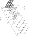
- FIG. 1 is an external perspective view of an image display apparatus according to an embodiment.
- FIG. 2 is an exploded perspective view of a liquid-crystal module according to the embodiment.
- FIG. 3 is a front view which illustrates a schematic configuration of a support pin according to the embodiment.
- FIG. 4 is a side view which illustrates a schematic configuration of the support pin according to the embodiment.
- FIG. 5 is a bottom view which illustrates a schematic configuration of the support pin according to the embodiment.
- FIG. 6 is an enlarged side view of a second portion according to the embodiment.
- FIG. 7 is a cross-sectional view which illustrates a base portion of a support according to the embodiment.
- FIG. 8 is a plan view which illustrates a schematic configuration of an opening portion of a back frame according to the embodiment.
- FIG. 9 is an explanatory diagram which illustrates a process of a procedure of assembling the support pin and the back frame according to the embodiment.
- FIG. 10 is an explanatory diagram which illustrates a process of the procedure of assembling the support pin and the back frame according to the embodiment.
- FIG. 11 is a side view of a pedestal of the support pin and the back frame according to the embodiment.
- FIG. 12 is a plan view which illustrates a schematic configuration of an opening portion of another back frame according to the embodiment.
- FIG. 13 is a bottom view which illustrates a process of a procedure of assembling the support pin and the other back frame according to the embodiment.
- FIG. 14 is a side view which illustrates the pedestal of the support pin and the other back frame according to the embodiment.
- FIG. 15 is an explanatory diagram which illustrates a positional relationship between the support pin and components disposed in proximity to the support pin, according to the embodiment.
- the Y-axis directions correspond to the up and down directions
- the Z-axis directions correspond to the back and front directions
- the X-axis directions correspond to the right and left directions, for convenience of description.
- such correspondences do not limit orientations of the image display apparatus according to present disclosure at the time of manufacturing or usage.
- an X-axis plus side refers to the direction of arrow of the X-axis
- an X-axis minus side refers to the side opposite to the X-axis plus side. The same holds true for the Y-axis direction and the Z-axis direction.
- FIG. 1 is an external perspective view of image display apparatus 10 according to the embodiment.
- FIG. 2 is an exploded perspective view of liquid-crystal module 100 according to the embodiment.
- image display apparatus 10 includes liquid-crystal module 100 , back cover 103 , stand 250 which supports liquid-crystal module 100 .
- Liquid-crystal module 100 is a device which displays a still image and video, and includes display panel 102 and bezel 120 provided along a peripheral edge of display panel 102 .
- display panel 102 is what is known as a liquid-crystal cell, and an element in which liquid crystal is contained between a plurality of glass plates.
- Display panel 102 is controlled according to an image signal input to liquid-crystal module 100 , and displays an image.
- Liquid-crystal module 100 including display panel 102 that is a liquid-crystal cell is referred to as, for example, a liquid-crystal module, etc., in some cases.
- bezel 120 is a component which has front portion 121 located on a front-surface side of display panel 102 , and is fixed to back frame 140 (see FIG. 2 ).
- bezel 120 is a component which protects periphery portions of elements such as display panel 102 , etc., and forms a frame by front portion 121 .
- resin such as polycarbonate (PC) or metal such as aluminum (Al), iron (Fe), etc. is employed as a material of bezel 120 .
- Bezel 120 and back frame 140 sandwich the components from display panel 102 to back frame 140 therebetween.
- Back cover 103 is a component that covers a rear surface of liquid-crystal module 100 , and includes resin such as PC or metal such as aluminum (Al), iron (Fe), etc., as with bezel 120 . It should be noted that back cover 103 may be a part of liquid-crystal module 100 .
- Liquid-crystal module 100 having the above-described configuration further includes: mold frame 130 ; optical sheet unit 105 including two or three optical sheets; diffuser plate 106 ; luminance uniforming plate 107 ; reflection sheet 108 ; LED sheet 109 ; relay sheet 110 ; back frame 140 ; and support pin 200 , as illustrated in FIG. 2 .
- Mold frame 130 supports display panel 102 . Mold frame 130 and back frame 140 sandwich a plurality of components from optical sheet unit 105 to LED sheet 109 and relay sheet 110 (what is known as a backlight).
- Optical sheet unit 105 has a configuration in which two or three types of sheets having different optical properties are stacked.
- Optical sheet unit 105 includes, for example, a vertical prism sheet, a crosswise prism sheet, a diffuser sheet, etc.
- Diffuser plate 106 diffuses light emitted from a plurality of LEDs 1091 (see FIG. 15 ) disposed on LED sheet 109 .
- Luminance uniforming plate 107 makes uniform luminance of the light which is emitted from the plurality of LEDs 1091 disposed on LED sheet 109 .
- Luminance uniforming plate 107 is also referred to as Flatter (registered trademark), for example.
- Luminance uniforming plate 107 is a component in which a plurality of openings 107 a having different diameters (see FIG. 15 ) are provided. More specifically, in luminance uniforming plate 107 , an opening with a significantly small diameter is formed directly above each of the plurality of LEDs 1091 . The diameter of openings increases with an increase in distance from LED 1091 .
- the above-described configuration allows luminance uniforming plate 107 to smooth distribution properties of light emitted from each of LEDs 1091 .
- Diffuser plate 106 further diffuses the light emitted from each of LEDs 1091 and having distribution properties smoothed by luminance uniforming plate 107 . Accordingly, diffuser plate 106 emits light with less luminance unevenness.
- Reflection sheet 108 is provided with openings 1081 (see FIG. 15 , etc.) at positions corresponding to the plurality of LEDs 1091 disposed on LED sheet 109 .
- LED sheet 109 is a flexible printed circuit board (FPC) on which the plurality of LEDs 1091 are disposed. Of two main surfaces of the FPC, one surface on which the plurality of LEDs 1091 are disposed is provided with a reflection layer. Of the two main surfaces of the FPC, the other surface is provided with a bonding layer.
- Relay sheet 110 is an FPC on which an electric path for supplying power, a control signal, etc., to the plurality of LEDs 1091 is formed. Relay sheet 110 is provided with a reflection layer, as with LED sheet 109 .
- Back frame 140 is made of a thin sheet metal, and supports LED sheet 109 and relay sheet 110 .
- Back frame 140 is also referred to as a base plate, in some cases. More specifically, after LED sheet 109 and relay sheet 110 are attached to back frame 140 , reflection sheet 108 is applied to back frame 140 such that LEDs 1091 are exposed respectively from the plurality of openings 1081 . Light emitted from each of LEDs 1091 is reflected by the reflection layer disposed above the FPC and reflection sheet 108 , and travels toward the Z-axis plus side.
- Support pins 200 are mounted from above reflection sheet 108 such that support pins 200 and back frame 140 hold reflection sheet 108 therebetween. Support pins 200 extend to penetrate through luminance uniforming plate 107 in a state in which support pins 200 are fixed to back frame 140 , and support diffuser plate 106 at tips thereof.
- Luminance uniforming plate 107 is provided with a plurality of openings into which support pins 200 are inserted, and support pins 200 are inserted into the respective openings.
- Diffuser plate 106 is supported by the tips of support pins 200 , and supported by back frame 140 at the peripheral edge portion of diffuser plate 106 .
- Back frame 140 has one side including a cut-and-raised portion for hanging optical sheet unit 105 .
- the one side of back frame 140 is an upper portion when image display apparatus 10 is installed.
- Optical sheet unit 105 includes a tab having a rectangular opening to be engaged with the above-described cut-and-raised portion.
- support pins 200 support diffuser plate 106 in such a manner that appearance of a dark portion is kept to a minimum.
- support pin 200 will be described in detail.
- FIG. 3 is a front view which illustrates a schematic configuration of support pin 200 according to the embodiment.
- FIG. 4 is a side view which illustrates a schematic configuration of support pin 200 according to the embodiment.
- FIG. 5 is a bottom view which illustrates a schematic configuration of support pin 200 according to the embodiment.
- support pin 200 is a resin component which includes pedestal 210 to be fixed to back frame 140 , and support 220 extending from pedestal 210 toward the front-surface side of display panel 102 .
- Pedestal 210 includes first portion 211 , second portion 212 , and connecting portion 213 .
- First portion 211 is a plate portion which has an elliptic shape in a plan view, and is in contact with first surface 142 of back frame 140 . More specifically, in the longitudinal direction of first portion 211 (X-axis direction according to the present embodiment), the center portion of first portion 211 is thin, and the end portions of first portion 211 are thick. As described above, since the center portion of first portion 211 is thin, first portion 211 is easily bent at the center portion. First portion 211 includes, at the end portions thereof, a pair of claws 214 which engage with opening portion 141 formed in back frame 140 . Each of the pair of claws 214 has a triangular shape in a front view as illustrated in FIG. 3 .
- each of the pair of claws 214 has a hexagonal shape in a bottom view as illustrated in FIG. 5 .
- Regions 215 which are the end portions, other than the pair of claws 214 , of first portion 211 are in contact with first surface 142 of back frame 140 .
- Second portion 212 is a plate portion which has an elliptic shape in a plan view, and is in contact with second surface 143 of back frame 140 . More specifically, the longitudinal direction of second portion 212 is a direction perpendicular to the longitudinal direction of first portion 211 (the Y-axis direction, according to the present embodiment). Second portion 212 is disposed within the center portion of first portion 211 in a plan view.
- FIG. 6 is an enlarged side view of second portion 212 according to the embodiment.
- second portion 212 has surface 216 which faces first portion 211 .
- Surface 216 is stepped. More specifically, surface 216 has a center portion that protrudes from end portions. The end portions of surface 216 is lower-step surface 217 , and the center portion of surface 216 is upper-step surface 218 .
- Space H 2 between lower-step surface 217 and region 215 of first portion 211 is greater than space H 1 between upper-step surface 218 and region 215 of first portion 211 .
- Back frame 140 and back frame 140 a are different in thickness, and each fitted in either space H 1 or space H 2 (see FIG. 11 and FIG. 14 ).
- first portion 211 and second portion 212 hold therebetween back frame 140 or back frame 140 a in a thickness direction of back frame 140 or back frame 140 a .
- first portion 211 and second portion 212 serve as a holding portion.
- Connecting portion 213 is a rectangular column which connects first portion 211 and second portion 212 . Connecting portion 213 extends from the center portion of first portion 211 to upper-step surface 218 of second portion 212 . Connecting portion 213 is disposed in opening portions 141 and 141 a of back frames 140 and 140 a , respectively (see FIG. 11 and FIG. 14 ).
- support 220 includes base portion 221 , middle portion 222 , and tip portion 223 .
- Base portion 221 is an end portion of support 220 which is adjacent to pedestal 210 .
- Base portion 221 is connected to the center portion of pedestal 210 .
- FIG. 7 is a cross-sectional view which illustrates base portion 221 of support 220 according to the embodiment. More specifically, FIG. 7 is a cross-sectional view taken along VII-VII indicated in FIG. 3 .
- base portion 221 is formed radially about axis S 1 of support 220 when viewed in the axis direction of support 220 . More specifically, base portion 221 is formed into a cross shape when viewed in the axis direction of support 220 .
- the two-dot chain line indicated in FIG. 7 is virtual circle C having a diameter substantially equivalent to width W of base portion 221 .
- the base portion of a support may have a cylindrical structure as indicated by virtual circle C, for example. However, with base portion 221 which is formed radially, it is possible to reduce materials while securing a certain level of strength.
- base portion 221 may have a shape other than the cross shape, as long as base portion 221 is formed radially about axis S 1 when viewed in the axis direction of support 220 .
- Other examples of the shape of base portion 221 include, for example, a multiangular star shape, a Y-shape, etc.
- Middle portion 222 is a portion between base portion 221 and tip portion 223 .
- Middle portion 222 includes, at an end portion adjacent to tip portion 223 , fitting portion 224 which has a cylindrical shape and is fitted in opening 107 a of luminance uniforming plate 107 .
- fitting portion 224 includes flange 225 at a position adjacent to middle portion 222 .
- Flange 225 has an outer diameter larger than an outer diameter of fitting portion 224 .
- Flange 225 prevents luminance uniforming plate 107 from moving toward base portion 221 .
- a portion between flange 225 and base portion 221 in middle portion 222 is thinner than base portion 221 .
- Tip portion 223 is a portion supporting diffuser plate 106 , and extends from middle portion 222 in the Z-axis direction. More specifically, a tip end of tip portion 223 has a shape of a convex curve, and the tip supports diffuser plate 106 .
- slit 229 which is parallel to a ZX plane is formed from the tip of tip portion 223 to a position halfway to middle portion 222 .
- back frames 140 and 140 a differ in thickness. More specifically, back frame 140 has a thickness corresponding to space H 2 , and back frame 140 a has a thickness corresponding to space H 1 . In other words, back frame 140 has a greater thickness than back frame 140 a.
- FIG. 8 is a plan view which illustrates a schematic configuration of opening portion 141 of back frame 140 according to the embodiment.
- Opening portion 141 is a through-hole elongated in the X-axis direction.
- Opening portion 141 includes first engagement opening 1411 , second engagement opening 1412 , and intermediate opening 1413 .
- First engagement opening 1411 and second engagement opening 1412 are end portions of opening portion 141 in the longitudinal direction.
- first engagement opening 1411 and second engagement opening 1412 are a pair of edge portions located at opposing positions in the longitudinal direction.
- Intermediate opening 1413 is a portion between first engagement opening 1411 and second engagement opening 1412 .
- First engagement opening 1411 is one end of opening portion 141 in the longitudinal direction. First engagement opening 1411 protrudes, in a rectangular shape, from one end of intermediate opening 1413 . One of the pair of claws 214 of support pin 200 engages with first engagement opening 1411 .
- Second engagement opening 1412 is the other end of opening portion 141 in the longitudinal direction. Second engagement opening 1412 protrudes, in a rectangular shape, from the other end of intermediate opening 1413 . Second engagement opening 1412 protrudes to have a longer protrusion length than a protrusion length of first engagement opening 1411 . The other of the pair of claws 214 of support pin 200 is guided into second engagement opening 1412 and engages with second engagement opening 1412 .
- second engagement opening 1412 has a width same as width W 1 of upper-step surface 218 of second portion 212 , and upper-step surface 218 is fitted in second engagement opening 1412 (see FIG. 11 ).
- Intermediate opening 1413 has a size that allows second portion 212 of support pin 200 to penetrate through in a non-contact manner.
- the other end of intermediate opening 1413 has an oblique shape in a plan view such that the width of intermediate opening 1413 gradually decreases toward second engagement opening 1412 .
- the other end of intermediate opening 1413 serves as a guide portion for guiding upper-step surface 218 of second portion 212 into the second engagement opening 1412 at the time of attaching support pin 200 into opening portion 141 .
- FIG. 9 and FIG. 10 are explanatory diagrams which illustrate a process of the procedure of assembling support pin 200 to back frame 140 according to the embodiment.
- FIG. 11 is a side view of pedestal 210 of support pin 200 and back frame 140 according to the embodiment. It should be noted that only back frame 140 is illustrated in a cross-sectional view in FIG. 11 .
- an operator inserts the other of the pair of claws 214 of support pin 200 into second engagement opening 1412 of opening portion 141 , and inserts second portion 212 into intermediate opening 1413 . At this time, the operator bends the center portion of first portion 211 of support pin 200 , thereby facilitating the above-described inserting operation.
- the operator slides the other of the pair of claws 214 along second engagement opening 1412 , and thereby moves the other of the pair of claws 214 to a tip end potion of second engagement opening 1412 .
- the one of the pair of claws 214 also enters and engages with first engagement opening 1411 .
- FIG. 12 is a plan view which illustrates a schematic configuration of opening portion 141 a of back frame 140 a according to the embodiment. Opening portion 141 a is different from opening portion 141 in that enlarged-width area 1414 a is included in second engagement opening 1412 a . Accordingly, in the description below, the same portions as opening portion 141 are assigned with the same reference signs, and the description for the same portions will be omitted.
- Second engagement opening 1412 a includes, at an end portion adjacent to intermediate opening 1413 , enlarged-width area 1414 a which has a width greater than the other portion of second engagement opening 1412 a .
- the width of enlarged-width area 1414 a is the same as width W 2 of connecting portion 213 such that connecting portion 213 is fitted in enlarged-width area 1414 a (see FIG. 14 ).
- support pin 200 is also attached to back frame 140 a according to a procedure same as or similar to the above-described procedure applied to back frame 140 .
- FIG. 13 is a bottom view of pedestal 210 which illustrates a state after back frame 140 a and support pin 200 are assembled together, according to the embodiment.
- FIG. 14 is a side view of pedestal 210 of support pin 200 and back frame 140 a according to the embodiment. It should be noted that only back frame 140 a is illustrated in a cross-sectional view in FIG. 14 .
- connecting portion 213 is fitted in enlarged-width area 1414 a .
- back frame 140 a is fitted in space H 1 . More specifically, region 215 of first portion 211 is in contact with first surface 142 a of back frame 140 a , and upper-step surface 218 of second portion 212 is in contact with second surface 143 a of back frame 140 a . Accordingly, the holding portion (first portion 211 and second portion 212 ) holds back frame 140 a between first portion 211 and second portion 212 , in a sandwiching manner, in the thickness direction.
- the longitudinal direction of opening portions 141 and 141 a is the X-axis direction
- the longitudinal direction of opening portions 141 and 141 a may be arbitrarily arranged in the XY plane.
- the following describes a positional relationship between support pin 200 and components disposed in proximity to support pin 200 , after assembling, according to the embodiment.
- FIG. 15 is an explanatory diagram which illustrates a positional relationship between support pin 200 and components disposed in proximity to support pin 200 , according to the embodiment.
- reflection sheet 108 is disposed on a front-surface side of back frame 140 .
- a plurality of openings 1081 for individually exposing a plurality of LEDs 1091 of LED sheet 109 (illustration omitted) are provided in reflection sheet 108 .
- Luminance uniforming plate 107 is disposed on a front-surface side of reflection sheet 108 with a predetermined space therebetween.
- Diffuser plate 106 is disposed on a front-surface side of luminance uniforming plate 107 with a predetermined space therebetween.
- Support pin 200 includes support 220 which extends to penetrate through luminance uniforming plate 107 in a state in which support pin 200 is fixed to back frame 140 .
- Support 220 includes fitting portion 224 which is fitted in opening 107 a of luminance uniforming plate 107 .
- a tip end of tip portion 223 of support 220 has a shape of a convex curve, and thus is in point contact with diffuser plate 106 . In this manner, since the tip end of support pin 200 is in point contact with diffuser plate 106 , light L emitted by LED 1091 is less likely to be blocked, and thus it is possible to inhibit production of a dark portion.
- image display apparatus 10 includes: back frame 140 or 140 a disposed on a rear-surface side of display panel 102 ; a plurality of light-emitting diodes (LEDs) 1091 disposed on a front-surface side of back frame 140 or 140 a ; luminance uniforming plate 107 which is disposed on a front-surface side of the plurality of LEDs 1091 to cover the plurality of LEDs 1091 , and makes uniform luminance of light emitted by the plurality of LEDs 1091 ; diffuser plate 106 which is disposed on a front-surface side of luminance uniforming plate 107 , and diffuses light transmitted through luminance uniforming plate 107 ; and support pin 200 which is fixed to back frame 140 or 140 a , extends to penetrate through luminance uniforming plate 107 , and has a tip end that supports diffuser plate 106 .
- LEDs light-emitting diodes
- support pin 200 includes: pedestal 210 which is fixed to opening portion 141 or 141 a formed in back frame 140 or 140 a ; and support 220 which includes the tip end, and extends from pedestal 210 toward a front-surface side of display panel 102 .
- Pedestal 210 includes holding portion (first portion 211 and second portion 212 ) which holds, in a sandwiching manner, back frame 140 or 140 a in a thickness direction of back frame 140 or 140 a , and a portion of the holding portion on which back frame 140 or 140 a is disposed is stepped.
- support pin 200 is support pin 200 included in liquid-crystal module 100 that includes: back frame 140 or 140 a disposed on a rear-surface side of display panel 102 ; a plurality of light-emitting diodes (LEDs) 1091 disposed on a front-surface side of back frame 140 or 140 a ; luminance uniforming plate 107 which is disposed on a front-surface side of the plurality of LEDs 1091 to cover the plurality of LEDs 1091 , and makes uniform luminance of light emitted by the plurality of LEDs 1091 ; and diffuser plate 106 which is disposed on a front-surface side of luminance uniforming plate 107 , and diffuses light transmitted through luminance uniforming plate 107 .
- LEDs light-emitting diodes
- Support pin 200 includes: pedestal 210 which is fixed to opening portion 141 or 141 a formed in back frame 140 or 140 a ; and support 220 which extends from pedestal 2101 toward a front-surface side of display panel 102 to penetrate through luminance uniforming plate 107 , and has a tip end that supports diffuser plate 106 .
- Pedestal 210 includes a holding portion which holds, in a sandwiching manner, back frame 140 or 140 a in a thickness direction of back frame 140 or 140 a , and the holding portion is stepped.
- the holding portion includes: first portion 211 which is in contact with first surface 142 or 142 a of back frame 140 or 140 a ; and second portion 212 which faces first portion 211 , and is in contact with second surface 143 or 143 a of back frame 140 or 140 a , and at least one of first portion 211 and second portion 212 is stepped.
- first portion 211 and second portion 212 are stepped, it is possible to form spaces H 1 and H 2 which are different in size with a simple configuration.
- pedestal 210 includes a pair of claws 214 which engage with a pair of edge portions (first engagement opening 1411 and second engagement opening 1412 , 1412 a ) located at opposing positions in opening portion 141 or 141 a of back frame 140 or 140 a.
- tip end of support pin 200 has a shape of a convex curve.
- the tip end of support pin 200 which supports diffuser plate 106 has a shape of a convex curve, and thus the tip end of support pin 200 is in point contact with diffuser plate 106 . It is thus possible to reduce the amount of light L blocked by support pin 200 , making it possible to inhibit luminance unevenness.
- support 220 does not have to be thinned as a whole, it is also possible to maintain the strength of support 220 . As a result, it is possible to inhibit luminance unevenness caused by support pin 200 while maintaining the strength of support pin 200 .
- a plurality of support pins 200 support luminance uniforming plate 107 in a state in which the plurality of support pins 200 penetrate through luminance uniforming plate 107 .
- accumulation of dimensional tolerances or installation errors due to individual variability among support pins 200 causes slight misalignment in positional relationships between the plurality of openings 107 a of luminance uniforming plate 107 and the plurality of support pins 200 .
- some support pins 200 may be tilted in some cases.
- the tip end of support pin 200 has a shape of a convex curve, and thus the tip end of support pin 200 is in point contact with diffuser plate 106 . It is thus possible to inhibit luminance unevenness even when support pin 200 is tilted. Moreover, as described above, since the strength of support pin 200 is maintained, support pin 200 is less susceptible to damage even when external force in a direction in which support pin 200 is tilted is applied to support pin 200 .
- support pin 200 includes: pedestal 210 to be fixed to back frame 140 or 140 a ; and support 220 which includes the tip end, and extends from pedestal 210 toward a front-surface side of display panel 102 .
- Support pin 200 includes, between pedestal 210 and a part (fitting portion 224 ) at which support 220 is fitted in luminance uniforming plate 107 , a portion (portion between flange 225 and base portion 221 ) formed thinner than remaining portions (base portion 221 ) between pedestal 210 and the part.
- support 220 since support 220 includes a portion formed thinner between fitting portion 224 and pedestal 210 than the remaining portion between fitting portion 224 and pedestal 210 , support pin 200 is easily elastically deformed at the portion formed thinner. As described above, when external force in a direction in which support pin 200 is tilted is applied to support pin 200 , the portion formed thinner is elastically deformed. In other words, the external force applied by luminance uniforming plate 107 is easily absorbed by support pin 200 , and this it is possible to maintain planarity of luminance uniforming plate 107 .
- support 220 has an end portion (base portion 221 ) adjacent to pedestal 210 , the end portion being formed radially about an axis of support 220 when viewed in an axis direction of support 220 .
- base portion 221 is formed radially, it is possible to reduce materials while securing the strength of base portion 221 .
- the tip end of support 220 is split, and when support 220 penetrates through luminance uniforming plate 107 , the tip end is restrained by luminance uniforming plate 107 and is thinner in comparison to a state before the tip end is restrained.
- support 220 having a split tip end is thinner in comparison to the state before support 220 is restrained. It is thus possible to smoothly attach support pin 200 to luminance uniforming plate 107 .
- an edge-lit backlight unit which emits light that is incident on an end surface of a light guide toward display panel 102 from a front surface of the light guide may be included in liquid-crystal module 100 .
- image display apparatus 10 includes liquid-crystal module 100 as an apparatus which displays a still image and video.
- liquid-crystal module 100 may be applied to, for example, a monitor display or the like for use in a personal computer.
- resin such as PC is employed for mold frame 130 .
- metal such as steel use stainless (SUS) may be employed as a material for mold frame 130 .
- SUS steel use stainless
- metal is employed for four sides (linear portions) of mold frame 130 , four corners may be formed using resin rather than metal.
- second portion 212 of support pin 200 is stepped has been described as an example.
- each of the first portion and the second portion may be stepped.
- stepped shape of support pin 200 may be defined by three or more steps. With this, since three or more spaces which are different in size are formed, it is possible to implement a support pin which can be applied to larger number of types of back frames.
- support 220 includes a portion (i.e., a portion between flange 225 and base portion 221 ) formed thinner between fitting portion 224 and pedestal 210 than the remaining portion (base portion 221 ) between fitting portion 224 and pedestal 210 has been described as an example.
- the portion i.e., a portion between flange 225 and base portion 221
- base portion 221 is formed radially has been described as an example.
- base portion 221 need not be formed radially.
- Other examples of the shape of the base portion include, for example, a polygonal shape, a circular shape, etc.
- support 220 has a split end
- support 220 may have a shape without a split end.
- the structural components described in the accompanying Drawings and the detailed description may include not only the structural components which are essential for solving the problems but also the structural components which are not essential for solving the problems but used for exemplifying the above-described techniques.
- description of these non-essential structural components in the accompanying drawings and the detailed description should not be taken to mean that these non-essential structural components are essential.
- the present disclosure is applicable to an image display apparatus which includes, for example, a support pin. More specifically, the present disclosure is applicable to a television receiver, a monitor display, a digital signage, a table-type display apparatus, etc.
Landscapes
- Physics & Mathematics (AREA)
- Nonlinear Science (AREA)
- General Physics & Mathematics (AREA)
- Optics & Photonics (AREA)
- Crystallography & Structural Chemistry (AREA)
- Chemical & Material Sciences (AREA)
- Mathematical Physics (AREA)
- Engineering & Computer Science (AREA)
- Liquid Crystal (AREA)
- Theoretical Computer Science (AREA)
- Multimedia (AREA)
- Signal Processing (AREA)
- Devices For Indicating Variable Information By Combining Individual Elements (AREA)
- Planar Illumination Modules (AREA)
Abstract
Description
Claims (3)
Priority Applications (1)
| Application Number | Priority Date | Filing Date | Title |
|---|---|---|---|
| US16/091,950 US10914984B2 (en) | 2017-02-09 | 2018-02-06 | Image display apparatus and support pin |
Applications Claiming Priority (5)
| Application Number | Priority Date | Filing Date | Title |
|---|---|---|---|
| US201762456939P | 2017-02-09 | 2017-02-09 | |
| JP2017-161534 | 2017-08-24 | ||
| JP2017161534 | 2017-08-24 | ||
| US16/091,950 US10914984B2 (en) | 2017-02-09 | 2018-02-06 | Image display apparatus and support pin |
| PCT/JP2018/004003 WO2018147272A1 (en) | 2017-02-09 | 2018-02-06 | Image display device and support pin |
Publications (2)
| Publication Number | Publication Date |
|---|---|
| US20190137827A1 US20190137827A1 (en) | 2019-05-09 |
| US10914984B2 true US10914984B2 (en) | 2021-02-09 |
Family
ID=66327191
Family Applications (1)
| Application Number | Title | Priority Date | Filing Date |
|---|---|---|---|
| US16/091,950 Expired - Fee Related US10914984B2 (en) | 2017-02-09 | 2018-02-06 | Image display apparatus and support pin |
Country Status (3)
| Country | Link |
|---|---|
| US (1) | US10914984B2 (en) |
| EP (1) | EP3582207B1 (en) |
| JP (1) | JP6945148B2 (en) |
Cited By (1)
| Publication number | Priority date | Publication date | Assignee | Title |
|---|---|---|---|---|
| US20220317504A1 (en) * | 2016-07-15 | 2022-10-06 | Saturn Licensing Llc | Display device |
Families Citing this family (1)
| Publication number | Priority date | Publication date | Assignee | Title |
|---|---|---|---|---|
| CN114415424B (en) * | 2017-11-20 | 2025-02-28 | 群创光电股份有限公司 | Backlight module and display device |
Citations (37)
| Publication number | Priority date | Publication date | Assignee | Title |
|---|---|---|---|---|
| US2271012A (en) | 1939-08-07 | 1942-01-27 | Cleveland Pneumatic Tool Co | Riveting clamp |
| JP2005316337A (en) | 2004-04-30 | 2005-11-10 | Sony Corp | Backlight device |
| US20050281050A1 (en) | 2004-06-18 | 2005-12-22 | Au Optronics Corp. | Support member and light emitting diode module using the same |
| US20060104080A1 (en) | 2004-11-17 | 2006-05-18 | Kim Won-Nyun | Backlight unit and LCD display apparatus having the same |
| US20060215386A1 (en) * | 2003-09-19 | 2006-09-28 | Masato Hatanaka | Backlight device and liquid crystal display |
| US20070070651A1 (en) | 2004-11-30 | 2007-03-29 | Sharp Kabushiki Kaisha | Lamp holding apparatus, lighting device for display device including same, display device including same and liquid crystal display device including lighting device for display device |
| JP2007157451A (en) | 2005-12-02 | 2007-06-21 | Sharp Corp | Diffusion plate support member, backlight device, and display device |
| US20080106905A1 (en) * | 2006-11-02 | 2008-05-08 | Au Optronics Corp. | Supporting structure and backlight module using the same |
| US20080159835A1 (en) | 2006-12-29 | 2008-07-03 | Lg Philips Lcd Co., Ltd. | Glass support pin |
| US20080225556A1 (en) * | 2007-03-12 | 2008-09-18 | Po-Chun Chen | Fastening apparatus for a backlight assembly |
| US20080285268A1 (en) | 2004-11-09 | 2008-11-20 | Takashi Oku | Backlight Device |
| US20090154139A1 (en) * | 2007-12-18 | 2009-06-18 | Kyung Ho Shin | Light emitting module connecting apparatus, light unit having the same, and display device |
| JP2009211843A (en) | 2008-02-29 | 2009-09-17 | Sharp Corp | Lighting system, display device, and television |
| US20100008066A1 (en) * | 2008-06-18 | 2010-01-14 | Sony Corporation | Clip and backlight assembly |
| WO2010052957A1 (en) | 2008-11-05 | 2010-05-14 | シャープ株式会社 | Support unit, lighting device, and display device |
| US20100284172A1 (en) * | 2008-03-06 | 2010-11-11 | Sharp Kabushiki Kaisha | Lighting device and display device |
| WO2011010488A1 (en) | 2009-07-21 | 2011-01-27 | シャープ株式会社 | Lens unit, light emitting module, illumination device, display device, and television receiving device |
| WO2011016271A1 (en) | 2009-08-07 | 2011-02-10 | シャープ株式会社 | Illumination device, display device, and television receiving device |
| US20110242435A1 (en) * | 2008-12-18 | 2011-10-06 | Sharp Kabushiki Kaisha | Illumination device, display device, and television receiver |
| US20110317095A1 (en) * | 2009-03-04 | 2011-12-29 | Sharp Kabushiki Kaisha | Supporting unit, sheet set, illuminating device, and display device |
| US20120081634A1 (en) * | 2009-06-15 | 2012-04-05 | Sharp Kabushiki Kaisha | Lighting device, display device and television receiver |
| US20120120325A1 (en) * | 2009-07-21 | 2012-05-17 | Sharp Kabushiki Kaisha | Support pin, illumination device, display device, and television receiving device |
| US8218107B2 (en) | 2008-04-28 | 2012-07-10 | Lg Display Co., Ltd. | Backlight unit and liquid crystal display device including the same |
| US20130188100A1 (en) * | 2009-12-02 | 2013-07-25 | Sharp Kabushiki Kaisha | Lighting device, display device and television receiver |
| US20130194529A1 (en) | 2012-01-30 | 2013-08-01 | Chimei Innolux Corporation | Backlight module and display device including the same |
| US20130201663A1 (en) * | 2012-02-07 | 2013-08-08 | Samsung Electronic Co., Ltd. | Supporting member for backlight unit, backlight unit and image display apparatus having the same |
| US20130215356A1 (en) * | 2012-02-16 | 2013-08-22 | Yajun Yu | Connecting Piece for Backlight Module, Backlight Module and LCD Device |
| US20140022763A1 (en) | 2012-07-19 | 2014-01-23 | Sony Corporation | Display device |
| US20140086704A1 (en) * | 2011-06-02 | 2014-03-27 | A. Raymond Et Cie | Fasteners manufactured by three-dimensional printing |
| EP2840440A1 (en) | 2013-08-20 | 2015-02-25 | Funai Electric Co., Ltd. | Display device |
| US20150261042A1 (en) | 2014-03-17 | 2015-09-17 | Nlt Technologies, Ltd. | Surface light-emitting device and liquid crystal display apparatus |
| US20160114738A1 (en) * | 2014-10-28 | 2016-04-28 | Ford Global Technologies, Llc | Clip for fastening coverings to a vehicle body |
| US20160223726A1 (en) * | 2015-02-02 | 2016-08-04 | Samsung Display Co., Ltd. | Optical member supporter and curved display device including the same |
| US20160377951A1 (en) * | 2015-06-29 | 2016-12-29 | E Ink Corporation | Method for mechnical and electrical connection to display electrodes |
| WO2017002308A1 (en) | 2015-07-01 | 2017-01-05 | パナソニックIpマネジメント株式会社 | Backlight device and liquid crystal display device |
| WO2017002307A1 (en) | 2015-07-01 | 2017-01-05 | パナソニックIpマネジメント株式会社 | Backlight device and liquid-crystal display device |
| US20180004034A1 (en) * | 2016-07-04 | 2018-01-04 | Lg Electronics Inc. | Display device |
Family Cites Families (1)
| Publication number | Priority date | Publication date | Assignee | Title |
|---|---|---|---|---|
| JP5351723B2 (en) * | 2009-05-22 | 2013-11-27 | シャープ株式会社 | Light source device and display device |
-
2018
- 2018-02-06 US US16/091,950 patent/US10914984B2/en not_active Expired - Fee Related
- 2018-02-06 EP EP18751613.3A patent/EP3582207B1/en not_active Not-in-force
- 2018-02-06 JP JP2018533957A patent/JP6945148B2/en not_active Expired - Fee Related
Patent Citations (45)
| Publication number | Priority date | Publication date | Assignee | Title |
|---|---|---|---|---|
| US2271012A (en) | 1939-08-07 | 1942-01-27 | Cleveland Pneumatic Tool Co | Riveting clamp |
| US20060215386A1 (en) * | 2003-09-19 | 2006-09-28 | Masato Hatanaka | Backlight device and liquid crystal display |
| JP2005316337A (en) | 2004-04-30 | 2005-11-10 | Sony Corp | Backlight device |
| US20050281050A1 (en) | 2004-06-18 | 2005-12-22 | Au Optronics Corp. | Support member and light emitting diode module using the same |
| US20080285268A1 (en) | 2004-11-09 | 2008-11-20 | Takashi Oku | Backlight Device |
| US20060104080A1 (en) | 2004-11-17 | 2006-05-18 | Kim Won-Nyun | Backlight unit and LCD display apparatus having the same |
| US20070070651A1 (en) | 2004-11-30 | 2007-03-29 | Sharp Kabushiki Kaisha | Lamp holding apparatus, lighting device for display device including same, display device including same and liquid crystal display device including lighting device for display device |
| JP2007157451A (en) | 2005-12-02 | 2007-06-21 | Sharp Corp | Diffusion plate support member, backlight device, and display device |
| US20080106905A1 (en) * | 2006-11-02 | 2008-05-08 | Au Optronics Corp. | Supporting structure and backlight module using the same |
| US20080159835A1 (en) | 2006-12-29 | 2008-07-03 | Lg Philips Lcd Co., Ltd. | Glass support pin |
| US20080225556A1 (en) * | 2007-03-12 | 2008-09-18 | Po-Chun Chen | Fastening apparatus for a backlight assembly |
| US20090154139A1 (en) * | 2007-12-18 | 2009-06-18 | Kyung Ho Shin | Light emitting module connecting apparatus, light unit having the same, and display device |
| JP2009211843A (en) | 2008-02-29 | 2009-09-17 | Sharp Corp | Lighting system, display device, and television |
| US20100284172A1 (en) * | 2008-03-06 | 2010-11-11 | Sharp Kabushiki Kaisha | Lighting device and display device |
| US8218107B2 (en) | 2008-04-28 | 2012-07-10 | Lg Display Co., Ltd. | Backlight unit and liquid crystal display device including the same |
| US20100008066A1 (en) * | 2008-06-18 | 2010-01-14 | Sony Corporation | Clip and backlight assembly |
| WO2010052957A1 (en) | 2008-11-05 | 2010-05-14 | シャープ株式会社 | Support unit, lighting device, and display device |
| US20110199754A1 (en) | 2008-11-05 | 2011-08-18 | Sharp Kabushiki Kaisha | Support unit, lighting device, and display device |
| US20110242435A1 (en) * | 2008-12-18 | 2011-10-06 | Sharp Kabushiki Kaisha | Illumination device, display device, and television receiver |
| US20110317095A1 (en) * | 2009-03-04 | 2011-12-29 | Sharp Kabushiki Kaisha | Supporting unit, sheet set, illuminating device, and display device |
| US20120081634A1 (en) * | 2009-06-15 | 2012-04-05 | Sharp Kabushiki Kaisha | Lighting device, display device and television receiver |
| US20120105739A1 (en) | 2009-07-21 | 2012-05-03 | Sharp Kabushiki Kaisha | Lens unit, light emitting-module, illumination device, display device and television receiver |
| US20120120325A1 (en) * | 2009-07-21 | 2012-05-17 | Sharp Kabushiki Kaisha | Support pin, illumination device, display device, and television receiving device |
| WO2011010488A1 (en) | 2009-07-21 | 2011-01-27 | シャープ株式会社 | Lens unit, light emitting module, illumination device, display device, and television receiving device |
| WO2011016271A1 (en) | 2009-08-07 | 2011-02-10 | シャープ株式会社 | Illumination device, display device, and television receiving device |
| US20120133845A1 (en) | 2009-08-07 | 2012-05-31 | Sharp Kabushiki Kaisha | Illumination device, display device, and television receiving device |
| US20130188100A1 (en) * | 2009-12-02 | 2013-07-25 | Sharp Kabushiki Kaisha | Lighting device, display device and television receiver |
| US20140086704A1 (en) * | 2011-06-02 | 2014-03-27 | A. Raymond Et Cie | Fasteners manufactured by three-dimensional printing |
| US20130194529A1 (en) | 2012-01-30 | 2013-08-01 | Chimei Innolux Corporation | Backlight module and display device including the same |
| US20130201663A1 (en) * | 2012-02-07 | 2013-08-08 | Samsung Electronic Co., Ltd. | Supporting member for backlight unit, backlight unit and image display apparatus having the same |
| JP2013161793A (en) | 2012-02-07 | 2013-08-19 | Samsung Electronics Co Ltd | Support member for backlight unit, backlight unit having the same, and image display device |
| US20130215356A1 (en) * | 2012-02-16 | 2013-08-22 | Yajun Yu | Connecting Piece for Backlight Module, Backlight Module and LCD Device |
| JP2014022208A (en) | 2012-07-19 | 2014-02-03 | Sony Corp | Display device |
| US20140022763A1 (en) | 2012-07-19 | 2014-01-23 | Sony Corporation | Display device |
| EP2840440A1 (en) | 2013-08-20 | 2015-02-25 | Funai Electric Co., Ltd. | Display device |
| US20150261042A1 (en) | 2014-03-17 | 2015-09-17 | Nlt Technologies, Ltd. | Surface light-emitting device and liquid crystal display apparatus |
| JP2015176780A (en) | 2014-03-17 | 2015-10-05 | Nltテクノロジー株式会社 | Surface light-emitting device and liquid crystal display device |
| US20160114738A1 (en) * | 2014-10-28 | 2016-04-28 | Ford Global Technologies, Llc | Clip for fastening coverings to a vehicle body |
| US20160223726A1 (en) * | 2015-02-02 | 2016-08-04 | Samsung Display Co., Ltd. | Optical member supporter and curved display device including the same |
| US20160377951A1 (en) * | 2015-06-29 | 2016-12-29 | E Ink Corporation | Method for mechnical and electrical connection to display electrodes |
| WO2017002308A1 (en) | 2015-07-01 | 2017-01-05 | パナソニックIpマネジメント株式会社 | Backlight device and liquid crystal display device |
| WO2017002307A1 (en) | 2015-07-01 | 2017-01-05 | パナソニックIpマネジメント株式会社 | Backlight device and liquid-crystal display device |
| US20180107068A1 (en) | 2015-07-01 | 2018-04-19 | Panasonic Intellectual Property Management Co., Ltd. | Backlight device and liquid crystal display device |
| US20180107067A1 (en) | 2015-07-01 | 2018-04-19 | Panasonic Intellectual Property Management Co., Ltd. | Backlight device and liquid-crystal display device |
| US20180004034A1 (en) * | 2016-07-04 | 2018-01-04 | Lg Electronics Inc. | Display device |
Non-Patent Citations (7)
| Title |
|---|
| European Office Action issued in European Patent Application No. 18 751 074.8, dated Sep. 9, 2020. |
| Extemded European Search Report issued in corresponding European Patent Application No. 18751074.8, dated Nov. 21, 2019. |
| Extemded European Search Report issued in corresponding European Patent Application No. 18751613.3, dated Nov. 21, 2019. |
| International Search Report issued in International Application No. PCT/JP2018/004002 dated Apr. 24, 2018. |
| International Search Report issued in International Application No. PCT/JP2018/004003 dated Apr. 24, 2018. |
| Non-Final Office Action issued in U.S. Appl. No. 16/091,924, dated Aug. 19, 2020. |
| Non-Final Office Action issued in U.S. Appl. No. 16/091,924, dated Jul. 26, 2019. |
Cited By (3)
| Publication number | Priority date | Publication date | Assignee | Title |
|---|---|---|---|---|
| US20220317504A1 (en) * | 2016-07-15 | 2022-10-06 | Saturn Licensing Llc | Display device |
| US12007635B2 (en) * | 2016-07-15 | 2024-06-11 | Saturn Licensing Llc | Display device |
| US12393068B2 (en) | 2016-07-15 | 2025-08-19 | Saturn Licensing Llc | Display device |
Also Published As
| Publication number | Publication date |
|---|---|
| US20190137827A1 (en) | 2019-05-09 |
| EP3582207A1 (en) | 2019-12-18 |
| JPWO2018147272A1 (en) | 2019-11-21 |
| EP3582207A4 (en) | 2019-12-25 |
| JP6945148B2 (en) | 2021-10-06 |
| EP3582207B1 (en) | 2021-12-22 |
Similar Documents
| Publication | Publication Date | Title |
|---|---|---|
| KR101312212B1 (en) | Lighting device, display apparatus, and television receiving equipment | |
| US9207476B2 (en) | Liquid crystal display device and method of fabricating the same | |
| US9477124B2 (en) | Display device and television device | |
| JP5616988B2 (en) | Support member for backlight unit, backlight unit and video display device including the same | |
| US9823509B2 (en) | Display device | |
| US8045091B2 (en) | Backlight unit and dislay device having the same | |
| US9541779B2 (en) | Display device including a curvature maintaining bar | |
| US10564453B2 (en) | Display device | |
| US20120086885A1 (en) | Lighting device, display device and television receiver | |
| US20180231839A1 (en) | Lighting device, display device, and television device | |
| US9658390B2 (en) | Light source cover including groove and backlight assembly including the light source cover | |
| US10914985B2 (en) | Image display apparatus and support pin | |
| US20180157115A1 (en) | Edge-lit backlight device and liquid crystal display device | |
| US10914984B2 (en) | Image display apparatus and support pin | |
| JP2014022208A (en) | Display device | |
| US20160131828A1 (en) | Illumination device, display device, and tv receiver | |
| US8958029B2 (en) | Liquid crystal display device | |
| CN101960213B (en) | Illuminating apparatus, display apparatus and television receiving apparatus | |
| US20150146111A1 (en) | Display device and television device | |
| US20200257031A1 (en) | Display device | |
| WO2018147272A1 (en) | Image display device and support pin | |
| EP4372267A1 (en) | Planar lighting device | |
| TWI408462B (en) | Backlight module and liquid crystal display | |
| WO2018147271A1 (en) | Image display device and support pin | |
| US9207391B2 (en) | Backlight module and liquid crystal display |
Legal Events
| Date | Code | Title | Description |
|---|---|---|---|
| FEPP | Fee payment procedure |
Free format text: ENTITY STATUS SET TO UNDISCOUNTED (ORIGINAL EVENT CODE: BIG.); ENTITY STATUS OF PATENT OWNER: LARGE ENTITY |
|
| AS | Assignment |
Owner name: PANASONIC INTELLECTUAL PROPERTY MANAGEMENT CO., LT Free format text: ASSIGNMENT OF ASSIGNORS INTEREST;ASSIGNORS:KUGIMARU, TADAHIRO;TAKEUCHI, TAIZOU;UMITANI, TAKAFUMI;REEL/FRAME:048537/0044 Effective date: 20180920 Owner name: PANASONIC INTELLECTUAL PROPERTY MANAGEMENT CO., LTD., JAPAN Free format text: ASSIGNMENT OF ASSIGNORS INTEREST;ASSIGNORS:KUGIMARU, TADAHIRO;TAKEUCHI, TAIZOU;UMITANI, TAKAFUMI;REEL/FRAME:048537/0044 Effective date: 20180920 |
|
| STPP | Information on status: patent application and granting procedure in general |
Free format text: NON FINAL ACTION MAILED |
|
| STPP | Information on status: patent application and granting procedure in general |
Free format text: RESPONSE TO NON-FINAL OFFICE ACTION ENTERED AND FORWARDED TO EXAMINER |
|
| STPP | Information on status: patent application and granting procedure in general |
Free format text: ADVISORY ACTION MAILED |
|
| STPP | Information on status: patent application and granting procedure in general |
Free format text: DOCKETED NEW CASE - READY FOR EXAMINATION |
|
| STPP | Information on status: patent application and granting procedure in general |
Free format text: NON FINAL ACTION MAILED |
|
| STPP | Information on status: patent application and granting procedure in general |
Free format text: NOTICE OF ALLOWANCE MAILED -- APPLICATION RECEIVED IN OFFICE OF PUBLICATIONS |
|
| STCF | Information on status: patent grant |
Free format text: PATENTED CASE |
|
| FEPP | Fee payment procedure |
Free format text: MAINTENANCE FEE REMINDER MAILED (ORIGINAL EVENT CODE: REM.); ENTITY STATUS OF PATENT OWNER: LARGE ENTITY |
|
| LAPS | Lapse for failure to pay maintenance fees |
Free format text: PATENT EXPIRED FOR FAILURE TO PAY MAINTENANCE FEES (ORIGINAL EVENT CODE: EXP.); ENTITY STATUS OF PATENT OWNER: LARGE ENTITY |
|
| STCH | Information on status: patent discontinuation |
Free format text: PATENT EXPIRED DUE TO NONPAYMENT OF MAINTENANCE FEES UNDER 37 CFR 1.362 |
|
| FP | Lapsed due to failure to pay maintenance fee |
Effective date: 20250209 |