US10897241B2 - Hysteresis control method for inverter and an inverter with hysteresis control - Google Patents
Hysteresis control method for inverter and an inverter with hysteresis control Download PDFInfo
- Publication number
- US10897241B2 US10897241B2 US16/718,104 US201916718104A US10897241B2 US 10897241 B2 US10897241 B2 US 10897241B2 US 201916718104 A US201916718104 A US 201916718104A US 10897241 B2 US10897241 B2 US 10897241B2
- Authority
- US
- United States
- Prior art keywords
- hysteresis
- bandwidth
- inverter
- next period
- bus
- Prior art date
- Legal status (The legal status is an assumption and is not a legal conclusion. Google has not performed a legal analysis and makes no representation as to the accuracy of the status listed.)
- Active
Links
Images

Classifications
-
- H—ELECTRICITY
- H02—GENERATION; CONVERSION OR DISTRIBUTION OF ELECTRIC POWER
- H02M—APPARATUS FOR CONVERSION BETWEEN AC AND AC, BETWEEN AC AND DC, OR BETWEEN DC AND DC, AND FOR USE WITH MAINS OR SIMILAR POWER SUPPLY SYSTEMS; CONVERSION OF DC OR AC INPUT POWER INTO SURGE OUTPUT POWER; CONTROL OR REGULATION THEREOF
- H02M7/00—Conversion of AC power input into DC power output; Conversion of DC power input into AC power output
- H02M7/42—Conversion of DC power input into AC power output without possibility of reversal
- H02M7/44—Conversion of DC power input into AC power output without possibility of reversal by static converters
- H02M7/48—Conversion of DC power input into AC power output without possibility of reversal by static converters using discharge tubes with control electrode or semiconductor devices with control electrode
- H02M7/53—Conversion of DC power input into AC power output without possibility of reversal by static converters using discharge tubes with control electrode or semiconductor devices with control electrode using devices of a triode or transistor type requiring continuous application of a control signal
- H02M7/537—Conversion of DC power input into AC power output without possibility of reversal by static converters using discharge tubes with control electrode or semiconductor devices with control electrode using devices of a triode or transistor type requiring continuous application of a control signal using semiconductor devices only, e.g. single switched pulse inverters
- H02M7/5387—Conversion of DC power input into AC power output without possibility of reversal by static converters using discharge tubes with control electrode or semiconductor devices with control electrode using devices of a triode or transistor type requiring continuous application of a control signal using semiconductor devices only, e.g. single switched pulse inverters in a bridge configuration
- H02M7/53871—Conversion of DC power input into AC power output without possibility of reversal by static converters using discharge tubes with control electrode or semiconductor devices with control electrode using devices of a triode or transistor type requiring continuous application of a control signal using semiconductor devices only, e.g. single switched pulse inverters in a bridge configuration with automatic control of output voltage or current
-
- H—ELECTRICITY
- H02—GENERATION; CONVERSION OR DISTRIBUTION OF ELECTRIC POWER
- H02M—APPARATUS FOR CONVERSION BETWEEN AC AND AC, BETWEEN AC AND DC, OR BETWEEN DC AND DC, AND FOR USE WITH MAINS OR SIMILAR POWER SUPPLY SYSTEMS; CONVERSION OF DC OR AC INPUT POWER INTO SURGE OUTPUT POWER; CONTROL OR REGULATION THEREOF
- H02M7/00—Conversion of AC power input into DC power output; Conversion of DC power input into AC power output
- H02M7/42—Conversion of DC power input into AC power output without possibility of reversal
- H02M7/44—Conversion of DC power input into AC power output without possibility of reversal by static converters
- H02M7/48—Conversion of DC power input into AC power output without possibility of reversal by static converters using discharge tubes with control electrode or semiconductor devices with control electrode
- H02M7/53—Conversion of DC power input into AC power output without possibility of reversal by static converters using discharge tubes with control electrode or semiconductor devices with control electrode using devices of a triode or transistor type requiring continuous application of a control signal
- H02M7/537—Conversion of DC power input into AC power output without possibility of reversal by static converters using discharge tubes with control electrode or semiconductor devices with control electrode using devices of a triode or transistor type requiring continuous application of a control signal using semiconductor devices only, e.g. single switched pulse inverters
-
- H—ELECTRICITY
- H03—ELECTRONIC CIRCUITRY
- H03K—PULSE TECHNIQUE
- H03K3/00—Circuits for generating electric pulses; Monostable, bistable or multistable circuits
- H03K3/02—Generators characterised by the type of circuit or by the means used for producing pulses
- H03K3/023—Generators characterised by the type of circuit or by the means used for producing pulses by the use of differential amplifiers or comparators, with internal or external positive feedback
- H03K3/0233—Bistable circuits
- H03K3/02337—Bistables with hysteresis, e.g. Schmitt trigger
-
- H—ELECTRICITY
- H02—GENERATION; CONVERSION OR DISTRIBUTION OF ELECTRIC POWER
- H02M—APPARATUS FOR CONVERSION BETWEEN AC AND AC, BETWEEN AC AND DC, OR BETWEEN DC AND DC, AND FOR USE WITH MAINS OR SIMILAR POWER SUPPLY SYSTEMS; CONVERSION OF DC OR AC INPUT POWER INTO SURGE OUTPUT POWER; CONTROL OR REGULATION THEREOF
- H02M1/00—Details of apparatus for conversion
- H02M1/0003—Details of control, feedback or regulation circuits
Definitions
- the invention relates to an inverter and a hysteresis control method for it.
- the method of duty ratio feedforward or temporarily blocking the driving is usually adopted to improve the waveform quality.
- these methods are not suitable for inverters with hysteresis control.
- an intermediate threshold is set between the upper and lower limits of hysteresis control to implement positive, negative, and zero state control, but the method is too complicated.
- a hysteresis control method for an inverter electrically connected to a power grid comprises:
- Step S 1 sampling a grid voltage V g (z) and an output current I g (z) of the inverter
- Step S 2 calculating a present period hysteresis bandwidth H(z) based on the grid voltage V g (z) sampled in step S 1 ;
- Step S 3 predicting a next period hysteresis bandwidth H(z+1);
- Step S 4 correcting the present period hysteresis bandwidth H(z) according to the next period hysteresis bandwidth H(z+1) obtained in step S 3 to obtain a final hysteresis bandwidth H out (z);
- Step S 5 outputting a driving signal according to the output current I g (z) and the final hysteresis bandwidth H out (z) to control an operation of the inverter.
- an inverter with hysteresis control comprises a main power circuit having an input and an output, wherein the input is electrically connected to a DC bus, and the output is electrically connected to a power grid;
- control module electrically connected to the main power circuit and configured to control the main power circuit to implement energy conversion from the input to the output, which further includes:
- a sampling unit for sampling a grid voltage V g (z) and an output current I g (z) of the inverter
- a bandwidth calculation unit configured to calculate a present period hysteresis bandwidth H(z) based on the grid voltage V g (z);
- a bandwidth prediction unit configured to predict a next period hysteresis bandwidth H(z+1);
- a correction unit configured to obtain a final hysteresis bandwidth H out (z) by correcting the present period hysteresis bandwidth H(z) based on the next period hysteresis bandwidth H(z+1);
- a main control unit configured to output a driving signal according to the output current I g (z) and the final hysteresis bandwidth H out (z) to control operation of the main power circuit.
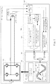
- FIG. 1 is a schematic diagram of a system frame for inverter with hysteresis control according to the present disclosure
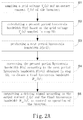
- FIG. 2A is a schematic diagram of a hysteresis control method for an inverter according to the present disclosure
- FIG. 2B is a schematic diagram of a hysteresis control method according to an embodiment of the present disclosure
- FIG. 3 is a diagram showing a relationship between the magnetic powder core inductance used in the inverter of embodiment of FIG. 2B and the current;
- FIG. 4 shows the hysteresis bandwidth with different inductances in the present invention, wherein the solid line shows waveform under a fixed inductance, and the broken line shows waveform under a changed inductance with the current (i.e., a varying inductance);
- FIG. 5 shows the waveforms of the theoretical hysteresis bandwidth calculated according to the bandwidth calculation formula and the actually discretized hysteresis bandwidth before the bandwidth correction;
- FIG. 6 is an enlarged view of waveform diagram near 0.01 s in FIG. 5 .
- FIG. 7 shows the deviation between the discretized hysteresis bandwidth and the theoretical hysteresis bandwidth in one period of FIG. 5 ;
- FIG. 8 shows the deviations of the actual hysteresis bandwidth and the theoretical hysteresis bandwidth in FIG. 5 from the theoretical hysteresis bandwidth
- FIG. 9 is an enlarged view of diagram of a hysteresis bandwidth near the zero crossing point according to an embodiment of the present disclosure.
- FIG. 10 is a schematic diagram showing the experimental results of current total harmonic distortion (THD) obtained by hysteresis control using the method of the present invention and a conventional method.
- TDD current total harmonic distortion
- the terms “include” and “comprise” are used in an open-ended fashion, and thus should be interpreted to mean “include, but not limited to.”
- the term “and/or” includes any and all combinations of one or more of the associated listed items.
- the term “coupled” may also be termed “electrically coupled,” and the term “connected” may be termed “electrically connected.” “Coupled” and “connected” may also be used to indicate that two or more elements cooperate or interact with each other. It will be understood that, although the terms “first,” “second,” etc., may be used herein to describe various elements, these elements should not be limited by these terms. These terms are used to distinguish one element from another. For example, a first element could be termed a second element, and, similarly, a second element could be termed a first element, without departing from the scope of the embodiments.
- FIG. 1 shows schematic diagram of the hysteresis control method for an inverter according to the present disclosure.
- the inverter with hysteresis control of the present disclosure includes a main power circuit 110 and a control module 120 .
- the main power circuit 110 has an input and an output, wherein the input is electrically connected to a DC bus, and the output is electrically connected to a power grid.
- the control module 120 is electrically connected to the main power circuit 110 and is used to control the main power circuit 110 to implement energy conversion from the input to the output.
- the control module 120 includes a sampling unit 121 , a bandwidth calculation unit 122 , a bandwidth prediction unit 123 , a correction unit 124 , and a main control unit 125 .
- the sampling unit 121 is configured to sample a grid voltage V g (z) and an output current I g (z) of the inverter.
- the bandwidth calculation unit 122 is configured to calculate a present period hysteresis bandwidth H(z) based on the grid voltage V g (z).
- the bandwidth prediction unit 123 is configured to predict a hysteresis next period bandwidth H(z+1).
- the correcting unit 124 is configured to correct the present period hysteresis bandwidth based on the next period hysteresis bandwidth H(z+1) to obtain a final hysteresis bandwidth H out (z).
- the main control unit 125 outputs driving signal S D based on the output current I g (z) and the final hysteresis bandwidth H out (z) to control the operation of the main power circuit 110 .
- the main control unit 125 sets a reference current value, and adds and subtracts half of the final hysteresis bandwidth H out (z)/2 based on the reference current value to obtain upper and lower limit values of the hysteresis, respectively.
- the main control unit 125 may further include a hysteresis comparator, which compares the sampled output current I g (z) with the upper limit and the lower limit of the hysteresis. For example, when the current increases to the upper limit, the driving signal S D of the corresponding switch tube is turned over, and the switch tube is turned off; when the current is reduced to the lower limit, the driving signal S D of the corresponding switch tube is turned over, and the switch tube is turned on. Thereby, the main control unit 125 outputs the driving signal S D to the main power circuit 110 to drive the main power circuit 110 for energy conversion.
- a hysteresis comparator which compares the sampled output current I g (z) with the upper limit and the lower limit of the hysteresis. For example, when the current increases to the upper limit, the driving signal S D of the corresponding switch tube is turned over, and the switch tube is turned off; when the current is reduced to the lower limit, the driving signal S D of the corresponding switch
- FIG. 2A shows the hysteresis control method for an inverter according to an embodiment of the present disclosure, which includes:
- Step S 1 sampling a grid voltage V g (z) and an output current I g (z) of the inverter;
- Step S 2 calculating a present period hysteresis bandwidth H(z) based on the grid voltage V g (z) sampled in step S 1 ;
- Step S 3 predicting the next period hysteresis bandwidth H(z+1);
- Step S 4 correcting the present period hysteresis bandwidth H(z) according to the next period hysteresis bandwidth H(z+1) obtained in step S 3 to obtain the final hysteresis bandwidth H out (z);
- Step S 5 outputting the driving signal according to the output current I g (z) and the final hysteresis bandwidth H out (z) to control the operation of the inverter.
- the so-called “period” may refer to interruption cycle in a digital control, which may also be a sampling cycle of the inverter, in which operations such as sampling, bandwidth setting, and the like can be completed.
- the hysteresis bandwidth can be calculated according to a conventional hysteresis bandwidth formula.
- the calculation formula of the hysteresis bandwidth differs with different topology and control of the inverter and the sequence of actions between the switching devices.
- the calculation formula of the hysteresis bandwidth may be
- the calculation formula of the hysteresis bandwidth may be:
- H is the hysteresis bandwidth
- L is the inductance of the inverter
- V g is the grid voltage
- V bus is the DC bus voltage
- f s is the switching frequency designed for the inverter.
- the present period hysteresis bandwidth H(z) can be calculated:
- H ⁇ ( z ) V g ⁇ ( z ) ⁇ ( V bus - V g ⁇ ( z ) ) V bus ⁇ L ⁇ f s
- H ⁇ ( z + 1 ) V g ⁇ ( z + 1 ) ⁇ ( V bus - V g ⁇ ( z + 1 ) ) V bus ⁇ L ⁇ f s
- the calculation method of hysteresis bandwidth is not limited to this case, and appropriate hysteresis bandwidth calculation formula can be adopted according to the actual situation of the inverter.
- the grid voltage V g (z) may be measured in real time, and substituted into the above calculation formula to calculate the hysteresis bandwidth H(z) of the present period.
- the next period hysteresis bandwidth H(z+1) can be obtained with method of online or offline according to an actual application situation. For example, if the requirement for the control accuracy is high, the bandwidth prediction unit 123 can predict the next period grid voltage V g (z+1) online, and calculate the next period hysteresis bandwidth H(z+1) according to the calculation formula of the hysteresis bandwidth. If the requirement for the control accuracy is low, the next period hysteresis bandwidth H(z+1) can be calculated by the bandwidth prediction unit 123 offline.
- H zero is the bandwidth value set near the zero crossing point.
- the method for online prediction can be used to predict the next period grid voltage V g (z+1).
- the offline mode is a method of calculating the theoretical control parameter in advance, wherein all the state parameters of the system are assumed to vary with the theoretical situation.
- the variables required for the next period calculation can be selected from the theoretical hysteresis bandwidth.
- the DC bus voltage V bus (z) can also be sampled in real time by the sampling unit 121 in step S 1 .
- the bandwidth calculation unit 122 calculates the present period hysteresis bandwidth H(z) based on the grid voltage V g (z) and the DC bus voltage V bus (z) sampled in step S 1 .
- the bandwidth prediction unit 123 predicts the next period grid voltage V g (z+1) and the next period DC bus voltage V bus (z+1) online, and calculates the next period hysteresis bandwidth H(z+1) based on the next period grid voltage V g (z+1) and the next period DC bus voltage V bus (z+1).
- the bandwidth prediction unit 123 can obtain the next period grid voltage V g (z+1) and the next period DC bus voltage V bus (z+1) offline, thereby calculating the next period hysteresis bandwidth H(z+1), wherein the calculation formula of the hysteresis bandwidth can also adopt the above Formula (1) or Formula (2), which will not be described in detail herein.
- the present period hysteresis bandwidth H(z) can be calculated:
- H ⁇ ( z ) V g ⁇ ( z ) ⁇ ( V bus ⁇ ( z ) - V g ⁇ ( z ) ) V bus ⁇ ( z ) ⁇ L ⁇ f s
- H ⁇ ( z + 1 ) V g ⁇ ( z + 1 ) ⁇ ( V bus ⁇ ( z + 1 ) - V g ⁇ ( z + 1 ) ) V bus ⁇ ( z + 1 ) ⁇ Lf s
- the correcting unit 124 may modify the present period hysteresis bandwidth H(z) by weighted average method.
- the final hysteresis bandwidth H out (z) may be calculated based on the present period hysteresis bandwidth H(z) and the next period hysteresis bandwidth H(z+1).
- the corrected formula of the final hysteresis bandwidth can be: H out ( z ) A ( z ) H ( z )+ B ( z ) H ( z+ 1),
- H out (z) is the final hysteresis bandwidth of the present period
- A(z) and B(z) are weight coefficients.
- the present disclosure can reduce the influence of discretization in digital control by taking the weighted average of the present period hysteresis bandwidth and the next period hysteresis bandwidth as the final hysteresis bandwidth.
- the inductance of the inverter in the calculation formula of the hysteresis bandwidth may be a fixed inductance.
- the inductance of the inverter in the calculation formula for the hysteresis bandwidth may be a varying inductance.
- the inductance of the inverter is not ideal, for example, when the inductance of the inductor formed by some materials (for example, the magnetic powder core) is affected greatly by current, the inductance of the inverter can be taken into consideration further to make the designed bandwidth more accurate.
- Step S 2 the method further includes:
- step S 20 wherein the bandwidth calculation unit 122 obtains the real time inductance L(z) of the inverter based on the output current I g (z) of the present period by the methods of looking up table or fitting curve.
- the method of looking up table is to search from a table containing different output current values of the inverter and corresponding inductances to obtain the real time inductance L(z) of the inverter corresponding to the output current I g (z) of the present period.
- Step S 3 the method includes:
- step S 30 wherein the bandwidth prediction unit 123 further predicts the next period output current I g (z+1) of the inverter, and obtains the next period inductance L(z+1) of the inverter by the looking up table method or the fitting curve method.
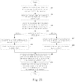
- the hysteresis control method for the inverter of the present disclosure will be further described in detail below with reference to FIG. 1 and FIG. 2B in an embodiment.
- the influence of discretization in the digital control and the influence of the inductance of the inverter are comprehensively considered.
- the hysteresis control method for the inverter of this embodiment includes:
- Step 201 sampling the grid voltage V g (z), the DC bus voltage V bus (z) and the output current I g (z) of the inverter;
- Step 202 obtaining the real time inductance L(z) of the inverter based on the output current I g (z).
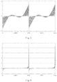
- FIG. 3 is a diagram showing relationship between the magnetic powder core inductance used in the inverter of embodiment of FIG. 2B and the current. It can be seen from FIG. 3 that the larger the current value, the smaller the inductance.
- FIG. 4 shows the theoretical bandwidth values with different inductances, wherein the solid line shows waveform under a fixed inductance, and the dashed line shows waveform under a varying inductance changed with the current. It can be seen from FIG. 4 that there is a significant deviation between the two results, thereby a more accurate hysteresis bandwidth can be obtained by considering the variation of the inductance during the design of the hysteresis bandwidth.
- Step 203 calculating the present period hysteresis bandwidth H(z) based on the sampled grid voltage V g (z), the DC bus voltage V bus (z), and the inductance L(z) of the inverter.
- the bandwidth calculation formula employed in the present embodiment is, for example, the Formula (1) or the Formula (2).
- the present period hysteresis bandwidth H(z) can be calculated:
- H ⁇ ( z ) V g ⁇ ( z ) ⁇ ( V bus ⁇ ( z ) - V g ⁇ ( z ) ) V bus ⁇ ( z ) ⁇ L ⁇ f s
- Step 204 according to the actual needs, selecting an online or offline method to obtain the next period hysteresis bandwidth H(z+1). If an online method is selected, then steps 205 and 206 are performed; if an offline method is selected, then steps 207 and 208 are performed.
- Step 205 predicting the variables required for the calculation of the next period hysteresis bandwidth H(z+1) online.
- the variables include, for example, the next period grid voltage V g (z+1), the next period DC bus voltage V bus (z+1), the next period inductance L(z+1), and etc. These variables can be obtained using existing prediction methods.
- Step 206 calculating the next period hysteresis bandwidth H(z+1).
- the bandwidth calculation formula of the next period corresponds to the calculation formula employed in step 203 .
- next period hysteresis bandwidth H(z+1) can be calculated:
- H ⁇ ( z + 1 ) V g ⁇ ( z + 1 ) ⁇ ( V bus ⁇ ( z + 1 ) - V g ⁇ ( z + 1 ) ) V bus ⁇ ( z + 1 ) ⁇ L ⁇ ( z + 1 ) ⁇ f s
- Step 207 calculating the variables required for the calculation of the next period hysteresis bandwidth offline.
- the variables include, for example, the next period grid voltage V g (z+1), the next period DC bus voltage V bus (z+1), the next period inductance L(z+1) and etc.
- Step 208 calculating the next period hysteresis bandwidth H(z+1) based on the variables calculated in step 207 .
- the calculation formula used to calculate the hysteresis bandwidth in this step is corresponding to the calculation formula used in step 203 .
- Step 209 taking the weight on the present period hysteresis bandwidth H(z) and the next period hysteresis bandwidth H(z+1) to calculate the final hysteresis bandwidth H out (z).
- the present period hysteresis bandwidth H(z) obtained in step 203 is weighted with the next period bandwidth H(z+1) calculated in step 206 or step 208 .
- the calculation formula is H out ( z ) A ( z ) H ( z )+ B ( z ) H ( z+ 1),
- H out (z) is the final hysteresis bandwidth of the present period
- Step 210 outputting a driving signal according to the output current I g (z) and the final hysteresis bandwidth H out (z) to control the operation of the inverter.
- the main control unit sets a reference current value, respectively adds and subtracts half of the final hysteresis bandwidth H out (z)/2, thereby calculating an upper limit of the hysteresis and a lower limit of the hysteresis, and compares the output current with the upper and lower limits of the hysteresis to finally output the driving signal to control the operation of the inverter.
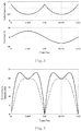
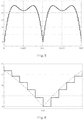
- FIG. 5 shows the waveforms of the theoretical hysteresis bandwidth calculated according to a bandwidth calculation formula and the actually discretized hysteresis bandwidth before the bandwidth correction, wherein the dashed line shows the theoretical values and the solid line shows the discretized bandwidth in the digital control.
- FIG. 6 is an enlarged view of waveform diagram near 0.01 s in FIG. 5 , in which there is a significant deviation between the solid line and the broken line, which means discretized bandwidth are not equal to theoretical values.
- FIG. 7 shows the deviation between the discretized bandwidth and the theoretical bandwidth in one power frequency period, and it can be clearly seen that the deviation is largest near the zero crossing point.
- FIG. 8 shows the proportion of the deviation in the theoretical bandwidth. According to FIG. 8 , the digital discretization results in a very large deviation near the zero crossing point, which will cause severe distortion of the current.
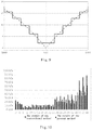
- FIG. 9 is an enlarged view of diagram showing the result of the bandwidth calculation of the present embodiment near the zero crossing point. Comparing FIG. 9 with FIG. 6 , it can be seen that the discretization deviation is corrected.
- FIG. 10 is a schematic diagram showing experimental results of current Total Harmonic Distortion (THD) obtained by hysteresis control using the method of the present disclosure and a conventional method, wherein white stripe blocks represent experimental results by a conventional hysteresis control method, and black squares represent the experimental results by the hysteresis control method of the present disclosure.
- TDD Total Harmonic Distortion
Landscapes
- Engineering & Computer Science (AREA)
- Power Engineering (AREA)
- Inverter Devices (AREA)
Abstract
Description
H out(z)A(z)H(z)+B(z)H(z+1),
H out(z)A(z)H(z)+B(z)H(z+1),
Claims (26)
H out(z)=A(z)H(z)+B(z)H(z+1),
H out(z)=A(z)H(z)+B(z)H(z+1),
Applications Claiming Priority (3)
| Application Number | Priority Date | Filing Date | Title |
|---|---|---|---|
| CN201910040236.0 | 2019-01-16 | ||
| CN201910040236.0A CN111446876B (en) | 2019-01-16 | 2019-01-16 | Hysteresis control method of inverter and inverter based on hysteresis control |
| CN201910040236 | 2019-01-16 |
Publications (2)
| Publication Number | Publication Date |
|---|---|
| US20200228102A1 US20200228102A1 (en) | 2020-07-16 |
| US10897241B2 true US10897241B2 (en) | 2021-01-19 |
Family
ID=71516943
Family Applications (1)
| Application Number | Title | Priority Date | Filing Date |
|---|---|---|---|
| US16/718,104 Active US10897241B2 (en) | 2019-01-16 | 2019-12-17 | Hysteresis control method for inverter and an inverter with hysteresis control |
Country Status (2)
| Country | Link |
|---|---|
| US (1) | US10897241B2 (en) |
| CN (1) | CN111446876B (en) |
Citations (10)
| Publication number | Priority date | Publication date | Assignee | Title |
|---|---|---|---|---|
| CN103280808A (en) | 2013-06-08 | 2013-09-04 | 南京因泰莱电器股份有限公司 | Variable ring width hysteresis current control method based on timer |
| CN103684008A (en) | 2013-12-13 | 2014-03-26 | 安徽大学 | Control method of current hysteresis inverter |
| US20140112039A1 (en) * | 2011-07-04 | 2014-04-24 | Sma Solar Technology Ag | Operating method for an inverter and grid fault tolerant inverter |
| US20140169053A1 (en) * | 2011-12-16 | 2014-06-19 | Milan Ilic | Distributed voltage source inverters |
| US8780592B1 (en) * | 2011-07-11 | 2014-07-15 | Chilicon Power, LLC | Systems and methods for increasing output current quality, output power, and reliability of grid-interactive inverters |
| US20150070956A1 (en) * | 2013-09-09 | 2015-03-12 | Fsp-Powerland Technology Inc. | Inverter and direct current bus voltage regulating method thereof and application using the same |
| US20150288220A1 (en) * | 2014-04-07 | 2015-10-08 | Bloom Energy Corporation | Parallel Control of Multiple Uninterruptable Power Modules ("UPMs") |
| CN105871241A (en) * | 2016-04-07 | 2016-08-17 | 西安交通大学 | Sampling period online prediction-based fixed switching frequency digital hysteresis control method |
| US9843272B2 (en) * | 2013-04-04 | 2017-12-12 | Toshiba Mitsubishi-Electric Industrial Systems Corporation | Power converter capable of outputting a plurality of different levels of voltages |
| US20180145582A1 (en) * | 2017-01-16 | 2018-05-24 | Hunan University | Virtual synchronous inverter with fast transient inrush fault currents restraining method thereof |
-
2019
- 2019-01-16 CN CN201910040236.0A patent/CN111446876B/en active Active
- 2019-12-17 US US16/718,104 patent/US10897241B2/en active Active
Patent Citations (12)
| Publication number | Priority date | Publication date | Assignee | Title |
|---|---|---|---|---|
| US20140112039A1 (en) * | 2011-07-04 | 2014-04-24 | Sma Solar Technology Ag | Operating method for an inverter and grid fault tolerant inverter |
| US8780592B1 (en) * | 2011-07-11 | 2014-07-15 | Chilicon Power, LLC | Systems and methods for increasing output current quality, output power, and reliability of grid-interactive inverters |
| US20140169053A1 (en) * | 2011-12-16 | 2014-06-19 | Milan Ilic | Distributed voltage source inverters |
| US9843272B2 (en) * | 2013-04-04 | 2017-12-12 | Toshiba Mitsubishi-Electric Industrial Systems Corporation | Power converter capable of outputting a plurality of different levels of voltages |
| CN103280808A (en) | 2013-06-08 | 2013-09-04 | 南京因泰莱电器股份有限公司 | Variable ring width hysteresis current control method based on timer |
| CN103280808B (en) | 2013-06-08 | 2015-05-20 | 南京因泰莱电器股份有限公司 | Variable ring width hysteresis current control method based on timer |
| US20150070956A1 (en) * | 2013-09-09 | 2015-03-12 | Fsp-Powerland Technology Inc. | Inverter and direct current bus voltage regulating method thereof and application using the same |
| CN103684008A (en) | 2013-12-13 | 2014-03-26 | 安徽大学 | Control method of current hysteresis inverter |
| CN103684008B (en) | 2013-12-13 | 2016-03-16 | 安徽大学 | A kind of Hysteresis Current inverter control method |
| US20150288220A1 (en) * | 2014-04-07 | 2015-10-08 | Bloom Energy Corporation | Parallel Control of Multiple Uninterruptable Power Modules ("UPMs") |
| CN105871241A (en) * | 2016-04-07 | 2016-08-17 | 西安交通大学 | Sampling period online prediction-based fixed switching frequency digital hysteresis control method |
| US20180145582A1 (en) * | 2017-01-16 | 2018-05-24 | Hunan University | Virtual synchronous inverter with fast transient inrush fault currents restraining method thereof |
Also Published As
| Publication number | Publication date |
|---|---|
| CN111446876A (en) | 2020-07-24 |
| CN111446876B (en) | 2021-03-19 |
| US20200228102A1 (en) | 2020-07-16 |
Similar Documents
| Publication | Publication Date | Title |
|---|---|---|
| TWI445292B (en) | Mid-voltage variable-frequency driving system and total harmonic distortion compensation method | |
| US11855460B2 (en) | Photovoltaic inverter and corresponding switching frequency control method | |
| Long et al. | Ultralocal model-free predictive control of T-type grid-connected converters based on extended sliding-mode disturbance observer | |
| JP5343230B2 (en) | Inverter | |
| EP3320609B1 (en) | Control of electrical converter based on optimized pulse patterns | |
| EP2114002A1 (en) | 3-phase power conversion device | |
| Monteiro et al. | Experimental validation of a proposed single-phase five-level active rectifier operating with model predictive current control | |
| US10666131B2 (en) | Dead-time voltage compensation apparatus and dead-time voltage compensation method | |
| US10897241B2 (en) | Hysteresis control method for inverter and an inverter with hysteresis control | |
| JP2019154209A (en) | Dc/dc converter control device | |
| CN100440709C (en) | Variable Coefficient Control Method of Rectifier | |
| CN109088561B (en) | A Load Current Predictive Feedforward Control Method | |
| Yin et al. | A triple-voltage-vector model-free predictive current control scheme for voltage source inverters | |
| WO2019097835A1 (en) | Power conversion device | |
| KR20240111247A (en) | Controlling apparatus and method for 3 phase voltage source inverters | |
| KR20170137272A (en) | Current Control Methods for Single-Phase Voltage Source Inverters | |
| CN113937816A (en) | Self-adaptive efficient robust stable control device for comprehensive power supply | |
| Khamooshi et al. | Comprehensive harmonic optimization in cascaded h-bridge multilevel inverters using variable DC sources | |
| Defay et al. | Predictive control of flying capacitor active power filter | |
| CN121546912B (en) | ZVT-Boost PFC circuit with saturation inductance | |
| Kurokawa et al. | A new high performance DC-DC converter with sensorless model reference modification | |
| CN113809948B (en) | A feedback current compensation method for grid-connected inverters under shunt sampling current conditions | |
| JP2013188007A (en) | Power converter | |
| CN112701722B (en) | Active damping method for inhibiting grid-connected current dead zone harmonic of energy router | |
| Abdullah | Model Predictive Control for Power Quality Enhancement in Grid-Tied Renewable Energy Inverters |
Legal Events
| Date | Code | Title | Description |
|---|---|---|---|
| FEPP | Fee payment procedure |
Free format text: ENTITY STATUS SET TO UNDISCOUNTED (ORIGINAL EVENT CODE: BIG.); ENTITY STATUS OF PATENT OWNER: LARGE ENTITY |
|
| AS | Assignment |
Owner name: DELTA ELECTRONICS (SHANGHAI) CO.,LTD., CHINA Free format text: ASSIGNMENT OF ASSIGNORS INTEREST;ASSIGNORS:WEI, QIKANG;XU, FEIDONG;ZHU, XUANCAI;REEL/FRAME:051311/0286 Effective date: 20191108 |
|
| STPP | Information on status: patent application and granting procedure in general |
Free format text: NOTICE OF ALLOWANCE MAILED -- APPLICATION RECEIVED IN OFFICE OF PUBLICATIONS |
|
| STPP | Information on status: patent application and granting procedure in general |
Free format text: PUBLICATIONS -- ISSUE FEE PAYMENT VERIFIED |
|
| STCF | Information on status: patent grant |
Free format text: PATENTED CASE |
|
| MAFP | Maintenance fee payment |
Free format text: PAYMENT OF MAINTENANCE FEE, 4TH YEAR, LARGE ENTITY (ORIGINAL EVENT CODE: M1551); ENTITY STATUS OF PATENT OWNER: LARGE ENTITY Year of fee payment: 4 |