US10896853B2 - Mask-free methods of forming structures in a semiconductor device - Google Patents
Mask-free methods of forming structures in a semiconductor device Download PDFInfo
- Publication number
- US10896853B2 US10896853B2 US16/396,775 US201916396775A US10896853B2 US 10896853 B2 US10896853 B2 US 10896853B2 US 201916396775 A US201916396775 A US 201916396775A US 10896853 B2 US10896853 B2 US 10896853B2
- Authority
- US
- United States
- Prior art keywords
- layer
- wfm
- semiconductor device
- cavity
- material layer
- Prior art date
- Legal status (The legal status is an assumption and is not a legal conclusion. Google has not performed a legal analysis and makes no representation as to the accuracy of the status listed.)
- Active
Links
Images


Classifications
-
- H01L21/823456—
-
- H01L21/28568—
-
- H01L21/30604—
-
- H01L21/3065—
-
- H01L21/32134—
-
- H01L21/32135—
-
- H01L27/088—
-
- H01L29/42372—
-
- H—ELECTRICITY
- H10—SEMICONDUCTOR DEVICES; ELECTRIC SOLID-STATE DEVICES NOT OTHERWISE PROVIDED FOR
- H10D—INORGANIC ELECTRIC SEMICONDUCTOR DEVICES
- H10D64/00—Electrodes of devices having potential barriers
- H10D64/01—Manufacture or treatment
- H10D64/017—Manufacture or treatment using dummy gates in processes wherein at least parts of the final gates are self-aligned to the dummy gates, i.e. replacement gate processes
-
- H—ELECTRICITY
- H10—SEMICONDUCTOR DEVICES; ELECTRIC SOLID-STATE DEVICES NOT OTHERWISE PROVIDED FOR
- H10D—INORGANIC ELECTRIC SEMICONDUCTOR DEVICES
- H10D64/00—Electrodes of devices having potential barriers
- H10D64/20—Electrodes characterised by their shapes, relative sizes or dispositions
- H10D64/27—Electrodes not carrying the current to be rectified, amplified, oscillated or switched, e.g. gates
- H10D64/311—Gate electrodes for field-effect devices
- H10D64/411—Gate electrodes for field-effect devices for FETs
- H10D64/511—Gate electrodes for field-effect devices for FETs for IGFETs
- H10D64/517—Gate electrodes for field-effect devices for FETs for IGFETs characterised by the conducting layers
-
- H—ELECTRICITY
- H10—SEMICONDUCTOR DEVICES; ELECTRIC SOLID-STATE DEVICES NOT OTHERWISE PROVIDED FOR
- H10D—INORGANIC ELECTRIC SEMICONDUCTOR DEVICES
- H10D64/00—Electrodes of devices having potential barriers
- H10D64/60—Electrodes characterised by their materials
- H10D64/66—Electrodes having a conductor capacitively coupled to a semiconductor by an insulator, e.g. MIS electrodes
- H10D64/667—Electrodes having a conductor capacitively coupled to a semiconductor by an insulator, e.g. MIS electrodes the conductor comprising a layer of alloy material, compound material or organic material contacting the insulator, e.g. TiN workfunction layers
-
- H—ELECTRICITY
- H10—SEMICONDUCTOR DEVICES; ELECTRIC SOLID-STATE DEVICES NOT OTHERWISE PROVIDED FOR
- H10D—INORGANIC ELECTRIC SEMICONDUCTOR DEVICES
- H10D84/00—Integrated devices formed in or on semiconductor substrates that comprise only semiconducting layers, e.g. on Si wafers or on GaAs-on-Si wafers
- H10D84/01—Manufacture or treatment
- H10D84/0123—Integrating together multiple components covered by H10D12/00 or H10D30/00, e.g. integrating multiple IGBTs
- H10D84/0126—Integrating together multiple components covered by H10D12/00 or H10D30/00, e.g. integrating multiple IGBTs the components including insulated gates, e.g. IGFETs
- H10D84/0135—Manufacturing their gate conductors
- H10D84/0142—Manufacturing their gate conductors the gate conductors having different shapes or dimensions
-
- H—ELECTRICITY
- H10—SEMICONDUCTOR DEVICES; ELECTRIC SOLID-STATE DEVICES NOT OTHERWISE PROVIDED FOR
- H10D—INORGANIC ELECTRIC SEMICONDUCTOR DEVICES
- H10D84/00—Integrated devices formed in or on semiconductor substrates that comprise only semiconducting layers, e.g. on Si wafers or on GaAs-on-Si wafers
- H10D84/01—Manufacture or treatment
- H10D84/02—Manufacture or treatment characterised by using material-based technologies
- H10D84/03—Manufacture or treatment characterised by using material-based technologies using Group IV technology, e.g. silicon technology or silicon-carbide [SiC] technology
- H10D84/038—Manufacture or treatment characterised by using material-based technologies using Group IV technology, e.g. silicon technology or silicon-carbide [SiC] technology using silicon technology, e.g. SiGe
-
- H—ELECTRICITY
- H10—SEMICONDUCTOR DEVICES; ELECTRIC SOLID-STATE DEVICES NOT OTHERWISE PROVIDED FOR
- H10D—INORGANIC ELECTRIC SEMICONDUCTOR DEVICES
- H10D84/00—Integrated devices formed in or on semiconductor substrates that comprise only semiconducting layers, e.g. on Si wafers or on GaAs-on-Si wafers
- H10D84/80—Integrated devices formed in or on semiconductor substrates that comprise only semiconducting layers, e.g. on Si wafers or on GaAs-on-Si wafers characterised by the integration of at least one component covered by groups H10D12/00 or H10D30/00, e.g. integration of IGFETs
- H10D84/82—Integrated devices formed in or on semiconductor substrates that comprise only semiconducting layers, e.g. on Si wafers or on GaAs-on-Si wafers characterised by the integration of at least one component covered by groups H10D12/00 or H10D30/00, e.g. integration of IGFETs of only field-effect components
- H10D84/83—Integrated devices formed in or on semiconductor substrates that comprise only semiconducting layers, e.g. on Si wafers or on GaAs-on-Si wafers characterised by the integration of at least one component covered by groups H10D12/00 or H10D30/00, e.g. integration of IGFETs of only field-effect components of only insulated-gate FETs [IGFET]
-
- H—ELECTRICITY
- H10—SEMICONDUCTOR DEVICES; ELECTRIC SOLID-STATE DEVICES NOT OTHERWISE PROVIDED FOR
- H10P—GENERIC PROCESSES OR APPARATUS FOR THE MANUFACTURE OR TREATMENT OF DEVICES COVERED BY CLASS H10
- H10P14/00—Formation of materials, e.g. in the shape of layers or pillars
- H10P14/40—Formation of materials, e.g. in the shape of layers or pillars of conductive or resistive materials
- H10P14/418—Formation of materials, e.g. in the shape of layers or pillars of conductive or resistive materials the conductive layers comprising transition metals
-
- H—ELECTRICITY
- H10—SEMICONDUCTOR DEVICES; ELECTRIC SOLID-STATE DEVICES NOT OTHERWISE PROVIDED FOR
- H10P—GENERIC PROCESSES OR APPARATUS FOR THE MANUFACTURE OR TREATMENT OF DEVICES COVERED BY CLASS H10
- H10P50/00—Etching of wafers, substrates or parts of devices
- H10P50/20—Dry etching; Plasma etching; Reactive-ion etching
- H10P50/24—Dry etching; Plasma etching; Reactive-ion etching of semiconductor materials
- H10P50/242—Dry etching; Plasma etching; Reactive-ion etching of semiconductor materials of Group IV materials
-
- H—ELECTRICITY
- H10—SEMICONDUCTOR DEVICES; ELECTRIC SOLID-STATE DEVICES NOT OTHERWISE PROVIDED FOR
- H10P—GENERIC PROCESSES OR APPARATUS FOR THE MANUFACTURE OR TREATMENT OF DEVICES COVERED BY CLASS H10
- H10P50/00—Etching of wafers, substrates or parts of devices
- H10P50/20—Dry etching; Plasma etching; Reactive-ion etching
- H10P50/26—Dry etching; Plasma etching; Reactive-ion etching of conductive or resistive materials
- H10P50/264—Dry etching; Plasma etching; Reactive-ion etching of conductive or resistive materials by chemical means
- H10P50/266—Dry etching; Plasma etching; Reactive-ion etching of conductive or resistive materials by chemical means by vapour etching only
-
- H—ELECTRICITY
- H10—SEMICONDUCTOR DEVICES; ELECTRIC SOLID-STATE DEVICES NOT OTHERWISE PROVIDED FOR
- H10P—GENERIC PROCESSES OR APPARATUS FOR THE MANUFACTURE OR TREATMENT OF DEVICES COVERED BY CLASS H10
- H10P50/00—Etching of wafers, substrates or parts of devices
- H10P50/60—Wet etching
- H10P50/64—Wet etching of semiconductor materials
- H10P50/642—Chemical etching
-
- H—ELECTRICITY
- H10—SEMICONDUCTOR DEVICES; ELECTRIC SOLID-STATE DEVICES NOT OTHERWISE PROVIDED FOR
- H10P—GENERIC PROCESSES OR APPARATUS FOR THE MANUFACTURE OR TREATMENT OF DEVICES COVERED BY CLASS H10
- H10P50/00—Etching of wafers, substrates or parts of devices
- H10P50/60—Wet etching
- H10P50/66—Wet etching of conductive or resistive materials
- H10P50/663—Wet etching of conductive or resistive materials by chemical means only
- H10P50/667—Wet etching of conductive or resistive materials by chemical means only by liquid etching only
-
- H—ELECTRICITY
- H10—SEMICONDUCTOR DEVICES; ELECTRIC SOLID-STATE DEVICES NOT OTHERWISE PROVIDED FOR
- H10D—INORGANIC ELECTRIC SEMICONDUCTOR DEVICES
- H10D84/00—Integrated devices formed in or on semiconductor substrates that comprise only semiconducting layers, e.g. on Si wafers or on GaAs-on-Si wafers
- H10D84/01—Manufacture or treatment
- H10D84/0123—Integrating together multiple components covered by H10D12/00 or H10D30/00, e.g. integrating multiple IGBTs
- H10D84/0126—Integrating together multiple components covered by H10D12/00 or H10D30/00, e.g. integrating multiple IGBTs the components including insulated gates, e.g. IGFETs
- H10D84/0135—Manufacturing their gate conductors
- H10D84/014—Manufacturing their gate conductors the gate conductors having different materials or different implants
-
- H—ELECTRICITY
- H10—SEMICONDUCTOR DEVICES; ELECTRIC SOLID-STATE DEVICES NOT OTHERWISE PROVIDED FOR
- H10D—INORGANIC ELECTRIC SEMICONDUCTOR DEVICES
- H10D84/00—Integrated devices formed in or on semiconductor substrates that comprise only semiconducting layers, e.g. on Si wafers or on GaAs-on-Si wafers
- H10D84/01—Manufacture or treatment
- H10D84/0123—Integrating together multiple components covered by H10D12/00 or H10D30/00, e.g. integrating multiple IGBTs
- H10D84/0126—Integrating together multiple components covered by H10D12/00 or H10D30/00, e.g. integrating multiple IGBTs the components including insulated gates, e.g. IGFETs
- H10D84/0158—Integrating together multiple components covered by H10D12/00 or H10D30/00, e.g. integrating multiple IGBTs the components including insulated gates, e.g. IGFETs the components including FinFETs
-
- H—ELECTRICITY
- H10—SEMICONDUCTOR DEVICES; ELECTRIC SOLID-STATE DEVICES NOT OTHERWISE PROVIDED FOR
- H10D—INORGANIC ELECTRIC SEMICONDUCTOR DEVICES
- H10D84/00—Integrated devices formed in or on semiconductor substrates that comprise only semiconducting layers, e.g. on Si wafers or on GaAs-on-Si wafers
- H10D84/80—Integrated devices formed in or on semiconductor substrates that comprise only semiconducting layers, e.g. on Si wafers or on GaAs-on-Si wafers characterised by the integration of at least one component covered by groups H10D12/00 or H10D30/00, e.g. integration of IGFETs
- H10D84/82—Integrated devices formed in or on semiconductor substrates that comprise only semiconducting layers, e.g. on Si wafers or on GaAs-on-Si wafers characterised by the integration of at least one component covered by groups H10D12/00 or H10D30/00, e.g. integration of IGFETs of only field-effect components
- H10D84/83—Integrated devices formed in or on semiconductor substrates that comprise only semiconducting layers, e.g. on Si wafers or on GaAs-on-Si wafers characterised by the integration of at least one component covered by groups H10D12/00 or H10D30/00, e.g. integration of IGFETs of only field-effect components of only insulated-gate FETs [IGFET]
- H10D84/834—Integrated devices formed in or on semiconductor substrates that comprise only semiconducting layers, e.g. on Si wafers or on GaAs-on-Si wafers characterised by the integration of at least one component covered by groups H10D12/00 or H10D30/00, e.g. integration of IGFETs of only field-effect components of only insulated-gate FETs [IGFET] comprising FinFETs
-
- H—ELECTRICITY
- H10—SEMICONDUCTOR DEVICES; ELECTRIC SOLID-STATE DEVICES NOT OTHERWISE PROVIDED FOR
- H10D—INORGANIC ELECTRIC SEMICONDUCTOR DEVICES
- H10D86/00—Integrated devices formed in or on insulating or conducting substrates, e.g. formed in silicon-on-insulator [SOI] substrates or on stainless steel or glass substrates
- H10D86/01—Manufacture or treatment
- H10D86/011—Manufacture or treatment comprising FinFETs
-
- H—ELECTRICITY
- H10—SEMICONDUCTOR DEVICES; ELECTRIC SOLID-STATE DEVICES NOT OTHERWISE PROVIDED FOR
- H10D—INORGANIC ELECTRIC SEMICONDUCTOR DEVICES
- H10D86/00—Integrated devices formed in or on insulating or conducting substrates, e.g. formed in silicon-on-insulator [SOI] substrates or on stainless steel or glass substrates
- H10D86/201—Integrated devices formed in or on insulating or conducting substrates, e.g. formed in silicon-on-insulator [SOI] substrates or on stainless steel or glass substrates the substrates comprising an insulating layer on a semiconductor body, e.g. SOI
- H10D86/215—Integrated devices formed in or on insulating or conducting substrates, e.g. formed in silicon-on-insulator [SOI] substrates or on stainless steel or glass substrates the substrates comprising an insulating layer on a semiconductor body, e.g. SOI comprising FinFETs
-
- H—ELECTRICITY
- H10—SEMICONDUCTOR DEVICES; ELECTRIC SOLID-STATE DEVICES NOT OTHERWISE PROVIDED FOR
- H10P—GENERIC PROCESSES OR APPARATUS FOR THE MANUFACTURE OR TREATMENT OF DEVICES COVERED BY CLASS H10
- H10P50/00—Etching of wafers, substrates or parts of devices
- H10P50/71—Etching of wafers, substrates or parts of devices using masks for conductive or resistive materials
Definitions
- the present disclosure generally relates to semiconductor device fabrication and integrated circuits. More particularly, the present disclosure relates to replacement metal gate processes and structures for transistor devices having a short channel and a long channel component. The present disclosure also relates to processes and structures for multi-gates with dissimilar threshold voltages.
- transistor device architectures such as three-dimensional (3D) fin-shaped field effect transistors (FinFETs), and planar transistor devices built on bulk substrates or substrates with a buried insulator layer (i.e., semiconductor-on-insulator device).
- FinFETs three-dimensional fin-shaped field effect transistors
- device architectures typically include a substrate, an active region, and a gate electrode.
- the active region may contain electrical input and output contacts and functions as a channel for current flow.
- the gate electrode is typically placed above the channel and controls the flow of current therein. Multiple gate electrodes may also be formed over an active region to enable variability of current flow across device elements. Variability of the current flow in the channel region may be controlled by adjusting the threshold voltage property of a device. The threshold voltage may be adjusted by modifying various characteristics/features of the gate electrode and the channel beneath the gate, such as the work-function portion of a gate, the gate dielectric portion, the dopant concentration of the channel, the length of the channel, and the types of materials used in the gate electrode.
- a common approach to fabricate multiple gate electrodes that provide different threshold voltages in a device is to utilize photolithographic technologies and masks, including reticle masks, optical masks and photolithographic masks. These masks enable the creation of various patterns over a substrate, which in turn enables the modification of desired features in a gate electrode (e.g., the thicknesses/material composition of the work-function portion in a gate), thereby allowing adjustments to the threshold voltage property of the device.
- desired features in a gate electrode e.g., the thicknesses/material composition of the work-function portion in a gate
- the use of masks and the associated photolithographic tools incur significantly large monetary costs and are undesirable in a competitive business environment.
- a method of forming structures in a semiconductor device by forming first and second cavities having sidewalls and bottom surfaces in a dielectric structure, where the first cavity has a narrower opening than the second cavity, forming a first material layer in the first and second cavities, forming a protective layer over the first material layer, where the protective layer fills the first cavity and conformally covers the sidewall and the bottom surfaces of the second cavity, performing a first isotropic etch on the protective layer to selectively remove a portion of the protective layer and form a retained portion of the protective layer, performing a second isotropic etch on the first material layer to selectively remove a portion of the first material layer and form a retained portion of the first material layer, removing the retained portion of the protective layer, and forming a second material layer in the first and second cavities, the second material layer being formed on the retained portion of the first material layer.
- a method of forming gate structures in a semiconductor device by forming first and second gate cavities having sidewall surfaces and bottom surfaces, the first and second gate cavities being formed above an active region and separated by a dielectric structure, where the first gate cavity has a shorter channel length than the second gate cavity, forming a first work-function material (WFM) layer in the first and second gate cavities, forming a protective layer over the first WFM layer, where the protective layer fills the first gate cavity and conformally covers the sidewall and the bottom surfaces of the second gate cavity, performing a first isotropic etch on the protective layer to selectively remove a portion of the protective layer and form a retained portion of the protective layer, performing a second isotropic etch on the first WFM layer to selectively remove a portion of the first WFM layer and form a retained portion of the first WFM layer, removing the retained portion of the protective layer, and forming a second WFM layer in the first and second cavities, the second WFM layer being formed on the retained portion of the
- a semiconductor device including first and second structures separated by a dielectric structure formed above an active region, the first and second structures having sidewall and bottom surfaces, where the bottom surface of the first structure is smaller than the bottom surface of the second structure, a dielectric layer disposed on the sidewall and the bottom surfaces of the first and second structures, and a work-function material (WFM) layer disposed on the dielectric layers in either the first structure or the second structure.
- WFM work-function material
- FIGS. 1A and 1B are cross-sectional and plan views, respectively, of a set of device features for forming structures in a semiconductor device in accordance with embodiments of the present disclosure.
- FIGS. 2 to 4 are cross-sectional views depicting successive stages of forming structures in a semiconductor device in accordance with embodiments of the present disclosure.
- FIGS. 5 to 8 are cross-sectional views depicting, in successive stages, an exemplary set of diagrams for forming structures in a semiconductor device in accordance with embodiments of the present disclosure.
- FIGS. 9 to 15 are cross-sectional views depicting, in successive stages, another exemplary set of diagrams for forming structures in a semiconductor device in accordance with embodiments of the present disclosure.
- FIGS. 1A and 1B a cross-sectional view and a plan view, respectively, show a set of device features for forming a semiconductor structure in accordance with the present disclosure.
- the device features may include a substrate (not shown in the accompanying drawings), an active region 104 (e.g., a fin) formed on the substrate, and first and second cavities ( 108 a and 108 b , respectively) disposed above and extending laterally across the active region 104 .
- the active region 104 includes a channel region flanked by a source contact and a drain contact.
- the device features may be formed by conventional semiconductor fabrication processes.
- the first and second cavities ( 108 a and 108 b , respectively) may be used for device features that are formed at various fabrication stages (e.g., front-end of line, middle-end of line, or back-end of line processes).
- the first and second cavities ( 108 a and 108 b , respectively) may be device features such as interconnect via openings, gate cut trenches, or gate cavities.
- the first and second cavities ( 108 a and 108 b , respectively) are gate cavities formed after the removal of dummy gate electrodes during replacement metal gate processes.
- the first and second cavities may be separated or electrically isolated from each other by a dielectric structure 106 .
- the dielectric structure 106 may include a dielectric compound, such as silicon nitride (SiN), or silicon dioxide (SiO 2 ). Additionally, the first and second cavities ( 108 a and 108 b , respectively) may be flanked by sidewall spacer structures 110 , and an interfacial dielectric layer 112 (e.g., silicon dioxide (SiO 2 )) is formed at the bottom of the cavities. As shown in FIG.
- the lined first and second cavities ( 108 a and 108 b , respectively) have sidewall surfaces 120 a and 120 b , and bottom surfaces 122 a and 122 b .
- the bottom surface 122 a of the first cavity 108 a is smaller than the bottom surface 122 b of the second cavity 108 b.
- the sidewall spacer structures 110 may function as a gate spacer to prevent an electrical short between the gate electrode and the source/drain regions in the active region 104 .
- the sidewall spacer structures 110 may include a low-K dielectric material.
- low-K refers to a material having a dielectric constant (i.e., K value) that is lower than 7.
- Exemplary low-K dielectric material may include, but not limited to, silicon dioxide (SiO 2 ), silicon oxide materials enriched or doped with atomic elements selected from the group consisting of carbon, boron, hydrogen and nitrogen (e.g., SiOCN, SiBCN), silicon oxynitride (SiON), SiGe oxide, germanium oxide, silicon oxycarbide, SiCOH dielectrics, or any combination thereof.
- SiO 2 silicon dioxide
- SiO 2 silicon oxide materials enriched or doped with atomic elements selected from the group consisting of carbon, boron, hydrogen and nitrogen (e.g., SiOCN, SiBCN), silicon oxynitride (SiON), SiGe oxide, germanium oxide, silicon oxycarbide, SiCOH dielectrics, or any combination thereof.
- the first cavity 108 a has a width dimension 102 a in the range of about 16 nm to about 30 nm, while the second cavity 108 b has a width dimension 102 b in the range of about 30 nm to about 300 nm.
- the width 102 a of the first cavity 108 a may be smaller than the width 102 b of the second cavity 108 b .
- the first cavity width 102 a and the second cavity width 102 b differ from each other in the range of about 40 nm to about 280 nm.
- the width dimensions 102 a and 102 b correspond to the lengths of the channels below gate electrodes.
- the first gate cavity 108 a has a shorter channel length than the second gate cavity 108 b.
- FIG. 1B shows the plan view for the set of device features depicted in FIG. 1A .
- the line X-X′ indicates the position of a section line for the cross-sectional view shown in FIG. 1A .
- the dielectric structure 106 is omitted so as not to obscure the illustration of active regions 104 positioned underneath.
- the active region 104 is represented as a fin in the accompanying drawings, it should be noted that the fin is used only as a non-limiting example of the active region 104 , and other active regions (e.g., a doped layer on a top surface of a bulk semiconductor substrate or a semiconductor-on-insulator layer) may be used as well. It should also be understood that the present disclosure can be applied to any type of transistor device architecture, such as a three-dimensional device architecture (e.g., FinFETs), or a planar device architecture (e.g., complementary metal oxide semiconductor (CMOS) devices), semiconductor-on-insulator (SOI) devices).
- CMOS complementary metal oxide semiconductor
- SOI semiconductor-on-insulator
- the active region 104 may be made of any suitable semiconductor material, such as silicon, germanium, or silicon germanium.
- the substrate may be made of any suitable semiconductor material, such as silicon (Si), germanium (Ge), silicon germanium (SiGe), silicon/carbon, other II-VI or III-V semiconductor compounds and the like.
- the substrate may also include an organic semiconductor or a layered semiconductor, such as Si/SiGe, a silicon-on-insulator or a SiGe-on-insulator.
- a dielectric layer 114 is formed in the first and second cavities ( 108 a and 108 b , respectively).
- the dielectric layer 114 may be formed by conventional deposition processes, such as chemical vapor deposition (CVD), physical vapor deposition (PVD), molecular beam deposition (MBD), pulsed laser deposition (PLD), liquid source misted chemical deposition (LSMCD), atomic layer deposition (ALD), etc.
- CVD chemical vapor deposition
- PVD physical vapor deposition
- MBD molecular beam deposition
- PLD pulsed laser deposition
- LSMCD liquid source misted chemical deposition
- ALD atomic layer deposition
- a highly conformal deposition process is preferred for depositing the dielectric layer 114 ; for example, an ALD process or a highly-controlled CVD process. As shown in FIG.
- the dielectric layer 114 is deposited on and conforming to the sidewall surfaces 120 a and 120 b and the bottom surfaces 122 a and 122 b . In addition, the dielectric layer 114 is formed on a top surface 132 of the dielectric structure 106 .
- the dielectric layer 114 is a gate dielectric layer having a high-K dielectric material.
- high-K refers to a material having a dielectric constant (i.e., K value) that is greater than 7.
- the high-K dielectric material may include, but not limited to, hafnium oxide (HfO 2 ), zirconium oxide (ZrO 2 ), lanthanum oxide (La 2 O 3 ), aluminum oxide (Al 2 O 3 ), titanium oxide (TiO 2 ), strontium titanium oxide (SrTiO 3 ), lanthanum aluminum oxide (LaAlO 3 ), yttrium oxide (Y 2 O 3 ), hafnium oxynitride (HfO x N y ), zirconium oxynitride (ZrO x N y ), lanthanum oxynitride (La 2 O x N y ), aluminum oxynitride (Al 2 O x N y ), titanium oxynitride (TiO x N y ), strontium titanium oxynitride (SrTiO x N y ), lanthanum aluminum oxynitride (LaAlO x N
- the gate dielectric layer 114 may have a thickness in the range of about 0.9 nm to about 6 nm, and preferably about 1.0 nm to about 3 nm.
- a first material layer 116 is formed in the first and second cavities ( 108 a and 108 b , respectively).
- the first material layer 116 may be formed by conventional deposition processes; however, a highly conformal process (e.g., ALD process or highly-controlled CVD process) is preferred. As shown in FIG. 3 , the first material layer 116 is conformally deposited on the dielectric layer 114 .
- the first material layer 116 is a first work-function material (WFM) layer.
- the WFM layer may include any metallic compound or a composition of metallic compounds capable of modifying the work function property of a gate electrode. Examples of metallic compounds may include, but not limited to, Hf, Ti, Zr, Cd, La, Tl, Yb, Al, Ce, Eu, Li, Pb, Tb, Bi, In, Lu, Nb, Sm, V, Zr, Ga, Mg, Gd, Y, TiAl, TaN, Pt, Rh, Ir, Ru, Cu, Os, Be, Co, Pd, Te, Cr, Ni, a stack thereof, a conductive oxide thereof, a conductive nitride thereof, an alloy thereof, and a combination thereof.
- the first WFM layer 116 is preferably a titanium nitride layer.
- the first WFM layer 116 may have a thickness in the range of about 0.5 nm to about 5 nm.
- a protective layer 118 is formed in the first and second cavities ( 108 a and 108 b , respectively).
- the protective layer 118 is formed on the first material layer 116 and fills up the first cavity 108 a and, simultaneously, the protective layer 118 is formed to conform to the first material layer 116 of the second cavity 108 b . Due to the differences in the size of the cavities, the second cavity 108 b is only partially filled.
- the protective layer 118 includes amorphous silicon.
- the protective layer 118 While conventional deposition processes can be used to form the protective layer 118 , a highly conformal deposition process (e.g., ALD process or highly-controlled CVD process) is preferred.
- the conformal deposition process may be terminated once the first cavity 108 a is filled, i.e., the protective layer 118 “pinches-off” the opening of the first cavity 108 a .
- the first cavity 108 a should be completely filled (i.e., no voids or air pockets), however, in practice, an infinitesimal void (not shown in the accompanying drawings) may occur within the first cavity 108 a due to process variability in the deposition of the protective layer 118 .
- the thickness w 1 of the protective layer 118 deposited on the first material layer 116 increases laterally from the first material layer 116 (i.e., the directional increase of the thickness w 1 extends along a direction vector laterally away from the first material layer 116 ) such that the portions of the protective layer 118 deposited over the sidewalls 120 a of the first cavity 108 a make contact at the mid-point.
- the thickness w 2 of the protective layer 118 within the first cavity 108 a is twice the thickness w 1 of the protective layer 118 formed within the second cavity 108 b , as shown in FIG. 4 .
- the conformal deposition process enables the protective layer 118 to fill up the first cavity 108 a while simultaneously forming a conformal protective layer 118 in the second cavity 108 b (i.e., not completely filling the second cavity 108 b ).
- a first isotropic etch is performed on the protective layer 118 to selectively remove a portion of the protective layer 118 from the second cavity 108 b and form a retained portion of the protective layer 118 in the first cavity 108 a .
- the removal of the protective layer 118 is carried out by selective etching.
- the first isotropic etch may be a wet etch process or a dry etch process, and may be controlled by a predetermined time.
- the removal of the protective layer 118 from the second cavity 108 b exposes the underlying first material layer 116 , and only the portion of the protective layer 118 within the first cavity 108 a remains.
- the protective layer 118 may be etched below the first material layer 116 .
- selective etching means a chemical etch technique which can selectively eliminate the targeted layer without etching the layer beneath the targeted layer (i.e., the “stop” layer), by adjusting the composition of the etchant, and as a result, controlling the relative etching rates between the targeted layer and the “stop” layer.
- a second isotropic etch is performed on the first material layer 116 to selectively remove the first material layer 116 from the second cavity 108 b and form a retained portion of the first material layer 116 in the first cavity 108 a .
- the removal of the first material layer 116 is carried out by selective etching as described above.
- the second isotropic etching may be a wet etch process or a dry etch process, and may be controlled by a predetermined time. As shown in FIG. 6 , the removal of the first material layer 116 from the second cavity 108 b exposes the underlying dielectric layer 114 .
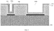
- the retained portion of the protective layer 118 in the first cavity 108 a is removed.
- the removal of the remaining portion of the protective layer 118 is carried out by selective etching as described above and may be performed by a wet etch or a dry etch process controlled by a predetermined time. As shown in FIG. 7 , the removal of the remaining portion of the protective layer 118 exposes the underlying first material layer 116 within the first cavity 108 a.
- a second material layer 124 is formed in the first and second cavities ( 108 a and 108 b , respectively).
- the second material layer 124 may be formed by conventional deposition processes; however, a highly conformal process (e.g., ALD process or highly-controlled CVD process) is preferred.
- the second material layer 124 is deposited over the entire top surface of the set of device features in FIG. 7 , including the first and second cavities ( 108 a and 108 b , respectively).
- the second material layer 124 may be formed by conventional deposition processes; however, a highly conformal process (e.g., ALD process or highly-controlled CVD process) is preferred.
- the second material layer 124 is formed on the portion of the dielectric layer 114 that overlies the dielectric structure 106 , and is also formed on the retained first material layer 116 in the first cavity 108 a.
- the second material layer 124 is a second WFM layer and may include any metallic compound or a composition of metallic compounds capable of modifying the work function property of a gate electrode, as described in FIG. 3 .
- the second WFM layer 124 may have the same or different compound as the first WFM layer 116 .
- the second WFM layer 124 may have the same or different thickness as the first WFM layer 116 .
- the second WFM layer 124 may have a thickness in the range of about 0.5 nm to about 10 nm.
- the second WFM layer 124 is a titanium nitride layer.
- a sacrificial block layer 126 is formed to cover the protective layer 118 , including within the second cavity 108 b .
- the sacrificial block layer 126 may be formed by a conventional deposition process, such as spin-on coating or CVD.
- the sacrificial block layer 126 is a spin-on carbon material.
- the spin-on carbon material may include a polymeric compound containing atoms selected from the group consisting of carbon, hydrogen, oxygen, and nitrogen.
- the sacrificial block layer 126 is subsequently removed by a planarization process (e.g., chemical mechanical planarization (CMP)) or a selective etching process such that the sacrificial block layer 126 is retained only in the second cavity 108 b .
- a planarization process e.g., chemical mechanical planarization (CMP)
- CMP chemical mechanical planarization
- a selective etching process such that the sacrificial block layer 126 is retained only in the second cavity 108 b .
- the protective layer 118 within the first cavity 108 a has a thickness w 2
- the protective layer 118 within the second cavity 108 b has a thickness w 1 .
- a first isotropic etch is performed on the protective layer 118 to selectively remove the protective layer 118 from the first cavity 108 a and retain the protective layer 118 in the second cavity 108 b .
- the first isotropic etching may be a wet etch process or a dry etch process, and may be controlled by a predetermined time.
- the removal of the protective layer 118 from the first cavity 108 a exposes the underlying first material layer 116 , while the protective layer 118 retained in the second cavity 108 b is etched below the top surface 132 of the dielectric structure 106 .
- the vertical etch rate of the protective layer 118 in the first cavity 108 a is faster than the vertical etch rate of the protective layer 118 in the second cavity 108 b . Accordingly, the retained portion of the protective layer 118 in the second cavity 108 b has top edges 130 that are formed simultaneously with the removal of the portion of the protective layer 118 from the first cavity 108 a . In this embodiment, the top edges 130 are etched below the top surface 132 of the dielectric structure 106 .
- the presence of the sacrificial block layer 126 in the second cavity 108 b ensures that only portions of the protective layer 118 deposited over the sidewall surfaces 120 b of the second cavity 108 b are removed during the first isotropic etch.
- the sacrificial block layer 126 is selectively and completely removed from the second cavity 108 b and exposes the protective layer 118 .
- the sacrificial block layer 126 may be removed using an isotropic etching process (e.g., a wet etch).
- a second isotropic etch is performed on the first material layer 116 to selectively remove first material layer 116 from the first cavity 108 a and retain a portion of the first material layer 116 in the second cavity 108 b .
- the second isotropic etching may be a wet etch process or a dry etch process, and may be controlled by a predetermined time.
- the removal of the first material layer 116 from the first cavity 108 a exposes the underlying dielectric layer 114 .
- the retained portion of the first material layer 116 in the second cavity 108 b has top edges 134 that are formed simultaneously with the removal of the portion of the protective layer 118 from the first cavity 108 a .
- the first material layer 116 extends over only a portion of the dielectric layer 114 on the sidewall surfaces 120 b of the second cavity 108 b . Additionally, the top edges 134 of the first material layer 116 are etched below the top surface 132 of the dielectric structure 106 .
- the retained portion of the protective layer 118 in the second cavity 108 b is removed, in the same manner described in FIG. 7 .
- the removal of the retained portion of the protective layer 118 exposes the underlying first material layer 116 within the second cavity 108 b.
- a second material layer 124 is deposited over the surface of the device structure, including the first and second cavities ( 108 a and 108 b , respectively).
- the second material layer 124 may be formed by conventional deposition processes; however, a highly conformal process (e.g., ALD process or highly-controlled CVD process) is preferred.
- the second material layer 124 conformally covers the top edges 134 of the first material layer 116 creating a step on each side of the second cavity 108 b.
- the protective layer 118 provides etch protection for the covered portion of the first material layer 116 in the first cavity 108 a while allowing the uncovered portion of the first material layer 116 in the second cavity 108 b to be removed, and vice versa.
- the presence of the protective layer 118 is found to enable selective retention of the first material layer 116 in either the first cavity 108 a or the second cavity 108 b after the second isotropic etch.
- the present method does not use additional photolithography mask to enable partial removal of the protective layer 118 and the first material layer 116 described herein.
- the first and second material layers ( 116 and 124 , respectively) are first and second WFM layers, respectively, and constitutes the work-function component of a gate electrode.
- the first and second WFM layers ( 116 and 124 , respectively) may be of the same or different material compositions, and may also have the same or different thicknesses with respect to each other.
- the work function component in the first gate cavity 108 a includes both first and second WFM layers ( 116 and 124 , respectively) while the work function component in the second gate cavity 108 b includes only the second WFM layer 124 .
- the first and second WFM layers ( 116 and 124 , respectively) in the first gate cavity 108 a are formed using the same compound.
- the work function component in the first gate cavity 108 a is modified to be thicker than the work function component in the second gate cavity 108 b . Accordingly, the threshold voltage of the first gate cavity 108 a is found to be lower than the threshold voltage of the second gate cavity 108 b.
- the first and second WFM layers ( 116 and 124 , respectively) in the first gate cavity 108 a are formed using different compounds, while the second cavity 108 b includes only the second WFM layer 124 . Accordingly, the threshold voltage of the first gate cavity 108 a is found to be lower than the threshold voltage of the second gate cavity 108 b.
- the present method is found to enable the fabrication of multiple gate electrodes having dissimilar thicknesses/material compositions of the work function component without having to use a photolithography mask (e.g., a reticle mask), thereby significantly reducing the fabrication cost of the semiconductor device. More advantageously, the present method is found to enable the formation of multiple gate electrodes having different threshold voltage properties in the semiconductor device.
- a photolithography mask e.g., a reticle mask
- top, upper, upwards, over, and above refer to the direction away from the active region.
- bottom, lower, downwards, under, and below refer to the direction towards the active region. It is to be understood that the terms so used are interchangeable under appropriate circumstances such that the embodiments of the device described herein are, for example, capable of operation in other orientations than those illustrated or otherwise described herein.
- the methods of forming the semiconductor structure disclosed herein may be employed in replacement metal gate processes for forming gate electrode components on a semiconductor device, and may be employed in manufacturing a variety of different integrated circuit products, including, but not limited to, logic products, memory products, 3D transistor devices, FinFET transistor devices, planar transistor devices, CMOS devices, SOI devices etc.
Landscapes
- Chemical & Material Sciences (AREA)
- Crystallography & Structural Chemistry (AREA)
- Chemical Kinetics & Catalysis (AREA)
- General Chemical & Material Sciences (AREA)
- Physics & Mathematics (AREA)
- Engineering & Computer Science (AREA)
- Plasma & Fusion (AREA)
- Insulated Gate Type Field-Effect Transistor (AREA)
- Metal-Oxide And Bipolar Metal-Oxide Semiconductor Integrated Circuits (AREA)
Abstract
Description
Claims (19)
Priority Applications (1)
| Application Number | Priority Date | Filing Date | Title |
|---|---|---|---|
| US16/396,775 US10896853B2 (en) | 2019-04-29 | 2019-04-29 | Mask-free methods of forming structures in a semiconductor device |
Applications Claiming Priority (1)
| Application Number | Priority Date | Filing Date | Title |
|---|---|---|---|
| US16/396,775 US10896853B2 (en) | 2019-04-29 | 2019-04-29 | Mask-free methods of forming structures in a semiconductor device |
Publications (2)
| Publication Number | Publication Date |
|---|---|
| US20200343142A1 US20200343142A1 (en) | 2020-10-29 |
| US10896853B2 true US10896853B2 (en) | 2021-01-19 |
Family
ID=72916591
Family Applications (1)
| Application Number | Title | Priority Date | Filing Date |
|---|---|---|---|
| US16/396,775 Active US10896853B2 (en) | 2019-04-29 | 2019-04-29 | Mask-free methods of forming structures in a semiconductor device |
Country Status (1)
| Country | Link |
|---|---|
| US (1) | US10896853B2 (en) |
Citations (4)
| Publication number | Priority date | Publication date | Assignee | Title |
|---|---|---|---|---|
| US6586808B1 (en) | 2002-06-06 | 2003-07-01 | Advanced Micro Devices, Inc. | Semiconductor device having multi-work function gate electrode and multi-segment gate dielectric |
| US6794234B2 (en) | 2002-01-30 | 2004-09-21 | The Regents Of The University Of California | Dual work function CMOS gate technology based on metal interdiffusion |
| US7229873B2 (en) | 2005-08-10 | 2007-06-12 | Texas Instruments Incorporated | Process for manufacturing dual work function metal gates in a microelectronics device |
| US20130187236A1 (en) * | 2012-01-20 | 2013-07-25 | Globalfoundries Inc. | Methods of Forming Replacement Gate Structures for Semiconductor Devices |
-
2019
- 2019-04-29 US US16/396,775 patent/US10896853B2/en active Active
Patent Citations (4)
| Publication number | Priority date | Publication date | Assignee | Title |
|---|---|---|---|---|
| US6794234B2 (en) | 2002-01-30 | 2004-09-21 | The Regents Of The University Of California | Dual work function CMOS gate technology based on metal interdiffusion |
| US6586808B1 (en) | 2002-06-06 | 2003-07-01 | Advanced Micro Devices, Inc. | Semiconductor device having multi-work function gate electrode and multi-segment gate dielectric |
| US7229873B2 (en) | 2005-08-10 | 2007-06-12 | Texas Instruments Incorporated | Process for manufacturing dual work function metal gates in a microelectronics device |
| US20130187236A1 (en) * | 2012-01-20 | 2013-07-25 | Globalfoundries Inc. | Methods of Forming Replacement Gate Structures for Semiconductor Devices |
Also Published As
| Publication number | Publication date |
|---|---|
| US20200343142A1 (en) | 2020-10-29 |
Similar Documents
| Publication | Publication Date | Title |
|---|---|---|
| US11177258B2 (en) | Stacked nanosheet CFET with gate all around structure | |
| US10985064B2 (en) | Buried power and ground in stacked vertical transport field effect transistors | |
| US10367069B2 (en) | Fabrication of vertical field effect transistor structure with controlled gate length | |
| US10297513B1 (en) | Stacked vertical NFET and PFET | |
| US7538000B2 (en) | Method of forming double gate transistors having varying gate dielectric thicknesses | |
| US12087637B2 (en) | Semiconductor device and method of manufacture | |
| US11315922B2 (en) | Fin cut to prevent replacement gate collapse on STI | |
| US11094827B2 (en) | Semiconductor devices with uniform gate height and method of forming same | |
| US11031389B2 (en) | Semiconductor structures over active region and methods of forming the structures | |
| US10937685B2 (en) | Diffusion break structures in semiconductor devices | |
| JP2024542366A (en) | Fork and seat with reduced coupling effect | |
| US20240363424A1 (en) | Semiconductor device and method of manufacture | |
| US20250185344A1 (en) | Semiconductor Device and Method of Manufacture | |
| US20200066600A1 (en) | Reducing Off-State Leakage Current in Si/SiGe Dual Channel CMOS | |
| CN112420515A (en) | Method of forming semiconductor device | |
| US8202780B2 (en) | Method for manufacturing a FinFET device comprising a mask to define a gate perimeter and another mask to define fin regions | |
| US10896853B2 (en) | Mask-free methods of forming structures in a semiconductor device | |
| US7435646B2 (en) | Method for forming floating gates within NVM process | |
| US11004953B2 (en) | Mask-free methods of forming structures in a semiconductor device | |
| US10388570B2 (en) | Substrate with a fin region comprising a stepped height structure | |
| TWI859921B (en) | Semiconductor device and manufacturing method thereof | |
| US11302794B2 (en) | FinFET with dual work function metal | |
| US20240429281A1 (en) | Metal gates for semiconductor devices and method thereof |
Legal Events
| Date | Code | Title | Description |
|---|---|---|---|
| AS | Assignment |
Owner name: GLOBALFOUNDRIES INC., CAYMAN ISLANDS Free format text: ASSIGNMENT OF ASSIGNORS INTEREST;ASSIGNORS:SHU, JIEHUI;LEE, RINUS TEK PO;HONG, WEI;AND OTHERS;SIGNING DATES FROM 20190417 TO 20190426;REEL/FRAME:049015/0813 |
|
| FEPP | Fee payment procedure |
Free format text: ENTITY STATUS SET TO UNDISCOUNTED (ORIGINAL EVENT CODE: BIG.); ENTITY STATUS OF PATENT OWNER: LARGE ENTITY |
|
| AS | Assignment |
Owner name: GLOBALFOUNDRIES U.S. INC., CALIFORNIA Free format text: ASSIGNMENT OF ASSIGNORS INTEREST;ASSIGNOR:GLOBALFOUNDRIES INC.;REEL/FRAME:054633/0001 Effective date: 20201022 |
|
| STPP | Information on status: patent application and granting procedure in general |
Free format text: PUBLICATIONS -- ISSUE FEE PAYMENT VERIFIED |
|
| STCF | Information on status: patent grant |
Free format text: PATENTED CASE |
|
| AS | Assignment |
Owner name: GLOBALFOUNDRIES U.S. INC., NEW YORK Free format text: RELEASE BY SECURED PARTY;ASSIGNOR:WILMINGTON TRUST, NATIONAL ASSOCIATION;REEL/FRAME:056987/0001 Effective date: 20201117 Owner name: GLOBALFOUNDRIES U.S. INC., NEW YORK Free format text: RELEASE OF SECURITY INTEREST;ASSIGNOR:WILMINGTON TRUST, NATIONAL ASSOCIATION;REEL/FRAME:056987/0001 Effective date: 20201117 |
|
| MAFP | Maintenance fee payment |
Free format text: PAYMENT OF MAINTENANCE FEE, 4TH YEAR, LARGE ENTITY (ORIGINAL EVENT CODE: M1551); ENTITY STATUS OF PATENT OWNER: LARGE ENTITY Year of fee payment: 4 |