US10879134B2 - Techniques for monolithic co-integration of silicon and III-N semiconductor transistors - Google Patents
Techniques for monolithic co-integration of silicon and III-N semiconductor transistors Download PDFInfo
- Publication number
- US10879134B2 US10879134B2 US16/302,414 US201616302414A US10879134B2 US 10879134 B2 US10879134 B2 US 10879134B2 US 201616302414 A US201616302414 A US 201616302414A US 10879134 B2 US10879134 B2 US 10879134B2
- Authority
- US
- United States
- Prior art keywords
- layer
- semiconductor layer
- semiconductor
- iii
- silicon
- Prior art date
- Legal status (The legal status is an assumption and is not a legal conclusion. Google has not performed a legal analysis and makes no representation as to the accuracy of the status listed.)
- Expired - Fee Related
Links
Images


Classifications
-
- H01L21/8258—
-
- H01L21/02381—
-
- H01L21/02532—
-
- H01L21/0254—
-
- H01L21/02609—
-
- H01L27/0605—
-
- H01L27/092—
-
- H01L27/1207—
-
- H01L29/045—
-
- H01L29/0847—
-
- H01L29/16—
-
- H01L29/2003—
-
- H—ELECTRICITY
- H10—SEMICONDUCTOR DEVICES; ELECTRIC SOLID-STATE DEVICES NOT OTHERWISE PROVIDED FOR
- H10D—INORGANIC ELECTRIC SEMICONDUCTOR DEVICES
- H10D62/00—Semiconductor bodies, or regions thereof, of devices having potential barriers
- H10D62/10—Shapes, relative sizes or dispositions of the regions of the semiconductor bodies; Shapes of the semiconductor bodies
- H10D62/13—Semiconductor regions connected to electrodes carrying current to be rectified, amplified or switched, e.g. source or drain regions
- H10D62/149—Source or drain regions of field-effect devices
- H10D62/151—Source or drain regions of field-effect devices of IGFETs
-
- H—ELECTRICITY
- H10—SEMICONDUCTOR DEVICES; ELECTRIC SOLID-STATE DEVICES NOT OTHERWISE PROVIDED FOR
- H10D—INORGANIC ELECTRIC SEMICONDUCTOR DEVICES
- H10D62/00—Semiconductor bodies, or regions thereof, of devices having potential barriers
- H10D62/40—Crystalline structures
- H10D62/405—Orientations of crystalline planes
-
- H—ELECTRICITY
- H10—SEMICONDUCTOR DEVICES; ELECTRIC SOLID-STATE DEVICES NOT OTHERWISE PROVIDED FOR
- H10D—INORGANIC ELECTRIC SEMICONDUCTOR DEVICES
- H10D62/00—Semiconductor bodies, or regions thereof, of devices having potential barriers
- H10D62/80—Semiconductor bodies, or regions thereof, of devices having potential barriers characterised by the materials
- H10D62/83—Semiconductor bodies, or regions thereof, of devices having potential barriers characterised by the materials being Group IV materials, e.g. B-doped Si or undoped Ge
-
- H—ELECTRICITY
- H10—SEMICONDUCTOR DEVICES; ELECTRIC SOLID-STATE DEVICES NOT OTHERWISE PROVIDED FOR
- H10D—INORGANIC ELECTRIC SEMICONDUCTOR DEVICES
- H10D62/00—Semiconductor bodies, or regions thereof, of devices having potential barriers
- H10D62/80—Semiconductor bodies, or regions thereof, of devices having potential barriers characterised by the materials
- H10D62/85—Semiconductor bodies, or regions thereof, of devices having potential barriers characterised by the materials being Group III-V materials, e.g. GaAs
- H10D62/8503—Nitride Group III-V materials, e.g. AlN or GaN
-
- H—ELECTRICITY
- H10—SEMICONDUCTOR DEVICES; ELECTRIC SOLID-STATE DEVICES NOT OTHERWISE PROVIDED FOR
- H10D—INORGANIC ELECTRIC SEMICONDUCTOR DEVICES
- H10D84/00—Integrated devices formed in or on semiconductor substrates that comprise only semiconducting layers, e.g. on Si wafers or on GaAs-on-Si wafers
- H10D84/01—Manufacture or treatment
- H10D84/02—Manufacture or treatment characterised by using material-based technologies
- H10D84/08—Manufacture or treatment characterised by using material-based technologies using combinations of technologies, e.g. using both Si and SiC technologies or using both Si and Group III-V technologies
-
- H—ELECTRICITY
- H10—SEMICONDUCTOR DEVICES; ELECTRIC SOLID-STATE DEVICES NOT OTHERWISE PROVIDED FOR
- H10D—INORGANIC ELECTRIC SEMICONDUCTOR DEVICES
- H10D84/00—Integrated devices formed in or on semiconductor substrates that comprise only semiconducting layers, e.g. on Si wafers or on GaAs-on-Si wafers
- H10D84/80—Integrated devices formed in or on semiconductor substrates that comprise only semiconducting layers, e.g. on Si wafers or on GaAs-on-Si wafers characterised by the integration of at least one component covered by groups H10D12/00 or H10D30/00, e.g. integration of IGFETs
- H10D84/82—Integrated devices formed in or on semiconductor substrates that comprise only semiconducting layers, e.g. on Si wafers or on GaAs-on-Si wafers characterised by the integration of at least one component covered by groups H10D12/00 or H10D30/00, e.g. integration of IGFETs of only field-effect components
- H10D84/83—Integrated devices formed in or on semiconductor substrates that comprise only semiconducting layers, e.g. on Si wafers or on GaAs-on-Si wafers characterised by the integration of at least one component covered by groups H10D12/00 or H10D30/00, e.g. integration of IGFETs of only field-effect components of only insulated-gate FETs [IGFET]
- H10D84/85—Complementary IGFETs, e.g. CMOS
-
- H—ELECTRICITY
- H10—SEMICONDUCTOR DEVICES; ELECTRIC SOLID-STATE DEVICES NOT OTHERWISE PROVIDED FOR
- H10D—INORGANIC ELECTRIC SEMICONDUCTOR DEVICES
- H10D87/00—Integrated devices comprising both bulk components and either SOI or SOS components on the same substrate
-
- H—ELECTRICITY
- H10—SEMICONDUCTOR DEVICES; ELECTRIC SOLID-STATE DEVICES NOT OTHERWISE PROVIDED FOR
- H10P—GENERIC PROCESSES OR APPARATUS FOR THE MANUFACTURE OR TREATMENT OF DEVICES COVERED BY CLASS H10
- H10P14/00—Formation of materials, e.g. in the shape of layers or pillars
- H10P14/20—Formation of materials, e.g. in the shape of layers or pillars of semiconductor materials
- H10P14/29—Formation of materials, e.g. in the shape of layers or pillars of semiconductor materials characterised by the substrates
- H10P14/2901—Materials
- H10P14/2902—Materials being Group IVA materials
- H10P14/2905—Silicon, silicon germanium or germanium
-
- H—ELECTRICITY
- H10—SEMICONDUCTOR DEVICES; ELECTRIC SOLID-STATE DEVICES NOT OTHERWISE PROVIDED FOR
- H10P—GENERIC PROCESSES OR APPARATUS FOR THE MANUFACTURE OR TREATMENT OF DEVICES COVERED BY CLASS H10
- H10P14/00—Formation of materials, e.g. in the shape of layers or pillars
- H10P14/20—Formation of materials, e.g. in the shape of layers or pillars of semiconductor materials
- H10P14/34—Deposited materials, e.g. layers
- H10P14/3402—Deposited materials, e.g. layers characterised by the chemical composition
- H10P14/3404—Deposited materials, e.g. layers characterised by the chemical composition being Group IVA materials
- H10P14/3411—Silicon, silicon germanium or germanium
-
- H—ELECTRICITY
- H10—SEMICONDUCTOR DEVICES; ELECTRIC SOLID-STATE DEVICES NOT OTHERWISE PROVIDED FOR
- H10P—GENERIC PROCESSES OR APPARATUS FOR THE MANUFACTURE OR TREATMENT OF DEVICES COVERED BY CLASS H10
- H10P14/00—Formation of materials, e.g. in the shape of layers or pillars
- H10P14/20—Formation of materials, e.g. in the shape of layers or pillars of semiconductor materials
- H10P14/34—Deposited materials, e.g. layers
- H10P14/3402—Deposited materials, e.g. layers characterised by the chemical composition
- H10P14/3414—Deposited materials, e.g. layers characterised by the chemical composition being group IIIA-VIA materials
- H10P14/3416—Nitrides
-
- H—ELECTRICITY
- H10—SEMICONDUCTOR DEVICES; ELECTRIC SOLID-STATE DEVICES NOT OTHERWISE PROVIDED FOR
- H10P—GENERIC PROCESSES OR APPARATUS FOR THE MANUFACTURE OR TREATMENT OF DEVICES COVERED BY CLASS H10
- H10P14/00—Formation of materials, e.g. in the shape of layers or pillars
- H10P14/20—Formation of materials, e.g. in the shape of layers or pillars of semiconductor materials
- H10P14/34—Deposited materials, e.g. layers
- H10P14/3466—Crystal orientation
-
- H01L21/76254—
-
- H01L21/823807—
-
- H01L29/66522—
-
- H01L29/66545—
-
- H01L29/66568—
-
- H01L29/66628—
-
- H—ELECTRICITY
- H10—SEMICONDUCTOR DEVICES; ELECTRIC SOLID-STATE DEVICES NOT OTHERWISE PROVIDED FOR
- H10D—INORGANIC ELECTRIC SEMICONDUCTOR DEVICES
- H10D30/00—Field-effect transistors [FET]
- H10D30/01—Manufacture or treatment
- H10D30/021—Manufacture or treatment of FETs having insulated gates [IGFET]
- H10D30/027—Manufacture or treatment of FETs having insulated gates [IGFET] of lateral single-gate IGFETs
- H10D30/0275—Manufacture or treatment of FETs having insulated gates [IGFET] of lateral single-gate IGFETs forming single crystalline semiconductor source or drain regions resulting in recessed gates, e.g. forming raised source or drain regions
-
- H—ELECTRICITY
- H10—SEMICONDUCTOR DEVICES; ELECTRIC SOLID-STATE DEVICES NOT OTHERWISE PROVIDED FOR
- H10D—INORGANIC ELECTRIC SEMICONDUCTOR DEVICES
- H10D64/00—Electrodes of devices having potential barriers
- H10D64/01—Manufacture or treatment
- H10D64/017—Manufacture or treatment using dummy gates in processes wherein at least parts of the final gates are self-aligned to the dummy gates, i.e. replacement gate processes
-
- H—ELECTRICITY
- H10—SEMICONDUCTOR DEVICES; ELECTRIC SOLID-STATE DEVICES NOT OTHERWISE PROVIDED FOR
- H10D—INORGANIC ELECTRIC SEMICONDUCTOR DEVICES
- H10D84/00—Integrated devices formed in or on semiconductor substrates that comprise only semiconducting layers, e.g. on Si wafers or on GaAs-on-Si wafers
- H10D84/01—Manufacture or treatment
- H10D84/0123—Integrating together multiple components covered by H10D12/00 or H10D30/00, e.g. integrating multiple IGBTs
- H10D84/0126—Integrating together multiple components covered by H10D12/00 or H10D30/00, e.g. integrating multiple IGBTs the components including insulated gates, e.g. IGFETs
- H10D84/0165—Integrating together multiple components covered by H10D12/00 or H10D30/00, e.g. integrating multiple IGBTs the components including insulated gates, e.g. IGFETs the components including complementary IGFETs, e.g. CMOS devices
- H10D84/0167—Manufacturing their channels
-
- H—ELECTRICITY
- H10—SEMICONDUCTOR DEVICES; ELECTRIC SOLID-STATE DEVICES NOT OTHERWISE PROVIDED FOR
- H10D—INORGANIC ELECTRIC SEMICONDUCTOR DEVICES
- H10D84/00—Integrated devices formed in or on semiconductor substrates that comprise only semiconducting layers, e.g. on Si wafers or on GaAs-on-Si wafers
- H10D84/01—Manufacture or treatment
- H10D84/02—Manufacture or treatment characterised by using material-based technologies
- H10D84/03—Manufacture or treatment characterised by using material-based technologies using Group IV technology, e.g. silicon technology or silicon-carbide [SiC] technology
- H10D84/038—Manufacture or treatment characterised by using material-based technologies using Group IV technology, e.g. silicon technology or silicon-carbide [SiC] technology using silicon technology, e.g. SiGe
-
- H—ELECTRICITY
- H10—SEMICONDUCTOR DEVICES; ELECTRIC SOLID-STATE DEVICES NOT OTHERWISE PROVIDED FOR
- H10P—GENERIC PROCESSES OR APPARATUS FOR THE MANUFACTURE OR TREATMENT OF DEVICES COVERED BY CLASS H10
- H10P90/00—Preparation of wafers not covered by a single main group of this subclass, e.g. wafer reinforcement
- H10P90/19—Preparing inhomogeneous wafers
- H10P90/1904—Preparing vertically inhomogeneous wafers
- H10P90/1906—Preparing SOI wafers
- H10P90/1914—Preparing SOI wafers using bonding
- H10P90/1916—Preparing SOI wafers using bonding with separation or delamination along an ion implanted layer, e.g. Smart-cut
-
- H—ELECTRICITY
- H10—SEMICONDUCTOR DEVICES; ELECTRIC SOLID-STATE DEVICES NOT OTHERWISE PROVIDED FOR
- H10W—GENERIC PACKAGES, INTERCONNECTIONS, CONNECTORS OR OTHER CONSTRUCTIONAL DETAILS OF DEVICES COVERED BY CLASS H10
- H10W10/00—Isolation regions in semiconductor bodies between components of integrated devices
- H10W10/10—Isolation regions comprising dielectric materials
- H10W10/181—Semiconductor-on-insulator [SOI] isolation regions, e.g. buried oxide regions of SOI wafers
Definitions
- a field-effect transistor is a semiconductor device that includes three terminals: a gate, a source, and a drain. Through application of an electric field produced by the gate, the electrical conductivity of a nearby semiconductor channel may be controlled in a manner that allows charge carriers, such as electrons or holes, to flow between the source and drain. In instances where the charge carriers are electrons, the FET is referred to as an n-channel device. In instances where the charge carriers are holes, the FET is referred to as a p-channel device. Some FETs have a fourth terminal known as the body or substrate, which can be used to bias the transistor.
- MOSFET metal-oxide-semiconductor FET
- CMOS Complementary MOS
- PMOS p-channel MOS
- NMOS n-channel MOS
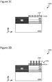
- FIGS. 1A-1F illustrate a process flow for forming an integrated circuit (IC) in accordance with an embodiment of the present disclosure.
- FIGS. 2A-2F illustrate a process flow for forming an IC in accordance with another embodiment of the present disclosure.
- FIG. 3 illustrates a computing system implemented with integrated circuit structures or devices formed using the disclosed techniques in accordance with an example embodiment.
- the disclosed techniques may be used to provide a silicon-on-insulator (SOI) or other semiconductor-on-insulator structure including: (1) a Si (111) surface available for formation of III-N-based n-channel devices; and (2) a Si (100) surface available for formation of Si-based p-channel devices, n-channel devices, or both. Further processing may be performed, in accordance with some embodiments, to provide n-channel and p-channel devices over the Si (111) and Si (100) surfaces, as desired.
- SOI silicon-on-insulator
- the disclosed techniques may be used to provide co-integrated III-N-based n-type metal-oxide-semiconductor (NMOS) devices and Si-based p-type metal-oxide-semiconductor (PMOS), NMOS, or complementary MOS (CMOS) devices with different step heights or with a given degree of co-planarity, as desired for a given target application or end-use.
- NMOS n-type metal-oxide-semiconductor
- PMOS p-type metal-oxide-semiconductor
- CMOS complementary MOS
- Gallium nitride has a very high bandgap and simultaneously high mobility and is thus suitable for n-channel transistor devices typically implemented in voltage regulators (VRs) and other power management integrated circuits (PMICs), as well as RF power amplifiers (PAs).
- VRs voltage regulators
- PMICs power management integrated circuits
- PAs RF power amplifiers
- GaN is not particularly adequate for use in the p-channel transistor devices of such logic and controller circuitry.
- the p-channel can be implemented with an alternative material such as silicon (Si), processing difficulties may arise because GaN growth normally employs a Si (111) surface orientation (rather than a Si (100) surface orientation) and there may be a significant step height difference between relatively thick GaN layers and the underlying Si substrate.
- Si silicon
- the disclosed techniques may be used to provide a SOI or other semiconductor-on-insulator structure including: (1) a Si (111) surface over which III-N-based n-channel devices may be formed; and (2) a Si (100) surface over which Si-based p-channel devices, n-channel devices, or both, may be formed. Further processing may be performed, in accordance with some embodiments, to provide such n-channel and p-channel devices over the available Si (111) and Si (100) surfaces.
- the disclosed techniques may be used to provide III-N-based NMOS devices and Si-based PMOS, NMOS, or complementary MOS (CMOS) devices with different step heights or with a given degree of co-planarity, as desired for a given target application or end-use.
- CMOS complementary MOS
- a lightly p-doped (p) epitaxial Si (100) layer may be formed over a Si (100) substrate. Then, a buried oxide (BOX) layer may be formed over the p ⁇ epitaxial Si (100) layer, and a Si (111) layer may be transferred to the BOX layer from a carrier substrate. Thereafter, in some cases, a III-N semiconductor layer may be formed over the Si (111) layer (optionally with an intervening nucleation layer), and then the Si (111) layer and BOX layer may be partially removed so as to expose a first portion of the p ⁇ epitaxial Si (100) layer.
- a buried oxide (BOX) layer may be formed over the p ⁇ epitaxial Si (100) layer, and a Si (111) layer may be transferred to the BOX layer from a carrier substrate.
- a III-N semiconductor layer may be formed over the Si (111) layer (optionally with an intervening nucleation layer), and then the Si (111) layer and BOX
- the Si (111) layer and BOX layer may be partially removed so as to expose the first portion of the p ⁇ epitaxial Si (100) layer, and then the III-N semiconductor layer may be formed over the Si (111) layer (optionally with an intervening nucleation layer). In either instance, the III-N semiconductor layer may be disposed over a second portion of the p ⁇ epitaxial Si (100) layer that is different from the first portion.
- Si p-channel or n-channel device(s) may be formed over the first portion of the p ⁇ epitaxial Si (100) layer, and III-N semiconductor device(s) may be formed over the III-N semiconductor layer disposed over the second portion of the p ⁇ epitaxial Si (100) layer.
- a BOX layer may be formed over a Si (111) substrate. Then, a Si (100) layer and a p ⁇ epitaxial Si (100) layer may be transferred to the BOX layer from a carrier substrate. Then, the Si (100) layer and BOX layer may be partially removed so as to expose a first portion of the Si (111) substrate, and a III-N semiconductor layer may be formed over that first portion (optionally with an intervening nucleation layer).
- Si p-channel or n-channel device(s) may be formed over the Si (100) layer so as to be disposed over a second portion of the Si (111) substrate that is different from the first portion, and III-N semiconductor device(s) may be formed over the III-N semiconductor layer disposed over the first portion of the Si (111) substrate.
- the different crystallographic surface orientations made available by a given structure provided as described herein may be configured to cater to both high-performance, high-voltage GaN (or other III-N) NMOS and Si PMOS, NMOS, or CMOS devices.
- co-integration of complete PMIC or RF frontend circuits that include both p-channel and n-channel devices may be permitted to proceed on separate portions of a Si wafer or other semiconductor substrate.
- a first area of a semiconductor substrate may be designated for a Si p-channel device, whereas a second, different area of the semiconductor substrate may be designated for a GaN or other III-N n-channel device, in accordance with some embodiments.
- the Si device area and the III-N device area may be at different step heights (e.g., depending on which initial SOI or other semiconductor-on-insulator structure is implemented), as well as on the thicknesses of different constituent layers, such as the III-N semiconductor layer(s) and BOX layer(s), among others.
- a co-integration scheme provided via the techniques disclosed herein may account for the thermal budget of each layer present, allowing III-N processing (e.g., which may involve formation temperatures in excess of 1,000° C.) to proceed before Si processing.
- the disclosed techniques may be used, for example, to provide monolithic co-integration of Si PMOS (or NMOS or CMOS) and III-N-based NMOS over different crystal planes of a SOI or other semiconductor-on-insulator structure.
- the disclosed techniques may be used, for example, in providing high-performance VR circuits, RF frontend devices, and other system-on-chip (SoC) products in GaN that are monolithically co-integrated with Si or any other PMOS.
- SoC system-on-chip
- the disclosed techniques may be used, for example, in providing SOI or other semiconductor-on-insulator structures which provide opportunities for substrate choice and layer formation based, at least in part, on operation requirements or other target performance parameters of RF and PMIC devices to be formed. For instance, it may be desirable to maximize or otherwise provide high resistivity (e.g., on the order of about 1 k ⁇ cm) for GaN-based RF devices, whereas it may be desirable to minimize or otherwise provide low resistivity (e.g., on the order of about 10 ⁇ cm) to allow for tuning of doping schemes for logic devices. To these ends, the disclosed techniques may be used, for example, in a manner allowing for optimizing or otherwise customizing resistivity for a given target application or end-use, in accordance with some embodiments.
- high resistivity e.g., on the order of about 1 k ⁇ cm
- low resistivity e.g., on the order of about 10 ⁇ cm
- the disclosed techniques may involve transferring one or more semiconductor layers from a carrier substrate to a layer stack disposed over a semiconductor substrate, in accordance with some embodiments. As will be appreciated in light of this disclosure, this provides an opportunity for intentionally varying the alignment of the alignment notch of the carrier substrate with respect to the alignment notch of the semiconductor substrate. In accordance with some embodiments, intentionally placing the semiconductor substrate and a given overlying semiconductor layer in different notch alignment may allow for customizing device performance and epitaxial layer growth capabilities. For example, use of the disclosed techniques may provide opportunities for Si (100) and Si (111) to be notch-aligned in a given manner to provide optimal (or other desired) transport for Si PMOS (or NMOS or CMOS) and III-N NMOS formation.
- use of the disclosed techniques may be detected, for example, by any one, or combination, of scanning electron microscopy (SEM), transmission electron microscopy (TEM), chemical composition analysis, energy-dispersive X-ray (EDX) spectroscopy, and secondary ion mass spectrometry (SIMS) of a given IC or other transistor structure having PMOS or NMOS (or both) devices formed over a semiconductor layer of a first crystallographic orientation, which in turn is disposed over a semiconductor substrate of a second, different crystallographic orientation.
- SEM scanning electron microscopy
- TEM transmission electron microscopy
- EDX energy-dispersive X-ray
- SIMS secondary ion mass spectrometry
- FIGS. 1A-1F illustrate a process flow for forming an integrated circuit (IC) 100 a in accordance with an embodiment of the present disclosure.
- this process flow may be used, for example, to fabricate an IC 100 a including a CMOS transistor device 120 a (e.g., Si PMOS, NMOS, or both) and an NMOS transistor device 120 b (e.g., III-N semiconductor NMOS) over a commonly shared semiconductor substrate, in accordance with some embodiments.
- CMOS transistor device 120 a e.g., Si PMOS, NMOS, or both
- NMOS transistor device 120 b e.g., III-N semiconductor NMOS
- the process flow of FIGS. 1A-1F may result in a step height difference between CMOS transistor device 120 a and NMOS transistor device 120 b , as generally can be seen from FIG. 1F .
- IC 100 a may include a semiconductor substrate 102 a , which may have any of a wide range of configurations.
- semiconductor substrate 102 a may be configured as any one, or combination, of a bulk semiconductor substrate, a silicon-on-insulator (SOI) or other semiconductor-on-insulator structure (XOI, where X represents a semiconductor material, such as silicon, germanium, germanium-enriched silicon, and so forth), a semiconductor wafer, and a multi-layered semiconductor structure.
- SOI silicon-on-insulator
- XOI semiconductor-on-insulator structure
- semiconductor substrate 102 a may be comprised of any one, or combination, of semiconductor materials, such as silicon (Si), germanium (Ge), and silicon-germanium (SiGe), among others.
- semiconductor substrate 102 a may be comprised of Si having a crystallographic orientation of (100).
- Other suitable materials and configurations for semiconductor substrate 102 a will depend on a given application and will be apparent in light of this disclosure.
- IC 100 a may include a semiconductor layer 104 disposed over semiconductor substrate 102 a .
- semiconductor layer 104 may be disposed directly on semiconductor substrate 102 a with no layers intervening, whereas in some other cases, one or more intervening layers may be disposed between semiconductor layer 104 and semiconductor substrate 102 a .
- semiconductor layer 104 may be disposed superjacent to semiconductor substrate 102 a , optionally with one or more intervening layers, in accordance with some embodiments.
- semiconductor layer 104 may be comprised of any of the example materials discussed above, for instance, with respect to semiconductor substrate 102 a , in accordance with some embodiments.
- semiconductor layer 104 and semiconductor substrate 102 a may be comprised of the same semiconductor materials (e.g., both semiconductor layer 104 and semiconductor substrate 102 a may be comprised of Si), whereas in some other cases, semiconductor layer 104 and semiconductor substrate 102 a may differ in material composition.
- semiconductor layer 104 may have a crystallographic orientation of (100), though in other embodiments, other crystallographic orientations may be provided.
- semiconductor layer 104 may be of the same crystallographic orientation as semiconductor substrate 102 a , whereas in other instances, semiconductor layer 104 and semiconductor substrate 102 a may be of different crystallographic orientations.
- semiconductor layer 104 may be doped to a conductivity type and dopant concentration desired for a given target application or end-use.
- semiconductor layer 104 may be doped, in accordance with some embodiments, with a p-type dopant, such as boron (B) or gallium (Ga).
- semiconductor layer 104 may be doped so as to have an electrical resistivity in the range of about 5-15 ⁇ cm (e.g., about 5-10 ⁇ cm, about 10-15 ⁇ cm, or any other sub-range in the range of about 5-15 ⁇ cm).
- semiconductor layer 104 may be a lightly p-doped (e.g., p) epitaxial Si layer.
- semiconductor layer 104 may serve to decouple doping of one or more overlying device layers from underlying semiconductor substrate 102 a.
- Semiconductor layer 104 may be formed over semiconductor substrate 102 a via any suitable standard, custom, or proprietary technique(s), as will be apparent in light of this disclosure.
- semiconductor layer 104 may be formed via any one, or combination, of a chemical vapor deposition (CVD) process (e.g., low-pressure CVD, or LPCVD) and a molecular beam epitaxy (MBE) process, among others.
- CVD chemical vapor deposition
- MBE molecular beam epitaxy
- the thickness (e.g., z-thickness in the z-direction) of semiconductor layer 104 may be customized, as desired for a given target application or end-use.
- semiconductor layer 104 may have a z-thickness in the range of about 0.1-2.0 ⁇ m (e.g., about 0.1-0.5 ⁇ m, about 0.5-1.0 ⁇ m, about 1.0-1.5 ⁇ m, about 1.5-2.0 ⁇ m, or any other sub-range in the range of about 0.1-2.0 ⁇ m).
- Other suitable materials, doping schemes, formation techniques, configurations, and dimensions for semiconductor layer 104 will depend on a given application and will be apparent in light of this disclosure.
- IC 100 a may include an insulator layer 106 disposed over semiconductor layer 104 .
- insulator layer 106 may be disposed directly on semiconductor layer 104 with no layers intervening, whereas in some other cases, one or more intervening layers may be disposed between insulator layer 106 and semiconductor layer 104 .
- insulator layer 106 may be disposed superjacent to semiconductor layer 104 , optionally with one or more intervening layers, in accordance with some embodiments.
- Insulator layer 106 may be comprised of any one, or combination, of a wide range of insulator or dielectric materials.
- insulator layer 106 may be formed from an oxide, such as silicon dioxide (SiO 2 ) or carbon-doped oxide (CDO).
- insulator layer 106 may be considered, in a general sense, a buried oxide (BOX) layer.
- insulator layer 106 may be formed from a nitride, such as silicon nitride (Si 3 N 4 ).
- insulator layer 106 may be formed from a carbide, such as silicon carbide (SiC).
- insulator layer 106 may be formed from an oxynitride, such as silicon oxynitride (SiON) or carbon-doped SiON.
- Insulator layer 106 may be formed via any suitable standard, custom, or proprietary technique(s), as will be apparent in light of this disclosure.
- insulator layer 106 may be formed via any one, or combination, of a chemical vapor deposition (CVD) process (e.g., plasma-enhanced CVD, or PECVD) and an atomic layer deposition (ALD) process, among others.
- CVD chemical vapor deposition
- ALD atomic layer deposition
- the thickness (e.g., z-thickness in the z-direction) of insulator layer 106 may be customized, as desired for a given target application or end-use.
- insulator layer 106 may have a z-thickness in the range of about 10 nm-1 ⁇ m (e.g., about 10-250 nm, about 250-500 nm, about 500-750 nm, about 750 nm-1 ⁇ m, or any other sub-range in the range of about 10 nm-1 ⁇ m).
- insulator layer 106 may be desirable, at least in some instances, to provide an insulator layer 106 of sufficient thickness to ensure that it is sufficiently electrically non-leaky for IC 100 a .
- Other suitable materials, formation techniques, configurations, and dimensions for insulator layer 106 will depend on a given application and will be apparent in light of this disclosure.
- IC 100 a may include a semiconductor layer 108 disposed over insulator layer 106 .
- semiconductor layer 108 may be disposed directly on insulator layer 106 with no layers intervening, whereas in some other cases, one or more intervening layers may be disposed between semiconductor layer 108 and insulator layer 106 .
- semiconductor layer 108 may be disposed superjacent to insulator layer 106 , optionally with one or more intervening layers, in accordance with some embodiments.
- semiconductor layer 108 may be comprised of any one, or combination, of the example semiconductor materials discussed above, for instance, with respect to semiconductor substrate 102 a , in accordance with some embodiments.
- semiconductor layer 108 and semiconductor substrate 102 a may be comprised of the same semiconductor materials (e.g., both semiconductor layer 108 and semiconductor substrate 102 a may be comprised of Si), whereas in some other cases, semiconductor layer 108 and semiconductor substrate 102 a may differ in material composition.
- semiconductor layer 108 may have a crystallographic orientation of (111), though in other embodiments, other crystallographic orientations may be provided.
- semiconductor layer 108 and semiconductor substrate 102 a may be of different crystallographic orientation, for example, semiconductor layer 108 may have a crystallographic orientation of (111), and semiconductor substrate 102 a may have a crystallographic orientation of (100).
- Semiconductor layer 108 may be formed via any suitable standard, custom, or proprietary technique(s), as will be apparent in light of this disclosure.
- semiconductor layer 108 may be transferred to IC 100 a from a carrier substrate (e.g., carrier wafer). More particularly, in accordance with an embodiment, semiconductor layer 108 may be initially formed over a carrier substrate and then bonded with insulator layer 106 via any suitable standard, custom, or proprietary bonding technique(s), as will be apparent in light of this disclosure. Thereafter, in accordance with an embodiment, the carrier substrate may be separated from semiconductor layer 108 , leaving behind semiconductor layer 108 as a portion of IC 100 a .
- semiconductor layer 108 may be separated from the carrier substrate via ion cleaving by hydrogen-induced layer exfoliation other suitable exfoliation or layer separation process, as will be apparent in light of this disclosure.
- semiconductor layer 108 before further processing, semiconductor layer 108 optionally may undergo planarization via a chemical-mechanical planarization (CMP) process or other suitable planarization process, as will be apparent in light of this disclosure.
- CMP chemical-mechanical planarization
- the thickness (e.g., z-thickness in the z-direction) of semiconductor layer 108 may be customized, as desired for a given target application or end-use.
- semiconductor layer 108 may have a z-thickness in the range of about 10 nm-100 nm (e.g., about 10-25 nm, about 25-50 nm, about 50-75 nm, about 75 nm-100 nm, or any other sub-range in the range of about 10 nm-100 nm).
- the z-thickness may be adjusted based on the particular amount of strain desired as a result of the ratio between III-N semiconductor layer 110 (discussed below) and underlying semiconductor substrate 102 a .
- Other suitable materials, formation techniques, configurations, and dimensions for semiconductor layer 108 will depend on a given application and will be apparent in light of this disclosure.
- III-N semiconductor layer 110 may be disposed over semiconductor layer 108 .
- III-N semiconductor layer 110 may be disposed directly on semiconductor layer 108 with no layers intervening, whereas in some other cases, one or more intervening layers may be disposed between III-N semiconductor layer 110 and semiconductor layer 108 .
- III-N semiconductor layer 110 may be disposed superjacent to semiconductor layer 108 , optionally with one or more intervening layers, in accordance with some embodiments.
- III-N semiconductor layer 110 may be comprised of any one, or combination, of III-N semiconductor materials, including gallium nitride (GaN), aluminum nitride (AlN), indium nitride (InN), indium gallium nitride (InGaN), aluminum gallium nitride (AlGaN), aluminum indium nitride (AlInN), and aluminum indium gallium nitride (AlInGaN).
- III-N semiconductor materials including gallium nitride (GaN), aluminum nitride (AlN), indium nitride (InN), indium gallium nitride (InGaN), aluminum gallium nitride (AlInGaN).
- III-N semiconductor layer 110 may be formed via any suitable standard, custom, or proprietary technique(s), as will be apparent in light of this disclosure.
- III-N semiconductor layer 110 may be formed via any one, or combination, of a CVD process (e.g., metal-organic chemical vapor deposition, or MOCVD) and an epitaxy process (e.g., metal-organic vapor phase epitaxy, or MOVPE; molecular beam epitaxy, or MBE), among others.
- a CVD process e.g., metal-organic chemical vapor deposition, or MOCVD
- MOVPE metal-organic vapor phase epitaxy
- MBE molecular beam epitaxy
- III-N semiconductor layer 110 may be formed, in part or in whole, via a process involving shallow trench isolation (STI), patterning the STI with feature(s) of sufficient aspect ratio to provide aspect ratio trapping (ART) of defects, filling feature(s) of the patterned STI with III-N material, and performing epitaxial lateral overgrowth (ELO) of the III-N material over a topography of the STI layer.
- STI shallow trench isolation
- III-N semiconductor layer 110 may be formed, in part or in whole, via a process involving a nucleation layer (discussed below).
- III-N semiconductor layer 110 may include one or more three-dimensional semiconductor structures, such as island-like semiconductor bodies or nanowire or nanoribbon semiconductor bodies, to name a few.
- III-N semiconductor layer 110 may be configured as a single-layer structure, whereas in some other embodiments, III-N semiconductor layer 110 may be configured as a bi-layer, tri-layer, or other multi-layer structure.
- III-N semiconductor layer 110 may be configured such that each of a first constituent layer and an immediately adjacent constituent layer (e.g., immediately superjacent and/or immediately subjacent) is comprised of the same III-N semiconductor material.
- III-N semiconductor layer 110 may be configured as a superlattice structure including alternating layers of III-N semiconductor materials.
- III-N semiconductor layer 110 may include a first constituent layer comprised of a first III-N semiconductor material and an immediately adjacent constituent layer (e.g., immediately superjacent and/or immediately subjacent) comprised of a different second III-N semiconductor material.
- the first and second constituent layers may be repeated in an alternating manner or other given desired order. Additional third, fourth, and further constituent layers optionally may be provided, in accordance with some embodiments. Numerous configurations and variations for III-N semiconductor layer 110 will be apparent in light of this disclosure.
- III-N semiconductor layer 110 may be customized, as desired for a given target application or end-use.
- III-N semiconductor layer 110 (or a given constituent layer or body thereof, in cases of a multi-layer or three-dimensional structure) may have a z-thickness in the range of about 1-5 ⁇ m (e.g., about 1-2.5 ⁇ m, about 2.5-5 ⁇ m, or any other sub-range in the range of about 1-5 ⁇ m).
- Other suitable materials, formation techniques, configurations, and dimensions for III-N semiconductor layer 110 will depend on a given application and will be apparent in light of this disclosure.
- a nucleation layer optionally may be formed over semiconductor layer 108 , and III-N semiconductor layer 110 may be formed over that nucleation layer.
- a nucleation layer may be comprised of any one, or combination, of suitable materials, such as aluminum nitride (AlN), aluminum gallium nitride (AlGaN), or an alloy of any thereof, to name a few.
- AlN aluminum nitride
- AlGaN aluminum gallium nitride
- a given optional nucleation layer may be formed via any suitable standard, custom, or proprietary technique(s), as will be apparent in light of this disclosure.
- a given optional nucleation layer may be formed via any one, or combination, of a molecular beam epitaxy (MBE) process and a metalorganic vapor phase epitaxy (MOVPE) process, among others.
- the thickness (e.g., z-thickness in the z-direction) of such a nucleation layer may be customized, as desired for a given target application or end-use.
- a given optional nucleation layer may have a z-thickness in the range of about 50-300 nm (e.g., about 50-175 nm, about 175-300 nm, or any other sub-range in the range of about 50-300 nm).
- Other suitable materials, formation techniques, configurations, and dimensions for a given optional nucleation layer will depend on a given application and will be apparent in light of this disclosure.
- III-N semiconductor layer 110 may be formed in the context of the process flow of FIGS. 1A-1F .
- semiconductor layer 108 and insulator layer 106 may be partially removed from IC 100 a before forming III-N semiconductor layer 110 over semiconductor layer 108 .
- III-N semiconductor layer 110 may be formed over semiconductor layer 108 before partially removing semiconductor layer 108 and insulator layer 106 .
- the resultant IC 100 a may include a stack of layers over semiconductor layer 104 including insulator layer 106 , semiconductor layer 108 , and III-N semiconductor layer 110 , as generally can be seen from FIG. 1B .
- partial removal of semiconductor layer 108 and insulator layer 106 materials may be provided via any suitable standard, custom, or proprietary lithography, etch, and clean process(es), as will be apparent in light of this disclosure.
- the surface of underlying semiconductor layer 104 may be exposed for further processing, as described herein.
- FIG. 1C illustrates a cross-sectional view of the IC 100 a of FIG. 1B after forming a source/drain (S/D) layer 112 a patterned with feature(s) 114 , in accordance with an embodiment of the present disclosure.
- S/D layer 112 a may be disposed over semiconductor layer 104 .
- S/D layer 112 a may be disposed directly on semiconductor layer 104 with no layers intervening, whereas in some other cases, one or more intervening layers may be disposed between S/D layer 112 a and semiconductor layer 104 .
- S/D layer 112 a may be disposed superjacent to semiconductor layer 104 , optionally with one or more intervening layers, in accordance with some embodiments. In some instances, S/D layer 112 a may be disposed laterally adjacent to insulator layer 106 (e.g., such as generally can be seen in FIG. 1C ).
- S/D layer 112 a may be comprised of any of a wide range of suitable S/D material(s).
- S/D layer 112 a may be comprised of any one, or combination, of GaN, InGaN, and SiC, to name a few.
- S/D layer 112 a may be doped, at least in part, with a p-type dopant, such as boron (B) or magnesium (Mg), thereby providing p-type S/D portion(s) for CMOS transistor device 120 a .
- a p-type dopant such as boron (B) or magnesium (Mg
- S/D layer 112 a may be doped, at least in part, with an n-type dopant, such as Si, arsenic (As), or phosphorous (P), thereby providing n-type S/D portion(s) for CMOS transistor device 120 a .
- an n-type dopant such as Si, arsenic (As), or phosphorous (P)
- the particular dopant type and concentration, as well as the doping profile may be customized, as desired for a given target application or end-use.
- S/D layer 112 a may be formed via any suitable standard, custom, or proprietary technique(s), as will be apparent in light of this disclosure.
- S/D layer 112 a may be formed via any one, or combination, of a CVD process (e.g., an MOCVD process) and an epitaxial process (e.g., an MBE process).
- a CVD process e.g., an MOCVD process
- an epitaxial process e.g., an MBE process
- the thickness (e.g., z-thickness in the z-direction) of S/D layer 112 a may be customized, as desired for a given target application or end-use.
- S/D layer 112 a may have a z-thickness in the range of about 5-250 nm (e.g., about 5-125 nm, about 125-250 nm, or any other sub-range in the range of about 5-250 nm).
- Other suitable materials, doping schemes, formation techniques, and configurations, and dimensions for S/D layer 112 a will depend on a given application and will be apparent in light of this disclosure.
- a given feature 114 formed in S/D layer 112 a may be, for example, a trench, through-hole, or other opening or recess that extends through the entire thickness of S/D layer 112 a such that it exposes the surface of semiconductor layer 104 .
- feature(s) 114 may be formed via any suitable standard, custom, or proprietary lithography, etch, and clean technique(s), as will be apparent in light of this disclosure.
- a given feature 114 may be formed via any one, or combination, of a dry etch process and a wet etch process, the etch chemistry of which may be customized, as desired for a given target application or end-use.
- the dimensions and cross-sectional geometry of a given feature 114 may be customized, as desired for a given target application or end-use.
- Other suitable formation techniques, configurations, and dimensions for feature(s) 114 of S/D layer 112 a will depend on a given application and will be apparent in light of this disclosure.
- FIG. 1D illustrates a cross-sectional view of the IC 100 a of FIG. 1C after forming a gate stack layer 116 a for CMOS transistor device 120 a , in accordance with an embodiment of the present disclosure.
- Gate stack layer 116 a may be disposed over semiconductor layer 104 , at least partially within feature(s) 114 of S/D layer 112 a .
- gate stack layer 116 a may be disposed directly on semiconductor layer 104 with no layers intervening, whereas in some other cases, one or more intervening layers may be disposed between gate stack layer 116 a and semiconductor layer 104 .
- gate stack layer 116 a may be disposed superjacent to semiconductor layer 104 , optionally with one or more intervening layers, in accordance with some embodiments. In some instances, gate stack layer 116 a may be disposed laterally adjacent to insulator layer 106 (e.g., such as generally can be seen in FIG. 1D ).
- gate stack layer 116 a may include one or more gate dielectric layers and one or more gates disposed there over.
- gate stack layer 116 a may be configured as a replacement metal gate (RMG) process layer including one or more dummy gate dielectric layers and one or more RMG process gates disposed there over.
- RMG replacement metal gate
- a given gate dielectric layer (dummy or otherwise) of gate stack layer 116 a may be comprised of any one, or combination, of suitable dielectric materials, such as aluminum oxide (Al 2 O 3 ), hafnium oxide (HfO 2 ), silicon dioxide (SiO 2 ), silicon nitride (Si 3 N 4 ), and zirconium dioxide (ZrO 2 ), to name a few.
- suitable dielectric materials such as aluminum oxide (Al 2 O 3 ), hafnium oxide (HfO 2 ), silicon dioxide (SiO 2 ), silicon nitride (Si 3 N 4 ), and zirconium dioxide (ZrO 2 ), to name a few.
- a given gate (RMG process gate or otherwise) of gate stack layer 116 a may be comprised of any one, or combination, of suitable metals or metal nitrides, such as tungsten (W), copper (Cu), aluminum (Al), titanium (Ti), titanium nitride (TiN), or an alloy of any thereof, to name a few.
- suitable metals or metal nitrides such as tungsten (W), copper (Cu), aluminum (Al), titanium (Ti), titanium nitride (TiN), or an alloy of any thereof, to name a few.
- Gate stack layer 116 a may be formed via any suitable standard, custom, or proprietary technique(s), as will be apparent in light of this disclosure.
- gate stack layer 116 a may be formed via any one, or combination, of a physical vapor deposition (PVD) process (e.g., sputtering) and a CVD process.
- PVD physical vapor deposition
- the thickness (e.g., z-thickness in the z-direction) of gate stack layer 116 a may be customized, as desired for a given target application or end-use.
- gate stack layer 116 a (or a given constituent dielectric or gate layer thereof) may have a z-thickness in the range of about 10-500 nm (e.g., about 10-250 nm, about 250-500 nm, or any other sub-range in the range of about 10-500 nm).
- the z-thickness of a given gate dielectric layer or gate (or both) may be customized, as desired for a given target application or end-use.
- Other suitable materials, formation techniques, configurations, and dimensions for gate stack layer 116 a will depend on a given application and will be apparent in light of this disclosure.
- FIG. 1E illustrates a cross-sectional view of the IC 100 a of FIG. 1D after forming a S/D layer 112 b patterned with feature(s) 114 , in accordance with an embodiment of the present disclosure.
- S/D layer 112 b may be disposed over III-N semiconductor layer 110 .
- S/D layer 112 b may be disposed directly on III-N semiconductor layer 110 with no layers intervening, whereas in some other cases, one or more intervening layers may be disposed between S/D layer 112 b and III-N semiconductor layer 110 .
- S/D layer 112 b may be disposed superjacent to III-N semiconductor layer 110 , optionally with one or more intervening layers, in accordance with some embodiments.
- S/D layer 112 b may be provided with any of the example materials, doping schemes, formation techniques, configurations, and dimensions discussed above, for instance, with respect to S/D layer 112 a , in accordance with some embodiments.
- S/D layer 112 b may be doped with an n-type dopant, such as Si, As, or P, thereby providing n-type S/D portion(s) for NMOS transistor device 120 b .
- the particular dopant type and concentration, as well as the doping profile (e.g., dopant gradient or other variation, if any) may be customized, as desired for a given target application or end-use.
- a given feature 114 of S/D layer 112 b may be provided with any of the example formation techniques, configurations, and dimensions discussed above, for instance, with respect to feature(s) 114 of S/D layer 112 a , in accordance with some embodiments.
- a given feature 114 formed in S/D layer 112 b may be, for example, a trench, through-hole, or other opening or recess that extends through the entire thickness of S/D layer 112 b such that it exposes the surface of III-N semiconductor layer 110 .
- FIG. 1F illustrates a cross-sectional view of the IC 100 a of FIG. 1E after forming a gate stack layer 116 b for NMOS transistor device 120 b , in accordance with an embodiment of the present disclosure.
- Gate stack layer 116 b may be disposed over III-N semiconductor layer 110 , at least partially within feature(s) 114 of S/D layer 112 b .
- gate stack layer 116 b may be disposed directly on III-N semiconductor layer 110 with no layers intervening, whereas in some other cases, one or more intervening layers may be disposed between gate stack layer 116 b and III-N semiconductor layer 110 .
- gate stack layer 116 b may be disposed superjacent to III-N semiconductor layer 110 , optionally with one or more intervening layers, in accordance with some embodiments.
- gate stack layer 116 b may include one or more gate dielectric layers and one or more gates disposed there over, in accordance with some embodiments.
- gate stack layer 116 b may be configured as an RMG process layer including one or more dummy gate dielectric layers and one or more RMG process gates disposed there over.
- a given gate dielectric layer (dummy or otherwise) of gate stack layer 116 b may be provided with any of the example materials discussed above, for instance, with respect to gate stack layer 116 a , in accordance with some embodiments.
- a given gate (RMG process gate or otherwise) of gate stack layer 116 b may be comprised of any one, or combination, of suitable metals or metal nitrides, such as nickel (Ni), gold (Au), platinum (Pt), and titanium nitride (TiN), or an alloy of any thereof, to name a few.
- Gate stack layer 116 b may be provided with any of the example formation techniques and dimensions discussed above, for instance, with respect to gate stack layer 116 a , in accordance with some embodiments.
- FIGS. 2A-2F illustrate a process flow for forming an IC 100 b in accordance with an embodiment of the present disclosure.
- this process flow may be used, for example, to fabricate an IC 100 b including a CMOS transistor device 120 a (e.g., Si PMOS, NMOS, or both) and an NMOS transistor device 120 b (e.g., III-N semiconductor NMOS) over a commonly shared semiconductor substrate, in accordance with some embodiments.
- CMOS transistor device 120 a e.g., Si PMOS, NMOS, or both
- NMOS transistor device 120 b e.g., III-N semiconductor NMOS
- the process flow of FIGS. 2A-2F may result in a CMOS transistor device 120 a and an NMOS transistor device 120 b being generally co-planar (e.g., without a step height difference), as generally can be seen from FIG. 1F .
- FIG. 2A illustrates a cross-sectional view of an IC 100 b configured in accordance with an embodiment of the present disclosure.
- IC 100 b may include a semiconductor substrate 102 b , which may be provided with any of the example materials and configurations discussed above, for instance, with respect to semiconductor substrate 102 a , in accordance with some embodiments.
- semiconductor substrate 102 b may be comprised of Si having a crystallographic orientation of (111).
- IC 100 b may include an insulator layer 106 disposed over semiconductor substrate 102 b .
- insulator layer 106 may be disposed directly on semiconductor substrate 102 b with no layers intervening, whereas in some other cases, one or more intervening layers may be disposed between insulator layer 106 and semiconductor substrate 102 b .
- insulator layer 106 may be disposed superjacent to semiconductor substrate 102 b , optionally with one or more intervening layers, in accordance with some embodiments.
- insulator layer 106 may be formed with any of the example materials, formation techniques, and dimensions discussed above, for instance, with respect to insulator layer 106 of IC 100 a , in accordance with some embodiments. As will be further appreciated, it may be desirable, at least in some instances, to provide an insulator layer 106 of sufficient thickness to ensure that it is sufficiently electrically non-leaky for IC 100 b.
- IC 100 b may include a semiconductor layer 108 disposed over insulator layer 106 , and a semiconductor layer 104 disposed over semiconductor layer 108 .
- semiconductor layer 108 may be disposed directly on insulator layer 106 with no layers intervening, whereas in some other cases, one or more intervening layers may be disposed between semiconductor layer 108 and insulator layer 106 .
- semiconductor layer 104 may be disposed directly on semiconductor layer 108 with no layers intervening, whereas in some other cases, one or more intervening layers may be disposed between semiconductor layer 104 and semiconductor layer 108 .
- semiconductor layer 108 may be disposed superjacent to insulator layer 106 and semiconductor layer 104 may be disposed superjacent to semiconductor layer 108 , each optionally with one or more intervening layers, in accordance with some embodiments.
- semiconductor layer 108 may be provided with any of the example materials, configurations, and dimensions discussed above, for instance, with respect to semiconductor layer 108 of IC 100 a , in accordance with some embodiments.
- semiconductor layer 108 and semiconductor substrate 102 b may be comprised of the same semiconductor materials (e.g., both semiconductor layer 108 and semiconductor substrate 102 b may be comprised of Si), whereas in some other cases, semiconductor layer 108 and semiconductor substrate 102 b may differ in material composition.
- semiconductor layer 108 may have a crystallographic orientation of (100), though in other embodiments, other crystallographic orientations may be provided.
- semiconductor layer 108 and semiconductor substrate 102 b may be of different crystallographic orientation, for example, semiconductor layer 108 may have a crystallographic orientation of (100), and semiconductor substrate 102 b may have a crystallographic orientation of (111).
- semiconductor layer 104 may be provided with any of the example materials, doping schemes, configurations, and dimensions discussed above, for instance, with respect to semiconductor layer 104 of IC 100 a , in accordance with some embodiments.
- semiconductor layer 104 may serve to decouple doping of one or more overlying device layers from underlying semiconductor substrate 102 b .
- semiconductor layer 104 and semiconductor substrate 102 b may be comprised of the same semiconductor materials (e.g., both semiconductor layer 104 and semiconductor substrate 102 b may be comprised of Si), whereas in some other cases, semiconductor layer 104 and semiconductor substrate 102 b may differ in material composition.
- semiconductor layer 104 may have a crystallographic orientation of (100), though in other embodiments, other crystallographic orientations may be provided. In some instances, semiconductor layer 104 may be of the same crystallographic orientation as semiconductor substrate 102 b , whereas in other instances, semiconductor layer 104 and semiconductor substrate 102 b may be of different crystallographic orientations.
- semiconductor layer 108 and semiconductor layer 104 may be formed via any suitable standard, custom, or proprietary technique(s), as will be apparent in light of this disclosure.
- semiconductor layer 108 and semiconductor layer 104 may be transferred to IC 100 b from a carrier substrate (e.g., carrier wafer). More particularly, in accordance with an embodiment, semiconductor layer 104 may be formed initially over a carrier substrate, and semiconductor layer 108 may be formed initially over that semiconductor layer 104 , and then the resultant stack may be bonded with insulator layer 106 via any suitable standard, custom, or proprietary bonding technique(s), as will be apparent in light of this disclosure.
- the carrier substrate may be separated from semiconductor layer 104 , leaving behind semiconductor layer 104 and semiconductor layer 108 as a portion of IC 100 b .
- semiconductor layer 104 may be separated from the carrier substrate via any of the example techniques discussed above, for instance, with respect to transferring semiconductor layer 108 to IC 100 a , in accordance with some embodiments.
- semiconductor layer 104 before further processing, semiconductor layer 104 optionally may undergo planarization via a CMP process or other suitable planarization process, as will be apparent in light of this disclosure.
- III-N semiconductor layer 110 may be disposed over semiconductor substrate 102 b .
- III-N semiconductor layer 110 may be disposed directly on semiconductor substrate 102 b with no layers intervening, whereas in some other cases, one or more intervening layers may be disposed between III-N semiconductor layer 110 and semiconductor substrate 102 b .
- III-N semiconductor layer 110 may be disposed superjacent to semiconductor substrate 102 b , optionally with one or more intervening layers, in accordance with some embodiments.
- III-N semiconductor layer 110 may be disposed laterally adjacent to any one, or combination, of insulator layer 106 , semiconductor layer 108 , and semiconductor layer 104 (e.g., such as generally can be seen in FIG. 2B ).
- III-N semiconductor layer 110 may be provided with any of the example materials, formation techniques, configurations, and dimensions discussed above, for instance, with respect to III-N semiconductor layer 110 of IC 100 a , in accordance with some embodiments.
- a nucleation layer optionally may be formed over semiconductor substrate 102 b , and III-N semiconductor layer 110 may be formed over that nucleation layer.
- such an optional nucleation layer may be provided with any of the example materials, formation techniques, configurations, and dimensions discussed above, for instance, with respect to a nucleation layer optionally provided between semiconductor layer 108 and III-N semiconductor layer 110 of IC 100 a , in accordance with some embodiments.
- semiconductor layer 104 , semiconductor layer 108 , and insulator layer 106 may be partially removed from IC 100 b before forming III-N semiconductor layer 110 over semiconductor substrate 102 b .
- the resultant IC 100 b may include a stack of layers disposed over semiconductor substrate 102 b , including insulator layer 106 , semiconductor layer 108 , and semiconductor layer 104 , as generally can be seen from FIG. 2B .
- partial removal of semiconductor layer 104 , semiconductor layer 108 , and insulator layer 106 materials may be provided via any suitable standard, custom, or proprietary lithography, etch, and clean process(es), as will be apparent in light of this disclosure.
- the surface of underlying semiconductor substrate 102 b may be exposed for further processing, as described herein.
- FIG. 2C illustrates a cross-sectional view of IC 100 b after forming a S/D layer 112 a patterned with feature(s) 114 , in accordance with an embodiment of the present disclosure.
- S/D layer 112 a may be disposed over semiconductor layer 104 .
- S/D layer 112 a may be disposed directly on semiconductor layer 104 with no layers intervening, whereas in some other cases, one or more intervening layers may be disposed between S/D layer 112 a and semiconductor layer 104 .
- S/D layer 112 a may be disposed superjacent to semiconductor layer 104 , optionally with one or more intervening layers, in accordance with some embodiments.
- S/D layer 112 a may be provided with any of the example materials, doping schemes, formation techniques, configurations, and dimensions discussed above, for instance, with respect to S/D layer 112 a of IC 100 a , in accordance with some embodiments.
- a given feature 114 of S/D layer 112 a may be provided with any of the example formation techniques, configurations, and dimensions discussed above, for instance, with respect to feature(s) 114 of S/D layer 112 a of IC 100 a , in accordance with some embodiments.
- a given feature 114 formed in S/D layer 112 a may be, for example, a trench, through-hole, or other opening or recess that extends through the entire thickness of S/D layer 112 a such that it exposes the surface of semiconductor layer 104 .
- FIG. 2D illustrates a cross-sectional view of IC 100 b after forming a gate stack layer 116 a for CMOS transistor device 120 a , in accordance with an embodiment of the present disclosure.
- Gate stack layer 116 a may be disposed over semiconductor layer 104 , at least partially within feature(s) 114 of S/D layer 112 a .
- gate stack layer 116 a may be disposed directly on semiconductor layer 104 with no layers intervening, whereas in some other cases, one or more intervening layers may be disposed between gate stack layer 116 a and semiconductor layer 104 .
- gate stack layer 116 a may be disposed superjacent to semiconductor layer 104 , optionally with one or more intervening layers, in accordance with some embodiments.
- gate stack layer 116 a may be provided with any of the example materials, formation techniques, configurations, and dimensions discussed above, for instance, with respect to gate stack layer 116 a of IC 100 a , in accordance with some embodiments.
- FIG. 2E illustrates a cross-sectional view of IC 100 b after forming a S/D layer 112 b patterned with feature(s) 114 , in accordance with an embodiment of the present disclosure.
- S/D layer 112 b may be disposed over III-N semiconductor layer 110 .
- S/D layer 112 b may be disposed directly on III-N semiconductor layer 110 with no layers intervening, whereas in some other cases, one or more intervening layers may be disposed between S/D layer 112 b and III-N semiconductor layer 110 .
- S/D layer 112 b may be disposed superjacent to III-N semiconductor layer 110 , optionally with one or more intervening layers, in accordance with some embodiments.
- S/D layer 112 b may be provided with any of the example materials, doping schemes, formation techniques, configurations, and dimensions discussed above, for instance, with respect to S/D layer 112 b of IC 100 a , in accordance with some embodiments.
- a given feature 114 of S/D layer 112 b may be provided with any of the example formation techniques, configurations, and dimensions discussed above, for instance, with respect to feature(s) 114 of S/D layer 112 a , in accordance with some embodiments.
- a given feature 114 formed in S/D layer 112 b may be, for example, a trench, through-hole, or other opening or recess that extends through the entire thickness of S/D layer 112 b such that it exposes the surface of III-N semiconductor layer 110 .
- FIG. 2F illustrates a cross-sectional view of IC 100 b after forming a gate stack layer 116 b for NMOS transistor device 120 b , in accordance with an embodiment of the present disclosure.
- Gate stack layer 116 b may be disposed over III-N semiconductor layer 110 , at least partially within feature(s) 114 of S/D layer 112 b .
- gate stack layer 116 b may be disposed directly on III-N semiconductor layer 110 with no layers intervening, whereas in some other cases, one or more intervening layers may be disposed between gate stack layer 116 b and III-N semiconductor layer 110 .
- gate stack layer 116 b may be disposed superjacent to III-N semiconductor layer 110 , optionally with one or more intervening layers, in accordance with some embodiments.
- gate stack layer 116 b may be provided with any of the example materials, formation techniques, configurations, and dimensions discussed above, for instance, with respect to gate stack layer 116 b of IC 100 a , in accordance with some embodiments.
- each of the process flows of FIGS. 1A-1F and FIGS. 2A-2F optionally may continue with forming S/D contacts for CMOS device 120 a and/or NMOS device 120 b in region(s) 118 over the S/D portions of S/D layers 112 a and/or 112 b .
- a given S/D contact may be comprised of any suitable electrically conductive material(s), as will be apparent in light of this disclosure.
- a given S/D contact may be formed from any one, or combination, of nickel (Ni), gold (Au), platinum (Pt), titanium (Ti), aluminum (Al), tungsten (W), or an alloy of any thereof, to name a few.
- a given S/D contact may be formed via any suitable standard, custom, or proprietary technique(s), as will be apparent in light of this disclosure. Moreover, the dimensions of a given S/D contact may be customized, as desired for a given target application or end-use. Other suitable materials, formation techniques, and dimensions for S/D contact(s) provided in region(s) 118 will depend on a given application and will be apparent in light of this disclosure.
- the various constituent layers of ICs 100 a and 100 b may have any of a wide range of thicknesses (e.g., z-thicknesses in the z-direction or other designated thickness), as desired for a given target application or end-use.
- a given layer may be provided as a monolayer over an underlying topography.
- a given constituent layer thereof may have a substantially uniform thickness over an underlying topography.
- a given constituent layer may be provided as a substantially conformal layer over an underlying topography.
- a given constituent layer may be provided with a non-uniform or otherwise varying thickness over an underlying topography.
- a first portion of a given layer may have a thickness within a first range, whereas a second portion thereof may have a thickness within a second, different range.
- a given layer may have first and second portions having average thicknesses that are different from one another by about 20% or less, about 15% or less, about 10% or less, or about 5% or less. Numerous configurations and variations will be apparent in light of this disclosure.
- FIG. 3 illustrates a computing system 1000 implemented with integrated circuit structures or devices formed using the disclosed techniques in accordance with an example embodiment.
- the computing system 1000 houses a motherboard 1002 .
- the motherboard 1002 may include a number of components, including, but not limited to, a processor 1004 and at least one communication chip 1006 , each of which can be physically and electrically coupled to the motherboard 1002 , or otherwise integrated therein.
- the motherboard 1002 may be, for example, any printed circuit board, whether a main board, a daughterboard mounted on a main board, or the only board of system 1000 , etc.
- computing system 1000 may include one or more other components that may or may not be physically and electrically coupled to the motherboard 1002 .
- volatile memory e.g., DRAM
- non-volatile memory e.g., ROM
- graphics processor e.g., a digital signal processor, a crypto processor, a chipset, an antenna, a display, a touchscreen display, a touchscreen controller, a battery, an audio codec, a video codec, a power amplifier, a global positioning system (GPS) device, a compass, an accelerometer, a gyroscope, a speaker, a camera, and a mass storage device (such as hard disk drive, compact disk (CD), digital versatile disk (DVD), and so forth).
- any of the components included in computing system 1000 may include one or more integrated circuit structures or devices formed using the disclosed techniques in accordance with an example embodiment.
- multiple functions can be integrated into one or more chips (e.g., for instance, note that the communication chip 1006 can be part of or otherwise integrated into the processor 1004 ).
- the communication chip 1006 enables wireless communications for the transfer of data to and from the computing system 1000 .
- the term “wireless” and its derivatives may be used to describe circuits, devices, systems, methods, techniques, communications channels, etc., that may communicate data through the use of modulated electromagnetic radiation through a non-solid medium. The term does not imply that the associated devices do not contain any wires, although in some embodiments they might not.
- the communication chip 1006 may implement any of a number of wireless standards or protocols, including, but not limited to, Wi-Fi (IEEE 802.11 family), WiMAX (IEEE 802.16 family), IEEE 802.20, long term evolution (LTE), Ev-DO, HSPA+, HSDPA+, HSUPA+, EDGE, GSM, GPRS, CDMA, TDMA, DECT, Bluetooth, derivatives thereof, as well as any other wireless protocols that are designated as 3G, 4G, 5G, and beyond.
- the computing system 1000 may include a plurality of communication chips 1006 .
- a first communication chip 1006 may be dedicated to shorter range wireless communications such as Wi-Fi and Bluetooth and a second communication chip 1006 may be dedicated to longer range wireless communications such as GPS, EDGE, GPRS, CDMA, WiMAX, LTE, Ev-DO, and others.
- the processor 1004 of the computing system 1000 includes an integrated circuit die packaged within the processor 1004 .
- the integrated circuit die of the processor includes onboard circuitry that is implemented with one or more integrated circuit structures or devices formed using the disclosed techniques, as variously described herein.
- the term “processor” may refer to any device or portion of a device that processes, for instance, electronic data from registers and/or memory to transform that electronic data into other electronic data that may be stored in registers and/or memory.
- the communication chip 1006 also may include an integrated circuit die packaged within the communication chip 1006 .
- the integrated circuit die of the communication chip includes one or more integrated circuit structures or devices formed using the disclosed techniques as described herein.
- multi-standard wireless capability may be integrated directly into the processor 1004 (e.g., where functionality of any chips 1006 is integrated into processor 1004 , rather than having separate communication chips).
- processor 1004 may be a chip set having such wireless capability.
- any number of processor 1004 and/or communication chips 1006 can be used.
- any one chip or chip set can have multiple functions integrated therein.
- the computing device 1000 may be a laptop, a netbook, a notebook, a smartphone, a tablet, a personal digital assistant (PDA), an ultra-mobile PC, a mobile phone, a desktop computer, a server, a printer, a scanner, a monitor, a set-top box, an entertainment control unit, a digital camera, a portable music player, a digital video recorder, or any other electronic device that processes data or employs one or more integrated circuit structures or devices formed using the disclosed techniques, as variously described herein.
- PDA personal digital assistant
- Example 1 is an integrated circuit including: a semiconductor substrate having a first crystallographic orientation; a first semiconductor layer disposed over the semiconductor substrate and having a second crystallographic orientation, wherein the second crystallographic orientation is different from the first crystallographic orientation of the semiconductor substrate; a second semiconductor layer disposed over the semiconductor substrate and having a third crystallographic orientation; and a III-N semiconductor layer disposed over the semiconductor substrate.
- Example 2 includes the subject matter of any of Examples 1, 3-5, and 9-10, wherein: the semiconductor substrate includes silicon, and the first crystallographic orientation is (100); and the first semiconductor layer includes silicon, and the second crystallographic orientation is (111).
- Example 3 includes the subject matter of any of Examples 1-2, 4-5, and 9-10, wherein the III-N semiconductor layer is disposed over the first semiconductor layer.
- Example 4 includes the subject matter of any of Examples 1-3, 5, and 9-10 and further includes an insulator layer disposed between the second semiconductor layer and the first semiconductor layer.
- Example 5 includes the subject matter of any of Examples 1-4 and 9-10, wherein the second semiconductor layer includes p ⁇ epitaxial silicon, and the third crystallographic orientation is the same as the first crystallographic orientation of the semiconductor substrate.
- Example 6 includes the subject matter of any of Examples 1 and 7-10, wherein: the semiconductor substrate includes silicon, and the first crystallographic orientation is (111); and the first semiconductor layer includes silicon, and the second crystallographic orientation is (100).
- Example 7 includes the subject matter of any of Examples 1, 6, and 8-10 and further includes an insulator layer disposed between the semiconductor substrate and the first semiconductor layer.
- Example 8 includes the subject matter of any of Examples 1, 6-7, and 9-10, wherein the second semiconductor layer includes p ⁇ epitaxial silicon, and the third crystallographic orientation is different from the first crystallographic orientation of the semiconductor substrate.
- Example 9 includes the subject matter of any of Examples 1-8 and 10 and further includes at least one of: a first source/drain (S/D) layer disposed over the second semiconductor layer; and a second S/D layer disposed over the III-N semiconductor layer.
- S/D source/drain
- Example 10 includes the subject matter of Example 9 and further includes at least one of: a first gate stack at least partially disposed within the first S/D layer, over the second semiconductor layer; and a second gate stack at least partially disposed within the second S/D layer, over the III-N semiconductor layer.
- Example 11 is a method of forming an integrated circuit, the method including: forming a first semiconductor layer over a semiconductor substrate, wherein: the semiconductor substrate has a first crystallographic orientation; and the first semiconductor layer has a second crystallographic orientation that is different from the first crystallographic orientation; forming a second semiconductor layer over the semiconductor substrate, the second semiconductor layer having a third crystallographic orientation; and forming a III-N semiconductor layer over the semi conductor substrate.
- Example 12 includes the subject matter of any of Examples 11, 13-15, and 19-20, wherein: the semiconductor substrate includes silicon, and the first crystallographic orientation is (100); and the first semiconductor layer includes silicon, and the second crystallographic orientation is (111).
- Example 13 includes the subject matter of any of Examples 11-12, 14-15, and 19-20, wherein forming the III-N semiconductor layer over the semiconductor substrate includes: forming the III-N semiconductor layer over the first semiconductor layer.
- Example 14 includes the subject matter of any of Examples 11-13, 15, and 19-20 and further includes: forming an insulator layer over the second semiconductor layer, wherein the first semiconductor layer is disposed over the insulator layer.
- Example 15 includes the subject matter of any of Examples 11-14 and 19-20, wherein the second semiconductor layer includes p ⁇ epitaxial silicon, and the third crystallographic orientation is the same as the first crystallographic orientation of the semiconductor substrate.
- Example 16 includes the subject matter of any of Examples 11 and 17-20, wherein: the semiconductor substrate includes silicon, and the first crystallographic orientation is (111); and the first semiconductor layer includes silicon, and the second crystallographic orientation is (100).
- Example 17 includes the subject matter of any of Examples 11, 16, and 18-20 and further includes: forming an insulator layer over the semiconductor substrate, wherein the first semiconductor layer is disposed over the insulator layer.
- Example 18 includes the subject matter of any of Examples 11, 16-17, and 19-20, wherein the second semiconductor layer includes p ⁇ epitaxial silicon, and the third crystallographic orientation is different from the first crystallographic orientation of the semi conductor substrate.
- Example 19 includes the subject matter of any of Examples 11-18 and 20 and further includes at least one of: forming a first source/drain (S/D) layer over the second semiconductor layer; and forming a second S/D layer over the III-N semiconductor layer.
- S/D source/drain
- Example 20 includes the subject matter of Example 19 and further includes at least one of: forming a first gate stack at least partially within the first S/D layer, over the second semiconductor layer; and forming a second gate stack at least partially within the second S/D layer, over the III-N semiconductor layer.
- Example 21 is an integrated circuit including: a silicon substrate having a crystallographic orientation of (100); a first silicon layer disposed over the silicon substrate; an oxide layer disposed over a first portion of the first silicon layer; a second silicon layer disposed over the oxide layer and having a different crystallographic orientation from the silicon substrate; and a III-N semiconductor layer disposed over the second silicon layer.
- Example 22 includes the subject matter of any of Examples 21 and 23-26, wherein the second silicon layer has a crystallographic orientation of (111).
- Example 23 includes the subject matter of any of Examples 21-22 and 24-26, wherein the first silicon layer has the same crystallographic orientation as the silicon substrate.
- Example 24 includes the subject matter of any of Examples 21-23 and 25-26 and further includes: a first source/drain (S/D) layer disposed over a second portion of the second semiconductor layer; a first gate stack disposed at least partially within the first S/D layer, over the second portion of the second semiconductor layer; a second S/D layer disposed over the III-N semiconductor layer; and a second gate stack disposed at least partially within the second S/D layer, over the III-N semiconductor layer.
- S/D source/drain
- Example 25 includes the subject matter of any of Examples 24 and 26, wherein the first S/D layer is disposed at a different step height from the second S/D layer.
- Example 26 includes the subject matter of any of Examples 24-25, wherein at least one of the first S/D layer and the first gate stack is disposed laterally adjacent to the oxide layer.
- Example 27 is an integrated circuit including: a silicon substrate having a crystallographic orientation of (111); an oxide layer disposed over a first portion of the silicon substrate; a first silicon layer disposed over the oxide layer and having a different crystallographic orientation from the silicon substrate; a second silicon layer disposed over the first silicon layer; and a III-N semiconductor layer disposed over a second portion of the silicon substrate.
- Example 28 includes the subject matter of any of Examples 27 and 29-32, wherein the first silicon layer has a crystallographic orientation of (100).
- Example 29 includes the subject matter of any of Examples 27-28 and 30-32, wherein the second silicon layer has a different crystallographic orientation from the silicon substrate.
- Example 30 includes the subject matter of any of Examples 27-29 and 31-32 and further includes: a first source/drain (S/D) layer disposed over the second semiconductor layer; a first gate stack disposed at least partially within the first S/D layer, over the second semiconductor layer; a second S/D layer disposed over the III-N semiconductor layer; and a second gate stack disposed at least partially within the second S/D layer, over the III-N semiconductor layer.
- S/D source/drain
- Example 31 includes the subject matter of any of Examples 30 and 32, wherein the first S/D layer and the second S/D layer are co-planar.
- Example 32 includes the subject matter of any of Examples 30-31, wherein the III-N semiconductor layer is disposed laterally adjacent to the oxide layer.
- Example 33 is an integrated circuit including: a semiconductor substrate; a silicon p-type metal-oxide-semiconductor (PMOS) transistor device disposed over a first portion of the semiconductor substrate; and a III-N semiconductor n-type metal-oxide-semiconductor (NMOS) transistor device disposed over a second portion of the semiconductor substrate.
- PMOS silicon p-type metal-oxide-semiconductor
- NMOS III-N semiconductor n-type metal-oxide-semiconductor
- Example 34 includes the subject matter of any of Examples 33 and 35-37, wherein: the semiconductor substrate includes silicon having a crystallographic orientation of (100); the integrated circuit further includes a silicon layer disposed over the semiconductor substrate, the silicon layer having a crystallographic orientation of (111); and the III-N semiconductor NMOS transistor device is disposed over the silicon layer.
- Example 35 includes the subject matter of any of Examples 33-34 and 36-37, wherein: the semiconductor substrate includes silicon having a crystallographic orientation of (111); the integrated circuit further includes a silicon layer disposed over the semiconductor substrate, the silicon layer having a crystallographic orientation of (100); and the silicon PMOS transistor device is disposed over the silicon layer.
- Example 36 includes the subject matter of any of Examples 33-35 and 37, wherein the silicon PMOS transistor device and the III-N semiconductor NMOS transistor device have a step height difference.
- Example 37 includes the subject matter of any of Examples 33-36, wherein the silicon PMOS transistor device and the III-N semiconductor NMOS transistor device are co-planar.
Landscapes
- Metal-Oxide And Bipolar Metal-Oxide Semiconductor Integrated Circuits (AREA)
- Thin Film Transistor (AREA)
- Chemical & Material Sciences (AREA)
- Crystallography & Structural Chemistry (AREA)
Abstract
Description
Claims (20)
Applications Claiming Priority (1)
| Application Number | Priority Date | Filing Date | Title |
|---|---|---|---|
| PCT/US2016/038627 WO2017222513A1 (en) | 2016-06-22 | 2016-06-22 | Techniques for monolithic co-integration of silicon and iii-n semiconductor transistors |
Publications (2)
| Publication Number | Publication Date |
|---|---|
| US20190279908A1 US20190279908A1 (en) | 2019-09-12 |
| US10879134B2 true US10879134B2 (en) | 2020-12-29 |
Family
ID=60784464
Family Applications (1)
| Application Number | Title | Priority Date | Filing Date |
|---|---|---|---|
| US16/302,414 Expired - Fee Related US10879134B2 (en) | 2016-06-22 | 2016-06-22 | Techniques for monolithic co-integration of silicon and III-N semiconductor transistors |
Country Status (2)
| Country | Link |
|---|---|
| US (1) | US10879134B2 (en) |
| WO (1) | WO2017222513A1 (en) |
Families Citing this family (4)
| Publication number | Priority date | Publication date | Assignee | Title |
|---|---|---|---|---|
| US10879134B2 (en) | 2016-06-22 | 2020-12-29 | Intel Corporation | Techniques for monolithic co-integration of silicon and III-N semiconductor transistors |
| EP3809457A1 (en) | 2019-10-16 | 2021-04-21 | IMEC vzw | Co-integration of iii-v devices with group iv devices |
| CN113130297A (en) * | 2021-03-24 | 2021-07-16 | 聚能晶源(青岛)半导体材料有限公司 | Silicon-gallium nitride composite substrate, composite device and preparation method |
| WO2026075687A1 (en) * | 2024-10-03 | 2026-04-09 | Microchip Technology Incorporated | MONOLITHIC EMBEDDED GaN IN SILICON CMOS |
Citations (7)
| Publication number | Priority date | Publication date | Assignee | Title |
|---|---|---|---|---|
| JP2006512748A (en) | 2001-12-21 | 2006-04-13 | アイクストロン、アーゲー | Method for depositing a III-V semiconductor film on a non-III-V substrate |
| US20060220129A1 (en) | 2005-03-29 | 2006-10-05 | Fabrice Letertre | Hybrid fully SOI-type multilayer structure |
| US20060284247A1 (en) * | 2005-06-17 | 2006-12-21 | Godfrey Augustine | Novel method for integrating silicon CMOS and AlGaN/GaN wideband amplifiers on engineered substrates |
| US20060292770A1 (en) * | 2005-06-23 | 2006-12-28 | Taiwan Semiconductor Manufacturing Company, Ltd. | CMOS on SOI substrates with hybrid crystal orientations |
| US20130270608A1 (en) | 2012-04-17 | 2013-10-17 | International Business Machines Corporation | Heterogeneous integration of group iii nitride on silicon for advanced integrated circuits |
| WO2015103976A1 (en) | 2014-01-07 | 2015-07-16 | 苏州晶湛半导体有限公司 | Semiconductor substrate, semiconductor device and manufacturing method for semiconductor substrate |
| WO2017222513A1 (en) | 2016-06-22 | 2017-12-28 | Intel Corporation | Techniques for monolithic co-integration of silicon and iii-n semiconductor transistors |
-
2016
- 2016-06-22 US US16/302,414 patent/US10879134B2/en not_active Expired - Fee Related
- 2016-06-22 WO PCT/US2016/038627 patent/WO2017222513A1/en not_active Ceased
Patent Citations (7)
| Publication number | Priority date | Publication date | Assignee | Title |
|---|---|---|---|---|
| JP2006512748A (en) | 2001-12-21 | 2006-04-13 | アイクストロン、アーゲー | Method for depositing a III-V semiconductor film on a non-III-V substrate |
| US20060220129A1 (en) | 2005-03-29 | 2006-10-05 | Fabrice Letertre | Hybrid fully SOI-type multilayer structure |
| US20060284247A1 (en) * | 2005-06-17 | 2006-12-21 | Godfrey Augustine | Novel method for integrating silicon CMOS and AlGaN/GaN wideband amplifiers on engineered substrates |
| US20060292770A1 (en) * | 2005-06-23 | 2006-12-28 | Taiwan Semiconductor Manufacturing Company, Ltd. | CMOS on SOI substrates with hybrid crystal orientations |
| US20130270608A1 (en) | 2012-04-17 | 2013-10-17 | International Business Machines Corporation | Heterogeneous integration of group iii nitride on silicon for advanced integrated circuits |
| WO2015103976A1 (en) | 2014-01-07 | 2015-07-16 | 苏州晶湛半导体有限公司 | Semiconductor substrate, semiconductor device and manufacturing method for semiconductor substrate |
| WO2017222513A1 (en) | 2016-06-22 | 2017-12-28 | Intel Corporation | Techniques for monolithic co-integration of silicon and iii-n semiconductor transistors |
Non-Patent Citations (2)
| Title |
|---|
| International Preliminary Report on Patentability received for PCT Application No. PCT/US2016/038627, dated Jan. 3, 2019. 12 pages. |
| International Search Report and Written Opinion received for PCT Application No. PCT/US2016/038627, dated Mar. 15, 2017. 15 pages. |
Also Published As
| Publication number | Publication date |
|---|---|
| WO2017222513A1 (en) | 2017-12-28 |
| US20190279908A1 (en) | 2019-09-12 |
Similar Documents
| Publication | Publication Date | Title |
|---|---|---|
| US11444166B2 (en) | Backside source/drain replacement for semiconductor devices with metallization on both sides | |
| US10734412B2 (en) | Backside contact resistance reduction for semiconductor devices with metallization on both sides | |
| US10658475B2 (en) | Transistors with vertically opposed source and drain metal interconnect layers | |
| CN110808246A (en) | Sub-fin isolation scheme for gate-all-around transistor devices | |
| US11670637B2 (en) | Logic circuit with indium nitride quantum well | |
| US12364001B2 (en) | Integrated circuit structures with backside gate partial cut or trench contact partial cut | |
| WO2017213644A1 (en) | Monolithic integration of back-end p-channel transistor with iii-n n-channel transistor | |
| US12408422B2 (en) | Integrated circuit structures with backside gate cut or trench contact cut | |
| US20230187441A1 (en) | Integrated circuit structures with trench contact flyover structure | |
| TW201817007A (en) | Technique for forming Schottky diodes on semi-polar faces of III-N material structures | |
| US10879134B2 (en) | Techniques for monolithic co-integration of silicon and III-N semiconductor transistors | |
| US11107764B2 (en) | Group III-V semiconductor fuses and their methods of fabrication | |
| WO2018004565A1 (en) | Techniques for forming iii-n semiconductor devices with integrated diamond heat spreader | |
| US20240006317A1 (en) | Integrated circuit structures having vertical keeper or power gate for backside power delivery | |
| KR20230083216A (en) | Recessed inner gate spacers and partial replacement channel in non-planar transistors | |
| US20180331182A1 (en) | Self-aligned transistor structures enabling ultra-short channel lengths | |
| EP4439673A1 (en) | Integrated circuit structure with backside gate connection | |
| US20240429294A1 (en) | Integrated circuit structure with backside plug last approach | |
| US20240222272A1 (en) | Double interconnects for stitched dies | |
| US20240221821A1 (en) | Integrated circuit structures having two-transistor gain cell | |
| US20240105803A1 (en) | Integrated circuit structures with trench contact depopulation structure | |
| US20240105774A1 (en) | Integrated circuit structures with uniform epitaxial source or drain cut | |
| US20240105771A1 (en) | Integrated circuit structures with channel cap reduction | |
| US20240006483A1 (en) | Integrated circuit structures having raised epitaxy on channel transistor | |
| US20230207565A1 (en) | Power delivery using backside power for stitched dies |
Legal Events
| Date | Code | Title | Description |
|---|---|---|---|
| FEPP | Fee payment procedure |
Free format text: ENTITY STATUS SET TO UNDISCOUNTED (ORIGINAL EVENT CODE: BIG.); ENTITY STATUS OF PATENT OWNER: LARGE ENTITY |
|
| STPP | Information on status: patent application and granting procedure in general |
Free format text: NON FINAL ACTION MAILED |
|
| STPP | Information on status: patent application and granting procedure in general |
Free format text: RESPONSE TO NON-FINAL OFFICE ACTION ENTERED AND FORWARDED TO EXAMINER |
|
| STPP | Information on status: patent application and granting procedure in general |
Free format text: FINAL REJECTION MAILED |
|
| STPP | Information on status: patent application and granting procedure in general |
Free format text: RESPONSE AFTER FINAL ACTION FORWARDED TO EXAMINER |
|
| STPP | Information on status: patent application and granting procedure in general |
Free format text: DOCKETED NEW CASE - READY FOR EXAMINATION |
|
| STPP | Information on status: patent application and granting procedure in general |
Free format text: NOTICE OF ALLOWANCE MAILED -- APPLICATION RECEIVED IN OFFICE OF PUBLICATIONS |
|
| STPP | Information on status: patent application and granting procedure in general |
Free format text: PUBLICATIONS -- ISSUE FEE PAYMENT RECEIVED |
|
| STCF | Information on status: patent grant |
Free format text: PATENTED CASE |
|
| FEPP | Fee payment procedure |
Free format text: MAINTENANCE FEE REMINDER MAILED (ORIGINAL EVENT CODE: REM.); ENTITY STATUS OF PATENT OWNER: LARGE ENTITY |
|
| LAPS | Lapse for failure to pay maintenance fees |
Free format text: PATENT EXPIRED FOR FAILURE TO PAY MAINTENANCE FEES (ORIGINAL EVENT CODE: EXP.); ENTITY STATUS OF PATENT OWNER: LARGE ENTITY |
|
| STCH | Information on status: patent discontinuation |
Free format text: PATENT EXPIRED DUE TO NONPAYMENT OF MAINTENANCE FEES UNDER 37 CFR 1.362 |
|
| FP | Lapsed due to failure to pay maintenance fee |
Effective date: 20241229 |