US10877315B2 - Backlight and display device provided with same - Google Patents
Backlight and display device provided with same Download PDFInfo
- Publication number
- US10877315B2 US10877315B2 US16/785,925 US202016785925A US10877315B2 US 10877315 B2 US10877315 B2 US 10877315B2 US 202016785925 A US202016785925 A US 202016785925A US 10877315 B2 US10877315 B2 US 10877315B2
- Authority
- US
- United States
- Prior art keywords
- frequency
- leds
- turn
- led
- driving frequency
- Prior art date
- Legal status (The legal status is an assumption and is not a legal conclusion. Google has not performed a legal analysis and makes no representation as to the accuracy of the status listed.)
- Active
Links
- 238000001514 detection method Methods 0.000 claims abstract description 13
- 238000005259 measurement Methods 0.000 claims description 3
- 239000004973 liquid crystal related substance Substances 0.000 abstract description 78
- 238000010586 diagram Methods 0.000 description 27
- 235000019557 luminance Nutrition 0.000 description 17
- 239000000758 substrate Substances 0.000 description 10
- 238000000034 method Methods 0.000 description 5
- 230000007274 generation of a signal involved in cell-cell signaling Effects 0.000 description 4
- 230000000694 effects Effects 0.000 description 3
- 238000012937 correction Methods 0.000 description 2
- 239000011159 matrix material Substances 0.000 description 2
- 238000002834 transmittance Methods 0.000 description 2
- 238000011161 development Methods 0.000 description 1
- 238000005516 engineering process Methods 0.000 description 1
- 230000006870 function Effects 0.000 description 1
- 239000011521 glass Substances 0.000 description 1
- 238000012986 modification Methods 0.000 description 1
- 230000004048 modification Effects 0.000 description 1
- 230000002093 peripheral effect Effects 0.000 description 1
- 238000012546 transfer Methods 0.000 description 1
Images


Classifications
-
- G—PHYSICS
- G09—EDUCATION; CRYPTOGRAPHY; DISPLAY; ADVERTISING; SEALS
- G09G—ARRANGEMENTS OR CIRCUITS FOR CONTROL OF INDICATING DEVICES USING STATIC MEANS TO PRESENT VARIABLE INFORMATION
- G09G3/00—Control arrangements or circuits, of interest only in connection with visual indicators other than cathode-ray tubes
- G09G3/20—Control arrangements or circuits, of interest only in connection with visual indicators other than cathode-ray tubes for presentation of an assembly of a number of characters, e.g. a page, by composing the assembly by combination of individual elements arranged in a matrix no fixed position being assigned to or needed to be assigned to the individual characters or partial characters
- G09G3/34—Control arrangements or circuits, of interest only in connection with visual indicators other than cathode-ray tubes for presentation of an assembly of a number of characters, e.g. a page, by composing the assembly by combination of individual elements arranged in a matrix no fixed position being assigned to or needed to be assigned to the individual characters or partial characters by control of light from an independent source
- G09G3/3406—Control of illumination source
- G09G3/342—Control of illumination source using several illumination sources separately controlled corresponding to different display panel areas, e.g. along one dimension such as lines
- G09G3/3426—Control of illumination source using several illumination sources separately controlled corresponding to different display panel areas, e.g. along one dimension such as lines the different display panel areas being distributed in two dimensions, e.g. matrix
-
- G—PHYSICS
- G02—OPTICS
- G02F—OPTICAL DEVICES OR ARRANGEMENTS FOR THE CONTROL OF LIGHT BY MODIFICATION OF THE OPTICAL PROPERTIES OF THE MEDIA OF THE ELEMENTS INVOLVED THEREIN; NON-LINEAR OPTICS; FREQUENCY-CHANGING OF LIGHT; OPTICAL LOGIC ELEMENTS; OPTICAL ANALOGUE/DIGITAL CONVERTERS
- G02F1/00—Devices or arrangements for the control of the intensity, colour, phase, polarisation or direction of light arriving from an independent light source, e.g. switching, gating or modulating; Non-linear optics
- G02F1/01—Devices or arrangements for the control of the intensity, colour, phase, polarisation or direction of light arriving from an independent light source, e.g. switching, gating or modulating; Non-linear optics for the control of the intensity, phase, polarisation or colour
- G02F1/13—Devices or arrangements for the control of the intensity, colour, phase, polarisation or direction of light arriving from an independent light source, e.g. switching, gating or modulating; Non-linear optics for the control of the intensity, phase, polarisation or colour based on liquid crystals, e.g. single liquid crystal display cells
- G02F1/133—Constructional arrangements; Operation of liquid crystal cells; Circuit arrangements
- G02F1/1333—Constructional arrangements; Manufacturing methods
- G02F1/1335—Structural association of cells with optical devices, e.g. polarisers or reflectors
- G02F1/1336—Illuminating devices
- G02F1/133602—Direct backlight
- G02F1/133603—Direct backlight with LEDs
-
- G—PHYSICS
- G09—EDUCATION; CRYPTOGRAPHY; DISPLAY; ADVERTISING; SEALS
- G09G—ARRANGEMENTS OR CIRCUITS FOR CONTROL OF INDICATING DEVICES USING STATIC MEANS TO PRESENT VARIABLE INFORMATION
- G09G3/00—Control arrangements or circuits, of interest only in connection with visual indicators other than cathode-ray tubes
- G09G3/20—Control arrangements or circuits, of interest only in connection with visual indicators other than cathode-ray tubes for presentation of an assembly of a number of characters, e.g. a page, by composing the assembly by combination of individual elements arranged in a matrix no fixed position being assigned to or needed to be assigned to the individual characters or partial characters
- G09G3/22—Control arrangements or circuits, of interest only in connection with visual indicators other than cathode-ray tubes for presentation of an assembly of a number of characters, e.g. a page, by composing the assembly by combination of individual elements arranged in a matrix no fixed position being assigned to or needed to be assigned to the individual characters or partial characters using controlled light sources
- G09G3/30—Control arrangements or circuits, of interest only in connection with visual indicators other than cathode-ray tubes for presentation of an assembly of a number of characters, e.g. a page, by composing the assembly by combination of individual elements arranged in a matrix no fixed position being assigned to or needed to be assigned to the individual characters or partial characters using controlled light sources using electroluminescent panels
- G09G3/32—Control arrangements or circuits, of interest only in connection with visual indicators other than cathode-ray tubes for presentation of an assembly of a number of characters, e.g. a page, by composing the assembly by combination of individual elements arranged in a matrix no fixed position being assigned to or needed to be assigned to the individual characters or partial characters using controlled light sources using electroluminescent panels semiconductive, e.g. using light-emitting diodes [LED]
-
- G—PHYSICS
- G02—OPTICS
- G02F—OPTICAL DEVICES OR ARRANGEMENTS FOR THE CONTROL OF LIGHT BY MODIFICATION OF THE OPTICAL PROPERTIES OF THE MEDIA OF THE ELEMENTS INVOLVED THEREIN; NON-LINEAR OPTICS; FREQUENCY-CHANGING OF LIGHT; OPTICAL LOGIC ELEMENTS; OPTICAL ANALOGUE/DIGITAL CONVERTERS
- G02F1/00—Devices or arrangements for the control of the intensity, colour, phase, polarisation or direction of light arriving from an independent light source, e.g. switching, gating or modulating; Non-linear optics
- G02F1/01—Devices or arrangements for the control of the intensity, colour, phase, polarisation or direction of light arriving from an independent light source, e.g. switching, gating or modulating; Non-linear optics for the control of the intensity, phase, polarisation or colour
- G02F1/13—Devices or arrangements for the control of the intensity, colour, phase, polarisation or direction of light arriving from an independent light source, e.g. switching, gating or modulating; Non-linear optics for the control of the intensity, phase, polarisation or colour based on liquid crystals, e.g. single liquid crystal display cells
- G02F1/133—Constructional arrangements; Operation of liquid crystal cells; Circuit arrangements
- G02F1/1333—Constructional arrangements; Manufacturing methods
- G02F1/1335—Structural association of cells with optical devices, e.g. polarisers or reflectors
- G02F1/1336—Illuminating devices
- G02F1/133601—Illuminating devices for spatial active dimming
-
- G—PHYSICS
- G02—OPTICS
- G02F—OPTICAL DEVICES OR ARRANGEMENTS FOR THE CONTROL OF LIGHT BY MODIFICATION OF THE OPTICAL PROPERTIES OF THE MEDIA OF THE ELEMENTS INVOLVED THEREIN; NON-LINEAR OPTICS; FREQUENCY-CHANGING OF LIGHT; OPTICAL LOGIC ELEMENTS; OPTICAL ANALOGUE/DIGITAL CONVERTERS
- G02F1/00—Devices or arrangements for the control of the intensity, colour, phase, polarisation or direction of light arriving from an independent light source, e.g. switching, gating or modulating; Non-linear optics
- G02F1/01—Devices or arrangements for the control of the intensity, colour, phase, polarisation or direction of light arriving from an independent light source, e.g. switching, gating or modulating; Non-linear optics for the control of the intensity, phase, polarisation or colour
- G02F1/13—Devices or arrangements for the control of the intensity, colour, phase, polarisation or direction of light arriving from an independent light source, e.g. switching, gating or modulating; Non-linear optics for the control of the intensity, phase, polarisation or colour based on liquid crystals, e.g. single liquid crystal display cells
- G02F1/133—Constructional arrangements; Operation of liquid crystal cells; Circuit arrangements
- G02F1/1333—Constructional arrangements; Manufacturing methods
- G02F1/1335—Structural association of cells with optical devices, e.g. polarisers or reflectors
- G02F1/1336—Illuminating devices
- G02F1/133602—Direct backlight
- G02F1/133612—Electrical details
-
- G—PHYSICS
- G09—EDUCATION; CRYPTOGRAPHY; DISPLAY; ADVERTISING; SEALS
- G09G—ARRANGEMENTS OR CIRCUITS FOR CONTROL OF INDICATING DEVICES USING STATIC MEANS TO PRESENT VARIABLE INFORMATION
- G09G2310/00—Command of the display device
- G09G2310/02—Addressing, scanning or driving the display screen or processing steps related thereto
- G09G2310/0237—Switching ON and OFF the backlight within one frame
-
- G—PHYSICS
- G09—EDUCATION; CRYPTOGRAPHY; DISPLAY; ADVERTISING; SEALS
- G09G—ARRANGEMENTS OR CIRCUITS FOR CONTROL OF INDICATING DEVICES USING STATIC MEANS TO PRESENT VARIABLE INFORMATION
- G09G2310/00—Command of the display device
- G09G2310/02—Addressing, scanning or driving the display screen or processing steps related thereto
- G09G2310/024—Scrolling of light from the illumination source over the display in combination with the scanning of the display screen
-
- G—PHYSICS
- G09—EDUCATION; CRYPTOGRAPHY; DISPLAY; ADVERTISING; SEALS
- G09G—ARRANGEMENTS OR CIRCUITS FOR CONTROL OF INDICATING DEVICES USING STATIC MEANS TO PRESENT VARIABLE INFORMATION
- G09G2320/00—Control of display operating conditions
- G09G2320/02—Improving the quality of display appearance
- G09G2320/0247—Flicker reduction other than flicker reduction circuits used for single beam cathode-ray tubes
Definitions
- the following disclosure relates to a backlight including LEDs as light sources, and a display device including the backlight.
- a transmissive type liquid crystal display device requires, in order to display images, backlight that irradiates a display portion (liquid crystal panel) with light from its back surface.
- a cold-cathode tube referred to as a CCFL has been widely used.
- an LED light-emitting diode
- the liquid crystal display device in order to decrease power consumption, a technology called “local dimming” has been developed in which a screen is logically divided into a plurality of areas, and luminance (light emission intensity) of LED is controlled for each of the areas.
- luminance light emission intensity
- the luminance of each of the LEDs is determined based on, for example, a maximum value, an average value, and the like of input gradation values of pixels included in a corresponding area. In this manner, each of the LEDs emits light with luminance depending on an input image for the corresponding area.
- the dimming schemes mainly include an analog dimming scheme and a PWM dimming scheme.
- the luminance of an LED is controlled by changing the magnitude of a current flowing through the LED, with the LED turn-on time being fixed.
- the PWM dimming scheme as shown in FIG. 13 , the luminance of an LED is controlled by changing the LED turn-on time, with the magnitude of a current flowing through the LED being fixed.
- the dimming schemes include the analog dimming scheme and the PWM dimming scheme.
- the analog dimming scheme since a relationship between a current flowing through an LED and the luminance of the LED is nonlinear, it is difficult to implement such control that allows obtaining a desired luminance.
- the analog dimming scheme also has a problem that a change in chromaticity occurs depending on current values. Hence, in recent years, adoption of the PWM dimming scheme has become the mainstream.
- a first scheme is, as schematically shown in FIG. 14 , a scheme in which a PWM signal is inputted to the LED drive circuit.
- the PWM signal inputted to the LED drive circuit is a low-voltage control signal.
- the LED drive circuit outputs an LED drive signal based on the low-voltage control signal. According to the first scheme, since the input and the output have a one-to-one relationship, when the number of LED control channels increases, the number of terminals that need to be provided in the LED drive circuit also increases.
- a second scheme is, as schematically shown in FIG. 15 , a scheme in which digital data is inputted to the LED drive circuit.
- the LED drive circuit outputs an LED drive signal based on turn-on control data inputted as the digital data.
- the second scheme requires protocol control, and since there is no standard protocol for the scheme, a control protocol also needs to be changed depending on a change of an IC serving as the LED drive circuit.
- FIG. 16 is a schematic diagram of a direct-type backlight that performs local dimming.
- the backlight includes an LED drive circuit 910 ; and an illuminating unit 920 in which multiple LEDs serving as light sources are mounted on a substrate.
- the substrate that constitutes the illuminating unit 920 is logically divided into a plurality of areas (in FIG. 16 , 16 (four vertical ⁇ four horizontal) areas), and an LED unit 922 including one or more LEDs is provided in each area.
- each LED unit includes one LED. Therefore, in the example shown in FIG. 16 , the illuminating unit 920 includes 16 LEDs 922 .
- the LEDs 922 in the illuminating unit 920 are individually driven. That is, as shown in a portion given reference character 94 in FIG. 17 , channels for LED driving are provided for the respective areas. In this configuration, in a case in which the PWM dimming scheme is adopted, each LED 922 can be turned on for 100% of a period at the maximum in each frame period.
- time-sharing driving in which LEDs included in the illuminating unit are divided into a plurality of blocks and the LEDs are driven in a time-sharing manner and on a block-by-block basis. It should be noted that the time-sharing driving is also called passive driving.
- the time-sharing driving of LEDs will be described with reference to FIG. 18 .
- the time-sharing driving of LEDs is performed with wiring lines provided as schematically shown in FIG. 18 .
- each row constitutes one block and the LEDs 922 are driven on a row-by-row basis by switching of a switch 930 . That is, one frame period is divided into four subframe periods T 91 to T 94 as shown in FIG. 19 , and the LEDs are turned on row by row. Note that in FIG. 19 , a period during which the LEDs 922 can be turned on is represented in white, and a period during which the LEDs 922 are turned off is represented in black (the same also applies to FIG. 20 and FIG. 8 ). As described above, in the time-sharing driving, one frame period is divided into a plurality of subframe periods, and during each subframe period, corresponding LEDs are turned on.
- each LED blinks. Specifically, each LED blinks at a frequency of 60 Hz (at a cycle of 1/60 seconds). When the LEDs thus blink at a frequency of 60 Hz, flicker is visually recognized.
- the liquid crystal driving frequency changes dynamically.
- the liquid crystal driving frequency changes from 60 Hz to 15 Hz
- the lighting frequency of LEDs changes from 240 Hz to 60 Hz. Since the lighting frequency of LEDs becomes 60 Hz, flicker occurs.
- Backlights are each a backlight for a display panel, the backlight including a plurality of LEDs as light sources, and the backlight including:
- each of the plurality of LED units including one or more LEDs
- a turn-on control circuit configured to turn on the plurality of LEDs in a time-sharing manner and on a block-by-block basis, wherein
- the turn-on control circuit increases a lighting frequency of the plurality of LEDs:
- the lighting frequency of the LEDs can be increased when the driving frequency of the display panel is reduced. Accordingly, the occurrence of flicker when the driving frequency of the display panel is reduced can be suppressed.
- the backlight that can perform the time-sharing driving of LEDs so as not to cause flicker even when the driving frequency of the display panel (such as the liquid crystal driving frequency) changes dynamically.
- backlights according to several embodiments of the present invention are each a backlight including the configuration of above (1), wherein
- the turn-on control circuit includes a table that holds a correspondence relationship between the driving frequency of the display panel and the lighting frequency of the plurality of LEDs, and
- the turn-on control circuit determines the lighting frequency of the plurality of LEDs by referring to the table when the driving frequency of the display panel changes.
- backlights according to several embodiments of the present invention are each a backlight including the configuration of above (2), wherein the correspondence relationship is held in the table such that when the driving frequency of the display panel becomes one-nth of that before change, the lighting frequency of the plurality of LEDs becomes n times of that before change.
- backlights according to several embodiments of the present invention are each a backlight including the configuration of above (2), wherein the correspondence relationship is held in the table such that when the driving frequency of the display panel becomes lower than that before change, the lighting frequency of the plurality of LEDs becomes equal to or higher than that before change.
- backlights according to several embodiments of the present invention are each a backlight including the configuration of above (2), wherein
- the turn-on control circuit includes a driving frequency detection unit configured to determine the driving frequency of the display panel based on a synchronization signal that are supplied from outside, and
- the driving frequency detection unit includes a timer, measures a length of one frame period based on the synchronization signal by using the timer, and determines the driving frequency of the display panel based on the length of one frame period that is a measurement result.
- backlights according to several embodiments of the present invention are each a backlight including the configuration of above (1), wherein
- the turn-on control circuit turns on the plurality of LEDs based on the information.
- backlights according to several embodiments of the present invention are each a backlight including the configuration of above (1), wherein
- the turn-on control circuit includes
- the LED drive circuit transmits a switching control signal to the power supply switching circuit based on the lighting frequency of the plurality of LEDs and the number of the plurality of blocks, and
- the power supply switching circuit switches the supply destination of the power source voltage among the plurality of blocks based on the switching control signal.
- display devices are each a display device including:
- a display panel including a display portion configured to display an image
- a backlight configured to irradiate the display portion with light, the backlight including a plurality of LEDs as light sources, wherein
- the backlight includes
- the turn-on control circuit increases a lighting frequency of the plurality of LEDs:
- FIG. 1 is a block diagram showing a functional configuration of an LED drive circuit in a first embodiment.
- FIG. 2 is a block diagram showing an overall configuration of a liquid crystal display device in the first embodiment.
- FIG. 3 is a diagram for describing a configuration of a display portion in the first embodiment.
- FIG. 4 is a block diagram for describing a schematic configuration of a backlight in the first embodiment.
- FIG. 5 is a diagram showing one example of a look-up table in the first embodiment.
- FIG. 6 is a schematic diagram showing only components corresponding to one column of a PWM/constant-current generating unit in the first embodiment.
- FIG. 7 is a diagram for describing an operation example in the first embodiment.
- FIG. 8 is a diagram for describing the operation example in the first embodiment.
- FIG. 9 is a diagram showing one example of a look-up table in a variant of the first embodiment.
- FIG. 10 is a block diagram showing an overall configuration of a liquid crystal display device in a second embodiment.
- FIG. 11 is a block diagram showing a functional configuration of an LED drive circuit in the second embodiment.
- FIG. 12 is a diagram for describing an analog dimming scheme regarding a conventional example.
- FIG. 13 is a diagram for describing a PWM dimming scheme regarding the conventional example.
- FIG. 14 is a diagram for describing a first scheme for an interface of an LED drive circuit regarding the conventional example.
- FIG. 15 is a diagram for describing a second scheme for the interface of the LED drive circuit regarding the conventional example.
- FIG. 16 is a schematic diagram of a direct-type backlight that performs local dimming regarding the conventional example.
- FIG. 17 is a diagram schematically showing a state of wiring lines for a case of individually driving LEDs regarding the conventional example.
- FIG. 18 is a diagram schematically showing a state of wiring lines for a case of performing the time-sharing driving of LEDs regarding the conventional example.
- FIG. 19 is a diagram for describing the time-sharing driving of LEDs (a case in which each LED is turned on only once during each frame period) regarding the conventional example.
- FIG. 20 is a diagram for describing the time-sharing driving of LEDs (a case in which each LED is turned on four times during each frame period) regarding the conventional example.
- FIG. 2 is a block diagram showing an overall configuration of a liquid crystal display device according to a first embodiment.
- the liquid crystal display device includes a timing controller 10 , a panel drive circuit 20 , a liquid crystal panel 30 , a local dimming control unit 40 , and a backlight 50 .
- the liquid crystal panel 30 is formed by two glass substrates facing each other and includes a display portion that displays an image.
- the backlight 50 is provided on the back of the liquid crystal panel 30 .
- the backlight 50 includes an LED drive circuit (LED driver IC) 520 , a power supply switching circuit 540 , and an illuminating unit 560 .
- the illuminating unit 560 includes a plurality of LEDs which are provided on a substrate (an LED substrate).
- the LED substrate is logically divided into a plurality of areas, and one LED is mounted on the LED substrate for each area.
- a plurality of LEDs are mounted on the LED substrate for each area. That is, in the illuminating unit 560 , an LED unit including one or more LEDs is provided for each area.
- the PWM dimming scheme is adopted as an LED dimming scheme. It should be noted that the LED power source described later is omitted in FIG. 2 .
- the backlight 50 according to the present embodiment adopts the time-sharing driving in which the LEDs are driven on a block-by-block basis.
- the plurality of LEDs in the illuminating unit 560 are divided into four blocks.
- a plurality of gate bus lines GBL and a plurality of source bus lines SBL are disposed.
- Pixel portions 34 are provided at the respective intersections of the plurality of gate bus lines GBL and the plurality of source bus lines SBL. That is, the display portion 32 includes a plurality of pixel portions 34 .
- the plurality of pixel portions 34 are arranged in a matrix form, forming a pixel matrix.
- Each pixel portion 34 includes a pixel capacitance.
- the local dimming control unit 40 receives image data DAT transmitted from an external source, and outputs turn-on control data LD for controlling the luminance of each LED and operation setting data SD for specifying the operation of the LED drive circuit 520 so as to perform the above-described local dimming (a process of controlling the luminances of the LEDs on an area-by-area basis). Furthermore, the local dimming control unit 40 performs a correction process on the image data DAT based on the turn-on states of the LEDs, and outputs corrected image data DV to the timing controller 10 .
- liquid crystal data which is one of panel control signals PCTL is corrected so as to obtain the same luminance as that represented by input image data (image data DAT). Specifically, when an LED is darkened, the liquid crystal data is corrected to increase transmittance, and when an LED is lightened, the liquid crystal data is corrected to reduce transmittance.
- the timing controller 10 receives the above-described corrected image data DV, and outputs panel control signals PCTL to the panel drive circuit 20 and a vertical synchronization signal VS to the LED drive circuit 520 .
- the panel drive circuit 20 drives the liquid crystal panel 30 based on the panel control signals PCTL transmitted from the timing controller 10 .
- the panel drive circuit 20 includes a gate driver that drives the gate bus lines GBL and a source driver that drives the source bus lines SBL.
- a voltage determined based on a target display image is written to the pixel capacitance in each pixel portion 34 .
- the LED drive circuit 520 drives each LED based on the turn-on control data LD and the operation setting data SD which are transmitted from the local dimming control unit 40 and the vertical synchronization signal VS that is transmitted from the timing controller 10 , such that the LEDs in the illuminating unit 560 emit light at their desired luminances. Further, the LED drive circuit 520 outputs a switching control signal SWCTL for the time-sharing driving to the power supply switching circuit 540 .
- the power supply switching circuit 540 switches the supply destination of the power source voltage for LED driving, in a time-sharing manner, among a plurality of blocks in each frame period based on the switching control signal SWCTL that is transmitted from the LED drive circuit 520 . It should be noted that, since four blocks exist in the present embodiment as described above, the power supply switching circuit 540 switches the supply destination of the power source voltage, in a time-sharing manner, among four blocks in each frame period based on the switching control signal SWCTL.
- the illuminating unit 560 includes the LEDs (LED units) provided for the respective areas, and each LED emits light at a desired luminance based on the control by the LED drive circuit 520 and the power supply switching circuit 540 . In this manner, the illuminating unit 560 irradiates the display portion 32 with light from the back of the display portion 32 .
- the illuminating unit 560 in the backlight 50 irradiates the display portion 32 with light from the back of the display portion 32 , with a voltage, which is determined based on a target display image, written to the pixel capacitance in each pixel portion 34 provided in the display portion 32 of the liquid crystal panel 30 , by which a desired image is displayed on the display portion 32 .
- the turn-on control circuit is implemented by the LED drive circuit 520 and the power supply switching circuit 540 in the present embodiment.
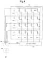
- FIG. 4 is a block diagram for describing a schematic configuration of the backlight 50 .
- the backlight 50 includes the LED drive circuit 520 , the power supply switching circuit 540 , the illuminating unit 560 , and an LED power source 580 .
- the substrate (LED substrate) that constitutes the illuminating unit 560 is logically divided into 16 (four vertical ⁇ four horizontal) areas. However, in general, the number of areas are contemplated to be equal or more than 1000 (for example, 1152 (24 ⁇ 48)).
- the illuminating unit 560 In the illuminating unit 560 , four power source lines PL 1 to PL 4 extending in the horizontal direction in FIG. 4 and four turn-on control lines SL 1 to SL 4 extending in the vertical direction in FIG. 4 are disposed. Each of the intersections of the four power source lines PL 1 to PL 4 and the four turn-on control lines SL 1 to SL 4 corresponds to one area, and one LED 562 is provided for each one of the 16 areas. In this manner, the illuminating unit 560 includes 16 LEDs 562 . These 16 LEDs are divided into four blocks (the first block BL 1 to the fourth block BL 4 ) as shown in FIG. 4 . By switching the supply destination of the power source voltage by the power supply switching circuit 540 , 16 LEDs 562 are driven on a block-by-block basis (on a row-by-row basis in the present embodiment).
- four LEDs 562 are included in one block, four channels (four turn-on control lines SL 1 to SL 4 ) are provided as channels for LED driving.
- driving turning on the LEDs 562 in the block
- driving is performed, for example, at the first block BL 1 , at the second block BL 2 , at the third block BL 3 , and at the fourth block BL 4 in this order in each frame period.
- the luminance of each LED 562 is controlled by the LED drive circuit 520 .
- FIG. 1 is a block diagram showing a functional configuration of the LED drive circuit 520 in the present embodiment.
- the LED drive circuit 520 includes, as shown in FIG. 1 , a control unit 521 , an LED data holding unit 522 , an operation setting data holding unit 523 , a liquid crystal driving frequency detection unit 524 , and a PWM/constant-current generating unit 525 .
- the LED data holding unit 522 is configured, for example, by a volatile register and holds the turn-on control data LD corresponding to respective LEDs 562 in the illuminating unit 560 .
- the turn-on control data LD is transmitted to the LED drive circuit 520 via a serial bus such as an Inter-Integrated Circuit (I2C) or a Serial Peripheral Interface (SPI).
- the turn-on control data LD transmitted to the LED drive circuit 520 includes address information, and the turn-on control data LD (information on the luminance of an LED 562 ) is written to a corresponding register in the LED data holding unit 522 based on the address information.
- the register for holding each turn-on control data LD is configured by a register for writing and a register for reading, and the turn-on control data LD written in the register for writing is transferred to the register for reading based on the vertical synchronization signal VS. Then, the turn-on control data LD is read out from the register for reading by the control unit 521 .
- the LED data holding unit 522 may be configured by a memory.
- each register constituting the LED data holding unit 522 is, for example, eight bits.
- the fact that the value held in a register is 255 indicates that an LED 562 corresponding to the register should be turned on at a duty ratio of 100%
- the fact that the value held in a register is 127 indicates that an LED 562 corresponding to the register should be turned on at a duty ratio of 50%.
- the operation setting data holding unit 523 is configured, for example, by a volatile register and holds the operation setting data SD specifying the operation of this LED drive circuit 520 .
- the operation setting data SD is also transmitted to the LED drive circuit 520 via a serial bus such as an I2C or a SPI.
- the operation setting data SD includes at least information on the number of blocks. It should be noted that the operation setting data SD is supplied from the local dimming control unit 40 to the LED drive circuit 520 at a timing, for example, immediately after start-up of the liquid crystal display device.
- the liquid crystal driving frequency detection unit 524 has a timer.
- the liquid crystal driving frequency detection unit 524 receives the vertical synchronization signal VS transmitted from the timing controller 10 , measures a length of one frame period based on the vertical synchronization signal VS by using the timer, and determines the liquid crystal driving frequency (the driving frequency of the display panel) FL based on the measurement result (the length of one frame period).
- Information on the liquid crystal driving frequency FL is supplied from the liquid crystal driving frequency detection unit 524 to the control unit 521 .
- the control unit 521 determines the lighting frequency of the LEDs 562 based on the information on the liquid crystal driving frequency FL supplied from the liquid crystal driving frequency detection unit 524 .
- the control unit 521 includes a look-up table 5212 that holds a correspondence relationship between the liquid crystal driving frequency and the lighting frequency of the LEDs 562 , schematically as shown in FIG. 5 .
- the lighting frequency of the LEDs 562 is changed based on this look-up table 5212 .
- the liquid crystal driving frequency becomes one-nth of that before change
- the lighting frequency of the LEDs 562 becomes n times of that before change.
- the control unit 521 determines the lighting frequency of the LEDs 562 by referring to the look-up table 5212 based on the information on the liquid crystal driving frequency FL supplied from the liquid crystal driving frequency detection unit 524 .
- the lighting frequency of the LEDs 562 is an integer multiple of the liquid crystal driving frequency in the example shown in FIG. 5 , the lighting frequency of the LEDs 562 is not limited to this. In addition, because flicker is more visible as the liquid crystal driving frequency is lower, it is preferable to increase the lighting frequency of the LEDs 562 as the liquid crystal driving frequency is lower.
- the switching control signal SWCTL for switching the register that is the read destination of the turn-on control data LD is generated based on a maximum turn-on time (a maximum time during which each LED 562 is capable of lighting by a single driving operation) Tmax that is obtained as described later. It should be noted that this switching control signal SWCTL is also used for switching the supply destination of the power source voltage by the power supply switching circuit 540 .
- T max 1/( NB ⁇ FB ) (1)
- the maximum turn-on time is obtained by the following equation (2).
- T max 1/(4 ⁇ 480) (2)
- the control unit 521 based on the lighting frequency determined by referring to the look-up table 5212 as described above and the information on the number of blocks included in the operation setting data SD, the maximum turn-on time Tmax is obtained by the above equation (1). Then, the control unit 521 generates the switching control signal SWCTL based on the maximum turn-on time Tmax and reads out the turn-on control data LD for LEDs which are lighting targets from the LED data holding unit 522 based on the switching control signal SWCTL. Further, the control unit 521 controls the operation of the PWM/constant-current generating unit 525 based on the read turn-on control data LD and the maximum turn-on time Tmax. Furthermore, the control unit 521 outputs the switching control signal SWCTL to the power supply switching circuit 540 . By this, the supply destination of the power source voltage can be switched every desired time in the power supply switching circuit 540 .
- FIG. 6 is a schematic diagram showing only components corresponding to one column of the PWM/constant-current generating unit 525 .
- the PWM/constant-current generating unit 525 includes a PWM signal generation circuit 5251 , a constant current source 5252 , and a switch (a transistor) 5253 .
- the constant current source 5252 functions such that the constant current flows through the turn-on control line SL.
- the switch 5253 switching between an ON state and an OFF state is performed based on the PWM signal PS outputted from the PWM signal generation circuit 5251 .
- the switch 5253 is in the ON state when the PWM signal PS is at a high level, and the switch 5253 is in the OFF state when the PWM signal PS is at a low level.
- the switch 5253 is in the ON state, the constant current flows through a corresponding turn-on control line SL (however, it is assumed that the power source voltage is supplied to any of the power source lines PL).
- the switch 5253 is in the OFF state, the constant current does not flow through the corresponding turn-on control line SL.
- the PWM signal generation circuit 5251 generates the PWM signal PS based on the turn-on control data LD and the maximum turn-on time Tmax.
- the PWM signal generation circuit 5251 when the turn-on control data LD is a data corresponding to a duty ratio of 50%, the PWM signal generation circuit 5251 generates the PWM signal PS that is maintained at the high level only a period of half of the maximum turn-on time Tmax.
- the LED 562 that is a lighting target emits light with luminance depending on a pulse width of the PWM signal PS.
- the functional configuration of the LED drive circuit 520 has been described in detail in the above, the functional configuration thereof is not limited to this. As long as a look-up table that holds a correspondence relationship between the liquid crystal driving frequency and the lighting frequency of the LEDs 562 are held and the liquid crystal driving frequency FL can be obtained based on the synchronization signal such as the vertical synchronization signal VS, the configuration of the LED drive circuit 520 is not particularly limited.
- each arrow given reference character 6 schematically represents the state in which writing to the pixel capacitance is performed from the first row to the last row.
- each arrow given reference character Ta represents a length of one frame period corresponding to the liquid crystal driving frequency of 60 Hz and each arrow given reference character Tb represents a length of one frame period corresponding to the liquid crystal driving frequency of 30 Hz.
- the liquid crystal driving frequency is 60 Hz. It should be noted that, in the LED drive circuit 520 , a length of one frame period is obtained by measuring a length of a period from a timing of falling of the vertical synchronization signal VS to a timing of next falling of the vertical synchronization signal VS, and then the liquid crystal driving frequency is determined based on the obtained length.
- the liquid crystal driving frequency is changed from 60 Hz to 30 Hz.
- a change of the liquid crystal driving frequency is not detected in the LED drive circuit 520 .
- the change of the liquid crystal driving frequency is detected in the LED drive circuit 520 based on a length of a period from time t 1 to time t 2 .
- the LED drive circuit 520 determines the lighting frequency of the LEDs 562 after change by referring to the above-described look-up table 5212 .
- the lighting frequency of the LEDs 562 is determined to be 480 Hz by referring to the look-up table 5212 (see FIG. 5 ).
- the LEDs 562 in the illuminating unit 560 are turned on with a lighting frequency of 480 Hz.
- the LEDs 562 which are driven as shown in FIG. 20 before time t 2 are driven as shown in FIG. 8 after time t 2 .
- the liquid crystal driving frequency is 30 Hz
- a length of one frame period is 1/30 seconds.
- the lighting frequency of the LEDs 562 is 480 Hz (that is, 16 times the liquid crystal driving frequency)
- each LED 562 is turned on 16 times during each frame period.
- the LED drive circuit 520 in the backlight 50 is provided with the liquid crystal driving frequency detection unit 524 that determines the liquid crystal driving frequency based on the vertical synchronization signal VS.
- the control unit 521 in the LED drive circuit 520 is provided with the look-up table 5212 that holds a correspondence relationship between the liquid crystal driving frequency and the lighting frequency of the LEDs 562 . Therefore, it is possible to change the lighting frequency of the LEDs 562 depending on change in the liquid crystal driving frequency.
- the look-up table 5212 holds the correspondence relationship such that the lighting frequency of the LEDs 562 is increased as the liquid crystal driving frequency is lower.
- the backlight 50 that can perform the time-sharing driving of LEDs 562 so as not to cause flicker even when the liquid crystal driving frequency changes dynamically.
- the look-up table 5212 holds the correspondence relationship such that when the liquid crystal driving frequency becomes one-nth of that before change, the lighting frequency of the LEDs 562 becomes n times of that before change.
- the correspondence relationship is not limited to this.
- the look-up table 5212 may hold the correspondence relationship such that when the liquid crystal driving frequency becomes lower than that before change, the lighting frequency of the LEDs 562 becomes equal to or higher than that before change.
- the lighting frequency of the LEDs 562 is maintained at 240 Hz. Further, for example, when the liquid crystal driving frequency changes from 60 Hz to 15 Hz, the lighting frequency of the LEDs 562 is changed from 240 Hz to 960 Hz.
- FIG. 10 is a block diagram showing an overall configuration of a liquid crystal display device according to the second embodiment.
- information on the liquid crystal driving frequency FL and information on the lighting frequency FB of the LEDs are transmitted from an external source (for example, a host) to the LED drive circuit 520 via a serial bus such as an I2C or a SPI. Based on these information, the LED drive circuit 520 turns on the LEDs 562 in the illuminating unit 560 on a block-by-block basis.
- FIG. 11 is a block diagram showing a functional configuration of the LED drive circuit 560 in the present embodiment.
- the LED drive circuit 560 in the present embodiment is provided with a frequency information holding unit 526 in place of the liquid crystal driving frequency detection unit 524 in the first embodiment.
- This frequency information holding unit 526 is configured by a volatile register or a memory and holds the information on the liquid crystal driving frequency FL transmitted from an external source and the information on the lighting frequency FB transmitted from an external source.
- the control unit 521 detects a change in the liquid crystal driving frequency based on the information held in the frequency information holding unit 526 .
- the control unit 521 read out the information on the lighting frequency FB of the LEDs 562 from the frequency information holding unit 526 .
- the control unit 521 obtains the maximum turn-on time Tmax in the same manner as in the first embodiment.
- the information on the lighting frequency FB that is the information required for the time-sharing driving of LEDs 562 , are supplied from an external source (for example, a host) to the LED drive circuit 520 .
- the LED drive circuit 520 turns on a plurality of LEDs 562 in the illuminating unit 560 in a time-sharing manner and on a block-by-block basis.
- the backlight 50 that can perform the time-sharing driving of LEDs 562 so as not to cause flicker even when the liquid crystal driving frequency changes dynamically.
- the combination of the liquid crystal driving frequency and the lighting frequency of the LEDs 562 not only predetermined combinations but also any combination can be adopted.
- a change of the liquid crystal driving frequency and a change of the lighting frequency of the LEDs 562 can be performed at the same timing.
Landscapes
- Physics & Mathematics (AREA)
- Nonlinear Science (AREA)
- Engineering & Computer Science (AREA)
- General Physics & Mathematics (AREA)
- Optics & Photonics (AREA)
- Crystallography & Structural Chemistry (AREA)
- Chemical & Material Sciences (AREA)
- Mathematical Physics (AREA)
- Computer Hardware Design (AREA)
- Theoretical Computer Science (AREA)
- Liquid Crystal Display Device Control (AREA)
- Liquid Crystal (AREA)
- Control Of Indicators Other Than Cathode Ray Tubes (AREA)
Abstract
Description
(4) Moreover, backlights according to several embodiments of the present invention are each a backlight including the configuration of above (2), wherein the correspondence relationship is held in the table such that when the driving frequency of the display panel becomes lower than that before change, the lighting frequency of the plurality of LEDs becomes equal to or higher than that before change.
(5) Moreover, backlights according to several embodiments of the present invention are each a backlight including the configuration of above (2), wherein
-
- a power supply switching circuit configured to switch a supply destination of a power source voltage for LED driving among the plurality of blocks, and
- an LED drive circuit configured to control a time length for supplying an LED that is a lighting target with a current, by using a PWM signal,
-
- a plurality of LED units divided into a plurality of blocks, each of the plurality of LED units including one or more LEDs, and
- a turn-on control circuit configured to turn on the plurality of LEDs in a time-sharing manner and on a block-by-block basis, and
Tmax=1/(NB×FB) (1)
Tmax=1/(4×480) (2)
Claims (5)
Priority Applications (1)
| Application Number | Priority Date | Filing Date | Title |
|---|---|---|---|
| US16/785,925 US10877315B2 (en) | 2019-02-15 | 2020-02-10 | Backlight and display device provided with same |
Applications Claiming Priority (2)
| Application Number | Priority Date | Filing Date | Title |
|---|---|---|---|
| US201962806673P | 2019-02-15 | 2019-02-15 | |
| US16/785,925 US10877315B2 (en) | 2019-02-15 | 2020-02-10 | Backlight and display device provided with same |
Publications (2)
| Publication Number | Publication Date |
|---|---|
| US20200264476A1 US20200264476A1 (en) | 2020-08-20 |
| US10877315B2 true US10877315B2 (en) | 2020-12-29 |
Family
ID=72040627
Family Applications (1)
| Application Number | Title | Priority Date | Filing Date |
|---|---|---|---|
| US16/785,925 Active US10877315B2 (en) | 2019-02-15 | 2020-02-10 | Backlight and display device provided with same |
Country Status (1)
| Country | Link |
|---|---|
| US (1) | US10877315B2 (en) |
Families Citing this family (4)
| Publication number | Priority date | Publication date | Assignee | Title |
|---|---|---|---|---|
| KR20230156205A (en) * | 2022-05-04 | 2023-11-14 | 삼성디스플레이 주식회사 | Display apparatus and method of operating the same |
| CN117292655A (en) * | 2022-06-17 | 2023-12-26 | 苏州佳世达电通有限公司 | Backlight device for improving dynamic blur, operating method and display device |
| US12437707B2 (en) * | 2023-09-27 | 2025-10-07 | Creeled, Inc. | Pseudo-exponential encoding for light-emitting devices and related methods |
| WO2026019074A1 (en) * | 2024-07-15 | 2026-01-22 | 삼성전자주식회사 | Display apparatus |
Citations (4)
| Publication number | Priority date | Publication date | Assignee | Title |
|---|---|---|---|---|
| WO2007017797A2 (en) | 2005-08-09 | 2007-02-15 | Koninklijke Philips Electronics N. V. | Liquid crystal display comprising a scanning backlight |
| JP2011013558A (en) | 2009-07-03 | 2011-01-20 | Sharp Corp | Liquid crystal display device |
| US20120098876A1 (en) * | 2009-07-03 | 2012-04-26 | Sharp Kabushiki Kaisha | Liquid Crystal Display Device And Light Source Control Method |
| US20120169801A1 (en) * | 2010-12-31 | 2012-07-05 | Joung-Woo Lee | Method and circuit for synchronizing input and output synchronizing signals, backlight driver in liquid crystal display device using the same, and method for driving the backlight driver |
-
2020
- 2020-02-10 US US16/785,925 patent/US10877315B2/en active Active
Patent Citations (5)
| Publication number | Priority date | Publication date | Assignee | Title |
|---|---|---|---|---|
| WO2007017797A2 (en) | 2005-08-09 | 2007-02-15 | Koninklijke Philips Electronics N. V. | Liquid crystal display comprising a scanning backlight |
| US20100134521A1 (en) * | 2005-08-09 | 2010-06-03 | Koninklijke Philips Electronics, N.V. | Device comprising a liquid crystal display |
| JP2011013558A (en) | 2009-07-03 | 2011-01-20 | Sharp Corp | Liquid crystal display device |
| US20120098876A1 (en) * | 2009-07-03 | 2012-04-26 | Sharp Kabushiki Kaisha | Liquid Crystal Display Device And Light Source Control Method |
| US20120169801A1 (en) * | 2010-12-31 | 2012-07-05 | Joung-Woo Lee | Method and circuit for synchronizing input and output synchronizing signals, backlight driver in liquid crystal display device using the same, and method for driving the backlight driver |
Also Published As
| Publication number | Publication date |
|---|---|
| US20200264476A1 (en) | 2020-08-20 |
Similar Documents
| Publication | Publication Date | Title |
|---|---|---|
| US20200051484A1 (en) | Backlight device and display device provided with same | |
| US10877315B2 (en) | Backlight and display device provided with same | |
| US10891895B2 (en) | Light emitting device, display device, and LED display device | |
| CN101105920B (en) | Liquid crystal display device, driving control circuit and driving method used in same device | |
| US8531384B2 (en) | Driving method for local dimming of liquid crystal display device and apparatus using the same | |
| KR20050051501A (en) | Field sequential liquid crystal lidplay | |
| US10935843B2 (en) | Backlight and display device provided with same | |
| JP2008249780A (en) | Liquid crystal display device | |
| KR20070003393A (en) | Power control device and method of display module | |
| US20080007573A1 (en) | Display device and display system employing same | |
| US7173588B2 (en) | Matrix display device having switching circuit for selecting either a picture voltage or a pre-write voltage for picture elements | |
| US7602362B2 (en) | Liquid crystal display device and method for driving the same | |
| KR20110035836A (en) | LCD Display | |
| KR101314212B1 (en) | Scanning backlight type Liquid Crystal Display Device and driving method of the same | |
| US12267922B2 (en) | Light-emitting device, display device, and LED display device | |
| KR101635220B1 (en) | Liquid crystal display and driving method thereof | |
| KR20150033213A (en) | Back light unit and liquid crystal display device using the same and driving method thereof | |
| CN100390619C (en) | Liquid crystal display device | |
| KR102458604B1 (en) | Liquid crystal display device and method of driving the same | |
| US20100045710A1 (en) | Backlight apparatus and a liquid crystal display including the same | |
| KR20090002730A (en) | Back light unit, liquid crystal display using same and driving method thereof | |
| KR20120008185A (en) | LCD Display | |
| US20160086576A1 (en) | Display device including a backlight unit | |
| KR100599757B1 (en) | LCD and its driving method | |
| KR101747713B1 (en) | Back light unit and liquid crystal display device using the same |
Legal Events
| Date | Code | Title | Description |
|---|---|---|---|
| AS | Assignment |
Owner name: SHARP KABUSHIKI KAISHA, JAPAN Free format text: ASSIGNMENT OF ASSIGNORS INTEREST;ASSIGNOR:YASHIKI, MASAFUMI;REEL/FRAME:051768/0719 Effective date: 20190208 |
|
| FEPP | Fee payment procedure |
Free format text: ENTITY STATUS SET TO UNDISCOUNTED (ORIGINAL EVENT CODE: BIG.); ENTITY STATUS OF PATENT OWNER: LARGE ENTITY |
|
| STPP | Information on status: patent application and granting procedure in general |
Free format text: RESPONSE TO NON-FINAL OFFICE ACTION ENTERED AND FORWARDED TO EXAMINER |
|
| STPP | Information on status: patent application and granting procedure in general |
Free format text: NOTICE OF ALLOWANCE MAILED -- APPLICATION RECEIVED IN OFFICE OF PUBLICATIONS |
|
| STPP | Information on status: patent application and granting procedure in general |
Free format text: PUBLICATIONS -- ISSUE FEE PAYMENT VERIFIED |
|
| STCF | Information on status: patent grant |
Free format text: PATENTED CASE |
|
| MAFP | Maintenance fee payment |
Free format text: PAYMENT OF MAINTENANCE FEE, 4TH YEAR, LARGE ENTITY (ORIGINAL EVENT CODE: M1551); ENTITY STATUS OF PATENT OWNER: LARGE ENTITY Year of fee payment: 4 |