US10868116B2 - Circuit structure and method for reducing electronic noises - Google Patents
Circuit structure and method for reducing electronic noises Download PDFInfo
- Publication number
- US10868116B2 US10868116B2 US15/940,617 US201815940617A US10868116B2 US 10868116 B2 US10868116 B2 US 10868116B2 US 201815940617 A US201815940617 A US 201815940617A US 10868116 B2 US10868116 B2 US 10868116B2
- Authority
- US
- United States
- Prior art keywords
- gate stack
- feature
- active region
- region
- disposed
- Prior art date
- Legal status (The legal status is an assumption and is not a legal conclusion. Google has not performed a legal analysis and makes no representation as to the accuracy of the status listed.)
- Active, expires
Links
Images


Classifications
-
- H01L29/0653—
-
- H—ELECTRICITY
- H10—SEMICONDUCTOR DEVICES; ELECTRIC SOLID-STATE DEVICES NOT OTHERWISE PROVIDED FOR
- H10D—INORGANIC ELECTRIC SEMICONDUCTOR DEVICES
- H10D62/00—Semiconductor bodies, or regions thereof, of devices having potential barriers
- H10D62/10—Shapes, relative sizes or dispositions of the regions of the semiconductor bodies; Shapes of the semiconductor bodies
- H10D62/113—Isolations within a component, i.e. internal isolations
- H10D62/115—Dielectric isolations, e.g. air gaps
- H10D62/116—Dielectric isolations, e.g. air gaps adjoining the input or output regions of field-effect devices, e.g. adjoining source or drain regions
-
- H01L29/1041—
-
- H01L29/66492—
-
- H01L29/6659—
-
- H01L29/7833—
-
- H—ELECTRICITY
- H10—SEMICONDUCTOR DEVICES; ELECTRIC SOLID-STATE DEVICES NOT OTHERWISE PROVIDED FOR
- H10D—INORGANIC ELECTRIC SEMICONDUCTOR DEVICES
- H10D30/00—Field-effect transistors [FET]
- H10D30/01—Manufacture or treatment
- H10D30/021—Manufacture or treatment of FETs having insulated gates [IGFET]
- H10D30/022—Manufacture or treatment of FETs having insulated gates [IGFET] having lightly-doped source or drain extensions selectively formed at the sides of the gates
-
- H—ELECTRICITY
- H10—SEMICONDUCTOR DEVICES; ELECTRIC SOLID-STATE DEVICES NOT OTHERWISE PROVIDED FOR
- H10D—INORGANIC ELECTRIC SEMICONDUCTOR DEVICES
- H10D30/00—Field-effect transistors [FET]
- H10D30/01—Manufacture or treatment
- H10D30/021—Manufacture or treatment of FETs having insulated gates [IGFET]
- H10D30/0223—Manufacture or treatment of FETs having insulated gates [IGFET] having source and drain regions or source and drain extensions self-aligned to sides of the gate
- H10D30/0227—Manufacture or treatment of FETs having insulated gates [IGFET] having source and drain regions or source and drain extensions self-aligned to sides of the gate having both lightly-doped source and drain extensions and source and drain regions self-aligned to the sides of the gate, e.g. lightly-doped drain [LDD] MOSFET or double-diffused drain [DDD] MOSFET
-
- H—ELECTRICITY
- H10—SEMICONDUCTOR DEVICES; ELECTRIC SOLID-STATE DEVICES NOT OTHERWISE PROVIDED FOR
- H10D—INORGANIC ELECTRIC SEMICONDUCTOR DEVICES
- H10D30/00—Field-effect transistors [FET]
- H10D30/01—Manufacture or treatment
- H10D30/021—Manufacture or treatment of FETs having insulated gates [IGFET]
- H10D30/028—Manufacture or treatment of FETs having insulated gates [IGFET] of double-diffused metal oxide semiconductor [DMOS] FETs
- H10D30/0281—Manufacture or treatment of FETs having insulated gates [IGFET] of double-diffused metal oxide semiconductor [DMOS] FETs of lateral DMOS [LDMOS] FETs
-
- H—ELECTRICITY
- H10—SEMICONDUCTOR DEVICES; ELECTRIC SOLID-STATE DEVICES NOT OTHERWISE PROVIDED FOR
- H10D—INORGANIC ELECTRIC SEMICONDUCTOR DEVICES
- H10D30/00—Field-effect transistors [FET]
- H10D30/60—Insulated-gate field-effect transistors [IGFET]
- H10D30/601—Insulated-gate field-effect transistors [IGFET] having lightly-doped drain or source extensions, e.g. LDD IGFETs or DDD IGFETs
- H10D30/603—Insulated-gate field-effect transistors [IGFET] having lightly-doped drain or source extensions, e.g. LDD IGFETs or DDD IGFETs having asymmetry in the channel direction, e.g. lateral high-voltage MISFETs having drain offset region or extended drain IGFETs [EDMOS]
-
- H—ELECTRICITY
- H10—SEMICONDUCTOR DEVICES; ELECTRIC SOLID-STATE DEVICES NOT OTHERWISE PROVIDED FOR
- H10D—INORGANIC ELECTRIC SEMICONDUCTOR DEVICES
- H10D30/00—Field-effect transistors [FET]
- H10D30/60—Insulated-gate field-effect transistors [IGFET]
- H10D30/64—Double-diffused metal-oxide semiconductor [DMOS] FETs
- H10D30/65—Lateral DMOS [LDMOS] FETs
-
- H—ELECTRICITY
- H10—SEMICONDUCTOR DEVICES; ELECTRIC SOLID-STATE DEVICES NOT OTHERWISE PROVIDED FOR
- H10D—INORGANIC ELECTRIC SEMICONDUCTOR DEVICES
- H10D62/00—Semiconductor bodies, or regions thereof, of devices having potential barriers
- H10D62/10—Shapes, relative sizes or dispositions of the regions of the semiconductor bodies; Shapes of the semiconductor bodies
- H10D62/17—Semiconductor regions connected to electrodes not carrying current to be rectified, amplified or switched, e.g. channel regions
- H10D62/213—Channel regions of field-effect devices
- H10D62/221—Channel regions of field-effect devices of FETs
- H10D62/235—Channel regions of field-effect devices of FETs of IGFETs
- H10D62/299—Channel regions of field-effect devices of FETs of IGFETs having lateral doping variations
Definitions
- An integrated circuit includes various devices (e.g., transistors, diodes, and resistors) connected together and configured to work as a functional circuit.
- FETs field effect transistors
- different materials come into contact in a channel, creating various interface areas.
- a channel has a horizontal interface with an overlaying gate dielectric layer and vertical interfaces with isolation features that extend into the channel from the sides.
- charge carriers electrosprays
- the fluctuation in carrier mobility tends to generate or increase electronic noises, such as flicker noise and random telegraph signal (RTS) noise.
- Flicker noise (sometimes called 1/f noise or pink noise) is a low frequency noise that may exhibit an inverse frequency power density curve.
- RTS noise sometimes called burst noise, popcorn noise, impulse noise, bi-stable noise
- thinning down the gate dielectric thickness may reduce noises, a thinner gate dielectric layer may degrade performance of a transistor, for example, in high-voltage applications.
- a new device structure is desired to address the above concerns in high-voltage and other transistor applications.
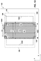
- FIG. 1A is a top view of a semiconductor device structure according to various embodiments of the present disclosure.
- FIGS. 1B and 1C are sectional views of the semiconductor structure of FIG. 1A along the dashed lines AA′ and BB′, respectively, according to various embodiments.
- FIG. 1D is a further top view of the semiconductor device structure according to various embodiments.
- FIG. 2 is a flowchart of a method making a semiconductor structure according to various embodiments.
- FIGS. 3A, 3B, 3C, 3D, and 3E are sectional views of a semiconductor structure during various intermediate stages of fabrication, according to various embodiments.
- FIG. 4 is a sectional view of a semiconductor structure according to various embodiments.
- FIG. 5 is a sectional view of a semiconductor structure according to various embodiments.
- first and second features are formed in direct contact
- additional features may be formed between the first and second features, such that the first and second features may not be in direct contact
- present disclosure may repeat reference numerals and/or letters in the various examples. This repetition is for the purpose of simplicity and clarity and does not in itself dictate a relationship between the various embodiments and/or configurations discussed. It is to be understood that the following disclosure provides many different embodiments, or examples, for implementing different features of various embodiments. Specific examples of components and arrangements are described below to simplify the present disclosure. These are, of course, merely examples and are not intended to be limiting.
- spatially relative terms such as “beneath,” “below,” “lower,” “above,” “upper” and the like, may be used herein for ease of description to describe one element or feature's relationship to another element(s) or feature(s) as illustrated in the figures.
- the spatially relative terms are intended to encompass different orientations of the device in use or operation in addition to the orientation depicted in the figures. For example, if the device in the figures is turned over, elements described as being “below” or “beneath” other elements or features would then be oriented “above” the other elements or features.
- the exemplary term “below” can encompass both an orientation of above and below.
- the apparatus may be otherwise oriented (rotated 90 degrees or at other orientations) and the spatially relative descriptors used herein may likewise be interpreted accordingly.
- FIG. 1A is a schematic top view of a semiconductor structure (or device, or work piece) 100 constructed according to various aspects of the present disclosure in one embodiment.
- FIG. 1B is a schematic sectional view of the semiconductor structure 100 along the dashed line AA′
- FIG. 1C is a schematic sectional view of the semiconductor structure 100 along the dashed line BB′.
- the semiconductor structure 100 is formed on fin active regions and includes fin field-effect transistors (FinFETs).
- the semiconductor structure 100 is formed on flat active regions and includes a plain field-effect transistor (FET).
- the FET may be n-type (nFET) or p-type (pFET).
- the semiconductor structure 100 is part of an integrated circuit (IC) device, and it includes a substrate 102 .
- the substrate 102 may be a bulk silicon substrate.
- the substrate 102 may include an elementary semiconductor (e.g., silicon or germanium in a crystalline structure), a compound semiconductor (e.g., silicon germanium, silicon carbide, gallium arsenic, gallium phosphide, indium phosphide, indium arsenide, and/or indium antimonide), or combinations thereof.
- the substrate 102 may also include a silicon-on-insulator (SOI) substrate, which is fabricated using separation by implantation of oxygen (SIMOX), wafer bonding, and/or other suitable methods.
- SOI silicon-on-insulator
- the substrate 102 includes one or more isolation regions such as isolation region 104 formed on the substrate 102 .
- the isolation region 104 at least partially surrounds and defines various active regions, such as active region 106 , on the substrate 102 .
- the isolation region 104 utilizes isolation technology, such as local oxidation of silicon (LOCOS) and/or shallow trench isolation (STI), to electrically isolate the various active regions.
- LOC local oxidation of silicon
- STI shallow trench isolation
- different parts of the isolation region 104 are referred to as isolation features (e.g., isolation features 104 A and 104 B shown in FIGS. 1B and 1C ).
- the isolation region 104 includes silicon oxide, silicon nitride, silicon oxynitride, other suitable dielectric materials, or combinations thereof.
- the isolation region 104 is formed by any suitable process.
- forming STI features includes using a lithography process to expose a portion of the substrate, etching a trench in the exposed portion of the substrate (for example, by using a dry etching and/or wet etching), filling the trench (for example, by using a chemical vapor deposition process) with one or more dielectric materials, and planarizing the substrate and removing excessive portions of the dielectric material(s) by a polishing process, such as chemical mechanical polishing (CMP).
- the filled trench may have a multi-layer structure, such as a thermal oxide liner layer filled with silicon nitride or silicon oxide.
- Active regions are those regions with semiconductor surface where various doped features are formed and configured as components of one or more devices, such as a diode, a transistor, and/or other suitable devices.
- the active region 106 may include a semiconductor material similar to that of the bulk semiconductor material of the substrate 102 (e.g., silicon) or a different semiconductor material, such as silicon germanium (SiGe), silicon carbide (SiC), or multiple semiconductor material layers (e.g., alternating silicon and silicon germanium layers) formed on the substrate 102 by epitaxial growth, for performance enhancement, such as strain effect to increase carrier mobility.
- the isolation region 104 separates the active region 106 from other active regions (not shown in FIGS. 1A-1C ).
- the active region 106 is three dimensional, such as a fin active region extending above the substrate 102 .
- the fin active region may be formed by selective etching to recessing the isolation region 104 , or by selective epitaxial growth with a semiconductor that is the same or different from that of the substrate 102 , or a combination both methods.
- the semiconductor substrate 102 includes various doped features—such as n-type doped wells, p-type doped wells, source and drain, other doped features, or combinations thereof—configured to form various device components or structures.
- the semiconductor substrate 102 includes a doped well 110 of a first-type.
- the doped well 110 is a p-well (i.e., doped with a p-type dopant).
- the dopant (such as boron) in the doped well 110 may be introduced to the substrate 102 by ion implantation or other suitable technique.
- the doped well 110 may be formed by a procedure that includes first forming a patterned mask with an opening on the substrate 102 , where the opening defines the region for the doped well 110 ; and then performing an ion implantation to introduce the dopant into the substrate 102 using the patterned mask as an implantation mask.
- the patterned mask may be a patterned resist layer formed by lithography or a pattern hard mask formed by lithography process and etching.
- the doped well 110 encloses the active region 106 in the top view, as illustrated in FIG. 1A , so as to ensure full doping of the active region 106 with the first type dopant.
- the semiconductor structure 100 further includes a gate stack 114 having a length oriented in the X direction and a width oriented in the Y direction.
- the Y direction is orthogonal to the X direction
- the X and Y directions define the top surface of the substrate 102 .
- the top surface has a normal direction along the Z direction, which is orthogonal to both X and Y directions.
- the gate stack 114 covers part of the active region 106 but does not extend to any other active region. As shown in the top view in FIG. 1A , the four corners of the gate stack 114 extends beyond the active region 106 into the isolation region 104 .
- the gate stack 114 includes a gate dielectric layer 116 and a gate electrode 120 disposed thereon.
- the gate dielectric layer 116 includes a dielectric material such as silicon oxide or a high-k material such as metal oxide, metal nitride or metal oxynitride.
- the high-k dielectric material includes metal oxide such as ZrO 2 , Al 2 O 3 , and HfO 2 —formed by a suitable method, such as metal organic chemical vapor deposition (MOCVD), physical vapor deposition (PVD), atomic layer deposition (ALD), or molecular beam epitaxy (MBE).
- MOCVD metal organic chemical vapor deposition
- PVD physical vapor deposition
- ALD atomic layer deposition
- MBE molecular beam epitaxy
- the gate dielectric layer 116 may further include an interfacial layer interposed between the semiconductor substrate 102 and the high-k dielectric material.
- the interfacial layer includes silicon oxide formed by ALD, thermal oxidation, or ultraviolet-ozone oxidation.
- a thickness of the gate dielectric layer 116 can be tuned to optimize device performance. For example, high-voltage applications may require a relatively thick gate dielectric layer 116 , but the thickness may increase noises. Thus, as described in details below, other aspects of the gate stack 114 are designed to minimize noise issues while maintaining the viability of semiconductor structure 100 for high-voltage applications.
- the gate electrode 120 includes metal, such as aluminum, copper, tungsten, metal silicide, metal alloy, doped poly-silicon, other proper conductive material or a combination thereof.
- the gate electrode 120 may include multiple conductive films designed such as a capping layer, a work function metal layer, a blocking layer and a filling metal layer (such as aluminum or tungsten).
- the multiple conductive films are designed for work function matching to nFET (or pFET).
- the gate electrode 120 for nFET includes a work function metal with a composition designed with a work function equal 4.2 electronic volts (eV) or less.
- the gate electrode for pFET includes a work function metal with a composition designed with a work function equal 5.2 eV or greater.
- the work function metal layer for nFET includes tantalum, titanium aluminum, titanium aluminum nitride or a combination thereof.
- the work function metal layer for pFET includes titanium nitride, tantalum nitride or a combination thereof.
- the gate stack 114 may be formed by various deposition techniques following a proper procedure, such as a gate-last process, wherein a dummy gate is first formed and is then replaced by a metal gate after forming source and drain.
- the gate stack 114 may be formed by high-k-last process, where both the gate dielectric material layer 116 and the gate electrode 120 are replaced by a high-k dielectric material and metal, respectively, after forming source and drain.
- the gate stack 114 may further include on its sidewalls a gate spacer 122 .
- the gate spacer 122 is considered as attached to the gate stack 114 and separating the gate stack 114 from other structures such as the isolation region 104 .
- the spacer 122 includes silicon oxide, silicon nitride, silicon oxynitride, other suitable dielectric material, or a combination thereof.
- the spacer 122 may have a multilayer structure and may be formed by depositing dielectric material and then anisotropic etching, such as plasma etching.
- anisotropic etching such as plasma etching.
- One exemplary gate stack 114 and the method of making the same are further described below in accordance with some embodiments.
- the semiconductor structure 100 includes a channel region 124 defined on the active region 106 and underlying the gate stack 114 .
- the channel region 124 may be tuned for proper threshold voltage or other parameters by ion implantation.
- the channel region 124 has a same type of dopant to that of the doped well 110 but at a greater concentration, depending on the application and device specification. In the present example for nFET, the channel region 124 is doped with a p-type dopant.
- the semiconductor structure 100 further includes a source 126 and a drain 128 formed on the active region 106 on opposite sides of the gate stack 114 .
- An N-type doped region functions as the source 126 (or source feature) and another N-type doped region functions as the drain 128 (or drain feature).
- the source 126 and the drain 128 are doped with an N-type impurity such as phosphorous for an nFET.
- the source 126 and the drain 128 may be formed by ion implantation and/or diffusion. Other processing steps may be further included to form the source 126 and the drain 128 . For example, a rapid thermal annealing (RTA) process may be used to activate the implanted dopant.
- RTA rapid thermal annealing
- the source 126 and the drain 128 may have different doping profiles formed by multi-step implantation. For example, additional doping features such as light doped drain or double diffused drain may be included. Also, the source 126 and the drain 128 may have different structures, such as raised, recessed, or strained. For example, if the active region 106 is a fin active region, the formation of the source 126 and the drain 128 may include: an etching process to recess source and drain regions; an epitaxial growth process to form epitaxial source and drain with in-situ doping; and an annealing process for activation. The channel region 124 is interposed between the source 126 and the drain 128 .
- FIGS. 1A-1C illustrate the source 126 and the drain 128 as somewhat symmetrically disposed on both sides of the channel region 124
- the source 126 and the drain 128 are configured asymmetrically (e.g., for some high voltage applications).
- the drain 128 as a high voltage is applied during the field applications, may be spaced further away from the gate stack 114 , thus the high voltage is able to be distributed in the region between the gate and the drain 128 to reduce high voltage damages to the device.
- the source 126 may be configured closer to the gate stack 114 , such that an edge of the source 126 is aligned to an edge of the gate stack 114 , as illustrated in FIG. 1A .
- the formation of the source 126 and the drain 128 may include forming a patterned mask to define source and drain regions, and implantation or epitaxial growth to form the source 126 and the drain 128 .
- the source 126 may further include silicide on its top surface to reduce contact resistance.
- silicide on the source 126 may be formed by a self-aligned silicide procedure that further includes depositing a metal (such as nickel, cobalt, titanium or other suitable metal) on the source; annealing to react the metal with silicon of the source 126 to form metal silicide; and etching to remove unreacted metal.
- the source 126 and the drain 128 are epitaxially grown.
- the epitaxial source and drain may be formed by selective epitaxial growth for straining effect with enhanced carrier mobility and device performance.
- the source 126 and the drain 128 are formed by one or more epitaxial growth process, where silicon (Si) features, silicon germanium (SiGe) features, silicon carbide (SiC) features, and/or other suitable semiconductor features are grown in a crystalline state on the active region 106 within source and drain regions (such as defined by a patterned hard mask).
- an etching process is applied to recess portions of the active region 106 within the source and drain regions before the epitaxial growth process.
- the etching process may also remove any dielectric material disposed on the source/drain regions, such as during the formation of the gate sidewall features.
- Suitable epitaxy processes include CVD deposition techniques (e.g., vapor-phase epitaxy (VPE) and/or ultra-high vacuum CVD (UHV-CVD), molecular beam epitaxy, and/or other suitable processes.
- the source 126 and the drain 128 may be doped in-situ during the epitaxy process by introducing doping species including: n-type dopants such as phosphorus or arsenic, or p-type dopants, such as boron or BF 2 for pFET.
- the source 126 and the drain 128 are not doped in-situ, an implantation process (i.e., a junction implant process) is performed to introduce the corresponding dopant into the source 126 and the drain 128 .
- the raised source and drain are formed by epitaxial growth with more than one semiconductor material layers. For example, a silicon germanium layer is epitaxially grown on the substrate 102 within the source and drain regions and a silicon layer is then epitaxially grown on the silicon germanium layer.
- the semiconductor structure 100 further includes contact features, such as contact pads 130 A and 130 B, formed on various doped regions. As an example illustrated in FIG. 1A , two contact pads 130 A are formed on the source 126 , and two contact pads 130 B are formed on the drain 128 . The source 126 and the drain 128 may use any suitable number of contact features or pads. Contact pad(s) for the gate stack 114 may be routed to the gate stack 114 via other structures or may be directly disposed on the gate stack 114 (e.g., when there is insufficient room to form its contact pads outside of the gate stack 114 ).
- the semiconductor structure 100 functions as a FET (an nFET in the present example).
- the source 126 , the drain 128 , the channel region 124 , and the gate stack 114 constitute the nFET.
- a channel has significant vertical interface areas with isolation features that extend into the channel from the sides. That is because the entire width of a gate stack in the Y direction laterally extends well into the isolation features.
- charge carriers electrosprays
- the fluctuation in carrier mobility tends to generate or increase electronic noises, such as flicker noise and random telegraph signal (RTS) noise.
- one or more of the active region 106 , the isolation region 104 , and the gate stack 114 is modified to reduce or eliminate such noises by reducing the amount of lateral overlap between the gate stack 114 and the isolation region 104 . In other words, an edge of the isolation region 104 is moved further away from the channel region 124 by reducing an overlapping area between the isolation region 104 and the overlaying gate stack 114 .
- the active region 106 may be divided into three rectangular portions arranged in the X direction: a middle portion 106 A, a left portion 106 B, and a right portion 106 C, where the middle portion 106 A is sandwiched by the left portion 106 B and the right portion 106 C.
- the middle portion 106 A is wider in the Y direction than the left portion 106 B and the right portion 106 C. Therefore, from the perspective of a top view such as FIG. 1A , the middle portion 106 A laterally extends beyond the gate stack 114 in the Y direction.
- corner portions 114 A, 114 B, 114 C, and 114 D still laterally extend beyond the active region 106 into the isolation region 104 .
- the reason that the corner portions 114 A- 114 D reach into the isolation region 104 is to prevent any leakage current from circumventing the gate stack 114 between the source 126 and the drain 128 .
- the gate stack 114 may no longer effectively control the channel region 124 since a leakage current may flow between the source and drain outside the gate stack 114 .
- edges of the gate stack 114 laterally “intersect” edges of the gate stack 114 (although they have different vertical positions as shown in FIGS. 1B and 1C ).
- one or more doping features 117 may be formed at edges of the middle portion 106 A in order to further reduce operational noises.
- Each doping feature 117 uses the same dopant type with the channel region 124 but has a higher (e.g., 20 times higher) doping concentration.
- the higher doping concentration changes the interfacial dynamics between the channel region 124 and the edge of the isolation region 104 , thereby effectively reducing the impact of the isolation region 104 on current conduction in the channel region 124 .
- Such a configuration reduces noises generated by an interface area between the edge of the isolation region 104 and an upper portion of the channel region 124 where most current conduction occurs.
- each doping feature 117 may include multiple features with varying doping concentrations.
- each doping feature 117 includes a low density doped (LDD) feature 118 and a high density doped (HDD) feature 119 .
- LDD and HDD features may be called NLDD and NHDD features, respectively.
- the LDD and HDD features may be called PLDD and PHDD features, respectively.
- the LDD feature 118 has a doping concentration at least twice as high as that of a channel region 124 underneath the gate stack 114 .
- the HDD feature 119 includes a doping concentration that is at least 10 times as high as that of the LDD feature 118 .
- the LDD feature 118 is disposed underneath the spacer 122 to separate an edge portion ( 114 E or 114 F) of the gate stack 114 from the isolation region 106 .
- the HDD feature 119 is disposed to further separate the LDD feature 118 and the spacer 122 from the isolation region 104 .
- the LDD feature 118 is relatively shallower than the HDD feature 119 . Together, the LDD feature 118 and the HDD feature 119 effectively block an edge of the isolation region 104 from affecting current conduction in the upper portion of the channel region 124 .
- FIG. 1D is a simplified version of FIG. 1A with additional dimensional notations.
- the gate stack 114 has a length L 1 in the X direction and a width W 1 in the Y direction (not accounting thickness of the spacer 122 ).
- the middle portion of the active region 106 A has a length L 2 in the X direction and a width W 2 in the Y direction.
- the corner portions 114 A and 114 B have lengths c 1 and c 2 , respectively, in the X direction.
- L 2 may be as close to L 1 as practicable. In some embodiments, L 2 is no less than 95% of L 1 . In other words, the total length of the corner portions 114 A and 114 B (c 1 +c 2 ) only accounts for no more than 5% of the gate stack length (L 2 ). In alternative embodiments, however, L 2 may be much shorter than L 1 (e.g., between 5%-50% of L 1 ).
- the middle portion 106 A laterally extends beyond the gate stack 114 by a first distance (a) in the Y direction
- the four corner portions 114 A- 114 D laterally extend beyond the left and right portions 106 B and 106 C by a second distance (b) in the Y direction.
- an edge of the gate stack 114 running in the X direction is disposed at about the mid-point in the Y direction between an edge of the middle portion 106 a and edges of the left and right portions 106 B and 106 C.
- the source 126 and the drain 128 are separated by the channel region 124 with a channel width in the Y direction (which may be roughly the same with W 1 ) and a channel length in the X direction (L 3 , which may be different from L 1 when the source 126 or the drain 128 is not aligned with edges of the gate stack 114 ). Therefore, the channel width in the Y direction may be less than W 2 (i.e., the middle portion 106 A laterally protrudes or sticks out of the channel region 124 ).
- the corner portions 114 A- 114 D may have rounded or straight corners.
- FIG. 1D shows that the corner portions 114 A- 114 D have a normal angle of 90 degrees (denoted as angle “M”), but this angle may have another value.
- the active region 106 may or may not have a normal angle (denoted as angle “N”) at the juncture between its middle portion 106 A and left and right portions 106 B or 106 C.
- angle “M” normal angle of 90 degrees
- N normal angle
- methods of measuring the various dimensions disclosed herein may vary accordingly.
- the various FET structures disclosed herein may have any suitable size or dimension.
- an FET when used for analog and radio frequency (RF) applications an FET may have relatively large sizes (e.g., at least hundreds of nanometers in width or length).
- a, b, c 1 , and c 2 shown in FIG. 1D may each be in the range of 0.03 to 0.3 micrometer (um).
- each of a, b, c 1 , and c 2 may be the same or may be different from one another.
- L 2 is 0.3 um or more (e.g., 0.3-1 um).
- FIG. 2 is a flowchart of the method 200 for making an IC device having an FET.
- the method 200 is described in connection with FIGS. 3A-3E , which are the same sectional view as FIG. 1B but represent intermediate stages of the semiconductor structure 100 before leading to the semiconductor structure 100 shown in FIG. 1B .
- a starting semiconductor structure is provided, which includes the substrate 102 , the isolation features 104 A and 104 B on the substrate 102 , and the active region 106 , as shown in FIG. 3A .
- the isolation features 104 A and 104 B at least partially surround and define the active region 106 .
- the formation of the isolation features 104 A and 104 B may include forming a patterned mask by lithography; etching the substrate 102 through the openings of the patterned mask to form trenches; filling the trench with one or more dielectric material; and performing a CMP process.
- the active region 106 may be three-dimensional, such as fin active regions.
- the operation 202 may further includes selective etching to recess the isolation features 104 A and 104 B or selective epitaxial growth to the active regions with one or more semiconductor material.
- the gate stack 114 is formed over the active region 106 .
- the gate stack 114 at this stage includes the gate dielectric layer 116 and the gate electrode layer 120 formed above the gate dielectric layer 116 .
- the gate dielectric layer 116 may include silicon oxide, high-k dielectric material, other suitable dielectric material, or a combination thereof.
- the gate electrode 120 includes any suitable conductive material, such as doped poly-silicon, metal, metal alloy, or metal silicide.
- the formation of the gate stack 114 may include a gate-last process, a high-k-last process, or other suitable procedure.
- two LDD features 118 are formed in the middle portion 106 A of the active region 106 , as shown in FIG. 3C .
- Each LDD feature 118 is disposed at an edge portion ( 114 E or 114 F) of the gate dielectric layer 116 and separates it from the isolation features 104 .
- Profiles of the LDD features 118 on two sides of the gate stack 114 may or may not be symmetrical. In some embodiments, only one side of the gate stack 114 has the LDD feature.
- the LDD feature 118 may be formed using any suitable technique, for example, by ion implantation.
- the LDD feature 118 has the same dopant type as the channel region 124 but has a doping concentration at least twice as high as that of the channel region 124 .
- the channel region 124 may have a doping concentration between 1-5*E13 (unit is per square centimeter), while the LDD feature 118 may have a doping concentration between 6-9*E13.
- the doping area may be designed to be relatively large (since doping is shallower on the edge of the doping area).
- the spacer 122 is formed on sidewalls of the gate stack directly above the LDD features 118 , as shown in FIG. 3D .
- the spacer 122 may or may not laterally reach into the isolation features 104 A and 104 B depending on its thickness.
- a portion of the spacer 122 is attached to a middle edge portion ( 114 E or 114 F) of the gate stack 114 that corresponds to the middle portion 106 A, so this portion of the spacer 122 does not laterally extend into the isolation features 104 .
- a thicker spacer 122 may laterally extend into the isolation features 104 .
- the spacer 122 includes one or more dielectric material, such as silicon oxide or silicon nitride.
- the LDD features 118 are formed before the formation of the spacer 122 , in some embodiments the LDD features 118 may be formed after the formation of the spacer 122 , e.g., using tilt angle implantation to extend underneath the spacer 122 .
- two HDD features 119 are formed as shown in FIG. 3E .
- the HDD features 119 separate the LDD features 118 and the spacer 122 from the isolation features 104 . Profiles of the HDD features 119 on two sides of the gate stack 114 may or may not be symmetrical.
- the HDD features 119 may be formed using any suitable techniques and processes. Note that the LDD features 118 and the HDD features 119 are formed using separate ion implantation processes, since the LDD features 118 are formed before forming the spacer 122 , while the HDD features 119 are formed after forming the spacer 122 .
- the HDD features 119 include a doping concentration that is at least 10 times as high as that of the LDD features 118 .
- the LDD feature 118 may have a doping concentration between 6-9*E13, and the HDD feature 119 may have a doping concentration no less than 1*E15.
- the dopant types for the LDD features 118 and the HDD features 119 are the same, but the doping materials may or may not be the same. Note that the channel region 124 , the LDD features 118 , and the HDD features 119 use the same dopant type that is opposite the dopant for the source 126 and the drain 128 .
- the doping area may be relatively large (since doping is shallower on the edge of the doping area), even possibly reaching into the LDD feature 118 and into the isolation region 106 (as shown in FIG. 1A and FIG. 3E ).
- the HDD feature 119 When the HDD feature 119 is doped on top of the LDD feature 118 , it converts the LDD feature 118 into the HDD feature 119 .
- the doping concentration within a doping feature may not be uniform, in which case the doping concentrations disclosed herein may be measured using practicable methods.
- the method 200 may additionally include other operations before, during or after the operations described above.
- the method 200 may include an operation to form the source 126 and the drain 128 in the active region 106 , where the source 126 and the drain 128 are interposed by the channel region 124 underlying the gate stack 114 .
- the source 126 and the drain 128 may be asymmetrically configured on opposite sides of the gate stack 114 in the X direction, where the drain 128 is spaced further away from the gate stack 114 while the source 126 is aligned to the edge of the gate stack.
- the formation of the source 126 and the drain 128 occurs after forming the spacer 122 , but may be before or after forming the HDD features 119 since they deal with different lateral regions of the semiconductor structure 100 .
- the method 200 may continue to form other structures—such as the contact pads 130 A and 130 B—before forming a functional IC device.
- FIG. 3E shows HDD features 119 formed on both sides of the gate stack 114 (in the Y direction).
- the LLD features 118 but not HDD features 119 are formed on both sides of the gate stack 114 .
- the LLD features 118 may be relatively wider such that covers the entire distance between the gate stack 114 and the isolation features 104 .
- Such a configuration effectively blocks the edges of the isolation features 104 A and 104 B from an upper section of the channel region 124 , where most of the current conduction takes place.
- the LLD features 118 are formed on both sides of the gate stack 114 , but the HDD feature 119 is only formed on one side of the gate stack 114 .
- Such an asymmetric design may be used when two sides of the gates stack 114 (in the Y direction) have different spaces available or different circuit components. In this case, one side of the gate stack 114 (where there is no HDD feature 119 ) has a relatively wider LDD feature 118 , while the other side of the gate stack 114 (where there is the HDD feature 119 ) has a relatively narrower LDD feature 118 .
- Moving isolation features 104 A and 104 B away from an operating channel has various benefits.
- the current in the channel region 124 from the carrier is less likely to be trapped and de-trapped, which generates noises, such as RTS and flicker noise.
- Using a p-type dopant in an active extended region of an nFET further minimizes STI corner effect and avoids device punch-through.
- the gate dielectric layer 116 may be relatively thick without causing significant noises, which are suitable for high voltage applications.
- the gate dielectric layer 116 may also be relatively thin, in which case stress and defect of the interface between the gate stack 114 and the channel region 124 caused by a thicker gate dielectric may be avoided.
- the edge of an isolation region is one of the major sources that generates RTS and flicker noises.
- the present disclosure provides an FET with reduced overlapping area between a channel region and an isolation region in accordance with various embodiments. By utilizing the disclosed FET structure, the edge of the isolation region is moved further away from a current-conducting channel, thereby eliminating or reducing noises such flicker and RTS noises.
- the transistor can be used for input/output (I/O) device, high voltage applications, radio-frequency (RF) applications, analog circuits, and other generic applications with substantially reduced noises and maintained high voltage performance.
- the disclosed structure and method are compatible with advanced technologies with smaller feature sizes, such as the advanced technology of 7 nm.
- the present disclosure provides an IC device comprising a semiconductor substrate, an isolation region and an active region disposed on the semiconductor substrate, a gate stack disposed over the active region, and a source and a drain disposed in the active region and interposed by the gate stack in a first direction.
- the active region is at least partially surrounded by the isolation region.
- a middle portion of the active region laterally extends beyond the gate stack in a second direction that is perpendicular to the first direction.
- the gate stack has a first length in the first direction and the middle portion of the active region has a second length in the first direction. The first length is greater than the second length such that four corner portions of the gate stack laterally extend beyond the active region into the isolation region.
- the second length is no less than 95% of the first length.
- the middle portion of the active region laterally extends beyond the gate stack by a first distance in the second direction and the four corner portions of the gate stack laterally extend beyond the active region by a second distance in the second direction.
- the first distance and the second distance are about equal.
- the source and the drain are separated by a channel region with a channel length in the first direction and a channel width in the second direction.
- the channel width is less than a width of the middle portion of the active region in the second direction.
- the IC device further comprises a spacer disposed on sidewalls of the gate stack.
- the IC device further comprises a spacer portion disposed on a sidewall of the gate stack that runs along the first direction. The spacer portion laterally extends beyond the active region into the isolation region for an entire length of the sidewall.
- the middle portion of the active region comprises an LDD feature disposed adjacent an edge portion of the gate stack. The LDD feature separates the edge portion of the gate stack from the isolation region.
- the middle portion of the active region further comprises an HDD feature that separates the LDD feature from the isolation region.
- the source and the drain include a first type dopant and are separated by a channel region.
- the channel region, the LDD feature, and the HDD feature include a second type dopant with first, second, and third doping concentrations, respectively.
- the second doping concentration is at least twice of the first doping concentration but is no more than a tenth of the third doping concentration.
- the present disclosure provides an IC device comprising a semiconductor substrate, an isolation feature disposed on the semiconductor substrate, and a field-effect transistor disposed on the semiconductor substrate.
- the field-effect transistor comprises a channel region adjacent the isolation feature, a source and a drain separated by the channel region, a gate stack over the channel region, and an LDD feature disposed on the channel region and adjacent an edge portion of the gate stack, the LDD feature separating the edge portion of the gate stack from the isolation feature.
- the edge portion of the gate stack is disposed between two corner portions of the gate stack.
- the LDD feature does not separate the two corner portions of the gate stack from the isolation feature.
- the two corner portions of the gate stack extend laterally into the isolation feature.
- the gate stack comprises a spacer that is disposed directly above the LDD feature.
- the source and the drain include a first type dopant
- the channel region and the LDD feature include a second type dopant being opposite to the first type dopant
- the LDD feature has a doping concentration at least twice as high as that of the channel region.
- the IC device further comprises an HDD feature disposed on the channel region and separating the LDD feature from the isolation feature. The HDD includes the second type dopant at a doping concentration that is at least 10 times as high as that of the LDD feature.
- the present disclosure provides a method for semiconductor fabrication comprising providing a semiconductor structure including a substrate, an isolation region on the substrate, and an active region that is at least partially surrounded by the isolation region.
- the method further comprises forming a gate stack over the active region, the gate stack including a gate dielectric layer and a gate electrode layer disposed above the gate dielectric layer.
- the method further comprises forming an LDD feature that separates an edge portion of the gate dielectric layer from the isolation region, and forming a spacer on sidewalls of the gate stack directly above the LDD feature.
- the edge portion of the gate dielectric layer is between two corner portions of the gate dielectric layer.
- the LDD feature does not separate the two corner portions of the gate stack from the isolation region.
- the method further comprises forming an HDD feature that separates the LDD feature and the spacer from the isolation region.
- the LDD feature and the HDD feature are formed on a first side of the gate stack.
- the method further comprises forming a second LDD feature but no additional HDD feature on a second side of the gate stack opposite to the first side of the gate stack.
- the LDD feature and the HDD feature are formed using separate ion implantation processes.
- the LDD feature has a doping concentration at least twice as high as that of a channel region underneath the gate stack, and the HDD feature includes a doping concentration that is at least 10 times as high as that of the LDD feature.
Landscapes
- Insulated Gate Type Field-Effect Transistor (AREA)
Abstract
Description
Claims (20)
Priority Applications (6)
| Application Number | Priority Date | Filing Date | Title |
|---|---|---|---|
| US15/940,617 US10868116B2 (en) | 2017-11-30 | 2018-03-29 | Circuit structure and method for reducing electronic noises |
| CN201811248683.7A CN109860173A (en) | 2017-11-30 | 2018-10-25 | integrated circuit device |
| TW107142058A TW201926690A (en) | 2017-11-30 | 2018-11-26 | Integrated circuit device |
| US17/121,062 US11605709B2 (en) | 2017-11-30 | 2020-12-14 | Circuit structure and method for reducing electronic noises |
| US18/182,508 US12464787B2 (en) | 2017-11-30 | 2023-03-13 | Circuit structure and method for reducing electronic noises |
| US19/293,317 US20250366089A1 (en) | 2017-11-30 | 2025-08-07 | Circuit Structure and Method for Reducing Electronic Noises |
Applications Claiming Priority (2)
| Application Number | Priority Date | Filing Date | Title |
|---|---|---|---|
| US201762593049P | 2017-11-30 | 2017-11-30 | |
| US15/940,617 US10868116B2 (en) | 2017-11-30 | 2018-03-29 | Circuit structure and method for reducing electronic noises |
Related Child Applications (1)
| Application Number | Title | Priority Date | Filing Date |
|---|---|---|---|
| US17/121,062 Division US11605709B2 (en) | 2017-11-30 | 2020-12-14 | Circuit structure and method for reducing electronic noises |
Publications (2)
| Publication Number | Publication Date |
|---|---|
| US20190165096A1 US20190165096A1 (en) | 2019-05-30 |
| US10868116B2 true US10868116B2 (en) | 2020-12-15 |
Family
ID=66632670
Family Applications (4)
| Application Number | Title | Priority Date | Filing Date |
|---|---|---|---|
| US15/940,617 Active 2038-04-28 US10868116B2 (en) | 2017-11-30 | 2018-03-29 | Circuit structure and method for reducing electronic noises |
| US17/121,062 Active 2038-08-19 US11605709B2 (en) | 2017-11-30 | 2020-12-14 | Circuit structure and method for reducing electronic noises |
| US18/182,508 Active 2039-01-22 US12464787B2 (en) | 2017-11-30 | 2023-03-13 | Circuit structure and method for reducing electronic noises |
| US19/293,317 Pending US20250366089A1 (en) | 2017-11-30 | 2025-08-07 | Circuit Structure and Method for Reducing Electronic Noises |
Family Applications After (3)
| Application Number | Title | Priority Date | Filing Date |
|---|---|---|---|
| US17/121,062 Active 2038-08-19 US11605709B2 (en) | 2017-11-30 | 2020-12-14 | Circuit structure and method for reducing electronic noises |
| US18/182,508 Active 2039-01-22 US12464787B2 (en) | 2017-11-30 | 2023-03-13 | Circuit structure and method for reducing electronic noises |
| US19/293,317 Pending US20250366089A1 (en) | 2017-11-30 | 2025-08-07 | Circuit Structure and Method for Reducing Electronic Noises |
Country Status (3)
| Country | Link |
|---|---|
| US (4) | US10868116B2 (en) |
| CN (1) | CN109860173A (en) |
| TW (1) | TW201926690A (en) |
Families Citing this family (2)
| Publication number | Priority date | Publication date | Assignee | Title |
|---|---|---|---|---|
| DE102021104484B4 (en) * | 2020-03-30 | 2025-03-27 | Taiwan Semiconductor Manufacturing Co., Ltd. | Semiconductor circuit structure with integrated, different functional blocks |
| GB2600953B (en) * | 2020-11-12 | 2023-06-07 | X Fab Global Services Gmbh | Reduced flicker noise transistor layout |
Citations (13)
| Publication number | Priority date | Publication date | Assignee | Title |
|---|---|---|---|---|
| US20120001271A1 (en) * | 2010-06-30 | 2012-01-05 | Samsung Electronics Co., Ltd. | Gate electrode and gate contact plug layouts for integrated circuit field effect transistors |
| US20120007179A1 (en) * | 2010-07-09 | 2012-01-12 | Pang Yon-Sup | Semiconductor device and manufacturing method thereof |
| US8796666B1 (en) | 2013-04-26 | 2014-08-05 | Taiwan Semiconductor Manufacturing Company, Ltd. | MOS devices with strain buffer layer and methods of forming the same |
| US8822243B2 (en) | 2011-09-29 | 2014-09-02 | Manutius Ip Inc. | Light emitting devices having light coupling layers with recessed electrodes |
| US8987142B2 (en) | 2013-01-09 | 2015-03-24 | Taiwan Semiconductor Manufacturing Co., Ltd. | Multi-patterning method and device formed by the method |
| US9053279B2 (en) | 2013-03-14 | 2015-06-09 | Taiwan Semiconductor Manufacturing Company, Ltd. | Pattern modification with a preferred position function |
| US9093530B2 (en) | 2012-12-28 | 2015-07-28 | Taiwan Semiconductor Manufacturing Company, Ltd. | Fin structure of FinFET |
| US9099530B2 (en) | 2012-05-07 | 2015-08-04 | Taiwan Semiconductor Manufacturing Compnay, Ltd. | Methods of patterning small via pitch dimensions |
| US9153478B2 (en) | 2013-03-15 | 2015-10-06 | Taiwan Semiconductor Manufacturing Company, Ltd. | Spacer etching process for integrated circuit design |
| US9548303B2 (en) | 2014-03-13 | 2017-01-17 | Taiwan Semiconductor Manufacturing Company, Ltd. | FinFET devices with unique fin shape and the fabrication thereof |
| US20170194425A1 (en) * | 2016-01-05 | 2017-07-06 | Samsung Electronics Co., Ltd. | Semiconductor devices including field effect transistors |
| CN107230660A (en) | 2016-03-24 | 2017-10-03 | 台湾积体电路制造股份有限公司 | Method for manufacturing semiconductor device |
| US9876114B2 (en) | 2014-12-30 | 2018-01-23 | Taiwan Semiconductor Manufacturing Company, Ltd. | Structure and method for 3D FinFET metal gate |
Family Cites Families (5)
| Publication number | Priority date | Publication date | Assignee | Title |
|---|---|---|---|---|
| US7642153B2 (en) * | 2007-10-23 | 2010-01-05 | Texas Instruments Incorporated | Methods for forming gate electrodes for integrated circuits |
| US20100237439A1 (en) * | 2009-03-18 | 2010-09-23 | Ming-Cheng Lee | High-voltage metal-dielectric-semiconductor device and method of the same |
| US9099556B2 (en) * | 2011-08-19 | 2015-08-04 | Taiwan Semiconductor Manufacturing Company, Ltd. | Transistor having an active region with wing structure |
| KR102087438B1 (en) * | 2013-12-17 | 2020-04-16 | 에스케이하이닉스 주식회사 | MOS transistor having low offset, method of fabricating the same, and electronic device using the same |
| US10096513B2 (en) * | 2013-12-26 | 2018-10-09 | Intel Corporation | Direct plasma densification process and semiconductor devices |
-
2018
- 2018-03-29 US US15/940,617 patent/US10868116B2/en active Active
- 2018-10-25 CN CN201811248683.7A patent/CN109860173A/en active Pending
- 2018-11-26 TW TW107142058A patent/TW201926690A/en unknown
-
2020
- 2020-12-14 US US17/121,062 patent/US11605709B2/en active Active
-
2023
- 2023-03-13 US US18/182,508 patent/US12464787B2/en active Active
-
2025
- 2025-08-07 US US19/293,317 patent/US20250366089A1/en active Pending
Patent Citations (14)
| Publication number | Priority date | Publication date | Assignee | Title |
|---|---|---|---|---|
| US20120001271A1 (en) * | 2010-06-30 | 2012-01-05 | Samsung Electronics Co., Ltd. | Gate electrode and gate contact plug layouts for integrated circuit field effect transistors |
| US20120007179A1 (en) * | 2010-07-09 | 2012-01-12 | Pang Yon-Sup | Semiconductor device and manufacturing method thereof |
| US8822243B2 (en) | 2011-09-29 | 2014-09-02 | Manutius Ip Inc. | Light emitting devices having light coupling layers with recessed electrodes |
| US9099530B2 (en) | 2012-05-07 | 2015-08-04 | Taiwan Semiconductor Manufacturing Compnay, Ltd. | Methods of patterning small via pitch dimensions |
| US9093530B2 (en) | 2012-12-28 | 2015-07-28 | Taiwan Semiconductor Manufacturing Company, Ltd. | Fin structure of FinFET |
| US8987142B2 (en) | 2013-01-09 | 2015-03-24 | Taiwan Semiconductor Manufacturing Co., Ltd. | Multi-patterning method and device formed by the method |
| US9053279B2 (en) | 2013-03-14 | 2015-06-09 | Taiwan Semiconductor Manufacturing Company, Ltd. | Pattern modification with a preferred position function |
| US9501601B2 (en) | 2013-03-14 | 2016-11-22 | Taiwan Semiconductor Manufacturing Company, Ltd. | Layout optimization of a main pattern and a cut pattern |
| US9153478B2 (en) | 2013-03-15 | 2015-10-06 | Taiwan Semiconductor Manufacturing Company, Ltd. | Spacer etching process for integrated circuit design |
| US8796666B1 (en) | 2013-04-26 | 2014-08-05 | Taiwan Semiconductor Manufacturing Company, Ltd. | MOS devices with strain buffer layer and methods of forming the same |
| US9548303B2 (en) | 2014-03-13 | 2017-01-17 | Taiwan Semiconductor Manufacturing Company, Ltd. | FinFET devices with unique fin shape and the fabrication thereof |
| US9876114B2 (en) | 2014-12-30 | 2018-01-23 | Taiwan Semiconductor Manufacturing Company, Ltd. | Structure and method for 3D FinFET metal gate |
| US20170194425A1 (en) * | 2016-01-05 | 2017-07-06 | Samsung Electronics Co., Ltd. | Semiconductor devices including field effect transistors |
| CN107230660A (en) | 2016-03-24 | 2017-10-03 | 台湾积体电路制造股份有限公司 | Method for manufacturing semiconductor device |
Non-Patent Citations (1)
| Title |
|---|
| Korea Sensor Lab, "Evaluation/Analysis of Low frequency noise," http://ksensorco.kr/english/content/business/business_02.htm (last accessed Mar. 19, 2018). |
Also Published As
| Publication number | Publication date |
|---|---|
| TW201926690A (en) | 2019-07-01 |
| CN109860173A (en) | 2019-06-07 |
| US11605709B2 (en) | 2023-03-14 |
| US20210134948A1 (en) | 2021-05-06 |
| US12464787B2 (en) | 2025-11-04 |
| US20250366089A1 (en) | 2025-11-27 |
| US20230215916A1 (en) | 2023-07-06 |
| US20190165096A1 (en) | 2019-05-30 |
Similar Documents
| Publication | Publication Date | Title |
|---|---|---|
| US12342610B2 (en) | Method of manufacturing semiconductor device | |
| US10818661B2 (en) | Fin-like field effect transistor (FinFET) device and method of manufacturing same | |
| US9070742B2 (en) | FinFet integrated circuits with uniform fin height and methods for fabricating the same | |
| US8815659B2 (en) | Methods of forming a FinFET semiconductor device by performing an epitaxial growth process | |
| US9761723B2 (en) | Structure and formation method of finFET device | |
| US20140209976A1 (en) | Transistors and methods of manufacturing the same | |
| US20250366089A1 (en) | Circuit Structure and Method for Reducing Electronic Noises | |
| US11804546B2 (en) | Structure and method for integrated circuit | |
| CN109801961B (en) | Semiconductor structures and methods of forming them | |
| US9318447B2 (en) | Semiconductor device and method of forming vertical structure | |
| CN104218082A (en) | High-mobility fin field effect transistor and manufacturing method thereof | |
| CN105185712B (en) | Integrated circuit device including fin field effect transistor and method of forming the same | |
| KR20160110908A (en) | A semiconductor device, a finfet device, and a method for fabricating the same | |
| KR102426239B1 (en) | Dual gate dielectric transistor | |
| US9875944B2 (en) | Method to improve HCI performance for FinFET | |
| US9502561B1 (en) | Semiconductor devices and methods of forming the same |
Legal Events
| Date | Code | Title | Description |
|---|---|---|---|
| FEPP | Fee payment procedure |
Free format text: ENTITY STATUS SET TO UNDISCOUNTED (ORIGINAL EVENT CODE: BIG.); ENTITY STATUS OF PATENT OWNER: LARGE ENTITY |
|
| STPP | Information on status: patent application and granting procedure in general |
Free format text: DOCKETED NEW CASE - READY FOR EXAMINATION |
|
| AS | Assignment |
Owner name: TAIWAN SEMICONDUCTOR MANUFACTURING CO., LTD., TAIW Free format text: ASSIGNMENT OF ASSIGNORS INTEREST;ASSIGNORS:KAO, CHING-HUNG;HUANG, CHI-FENG;LIANG, VICTOR CHIANG;AND OTHERS;SIGNING DATES FROM 20181011 TO 20181016;REEL/FRAME:047517/0725 Owner name: TAIWAN SEMICONDUCTOR MANUFACTURING CO., LTD., TAIWAN Free format text: ASSIGNMENT OF ASSIGNORS INTEREST;ASSIGNORS:KAO, CHING-HUNG;HUANG, CHI-FENG;LIANG, VICTOR CHIANG;AND OTHERS;SIGNING DATES FROM 20181011 TO 20181016;REEL/FRAME:047517/0725 |
|
| STPP | Information on status: patent application and granting procedure in general |
Free format text: NON FINAL ACTION MAILED |
|
| STPP | Information on status: patent application and granting procedure in general |
Free format text: RESPONSE TO NON-FINAL OFFICE ACTION ENTERED AND FORWARDED TO EXAMINER |
|
| STPP | Information on status: patent application and granting procedure in general |
Free format text: NON FINAL ACTION MAILED |
|
| STPP | Information on status: patent application and granting procedure in general |
Free format text: FINAL REJECTION MAILED |
|
| STPP | Information on status: patent application and granting procedure in general |
Free format text: NOTICE OF ALLOWANCE MAILED -- APPLICATION RECEIVED IN OFFICE OF PUBLICATIONS |
|
| STPP | Information on status: patent application and granting procedure in general |
Free format text: PUBLICATIONS -- ISSUE FEE PAYMENT VERIFIED |
|
| STCF | Information on status: patent grant |
Free format text: PATENTED CASE |
|
| MAFP | Maintenance fee payment |
Free format text: PAYMENT OF MAINTENANCE FEE, 4TH YEAR, LARGE ENTITY (ORIGINAL EVENT CODE: M1551); ENTITY STATUS OF PATENT OWNER: LARGE ENTITY Year of fee payment: 4 |